

Page 1
AN115
™
APPLICATION NOTE
CS4923/4/5/6/7/8/9 HARDWARE USER’S GUIDE
Contents
l Host Communication (Serial and Parallel
Host Communication)
l Boot Procedures f or Host Boot and Auto boot
l Resetting the CS492x
l Connecting External Memory (Using Paged
and Non-Paged Memory)
l Understanding Configuration Messages
l Input & Output Hardware Configuration
l Pseudocode examples for SPI and I2C
Communication with the CS492x
l Pseudocode Outlining a Typical Download
Session with the CS492X
l Pseudocode Outlining a Typical Reset
Sequence with the CS492X
DIGIT ALSOUND
Description
The CS4923/4/5/6/7/8/9 is a system on a chip
solution for multi-channel audio decompression
and digital signal processing. Because the
device is RAM-based, a download of
application software is required each time the
CS4923/4/5/6/7/8/9 is powered up. This
document focuses on hardware control of the
chip from a functional perspective.
This document takes more of a functional
approach to the hardware of the chip. An indepth description of communication, boot
procedure, extern al memory and the hardwa re
configuration are given in this document. This
document will be valuable to both the
hardware designer and the system
programmer.
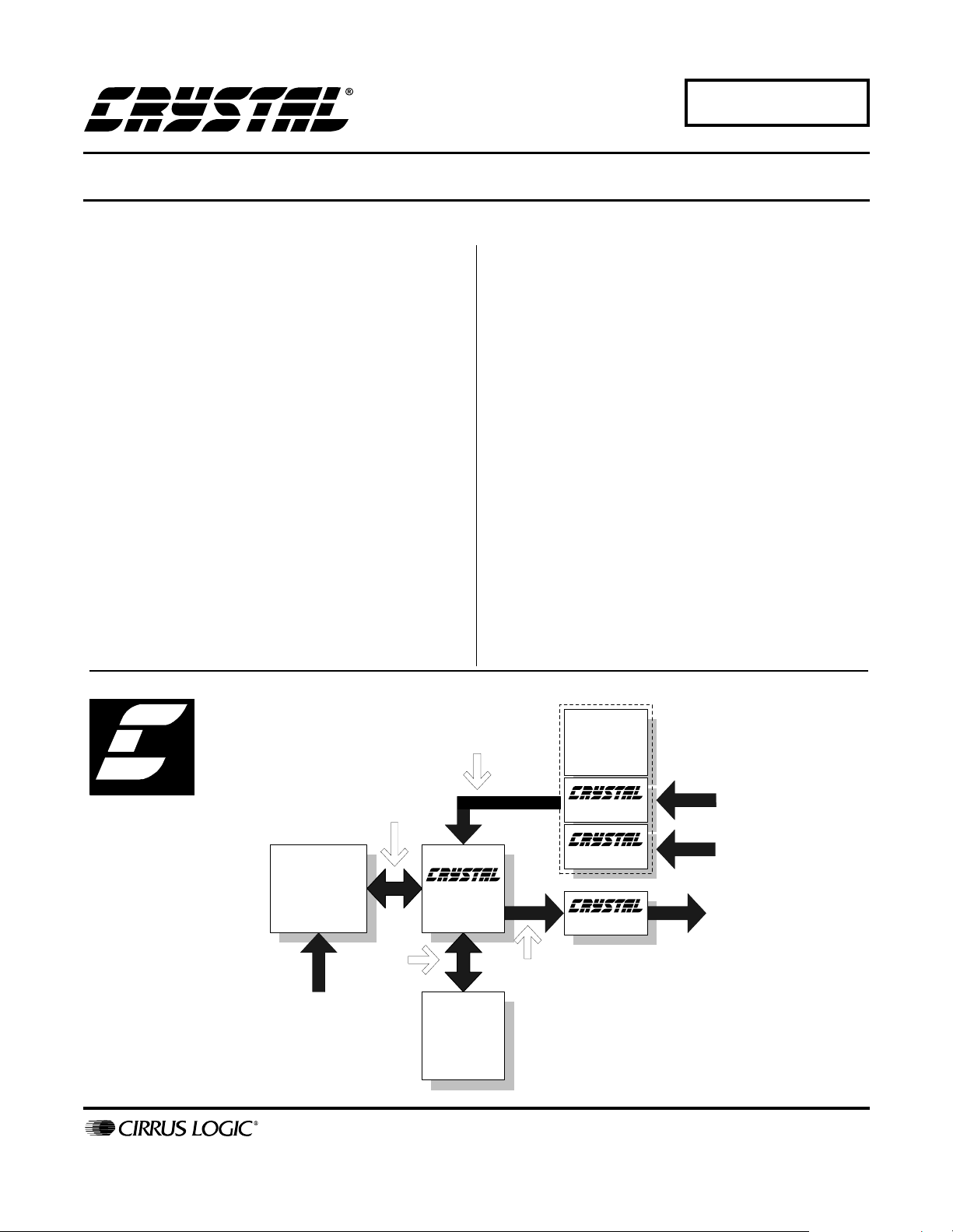
Input
CRYSTAL
PROCESSING
®
Host
µ
Controller
P.O. Box 17847, Austin, Texas 78760
(512) 445 7222 FAX: (512) 445 7581
http://www.cirrus.com
Host COMM
& Boot
EXT
Memory
Input
Configuration
MPEG
Transport
CS492x
Output
Configuration
64K x 8
ROM
Copyright Cirrus Logic, Inc. 1999
(All Rights Reserved)
DMX
DIR
ADC
DAC
S/PDIF
Analog Input
Multi-Channel
Analog Output
AUG ‘99
AN115REV2
1
Page 2

TABLE OF CONTENTS
1. OVERVIEW ............................................................................................................................... 5
1.1 Multi-Channel Decoder Family of Parts ................................. ...... ....... ...... .........................5
1.2 Document Strategy ............................................................................................................ 6
1.2.1 Hardware Documentation .....................................................................................6
1.2.2 CS4923/4/5/6/7/8/9 Application Code User’s Guides ........................................... 6
1.3 Using the CS4923/4/5/6/7/8/9 ............................................................................................7
2. HOST COMMUNICATION ........................................................................................................8
2.1 Serial Communication ........................................................................................................ 8
2.1.1 SPI Communication ..............................................................................................8
2.1.1.1 Writing in SPI ........................................................................................ 9
2.1.1.2 Reading in SPI ...................................................................................... 9
2
2.1.2 I
2.1.3 INTREQ Behavior: A Special Case .....................................................................14
2.2 Parallel Host Communication ........................................................................................... 17
2.2.1 Intel Parallel Host Communication Mode ............................................................18
2.2.2 Motorola Parallel Host Communication Mode .....................................................20
2.2.3 Procedures for Parallel Host Mode Communication ...........................................22
3. BOOT PROCEDURE & RESET ............................................................................................. 25
3.1 Host Boot ......................................................................................................................... 25
3.2 Autoboot ..........................................................................................................................28
3.2.1 Autoboot INTREQ Behavior ................................................................................ 31
3.3 Application Failure Boot Message ................................................................................... 32
3.4 Resetting the CS4923/4/5/6/7/8/9 ....................................................................................32
4. EXTERNAL MEMORY ..................... ...... ................................................................................ .34
4.1 Basic Memory Architecture ..............................................................................................35
4.2 Non-Paged Memory .........................................................................................................36
4.3 Paged Memory ................................................................................................................. 36
4.4 Examples ......................................................................................................................... 38
4.4.1 Non-Paged Memory ............................................................................................38
4.4.2 32 Kilobyte Paged Autoboot Memory .................................................................. 39
C Communication ............................................................................................. 12
2.1.2.1 W riting in I
2.1.2.2 Reading in I
2.2.1.1 Writing a Byte in Intel Mode ................................................................ 19
2.2.1.2 Reading a Byte in Intel Mode ..............................................................19
2.2.2.1 Writing a Byte in Motorola Mode .........................................................20
2.2.2.2 Reading a Byte in Motorola Mode .......................................................21
2.2.3.1 Control Write in a Parallel Host Mode .................................................22
2.2.3.2 Control Read in a Parallel Host Mode .................................................23
2
C ....................................................................................... 12
2
C .................................... ................................................. 13
Contacting Cirrus Logic Support
For a complete listing of Direct Sales, Distributor, and Sales Representative contacts, visit the Cirrus Logic web site at:
http://www.cirrus.com/corporate/contacts/
Preliminary product info rmation describes products which are i n production, but for whi ch ful l characterization data is not yet available. Advance produ ct i nfor mation describes products which are in development and subject to development changes. Cirrus Logic, Inc. has made best efforts to ensure that the information
contained in this document is accurate and reliable. However, the information is subject to change without notice and is provided “AS IS” without warranty of any
kind (express o r i mplie d). No re spon sibilit y is as sume d b y Cirru s Logic, Inc. for the use of this information, nor for infringements of patents or other rights of third
parties. This document is the property of Cirrus Logic, Inc. and implies no license under patents, copyrights, trademarks, or trade secrets. No part of this publication may be copied, reproduced, stored in a retrieval system, or transmitted, in any form or by any means (electronic, mechanical, photographic, or otherwise)
without the prior wri tten consent of Ci rrus Lo gic, Inc. Items fr om any Cir rus Logi c websit e or disk may be p rinte d for use by t he user . However , no part of the
printout or electronic files may be copied, reproduced, stored in a retrieval system, or transmitted, in any form or by any means (electronic, mechanical, photographic, or otherwise) wi thout the prior writ ten consent of Cirrus Log ic, I nc.F urt h erm ore, no part of this p ubl i c ati on may be used as a basis for manufacture or
sale of any items without the prior written consent of Cirrus Logic, Inc. The names of products of Cirrus Logic, Inc. or other vendors and suppliers appearing in
this document may be trademarks or service marks of their respect ive owner s which may be registered in some jurisdi ctions. A li st of Ci rru s Logic, Inc. trademarks and service marks can be found at http://www.cirrus.com.
2 AN115REV2
Page 3

4.4.3 64 Kilobyte Paged Autoboot Memory ................................................................. 40
4.4.4 64 Kilobyte Paged DTS & Autoboot Memory ...................................................... 41
4.5 CRD4923-MEM ............................................................................................................... 42
5. .HARDWARE CONFIGURATION .......................................................................................... 46
5.1 Address Checking ...........................................................................................................47
5.2 Input and Output .............................................................................................................. 47
5.2.1 Digital Audio Formats .......................................................................................... 47
5.2.2 Digital Input and Output Ports ............................................................................. 49
5.2.3 Parallel Delivery of Data ..................................................................................... 50
5.2.3.1 PCM Data Write in Parallel Host Mode ............................................... 50
5.2.3.2 Compressed Data Write in Parallel Host Mode .................................. 51
5.2.3.2.1 MFB Bit Example ....................................................................... 51
5.2.3.2.2 CMPREQ Example .................................................................... 52
5.3 Configuration Messages .................................................................................................. 52
5.3.1 Address Checking ............................................................................................... 52
5.3.2 Input ...................................................................................................................53
5.3.2.1 Special Considerations ....................................................................... 53
5.3.3 Output ................................................................................................................. 55
5.3.3.1 Special Considerations ....................................................................... 55
5.3.4 Creating Hardware Configuration Messages ...................................................... 56
6. APPENDIX A - PSEUDOCODE FOR THE CS4923/4/5/6/7/8/9 FAMILY .............................. 58
6.1 SPI Pseudocode .............................................................................................................. 58
6.1.1 SPI Write Operation ............................................................................................ 58
6.1.2 SPI Read Operation ............................................................................................ 59
2
6.2 I
C Pseudocode .............................................................................................................. 60
6.2.1 I
6.2.2 I
2
C Write Operation ............................................................................................. 60
2
C Read Operation ............................................................................................ 62
6.3 Typical Download Session with the CS4923/4/5/6/7/8/9 ................................................. 64
6.4 Typical Reset Sequence for the CS4923/4/5/6/7/8/9 ...................................................... 65
LIST OF FIGURES
Figure 1. SPI Write Flow Diagram................................................................................................... 9
Figure 2. SPI Read Flow Diagram ................................................................................................ 10
Figure 3. SPI Timing ..................................................................................................................... 11
Figure 4. I
Figure 5. I
Figure 6. I
Figure 7. Intel Mode, One-Byte Write Flow Diagram .................................................................... 19
Figure 8. Intel Mode, One-Byte Read Flow Diagram .................................................................... 20
Figure 9. Motorola Mode, One-Byte Write Flow Diagram............................................................. 21
Figure 10. Motorola Mode, One-Byte Read Flow Diagram........................................................... 21
Figure 11. Typical Parallel Host Mode Control Write Sequence Flow Diagram............................ 22
Figure 12. Typical Parallel Host Mode Control Read Sequence Flow Diagram............................ 23
Figure 13. Typical Serial Boot and Download Procedure ............................................................. 26
Figure 14. Typical Parallel Boot and Download Procedure........................................................... 27
Figure 15. Autoboot Memory Architecture .................................................................................... 28
Figure 16. Autoboot Timing Diagram............................................................................................ 29
Figure 17. Autoboot Sequence ..................................................................................................... 30
Figure 18. Autoboot INTREQ Behavior......................................................................................... 31
Figure 19. Performing a Reset...................................................................................................... 32
Figure 21. Autoboot Timing Diagram............................................................................................ 35
Figure 22. Run-Time Memory Access........................................................................................... 35
Figure 20. Basic Memory Architecture.......................................................................................... 35
2
C Write Flow Diagram................ ....... ...... ....... ...... ...... .............................................. ... 12
2
C Read Flow Diagram................................................................................................. 13
2
C Timing...................................................................................................................... 15
AN115REV2 3
Page 4

Figure 23. External Memory with 64 Kilobyte Pages.....................................................................37
Figure 24. External Memory With 32 Kbyte Pages ....................................................................... 37
Figure 25. Non-Paged Memory.....................................................................................................39
Figure 26. 32 Kbyte Paged memory..............................................................................................39
Figure 27. Autoboot Sequence for 32 Kbyte Paged Memory........................................................40
Figure 28. 64 Kbyte Paged Autoboot Memory ..............................................................................40
Figure 29. Autoboot for 64 Kbyte paged Memory .........................................................................41
Figure 30. 64 Kbyte Paged DTS/Autoboot Memory......................................................................42
Figure 31. Autoboot Sequence for DTS System using Symmetrical 64 Kilobyte Pages............... 43
Figure 32. CRD4923-MEM............................................................................................................45
Figure 33. Memory Map for CRD4923 Daughter Board................................................................46
Figure 34. DTS Autoboot Flow Diagrams...................................................................................... 46
Figure 35. I2S Format ................................................................................................................... 48
Figure 36. Left Justified Format.....................................................................................................48
Figure 37. Multi-Channel Format (M == 20)..................................................................................48
Figure 38. PCM Data Write Sequence in Parallel Host Mode Flow Diagram................................51
Figure 39. MFB Bit Status Polling Flow Diagram ..........................................................................52
Figure 40. CMPREQ Pin Status Polling Flow Diagram.................................................................52
LIST OF TABLES
Table 1. Serial Host Mode Configurations.......................................................................................8
Table 2. SPI Communication Signals..............................................................................................8
Table 3. I
Table 4. Parallel Host Mode Configurations..................................................................................17
Table 5. Intel Mode Communication Signals................................................................................. 18
Table 6. Motorola Mode Communication Signals..........................................................................20
Table 7. Boot Write Messages......................................................................................................25
Table 8. Boot Read Messages......................................................................................................25
Table 9. Memory Interface Pins .................................................................................................... 34
Table 10. Memory and Control Requirements for the CS4923/4/5/6/7/8/9 Family........................34
Table 11. ROM Speeds................................................................................................................. 36
Table 12. External Memory Configurations...................................................................................38
Table 13. DAI - Digital Audio Input Port ........................................................................................49
Table 14. CDI - Compressed Digital Input Port.............................................................................49
Table 15. DAO - Digital Audio Output Port.................................................................................... 49
Table 16. Output Channel Mapping .............................................................................................. 49
Table 17. Input Data Type Configuration ...................................................................................... 53
Table 18. Input Data Format Configuration...................... ...... ...... ....... ...... ....... ...... ....... ...... ....... ... 54
Table 19. Input SCLK Polarity Configuration................................................................................. 54
Table 20. FIFO Setup Configuration ............................................................................................. 54
Table 21. Output Clock Configuration ...........................................................................................55
Table 22. Output Data Format Configuration ................................................................................55
Table 23. Output MCLK Configuration..........................................................................................56
Table 24. Output SCLK Configuration........................................................................................... 56
Table 25. Output SCLK Polarity Configuration.............................................................................. 56
Table 26. Example Values to be Sent to CS492X After Download or Soft Reset.........................57
2
C Communication Signals .... ...... ....... .......................................................................... 1 2
4 AN115REV2
Page 5

1. OVERVIEW
The CS4923/4/5/6/7/8/9 is a family of system on a
chip solutions for multi-channel audio
decompression and digital signal processing. Since
the part is RAM-based, a download of application
software is required each time the
CS4923/4/5/6/7/8/9 is powered up.
Digital bitstream); used primarily in broadcast environments.
PES - a Packetized Elementary Stream (PES) bitstream contains the elementary compressed audio
stream and additional header information which
can be used for A/V synchronization; used primarily in broadcast environments.
These parts are generally ta rgeted at two differ ent
market segments. The broadcast market where
audio/video (A/V) synchronization is required, and
the outboard decoder markets where audio/video
synchronization is not required. The important
differentiation is the format in which the data will
be received by the CS4923/4/5/6/7/8/9. In systems
where A/V synchronization is required from the
CS4923/4/5/6/7/8/9, the incoming data is typically
PES encoded. In an outboard decoder application
the data typically comes in the IEC61937 format
(as specified by the DVD consortium). An
important point to remember is that the
CS4923/4/5/6/7/8/9 will support both
environments, but different downloads are required
depending on the input data type.
Broadcast applications include (but are not limited
to) set top box applications, DVDs and digital TVs.
Outboard decoder applications include standalone
decoders and audio/video receivers. Often times a
system may be a hybrid between an outboard
decoder and a broadcast system depending on its
functionality.
As discussed above, compressed audio can be
packed in IEC61937, PES, or elementary formats
depending on the decoder environment. Each format is supported by a separate download of application code. Consult the relevant Application Code
User’s Guide to determine which format s are supported by a particular application. A brief description of each format is presented below.
Elementary - an elementary bitstream consists only
of compressed audio data (e.g., strictly the Dolby
IEC61937 - a method of packing compressed audio
such that it can be delivered using a bi-phase encoded signal (e.g., S/PDIF output signal from DVD
player); used primarily for outboard decoders
where A/V synchronization is not required.
1.1 Multi-Channel Decoder Family of Parts
CS4923 - Dolby Digital
CS4923 is the original member of the family and is
intended to be used if only Dolby Digital decoding
is required. For Dolby Digital, post processing
includes bass management, delays and Dolby Pro
Logic decoding. Separate downloads can also be
used to support stereo to 5.1 channel effects
processing and stereo MPEG decoding.
CS4924 - Dolby Digital
Decoder. The CS4924 is the stereo version of the
CS4923 designed for source products such as
DVD, HDTV, and set-top boxes. Separate
downloads are available for stereo decode of Dolby
Digital and MPEG audio.
CS4925 - International Multi-Channel DVD
Audio Decoder. The CS4925 supports both Dolby
Digital and MPEG-2 multi-channel formats. For
both Dolby Digital and MPEG-2 multi-channel,
post processing includes bass management and
Dolby Pro Logic decoding. Separate downloads are
available for decode of Dolby Digital and MPEG
audio. Another code load can be used to support
stereo to 5.1 channel effects processing.
CS4926 - DTS/Dolby® Multi-Channel Audio
Decoder. The CS4926 supports both Dolby Digital
and DTS, or Digital Theater Surround. For Dolby
Digital, post processing includes bass management
TM
Audio Decoder. The
TM
Source Product
AN115REV2 5
Page 6

and Dolby Pro Logic. The Dolby Digital code and
DTS code take separate code downloads. Separate
downloads can also be used to support stereo to 5.1
channel effects processing and stereo MPEG
decoding.
CS4927 - MPEG-2 Multi-Channel Decoder. The
CS4927 supports MPEG-2 multi-channel decoding
and should be used in applications where Dolby
Digital decoding is not necessary. For MPEG-2
multi-channel decoding, post processing includes
bass management and Dolby Pro Logic decoding.
Another code load can be used to support stereo to
5.1 channel effects processing.
CS4928 - DTS Multi-Channel Decoder. The
CS4928 supports DTS multi-channel decoding and
should be used in applications where Dolby Digital
decoding is not necessary. For DTS multi-channel
decoding, post processing includes bass
management. Separate downloads can also be used
to support stereo to 5.1 channel effects processing
and stereo MPEG decoding.
CS4929 - AAC 2-Channel, (Low Complexity) and
MPEG-2 Stereo Decoder. The CS4929 is capable
of decoding both 2-channel AAC and MPEG-2
audio. The CS4929 supports elementary and PES
formats.
1.2 Document Strategy
Multiple documents are needed to fully define,
understand and implement the functionality of the
CS4923/4/5/6/7/8/9. They can be split up into two
basic groups: hardware and application code
documentation. It should be noted that hardware
and application code are co-dependent and one can
not successfully use the part without an
understanding of both. The ‘ANXXX’ notation
denotes the application note number under which
the respective user’s guide was released.
1.2.1 Hardware Documentation
CS4923/4/5/6/7/8/9 Family Data Sheet - This
document describes the el ec tric al char acte ristic s of
the device from timing to base functionality. This is
the hardware designers tool to learn the part’s
electrical and systems requirements.
AN115 - CS4923/4/5/6/7/8/9 Hardware User’s
Guide - describes the functional aspects of the
device. An in depth description of communication,
boot procedure, external memory and hardware
configuration are given in this document. This
document will be valuable to both the hardware
designer and the system programmer.
1.2.2 CS4923/4/5/6/7/8/9 Application Code
User’s Guides
The following application notes describe the
application codes used with the
CS4923/4/5/6/7/8/9. Whenever an application code
user’s guide is referred to, it should be assumed that
one or more of the below documents are being
referenced. The following list covers currently
released application notes. This list will grow with
each new application released. For a current list of
released user’s guides please see www.crystal.com
and search for the part number.
AN120 - Dolby Digital User’s Guide for the
CS4923/4/5/6. This document covers the features
available in the Dolby Digital code including
delays, pink noise, bass management, Pro Logic,
PCM pass through and Dolby Digital processing
features. Optional appendices are available that
document code for Dolby Virtual, Q-Surround and
VMAx.
AN121 - MPEG User’s Guide for the CS4925.
This document covers the features available in the
MPEG Multi-Channel code including delays, bass
management, Pro Logic, and MPEG processing
features.
AN122 - DTS User’s Guide for the CS4926,
CS4928. This document covers the features
available in the DTS code including bass
management and DTS processing features.
6 AN115REV2
Page 7

AN123 - Surround User’s Guide for the
CS4923/4/5/6/7/8. This code covers the different
Stereo PCM to surround effects processing code.
Optional appendices are available that document
Crystal Original Surround, Circle Surround and
Logic 7.
AN140 - Broadcast Systems Guide for the
CS4923/4/5/6/7/8/9. This guide describes all
application code (e.g. Dolby Digital, MPEG, AAC)
designed for broadcast systems such as HDTV and
set-top box receivers. This document also provides
a discussion of broadcast system considerations
and dependencies such as A/V synchronization and
channel change procedures.
1.3 Using the CS4923/4/5/6/7/8/9
No matter what application is being used on the
chip, the following four steps are always followed
to use the CS4923/4/5/6/7/8/9 in system.
1) Reset and/or Download Code - Detailed
information in AN115
2) Hardware Configuration - Detailed information
in AN115
3) Application configuration - Detailed
information in the appropriate Application
Code User’s guide
4) Kickstart - This is the “Go” command to the
CS492X once the system is properly
configured. Information can be found in the
appropriate Application Code User’s guide.
For this document, CS4923/4/5/6/7/8/9 has been
replaced in certain places with CS492X for
readability. Unless otherwise specified CS492X
should be interpreted as applying to the CS4923,
CS4924, CS4925 and CS4926.
AN115REV2 7
Page 8
2. HOST COMMUNICATION
The host communication port of the
CS4923/4/5/6/7/8/9 is used for downloading
application code to the DSP and it is used for
communicating with the DSP during run-time. The
CS492X supports two parallel host communication
modes (Intel mode and Motorola mode) and two
serial host communication modes (I2C and SPI).
Please note that when a parallel host
communication mode has been selected, the
external memory interface cannot be used. This
constraint has two significant implications:
• Autoboot cannot be used in a system using
parallel host communication
• Parallel host communication modes cannot be
used when processing DTS (CS4926 or CS4928)
Each of the host communication modes supported
by the CS492X family will be discussed in
subsequent sections. The following information
will be provided for each mode:
• How to configure the CS492X for each host
communication mode
• Which pins of the CS492X must be used
• The protocol used for writing to the CS492X
• The protocol used for reading from the CS492X
2.1 Serial Communication
The CS4923/4/5/6/7/8/9 has a serial control port
that supports both SPI and I2C forms of
communication. The mode of communication is
determined by the states of the RD (pin 5) and WR
(pin 4) pins at the rising edge of RESET (pin 36).
Table 1 below shows the two possible mode
configurations:
Other modes are not supported at this time and
should not be used. If the mode pins are driven
dynamically by the host, then set up (t
) and hold
rstsu
RD WR MODE
01
10 SPI
Table 1. Serial Host Mode Configurations
(t
) times must be satisfied around the rising
rsthld
2
C
I
edge of reset as specified in the RESET Switching
characteristics portion of the CS492X Family
Datasheet.
The following sections will explain each
communication mode in more detail. Flow
diagrams will illustrate read and write cycles.
Pseudocode is presented in “Appendix A Pseudocode For The CS4923/4/5/6/7/8/9 Family”
58 to demonstrate communication with the chip
from a programming perspective.
Timing diagrams will be shown to demonstrate
relative edge positions of signal transitions for read
and write operations.
Only the subsection describing the communication
mode being used needs to be read by the system
designer.
2.1.1 SPI Communication
SPI communication with the CS4923/4/5/6/ 7/8/9 is
accomplished with 5 communication lines: chip
select, serial control clock, serial data in, serial data
out and an interrupt request line to signal that the
DSP has data to transmit to the host. Table 2 shows
the mnemonic, pin name and pin number of each of
these signals on the CS4923/4/5/6/7/8/9.
Mnemonic Pin Name Pin Number
Chip Select CS
Serial Clock SCCLK 7
Serial Data In SCDIN 6
Serial Data Out SCDOUT 19
Interrupt Request INTREQ
Table 2. SPI Communication Signals
18
20
8 AN115REV2
Page 9
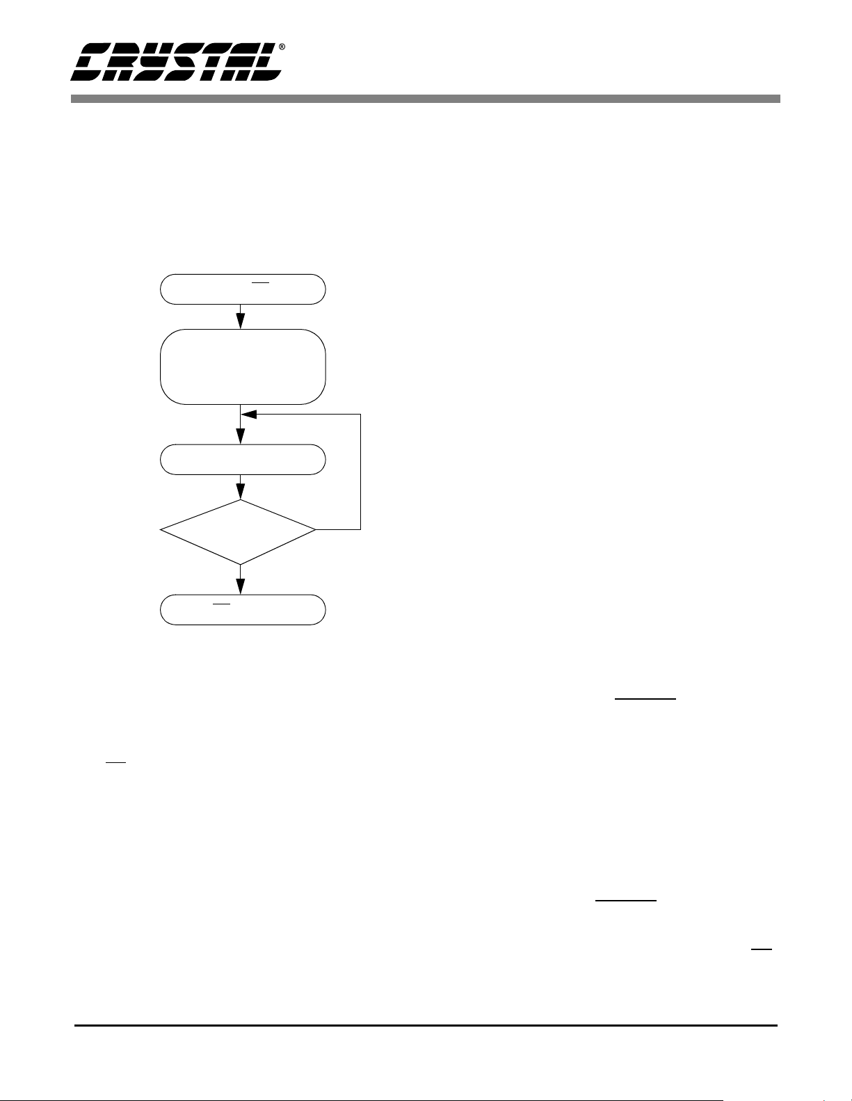
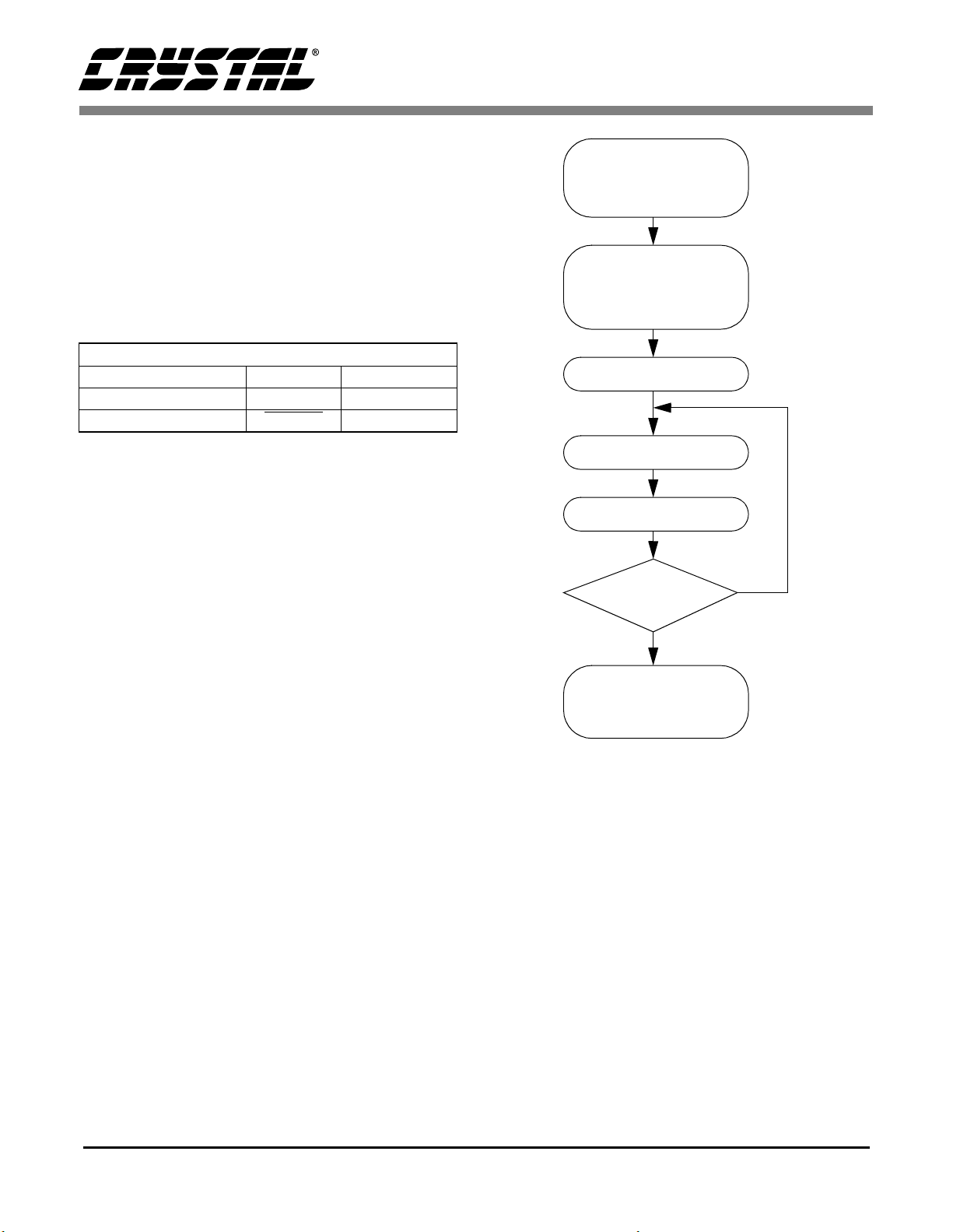
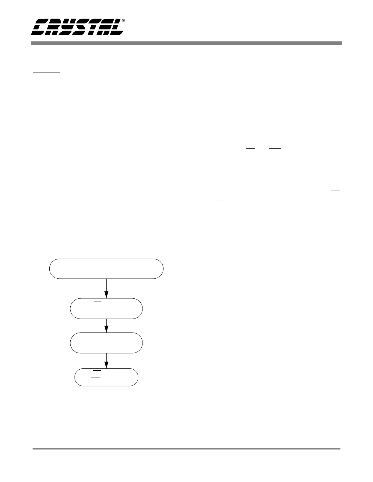
2.1.1.1 Writing in SPI
Figure 1. SPI Write Flow Diagram
SPI START: CS (LOW)
WRITE ADDRESS BYTE
SET TO 0 FOR WRITE
SEND DATABYTE
MORE DATA?
CS
(HIGH)
WITH MODE BIT
N
Y
When writing to the device in SPI the same
protocol will be used whether writing a byte, a
message or even an entire executable download
image. The examples shown in this document can
be expanded to fit any write situation. Figure 1
shows a typical write sequence:
3) The host should then clock data into the device
most significant bit first, one byte at a time. The
data byte is transferred to the DSP on the falling
edge of the eighth serial clock. For this reason,
the serial clock should be default low so that
eight transitions from low to high to low will
occur for each byte.
4) When all of the bytes have been transferred,
chip select should be raised to signify an end of
write. Once again it is crucial that the serial
clock transitions from high to low on the last bit
of the last byte before chip select is raised, or a
loss of data will occur.
The pseudocode in Section 6.1.1 “SPI Write
Operation” -- page 58 demonstrates a write
operation for the SPI mode of communication.
The same write routine could be used to send a
single byte, message or an entire application code
image. From a hardware perspective, it makes no
difference whether communication is by byte or
multiple bytes of any length as long as the correct
hardware protocol is followed.
The following is a detailed description of an SPI
write sequence with the CS492X.
1) An SPI transfer is initiated when chip select
(CS) is driven low.
2) This is followed by a 7-bit address and the
read/write bit set low for a write. The address
for the CS492X defaults to 0000000b. It is
necessa ry to clo ck this address in prior to any
transfer in order for the CS492X to accept the
write. In other words a byte of 0x00 should be
clocked into the device preceding any write. The
0x00 byte represents the 7 bit address 0000000b,
and the least significant bit set to 0 to designate
a write.
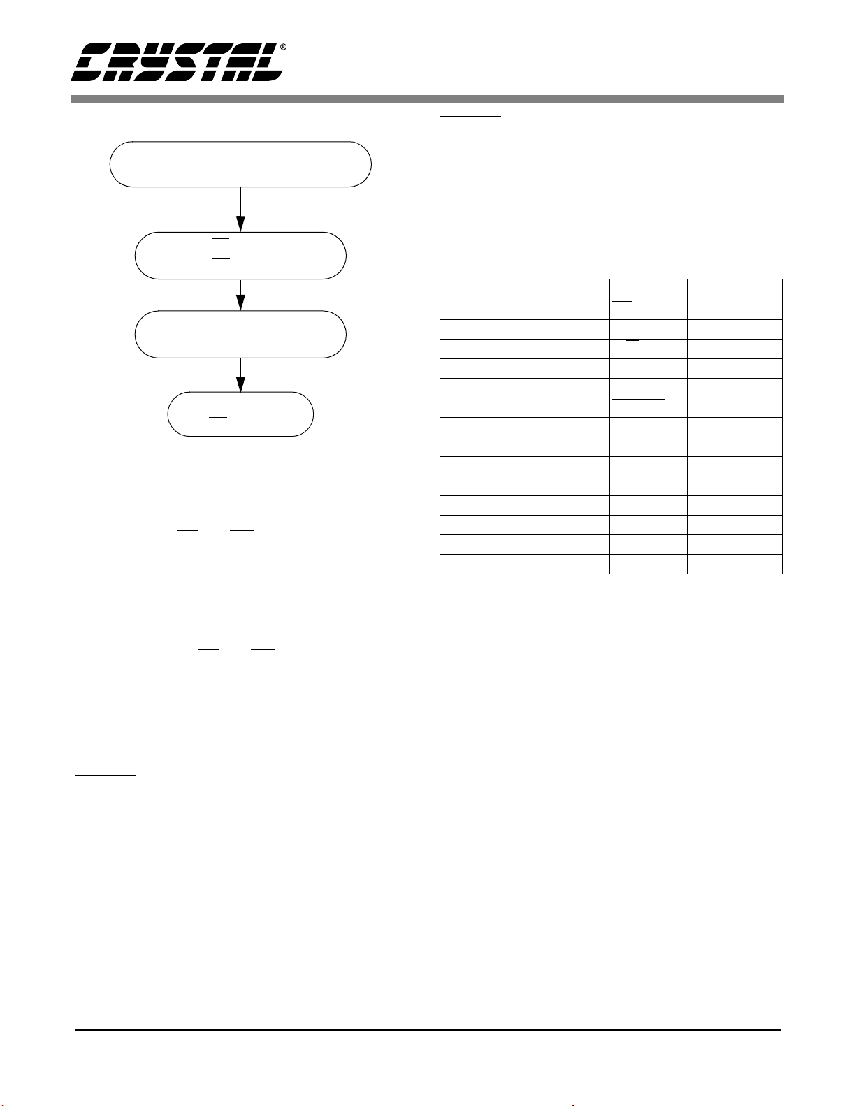
2.1.1.2 Reading in SPI
A read operation is necessary when the
CS4923/4/5/6/7/8/9 signals that it has data to be
read. The CS492X does this by dropping its
interrupt request line (INTREQ) low. When
reading from the device in SPI, the same protocol
will be used whether reading a single byte or
multiple bytes. The examples shown in this
document can be expanded to fit any read situation.
Figure 2 shows a typical read sequence:
The following is a detailed description of an SPI
read sequence with the CS492X.
1) An SPI read transaction is initiated by the
CS492X dropping INTREQ, signaling that it
has data to be read.
2) The host responds by driving chip select (CS)
low.
AN115REV2 9
Page 10
Figure 2. SPI Read Flow Diagram
CS (LOW)
WRITE ADDRESS BYTE
SET TO 1 FOR READ
READ DATA BYTE
INTREQ STILL LOW?
CS (HIGH)
WITH MODE BIT
NO
YES
INTREQ LOW?
YES
NO
3) This is followed by a 7-bit address and the
read/write bit set high for a read. The address
for the CS492X defaults to 0000000b. It is
necessary to clock this address in prior to any
transfer in order for the CS492X to
acknowledge the read. In other words a byte of
0x01 should be clocked into the device
preceding any read. The 0x01 byte represents
the 7 bit address 0000000b, and the least
significant bit set to 1 to designate a read.
4) After the falling edge of the serial control clock
(SCCLK) for the read/write bit, the data is
ready to be clocked out on the control data out
pin (CDOUT). Data clocked out by the host is
valid on the rising edge of SCCLK and data
transitions occur on the falling edge of S CCLK.
The serial clock should be default low so that
eight transitions from low to high to low will
occur for each byte.
5) If INTREQ is still low, another byte should be
clocked out of the CS492X. Please see the
discussion below for a complete description of
INTREQ behavior.
6) When INTREQ has risen, the chip select line of
the CS492X should be raised to end the read
transaction.
Understanding the role of INTREQ is important for
successful communication. INTREQ is guaranteed
to remain low (once it has gone low) until the
second to last rising edge of SCCLK of the last byte
to be transferred out of the CS492X. If there is no
more data to be transferred, INTREQ will go high
at this point. For SPI this is the rising edge for the
second to last bit of the last byte to be transferred.
After going high, INTREQ is guaranteed to stay
high until the next rising edge o f SCC LK. This end
of transfer condition signals the host to end the read
transaction by clocking the last data bit out and
raising CS. If INTREQ is still low after the second
to last rising edge of SCCLK, the host should
continue reading data from the serial control port.
It should be noted that all data should be read out of
the serial control port during one cycle or a loss of
data will occur. In other words, all data should be
read out of the chip until INTREQ signals the last
byte by going high as described above. Please see
Section 2.1.3 “INTREQ Behavior: A Special Case”
-- page 10 for a more detailed description of
INTREQ behavior.
The pseudocode in Section 6.1.2 “SPI Read
Operation” -- page 59 demonstrates a read
operation for the SPI mode of communication.
The Figure 3 timing diagram shows the relative
edges of the control lines for an SPI read and write.
10 AN115REV2
Page 11
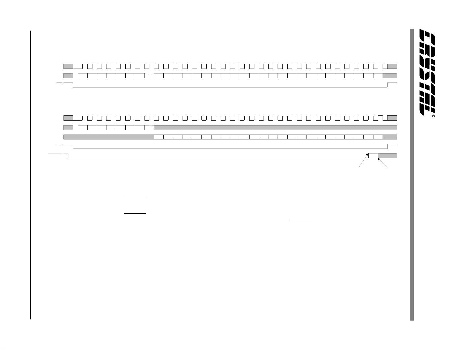
AN115REV2 11
SCCLK
SCDIN
CS
SCCLK
SCDIN
SCDOUT
CS
INTREQ
AD6 AD4AD5 AD3 AD2 AD1 AD0 R/W D7 D6 D5 D4 D3 D2 D1 D0 D7 D6 D5 D4 D 3 D2 D1 D0 D7 D6 D5 D4 D3 D2 D1 D0
SPI Write Functional Timing
AD6 AD4AD5 AD3 AD2 AD1
AD0
R/W
D7 D6 D5 D4 D3 D2 D1 D0 D7 D6 D5 D4 D3 D2 D1 D0 D7 D6 D5 D4 D3 D2 D1 D0
Notes: 1. INTRE Q
to be transferred out of the CS4923/4/5/6/7/8/9.
2. INTREQ
may go LOW again if there is new data to be read. The condition of INTREQ
point should be treated as a new read condition. After a stop condition, a new start condition
and an address byte should be sent
SP I R ead F unc tional Tim ing
Note1
is guaranteed to stay LOW until the rising edge of SCCLK for bit D1 of the last byte
is guaranteed to remain HIGH until the next rising edge of SCCLK at which point it
going LOW at this
Figure 3. SPI Timing
Note 2
Page 12
2.1.2 I2C Communication
I2C communication with the CS4923/4/5/6/7/8/9 is
accomplished with 3 communication lines: serial
control clock, a bi-directional serial data
input/output line and an interrupt request line to
signal that the DSP has data to t ransmi t to the host.
Table 3 shows the mnemonic, pin name and pin
number of each of these signals on the CS492X.
Mnemonic Pin Name Pin Number
Serial Clock SCCLK 7
Bi-Directional Data SCDIO 19
Interrupt Request INTREQ
Table 3. I
2
C Communication Signals
Typically in I2C communication SCDIO is an open
drain line with a pull-up. A logic one is placed on
the line by tri-stating the output and allowing the
pull-up to raise the line. At this point another
device can drive the line low if necessary. Tristating SCDIO can have two effects: 1. To send out
a one when writing data or sending a “no
acknowledge”; 2. release the line when another
chip is writing data.
For our pseudocode examples, driving SCDIO high
effectively tri-states this signal since it is open
drain and SCDIO (HIGH) should be interpreted as
such.
20
SEND I2C START:
DROP SCDIO LOW
WHILE SCCLK IS HIGH
WRITE ADDRESS BYTE
WITH MODE BIT
SET TO 0 FOR WRITE
GET ACK
SEND DATABYTE
GET ACK
MORE DATA?
N
2
C STOP:
I
RAISE SCDIO HIGH
WHILE SCCLK IS HIGH
Figure 4. I2C Write Flow Diagram
Y
2.1.2.1 Writing in I2C
2) Next a 7-bit address with the read/write bit set
When writing to the device in I2C the same
protocol will be used whether writing a byte, a
message or even an application code image. The
examples shown in this document can be expanded
to fit any write situation. Figure 4 shows a typical
write sequence:
The following is a detailed description of an I2C
write sequence with the CS492X.
1) An I2C transfer is initiated with an I2C start
condition which is defined as the data (SCDIO)
line falling while the clock (SCCLK) is held
high.
12 AN115REV2
low for a write should be sent to the CS492X.
The address for the CS492X defaults to
0000000b. It is necessary to clock this address
in prior to any transfer in order for the CS492X
to accept the write. In other words a byte of
0x00 should be clocked into the device
preceding any write. The 0x00 byte represents
the 7 bit of address (0000000b) and the
read/write bit set to 0 to designate a write.
Page 13
3) After each byte (including the address and each
data byte) the host must release the data line
and provide a ninth clock for the CS492X to
acknowledge. The CS492X will drive the data
line low during the ninth clock to acknowledge.
If for some reason the CS492X does not
acknowledge, it means that the last byte sent
was not received and should be resent. If the
resent byte fails to produce an acknowledge, a
stop condition should be sent and the device
should be reset.
4) The host should then clock data into the device
most significant bit first, one byte at a time. The
CS492X will (and must) acknowledge each
byte that it receives which means that after each
byte the host must provide an acknowledge
clock pulse on SCCLK and release the data
line, SCDIO.
5) At the end of a data transfer a stop condition
must be sent. The stop condition is defined as
the rising edge of SCDIO while SCCLK is
high.
INTREQ LOW?
NO
YES
SEND I2C START:
DROP SCDIO LOW
WHILE SCCLK IS HIGH
WRITE ADDRESS BYTE
WITH MODE BIT
SET TO 1 FOR READ
GET ACK
READ DATABYTE
The pseudocode in Section 6.2.1 “I2C Write
Operation” -- page 60 demonstrates a write
operation for the I2C mode of communication.
2.1.2.2 Reading in I2C
A read operation is necessary when the
CS4923/4/5/6/7/8/9 signals that it has data to be
read. It does this by dropping its interrupt request
line (INTREQ) low. When reading from the device
in I2C, the same protocol will be used whether
reading a single byte or multiple bytes. The
examples shown in this document can be expanded
to fit any read situation. Figure 5 shows a typical
I2C read sequence
1) An I2C read transaction is initiated by the
CS492X dropping INTREQ, signaling that it
has data to be read.
YES
INTREQ STILL LOW?
NO
SEND NACK
SEND I2C STOP:
RISING EDGE OF SCDIO
WHILE SCLK IS HIGH
Figure 5. I2C Read Flow Diagram
SEND ACK
2) The host responds by sending an I2C start
condition which is SCDIO dropping while
SCCLK is held high.
AN115REV2 13
Page 14

3) The start condition is followed by a 7-bit
address and the read/write bit set high for a
read. The address for the CS492X defaults to
0000000b. It is necessary to clock this address
in prior to any transfer in order for the CS492X
to acknowledge the read. In other words a byte
of 0x01 should be clocked into the device
preceding any read. The 0x01 byte represents
the 7 bit address 0000000b and a read/write bit
set to 1 to designate a read.
4) After the falling edge of the serial control clock
(SCCLK) for the read/write bit of the address
byte, an acknowledge must be read in by the
host. The CS492X will drive SCDIO low to
acknowledge the address byte and to indicate
that it is ready for a read operation. If an
acknowledge is not sent by the CS492X, a stop
condition should be issued and the read
sequence should be restarted.
5) The data is ready to be clocked out on the
SCDIO line at this point. Data clocked out by
the host is valid on the rising edge of SCCLK
and data transitions occur on the falling edg e of
SCCLK.
6) If INTREQ is still low after a byte transfer, an
acknowledge (SCDIO clocked low by SCCLK)
must be sent by the host to the CS492X and
another byte should be clocked out of the
CS492X. Please see the discussion below for a
complete description of INTREQ’s behavior.
7) When INTREQ has risen, a no acknowledge
should be sent by the host (SCDIO clocked
high by the host) to the CS492X. This, followed
by an I2C stop condition (SCDIO raised, while
SCCLK is high) signals an end of read to the
CS492X.
Understanding the role of INTREQ is important for
successful communication. INTREQ is guaranteed
to remain low (once it has gone low), until the
rising edge of SCCLK for the last bit of the last byte
to be transferred out of the CS492X (i.e . the rising
edge of SCCLK before the ACK SCCLK). If there
is no more data to be transferred, INTREQ will go
high at this point. After going high, INTREQ is
guaranteed to stay high until the next rising edge of
SCCLK (i.e. it will stay high until the rising edge
of SCCLK for the ACK/NACK bit). This end of
transfer condition signals the host to end the read
transaction by clocking the last data bit out of the
CS492X and then sending a no acknowledge to the
CS492X to signal that the read sequence is over. At
this point the host should send an I2C stop
condition to complete the read sequence. If
INTREQ is still low after the rising edge of
SCCLK on the last data bit of the current byte, the
host should send an acknowledge and continue
reading data from the serial control port.
It should be noted that all data should be read out of
the serial control port during one cycle or a loss of
data will occur. In other words, all data should be
read out of the chip until INTREQ signals the last
byte by going high as described above. Please see
Section 2.1.3 “INTREQ Behavior: A Special Case”
-- page 10 for a more detailed description of
INTREQ behavior.
The pseudocode in Section 6.2.2 “I2C Read
Operation” -- page 62 demonstrates a read
operation for the I2C mode of communication.
The timing diagram in Figure 6 shows the relative
edges of the control lines for an I2C read and write.
2.1.3 INTREQ Behavior: A Special Case
When communicating with the CS4923/4/5/6/7/8/9
there are two types of messages which force
INTREQ to go low. These messages are known as
solicited messages and unsolicited messages. For
more information on the specific types of messages
that require a read from the host, one of the
application code user’s guides should be
referenced.
In general, when communicating with the CS492X,
INTREQ will not go low unless the host first sends
14 AN115REV2
Page 15
AN115REV2 15
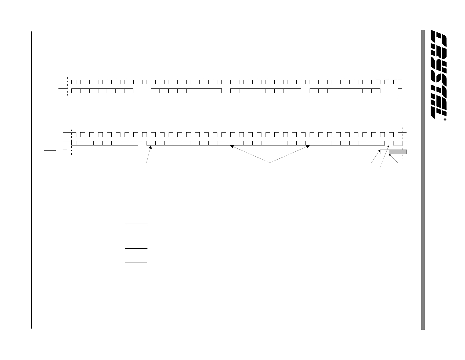
I2CStart I2CStop
SCCLK
SCDIO
AD6 AD4AD5 AD3 AD2 AD1 AD0 R/W D7 D6 D5 D4 D3 D2 D1 ACKD0ACK D7 D6 D5 D4 D3 D2 D1 ACKD0 D7 D6 D5 D4 D3 D2 D1 ACKD0
I2C Write Functional Timing
I2CStart I2CStop
SCCLK
SCDIO
INTREQ
AD6 AD4AD5 AD3 AD2 AD1 AD0 R/W D7 D6 D5 D4 D3 D2 D1 ACKD0ACK D7 D6 D5 D4 D3 D2 D1 ACKD0 D 7 D6 D5 D4 D3 D2 D1 NACKD0
Note 1 Note 3
Note 2
I2CReadFunctionalTiming
Notes: 1. The ACK for the address byte is driven by the CS4923/4/5/6/7/8/9.
2. The ACKs for the data bytes being read from the CS4923/4/5/6/7/8/9 should be driven by the
host.
3. INTREQ
is guaranteed to stay LOW until the rising edge of SCCLK for bit D0 of the last byte
to be transferred out of the CS4923/4/5/6/7/8/9.
4. A NACK should be sent by the host after the last byte to indicate the end of the read cycle.
5. INTREQ
is guaranteed to stay HIGH until the next rising edge of SCCLK (for the ACK/NACK
bit) at which point it may go LOW again if there is new data to be read. The condition of
INTREQ
going LOW at this point should be treated as a new read condition. After a stop
condition, a new start condition followed by an address byte should be sent.
Figure 6. I2C Timing
Note 4
Note 5
Page 16

a read request command message. In other words
the host must solicit a response from the DSP. In
this environment, the host must read from the
CS492X until INTREQ goes high again. Once the
INTREQ pin has gone high it will not be driven low
until the host sends another read request.
When unsolicited messages, such as those used for
Autodetect, have been enabled, the behavior of
INTREQ is noticeably different. The CS492X will
drop the INTREQ pin whenever the DSP has an
outgoing message, even though the host may not
have requested data.
There are three ways in which INTREQ can be
affected by an unsolicited message:
1) During normal operation, while INTREQ is
high, the DSP could drop INTREQ to indicate an
outgoing message, without a prior read request.
2) The host is in the process of reading from the
CS492X, meaning that INTREQ is already low. An
unsolicited message arrives which forces INTREQ
to remain low after the solicited message is read.
3) The host is reading from the CS492X when the
unsolicited message is queued, but INTREQ goes
high for one period of SCCLK and then goes low
again before the end of the read cycle.
In case (1) the host should perform a read operation
as discussed in the previous sections.
In case (2) an unsolicited message arrives before
the second to last SCCLK of the final byte transfer
of a read, forcing the INTREQ pin to remain low.
In this scenario the host should continue to read
from the CS492X without a stop/start condition or
data will be lost.
In case (3) an unsolicited message arrives between
the second to last SCCLK and the last SCCLK of
the final byte transfer of a read. In this scenario,
INTREQ will transition high for one clock (as if the
read transaction has ended), and then back low
(indicating that more data has queued). This final
case is the most com plicated and shall be expl ained
in detail.
There are two constraints which completely
characterize the behavior of the INTREQ pin
during a read. The first constraint is that the
INTREQ pin is guaranteed to remain low until the
second to last SCCLK (SCCLK number N-1) of the
final byte being transferred from the CS492X (not
necessarily the second to last bit of the data byte).
The second constraint is that once the INTREQ pin
has gone high it is guaranteed to remain high until
the rising edge of the last SCCLK (SCCLK number
N) of the final byte being transferred from the
CS492X (not necessarily the last bit of the data
byte). If an unsolicited message arrives in the
window of time between the rising edge of the
second to last SCCLK and the final SCCLK,
INTREQ will drop low on the rising edge of the
final SCCLK as illustrated in the functional timing
diagrams shown for I2C and SPI read cycles.
INTREQ behavior for I2C communication is
illustrated in figure 6. When using I2C
communication the INTREQ pin will remain low
until the rising edge of SCCLK for the data bit D0
(SCCLK N-1), but it can go low at the rising edge
of SCCLK for the NACK bit (SCCLK N) if an
unsolicited message has arrived. If no unsolicited
messages arrive, the INTREQ pin will remain high
after rising.
INTREQ behavior for SPI communication is
illustrated in figure 3. When using SPI
communication, the INTREQ pin will remain low
until the rising edge of SCCLK for the data bit D1
(SCCLK N-1), but it can go low at the rising edge
of SCCLK for data bit D0 (SCCLK N) if an
unsolicited message has arrived. If no unsolicited
messages arrive, the INTREQ pin will remain high
after rising.
Ideally, the host will sample INTREQ on the
falling edge of SCCLK number N-1 of the final
byte of each read response message. If INTREQ is
16 AN115REV2
Page 17

sampled high, the host should conclude the current
read cycle using the stop condition defined for the
communication mode chosen. The host should then
begin a new read cycle complete with the
appropriate start condition and the chip address. If
INTREQ is sampled low, the host should continue
reading the next message from the CS492X
without ending the current read cycle.
When using automated communication ports,
however, the host is often limited to sampling the
status of INTREQ after an entire byte has been
transferred. In this situation a low-high-low
transition (case 3) would be missed and the host
will see a constantly low INTREQ pin. Since the
host should read from the CS492X until it detects
that INTREQ has gone high, this condition will be
treated as a multiple-message read (more than one
read response is provided by the CS492X). Under
these conditions a single byte of 0x00 will be read
out before the unsolicited message.
The length of every read response is defined in the
user’s manual for each piece of application code.
Thus, the host should know how many bytes to expect
based on the first byte (the OPCODE) of a read
response message. It is guaranteed that no read
responses will begin with 0x00, which means that a
NULL byte (0x00) detected in the OPCODE position
of a read response message should be discarded.
Please see an Application Code User’s Guide for an
explanation of the OPCODE.
It is important that the host be aware of the
presence of NULL bytes, or the communication
channel could become corrupted.
When case (3) occurs and the host issues a stop
condition before starting a new read cycle, the first
byte of the unsolicited message is loaded directly
into the shift register and 0x00 is never seen.
Alternatively, if case (3) occurs and the host continues to read from the CS492X without a stop condition (a multiple message read), the 0x00 byte
must be shifted out of the CS492X before the first
byte of the unsolicited message can be read.
In other words, if a system can only sample
INTREQ after an entire byte transfer the following
routine should be used if INTREQ is low after the
last byte of the message being read:
1) Read one byte
2) If the byte == 0x00 discard it and skip to step 3.
If the byte != 0x00 then it is the OPCODE for
the next message. For this case skip to step 4.
3) Read one more byte. This is the OPCODE for
the next message.
4) Read the rest of the messag e as indicat ed in the
previous sections.
2.2 Parallel Host Communication
The parallel host communication modes of the
CS4923/4/5/6/7/8/9 provide an 8-bit interface to
the DSP. An Intel-style parallel mode and a
Motorola-style parallel mode are supported. The
mode of communication is determined by the states
of the RD (pin 5), WR (pin 4), and PSEL (pin 19)
pins at the rising edge of RESET (pin 36). Each
time the CS492X is reset, the RD, WR, and PSEL
pins are sampled to determine how the host
interface port will be configured. Table 4 shows the
necessary pin configurations for selecting a parallel
configuration mode.
RD WR PSEL MODE
1 1 0 Intel Mode
1 1 1 Motorola Mode
Table 4. Parallel Host Mode Configurations
The host interface is implemented using four
communication registers within the CS492X:
• The Host Message register (A[1:0]==00b):
receives incoming control data bytes and
provides outgoing response data bytes.
AN115REV2 17
Page 18
• The Host Control register (A[1:0]=01b):
provides information about the state of the
communication interface.
• The PCM Data Input register (A[1:0]=10b):
accepts bytes of linear PCM audio data
(WRITE ONLY).
• The Compressed Data Input register
(A[1:0]=11b): accepts bytes of compressed
audio data (WRITE ONLY).
When the host is downloading code to the CS492X
or configuring the application code, control
messages will be written to (and read from) the
Host Message register. The Host Control register is
used during messaging sessions to determine when
the CS492X can accept another byte of control
data, and when the CS492X has an outgoing byte
that may be read.
The PCM Data and Compressed Data registers are
used strictly for the transfer of audio data. The host
cannot read from these two registers. Audio data
written to registers 11b and 10b are transferred
directly to the internal FIFOs of the CS492X. When
the level of the PCM FIFO reaches the FIFO
threshold level, the MFC bit of the Host Control
register will be set. When the leve l of the Compressed
Data FIFO reaches the FIFO threshold level, the MFB
bit of the Host Control register will be set.
It is important to remember that the parallel host
interface requires the DATA[7:0] pins of the
CS492X. The external memory interface also
requires the DATA[7:0] pins. This conflict results
in the following constraint:
• Parallel host communication modes cannot be used
when processing DTS (CS4926 and CS4928)
Systems that require DTS capability and systems
utilizing the autoboot capabilities of the CS492X
must use a serial host communication protocol.
A detailed description for each parallel host mode
will now be given. The following information will
be provided for the Intel mode and Motorola mode:
• The pins of the CS492X which must be used for
proper communication
• Flow diagram and description for a parallel
byte write
• Flow diagram and description for a parallel
byte read
The four registers of the CS492X’s parallel host
mode are not used identically. The algorithm used
for communicating with each register will be given
as a functional description, building upon the basic
read and write protocols defined in the Motorola
and Intel sections. The following will be covered:
• Flow diagram and description for a control write
• Flow diagram and description for a control read
2.2.1 Intel Parallel Host Communication
Mode
The Intel parallel host communication mode is
implemented using the pins given in Table 5.
Mnemoni c Pin Name Pin Number
Chip Select CS
Write Enable WR
Output Enable RD
Register Address Bit 1 A1 6
Register Address Bit 0 A0 7
Interrupt Request INTREQ
DATA7 DATA7 8
DATA6 DATA6 9
DATA5 DAT A5 10
DATA4 DATA4 11
DATA3 DAT A3 14
DATA2 DAT A2 15
DATA1 DAT A1 16
DATA0 DAT A0 17
Table 5. Intel Mode Communication Sig nals
The INTREQ pin is controlled by the application code
when a parallel host communication mode has been
selected. When the code supports INTREQ
notification, the INTREQ pin is asserted whenever
the DSP has an outgoing message for the host. This
18
4
5
19
18 AN115REV2
Page 19
same information is reflected by the HOUTRDY bit
Figure 7. Intel Mode, One-Byte Write Flow Diagram
ADDRESS A PARALLEL I/O REGISTER
CS (LOW)
WRITE BYTE TO
CS (HIGH)
WR (LOW)
(A[1:0] SET APPROPRIATELY
DATA [7:0]
WR (HIGH)
of the Host Control Register (A[1:0] = 01b).
INTREQ is useful for informing the host of
unsolicited messages. An unsolicited message is
defined as a message generated by the DSP without
an associated host read request. Unsolicited
messages can be used to notify the host of
conditions such as a change in the incoming audio
data type (e.g. PCM --> AC-3).
2.2.1.1 Writing a Byte in Intel Mode
Information provided in this section is intended as
a functional description of how to write control
information to the CS492X. The system designer
must insure that all of the timing constraints of the
Intel Parallel Host Mode Write Cycle are met. The
timing specifications for the Intel Parallel Host
Mode can be found in the CS4923/4/5/6/7/8/9
Family Datasheet.
The flow diagram shown in Figure 7 illustrates the
sequence of events that define a one-byte write in
Intel mode.
1) The host must first drive the A1 and A0 register
address pins of the CS492X with the address of
the desired Parallel I/O Register.
Host Message: A[1:0]==00b.
Host Control: A[1:0]==01b.
PCMDATA: A[1:0]==10b.
CMPDATA: A[1:0]==11b.
2) The host then indica tes that the selected r egister
will be written. The host initiates a write cycle
by driving the CS and WR pins low.
3) The host drives the data byte to the DATA[7:0]
pins of the CS492X.
4) Once the setup time for the write has bee n me t,
the host ends the write cycle by driving the CS
and WR pins high.
2.2.1.2 Reading a Byte in Intel Mode
Information provided in this section is intended as
a functional description of how to write control
information to the CS492X. The system designer
must insure that all of the timing constraints of the
Intel Parallel Host Mode Read Cycle are met. The
timing specifications for the Intel Parallel Host
Mode can be found in the CS4923/4/5/6/7/8/9
Family Datasheet
The protocol presented in Figure 7 will now be
described in detail.
AN115REV2 19
The flow diagram shown in Figure 8 illustrates the
sequence of events that define a one-byte read in
Intel mode.
The protocol presented in Figure 8 will now be
described in detail.
1) The host must first drive the A1 and A0 register
address pins of the CS492X with the address of
the desired Parallel I/O Register. Note that only
the Host Message register and the Host Control
register can be read.
Host Message: A[1:0]==00b.
Host Control: A[1:0]==01b.
Page 20
2) The host now indicates that the selected regis ter
Figure 8. Intel Mode, One-Byte Read Flow Diagram
ADDRESS A PARALLEL I/O REGISTER
CS (LOW)
READ BYTE FROM
CS
(HIGH)
RD (LOW)
(A[1:0] SET APPROPRIATELY
DATA [7:0]
RD (HIGH)
will be read. The host initiates a read cycle by
driving the CS and RD pins low.
3) Once the data is valid, the host can read the
value of the selected register from the
DATA[7:0] pins of the CS492X.
4) The host should now terminate the read cycle
by driving the CS and RD pins high.
2.2.2 Motorola Parallel Host
Communication Mode
The Motorola parallel host communication mode is
implemented using the pins given in Table 6.The
INTREQ pin is controlled by the application code
when a parallel host communication mode has been
selected. When the code supports INTREQ
notification, the INTREQ pin is asserted whenever
the DSP has an outgoing message for the host. This
same information is reflected by the HOUTRDY
bit of the Host Control Register (A[1:0] = 01b).
INTREQ is useful for informing the host of
unsolicited messages. An unsolicited message is
defined as a message generated by the DSP without
an associated host read request. Unsolicited
messages can be used to notify the host of
conditions such as a change in the incoming audio
data type (e.g. PCM --> AC-3).
Mnemonic Pin Name Pin Number
Chip Select CS
Data Strobe DS
Read or Write Select R/W
Register Address Bit 1 A1 6
Register Address Bit 0 A0 7
Interrupt Request INTREQ
DATA7 DATA7 8
DATA6 DATA6 9
DATA5 DAT A5 10
DATA4 DATA4 11
DATA3 DAT A3 14
DATA2 DAT A2 15
DATA1 DAT A1 16
DATA0 DAT A0 17
Table 6. Motorola Mode Communication Signals
18
4
5
19
2.2.2.1 Writing a Byte in Motorola Mode
Information provided in this section is intended as
a functional description of how to write control
information to the CS492X. The system designer
must insure that all of the timing constraints of the
Motorola Parallel Host Mode Write Cycle are met.
The timing specifications for the Motorola Parallel
Host Mode can be found in the CS4923/4/5/6/7/8/9
Family Datasheet.
The flow diagram shown in Figure 9 illustrates the
sequence of events that define a one-byte write in
Motorola mode.
The protocol presented in figure 9 will now be
described in detail.
20 AN115REV2
Page 21
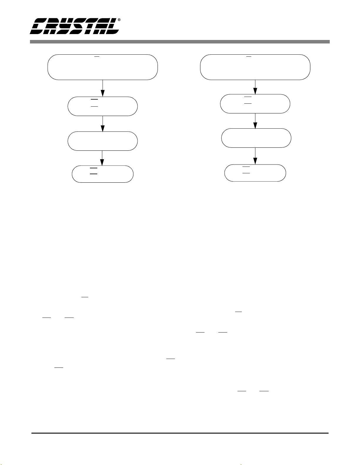
Figure 9. Motorola Mode, One-Byte Write Flow
Diagram
R/W (LOW)
CS (LOW)
WRITE BYTE TO
CS (HIGH)
DS (LOW)
ADDRESS A PARALLEL I/O REGISTER
DATA [7:0]
DS
(HIGH)
(A[1:0] SET APPROPRIATELY
R/W (HIGH)
ADDRESS A PARALLEL I/O REGISTER
(A[1:0] SET APPROPRIATELY
CS (LOW)
DS (LOW)
READ BYTE FROM
DATA [7:0]
CS
(HIGH)
DS (HIGH)
Figure 10. Motorola Mode, One-Byte Read Flow
Diagram
1) The host must drive the A1 and A0 register
address pins of the CS492X with the address of
the address of the desired Parallel I/O Register.
Host Message: A[1:0]==00b.
Host Control: A[1:0]==01b.
PCMDATA: A[1:0]==10b.
CMPDATA: A[1:0]==11b.
The host indicates that this is a write cycle by
driving the R/W pin low.
2) The host initiates a write cycle by driving the
CS and DS pins low.
3) The host drives the data byte to the DATA[7:0]
pins of the CS492X.
4) Once the setup time for the write ha s been me t,
the host ends the write cycle by driving the CS
and DS pins high.
2.2.2.2 Reading a Byte in Motorola Mode
The flow diagram shown in Figure 10 illustrates the
sequence of events that define a one-byte read in
Motorola mode.
The protocol presented Figure 10 will now be
described in detail.
1) The host must drive the A1 and A0 register
address pins of the CS492X with the address of
the desired Parallel I/O Register. Note that only
the Host Message register and the Host Control
register can be read.
Host Message: A[1:0]==00b.
Host Control: A[1:0]==01b.
The host indicates that this is a read cycle by
driving the R/W pin high.
2) The host initiates the read cycle by driving the
CS and DS pins low.
3) Once the data is valid, the host can read the
value of the selected register from the
DATA[7:0] pins of the CS492X.
4) The host should now terminate the read cycle
by driving the CS and DS pins high.
AN115REV2 21
Page 22

2.2.3 Procedures for Parallel Host Mode Communication
2.2.3.1 Control Write in a Parallel Host M ode
READ_*(HOST CONTROL REGISTER)
When writing control data to the CS492X, the same
protocol is used whether the host is writing a
control message or an entire executable download
image. Messages sent to the CS492X should be
written most significant byte first. Likewise,
downloads of the application code should also be
performed most significant byte first.
The example shown in this section can be
generalized to fit any control write situation. The
generic function ‘Read_Byte_*()’ is used in the
following example as a generalized reference to
either Read_Byte_MOT() or Read_Byte_INT(),
and ‘Write_Byte_*()’ is a generic reference to
Write_Byte_MOT() or Write_Byte_INT(). Figure
11 shows a typical write sequence.
The protocol presented in figure 11 will now be
described in detail.
1) When the host is communicating with the
CS492X, the host must verify that the DSP is
ready to accept a new control byte. If the DSP
is in the midst of an interrupt service routine, it
will be unable to retrieve control data from the
Host Message Register. Please note that
‘Read_Byte_*()’ and ‘Write_Byte_*()’ are
generic references to either the Intel or
Motorola communication protocol.
If the most recent control byte has not yet been
read by the DSP, the host must not write a new
byte.
2) In order to determine whether the CS492X is
ready to accept a new control byte the host must
check the HINBSY bit of the Host Control
YES
HINSBY==1
NO
WRITE_*(HOST MESSAGE REGISTER)
YES
Figure 11. Typical Parallel Host Mode Control
Write Sequence Flow Diagram
MORE BYTES
TO WRITE?
NO
FINISHED
Register (bit 2). If HINBSY is high, then the
DSP is not prepared to accept a new control
byte, and the host should poll the Host Control
Register again. If HINBSY is low, then the host
may write a control byte into the Host Message
Register.
3) The host knows that the DSP is ready for a new
control byte at this point and should write the
control byte to the Host Message Register
(A[1:0] = 00b).
4) If the host would like to write any more control
bytes to the CS492X, the host should once
again poll the Host Control Register (return to
step 1).
22 AN115REV2
Page 23

2.2.3.2 Control Read in a Parallel Host Mode
When reading control data from the
CS4923/4/5/6/7/8/9, the same protocol is used
whether the host is reading a single byte or a 6 byte
message.
During the boot procedure, a handshaking protocol
is used by the CS492X. This handshake consists of
a 3 byte write to the CS492X followed by a 1 byte
response from the DSP. The host must read the
response byte and act accordingly. The boot
procedure is discussed in Section 3.1 “Host Boot” -
- page 25.
INTREQ = 0
YES
READ_*(HOST CONTROL REGISTER)
NO
HOUTRDY==1
YES
During regular operation (at run-time), the
responses from the CS492X will always be 6 bytes
in length.
The example shown in this section can be used for
any control read situation. The generic function
‘Read_Byte_*()’ is used in the following example
as a generalized reference to either
Read_Byte_MOT() or Read_Byte_INT(). Figure
12 shows a typical read sequence.
The protocol presented in Figure 12 will now be
described in detail.
1) Optionally, INTREQ going low may be used as
an interrupt to the host to indicate that the
CS492X has an outgoing message. Even with
the use of INTREQ, HOUTRDY must be
checked to insure that bytes are ready for the
host during the read process. Please note that
INTREQ does not go low to indicate an
outgoing message during boot.
2) The host reads the Host Control Register
(A[1:0] = 01b) in order to determine the state of
the communication interface. Please note that
‘Read_Byte_*()’ is a generalized reference to
either Read_Byte_MOT() or Read_Byte_INT().
READ_*(HOST MESSAGE REGISTER)
YES
READ_*(HOST CONTROL REGISTER)
Figure 12. Typical Parallel Host Mode Control Read
MORE BYTES
TO READ?
NO
WAIT 100 uS
YES
HOUTRDY==1
NO
FINISHED
Sequence Flow Diagram
AN115REV2 23
Page 24

3) In order to determine whether the CS492X has
an outgoing control byte that is valid, the host
must check the HOUTRDY bit of the Host
Control Register (bit 1). If HOUTRDY is high,
then the Host Message Register contains a valid
message byte for the host. If HOUTRDY is
low, then the DSP has not placed a new control
byte in the Host Message Register, and the host
should poll the Host Control Register again.
4) The host knows that the DSP is ready to
provide a new response byte at this point. The
host can safely read a byte from the Host
Message Register (A[1:0] = 00b).
5) If the host expects to read any more response
bytes, the host should once again check the
HOUTRDY bit (return to step 1). Please refer
to one of the application code user’s guides to
determine the length of messages to read from
the CS492X. Typically this length is 1, 3 or 6
bytes, and can be deduced from the message
OPCODE.
6) After the response has been read the host
should wait at least 100 uS and check
HOUTRDY one final time. If HOUTRDY is
high once again this means that an unsolicited
message has come during the read process and
the host has another message to read (i.e. skip
back to step 4 and read out the new message).
24 AN115REV2
Page 25

3. BOOT PROCEDURE & RESET
In this section the process of booting and
downloading to the CS492X will be covered as
well as how to perform a soft reset. Both host boot
and autoboot are covered in this section.
3.1 Host Boot
A flow diagram of a typical serial download
sequence and a typical parallel download sequence
will be presented, as well as pseudocode
representing a download sequence from the
programmers perspective. The pseudocode is
written in a general sense where function calls are
made to Write_* and Read_*. The * can be
replaced by I2C, SPI, INTEL, or MOTO depending
on the mode of host communication. For each case
the general download algorithm is the same.
The download and boot procedure is accomplished
with RESET (pin 36), and the communication pins
discussed in Section 2.1 “Serial Communication” -
- page 8. The flow diagrams in Figures 13 and 14
illustrate a typical boot and download procedure.
Table 7 defines the boot write messages and Table
8 defines the boot read messages in mnemonic and
actual hex value. These messages will be used in
the boot sequence.
2) The host should then send the boot message
DOWNLOAD_BOOT (0x000004). This
causes the CS492X to initialize itself for
download.
3) If the initialization was successful the CS492X
sends out the boot message BOOT_START
(0x01) and the host should proceed to step 5.
MNEMONIC VALUE
SOFT_RESET 0x000001
RESERVED 0x000002
RESERVED 0x000003
DOWNLOAD_BOOT 0x000004
BOOT_SUCCESS_RECEIVED 0x000005
Table 7. Boot Write Messages
MNEMONIC VALUE
BOOT_START 0x01
BOOT_SUCCESS 0x02
APPLICATION_FAILURE 0xF0
BOOT_ERROR 0xFA
INVALID_MSG 0xFB
BOOT_ERROR 0xFC
INIT_FAILURE 0xFD
INIT_FAILURE 0xFE
BAD_CHECKSUM 0xFF
Table 8. Boot Read Messages
The following is a detailed description of a
download sequence for the CS492X. All writes and
reads with the CS492X should follow the protocol
given in Section 2 “Host Communication” -- page
8, and timing given in the CS492X Datasheet.
NOTE: When reading from the chip in a serial
communication mode, the host must wait for the
interrupt request (INTREQ) to fall before starting
the read cycle.
1) A download sequence is started when the host
issues a hard reset and holds the mode pins
appropriately (WR, RD, and PSEL) as described
in Section 2 “Host Communication” -- page 8
and in the CS492X Datasheet. It is assumed that
timing is satisfied as per the CS492X Datasheet.
AN115REV2 25
4) If initialization fails, the CS492X sends out an
INIT_FAILURE boot message byte (0xFD or
0xFE), INVALID_MSG byte (0xFB), or
BOOT_ERROR byte (0xFA or 0xFC) and
spins waiting for a hard reset. The host should
re-try steps 1 through 3 and if failure is met
again, the serial communication timing and
protocol should be inspected.
5) After receiving the BOOT_START byte, the
host should write the downloadable image
(from the .LD file).
6) The end of the .LD file contains a three byte
checksum. If the checksum is good after
download, the CS492X will send a
BOOT_SUCCESS message (0x02) to the host.
Page 26

RESET(LOW) (NOTE 1) RESET(HIGH) (NOTE 2) WAIT 500 NS
WRITE_*(DOWNLOAD_
BOOT, MSG_SIZE)
INTREQ LOW?
Y
READ_*(MESSAGE)
MESSAGE ==
BOOTSTART?
Y
WRITE_*(.LD FILE,
DOWNLOAD FILE SIZE)
INTREQ LOW?
Y
READ_*(MESSAGE)
N
TIMEOUT AFTER
20MS (NOTE 3)
Notes: 1. RESET
least 100 ns to satisfy t
must be held LOW for at
rstl
2. It sho uld be noted that mode pins
are used to configure the CS492X
serial communication mode.
These mode pins are latched
internally on the rising edge of
reset. The pins can be set
dynamically by a microprocessor
N
EXIT(ERROR)
or can be statically pulled HIGH or
LOW. If these pins are driven
dynamically, setup and hold times
must be satisfied as stated in the
CS492X datasheet. More
information about the function of
the mode pins can be found in the
CS492X datasheet and in Section
2 “Host Communication” -- page 8.
3. Time-out values reflect worst case
response time for the CS492X.
The values shown may be us ed for
N
TIMEOUT AFTER
20MS (NOTE 3)
the host’s time-out control loop.
4. Hardware configuration messages
are covered in Section 5
“.Hardware Configuration” -- page
46. Application configuration
messages are covered in each
application code user’s manual.
MESSAGE ==
BOOT_SUCCESS?
Y
WRITE_*(BOOT_
SUCCESS_RECEIVED,
MSG-SIZE)
N
EXIT(ERROR)
WAIT 5 MS
DOWNLOAD COMPLETE
WRITE_*(CONFIGURATION_
MESSAGES, CONFIG_
MSG_SIZE) (NOTE 4)
Figure 13. Typical Serial Boot and Download Procedure
26 AN115REV2
Page 27

RESET(LOW) (NOTE 1) RESET(HIGH) (NOTE 2) WAIT 500 NS
CONTROL_WRITE_*(DOWNLOAD_
BOOT, MSG_SIZE)
HOUTRDY HIGH?
Y
READ_*(MESSAGE)
MESSAGE ==
BOOTSTART?
Y
CONTROL_WRITE_*(.LD FILE,
DOWNLOAD FILE SIZE)
HOUTRDY HIGH?
Y
READ_*(MESSAGE)
N
N
N
TIMEOUT AFTER
20MS (NOTE 3)
EXIT(ERROR)
TIMEOUT AFTER
20MS (NOTE 3)
Notes: 1. RESET
least 100 ns to satisfy t
2. It sho uld be noted that mode pins
are used to configure a CS492X
parallel communication mode.
These mode pins are latched
internally on the rising edge of
reset. The pins can be set
dynamically by a microprocessor
or can be statically pulled HIGH or
LOW. If these pins are driven
dynamically, setup and hold times
must be satisfied as stated in the
CS492X Datasheet. More
information about the function of
the mode pins can be found in the
CS492X Datasheet and in Section
2 “Host Communication” -- page 8.
3. Time-out values reflect worst case
response time for the CS492X.
The values shown may be used fo r
the host’s time-out control loop.
4. Hardware configuration messages
are covered in Section 5
“.Hardware Configuration” -- page
46. Application configuration
messages are covered in each
application code user’s manual.
must be held LOW for at
rstl
MESSAGE ==
BOOT_SUCCESS?
Y
CONTROL_WRITE_*(BOOT_
SUCCESS_RECEIVED,
MSG-SIZE)
N
EXIT(ERROR)
WAIT 5 MS
DOWNLOAD COMPLETE
CONTROL_WRITE_*(CONFIGURATION_
MESSAGES, CONFIG_MSG_SIZE)
(NOTE 4)
Figure 14. Typical Parallel Boot and Download Procedure
AN115REV2 27
Page 28

3.3V
8
3.3V
EMAD[7:0] DA TA [7:0]
CS4923/4/5/6/7/8/9
HOST
uCONTROLLER
ABO OT is an open-drain pin which requires
the pull-up shown.
ABOOT and INTREQ are multiplexed onto
the same pin. Therefore the host should
drive ABOOT with an open-drain driver.
ABOOT
RESET
Figure 15. Autoboot Memory Architecture
EMOE
EXTMEM
EMWR
If the checksum was bad, the CS492X responds
with the BAD_CHECKSUM message byte
(0xFF) and spins, waiting for hard reset.
7) After reading out the BOOT_SUCCESS byte,
the host should send the
BOOT_SUCCESS_RECEIVED message
(0x000005) which will cause an internal
application code reset and allow the
downloaded application to run.
3.3V
3.3V 3.3V
R1 R3
R2 R4
DQ
8 BIT
'574
DFF
Only one of R1 and R2 should be stuffed.
Only one of R3 and R4 should be stuffed.
The state of EMOE and EMWR at the
rising edge of RESET will determine the
serial mode that the part comes up in
while using external memory. Please see
the Serial Communication section for
more details.
ADDR[7:0]
ADDR[15:8]
DQ
8 BIT
'574
DFF
ADDR[7:0]
ADDR[15:8]
OE
64K X 8
CS
ROM
3.2 Autoboot
Autoboot is a feature available on all DSPs in the
CS492X family which gives the decoder the ability
to load application code into itself. Because
external memory is accessed with the 8-bit GPIO
interface, autoboot restricts host control to serial
communication. Figure 15 shows that an autoboot
system can be built with a CS492X decoder, two
octal latches and an external ROM.
8) After waiting 5ms to allow the downloaded
application to initialize, the host can send
configuration messages for both hardware and
software configuration. The hardware
configuration messages are described in
Section 5 “.Hardware Configuration” -- page
46. For more information about software
application messages please refer to the
Application Code User’s Guide for the code(s)
that are being used.
The pseudocode in Section 6.3 “Typical Download
Session with the CS4923/4/5/6/7/8/9” -- page 64
demonstrates a typical serial host download session
with the CS492X.
In this system RESET and ABOOT are the control
pins which are used to initiate autoboot. It is
important to be aware that the ABOOT pin also
serves as the INTREQ pin for the decoder, which
means that it will be driven by the decoder when
out of the reset condition. Due to this constraint,
ABOOT should be connected to an open-drain
output of the microcontroller so as to allow the
specified pull-up resistor to generate the high
value. At the completion of a successful download
INTREQ (ABOOT) becomes an output and the
host should no longer drive it.
The EMAD[7:0] pins serve as a multiplexed data
and address bus. Note that the pins are connected to
28 AN115REV2
Page 29

RESET
ABOOT
EXTMEM
EMOE
EMWR
EMAD7:0 MA23:16 MA15:8 MA7:0 Data7:0
Figure 16. Autoboot Timing Diagram
both the input of the first latch, and the output of the
ROM. The two latches are cascaded such that on
each clock pulse a new address byte is latched into
the first latch, and the previous ADDR[7:0] byte is
latched into the second register becoming
ADDR[15:8].
The timing for an autoboot sequence is illustrated
in Figure 16. The sequence is initiated by driving
RESET low and placing the decoder into a reset
state. At the rising edge of RESET the ABOOT,
WR, and RD pins are sampled. If ABOOT is low
when sampled, and the WR and RD pins are set to
configure the device for serial communications, the
device will begin to autoboot. Section 2.1 discusses
the procedure required for placing the CS492X into
a serial communication mode. For a more thorough
description of ABOOT’s behavior after the rising
edge of RESET please see section 3.2.1
The EMOE pin of the CS492X is used for two
purposes. It generates clock pulses for the latches,
and it is used in conjunction with EXTMEM to
enable the outputs of the ROM. The first three
rising edges of EMOE are used to latch address
bytes, as shown in the diagram. The fourth low
pulse of EMOE is used to enable the ROM outputs.
When both EXTMEM and EMOE go low, the
EMAD[7:0] pins of the DSP become inputs and
await the data coming from the ROM.
When comparing the memory syste m in Fi gure 15
to the timing diagram of Figure 16 there may
appear to be a discrepancy. The timing diagram
shows three address cycles, but there are only two
latches in the illustration of the memory
architecture. This difference is a result of code size
limitations. The application code is guaranteed to
fit into a 32 Kilobyte space, which means that only
15 address bits will actually be used for retrieving
code from the ROM. Thus, the two latches catch
the least significant bytes, and the most significant
byte is dropped.
In autoboot mode, latching the most significant
byte would be perfectly valid since the most
significant bits are guaranteed to be zeros (the three
bytes represent a true 24-bit address). If the
external memory is to be used for access during
run-time (such as in DTS decode), however, a third
latch would break the memory interface. Different
external memory inte rface schemes are discussed
in more detail in Section 4.
The flow chart given in Figure 17 demonstrates the
interaction required by the microcontroller when
placing the DSP into autoboot mode. The host must
first drive the RESET line low. The host also drives
ABOOT low and hold it in a low state until the
rising edge of RESET. The low state of ABOOT at
the rising edge of RESET initiates autoboot. As
noted on the diagram, the host control mode must
be configured for serial communications, and the
appropriate setup (T
) and hold (T
rstsu
rsthld
) times
must be observed.
AN115REV2 29
Page 30

RESET
ABOOT
(LOW) (NOTE 1)
(LOW)
RESET(HIGH) (NOTE 2)
ABOOT(HIGH)
WAIT 175 MS
READ_*(VARIABLE)
CORRECT VALUE?
AUTOBOOT COMPLETE
WRITE_*(HW_CONFIG_MSG,
WRITE_*(SW_CONFIG_MSG,
WRITE_*(KICKSTART,
(NOTE 3)
(NOTE 4)
Y
HW_MSG_SIZE)
(NOTE 4)
SW_MSG_SIZE)
(NOTE 4)
MSG_SIZE)
(NOTE 4)
N
WAIT 5 MS
Notes: 1. RESET
satisfy the T
Datasheet.
2. The RD
serial communication mode as defined in the
CS4923/4/5/6/7/8/9 Datasheet. The setup (T
ns) and hold (T
for the RD
3. INTREQ
4. The READ_* and WRITE_* functions are
placeholders for the READ_I2C/READ_SPI and
WRITE_I2C/WRITE_SPI functions defined in the
Serial Communication section.
must be held LOW for at least 100 ns to
as specified in the CS4923/4/5/6/7/8/9
rstl
and WR pins must be configured to select a
= 50
= 15 ns) times must be observed
rsthld
rstsu
, WR, and AUTOBOOT pins.
should be ignored during this period.
Figure 17. Autoboot Sequence
30 AN115REV2
Page 31

Because ABOOT must be driven by the host with
an open-drain pin, the statement ABOOT(HIGH)
should be understood to mean
ABOOT(RELEASE). The pull-up resistor required
on the ABOOT (or INTREQ) line will always be
responsible for producing a high value on the pin.
ABOOT should never be driven high by the host.
After waiting for 175ms, the download should have
completed. During the wait period, the host should
ignore all INTREQ behavior (mask the INTREQ
interrupt). The host can then verify that the code
has successfully initialized itself by reading a
variable from the application and checking the
returned value against the known default value.
Any variable can be used for the verification step,
but a robust design will select a variable whose
value is neither all 0’s nor all 1’s. If the first read
attempt returns an incorrect value, a 5ms wait
should be inserted and the read should be repeated.
If a second invalid number is read, the entire boot
process should be repeated. When the number
returned matches the default value for the variable
read, the host can be confident that the application
is resident in the DSP and awaiting further
instruction.
Hardware configuration messages are used to
define the behavior of the DSP’s audio ports. A
more detailed description of the different hardware
configurations can be found in the Section 5
“.Hardware Configuration” -- page 46.
The software configuration messages are specific
to each application (AC-3, MPEG, Crystal Origina l
Surround, and DTS). The user’s guide for each
application provides a list of all pertinent
configuration messages. Writing the KICKSTART
message to the CS492X begins the audio decode
process. The KICKSTART message will also be
described in the user’s guide for each application.
Until the KICKSTART has been sent, the decoder
is in a wait state.
3.2.1 Autoboot INTREQ Behavior
It is important to note that ABOOT and INTREQ
are multiplexed on pin 20 of the CS492X. Because
this pin serves as an input before reset, and an
output after reset, the host should release the
ABOOT line after RESET has gone high. As
shown in Figure 18, the host must drive ABOOT
low around the rising edge of RESET, while
observing the T
given in the CS492X Family Data Sheet in order to
initiate an autoboot sequence.
After the host has released the ABOOT line, it will
remain high while the DSP prepares to load code
into itself. When the DSP has begun the boot
process INTREQ (ABOOT) will be driven low and
it will remain low during the entire download
procedure. INTREQ should be ignored during
download, i.e. interrupts should be masked on the
host. The download time will vary according to the
size of the download image and the frequency of
rstsu
and T
timing parameters
rsthld
T
rstsu
RESET
ABOOT
T
rsthld
Figure 18. Autoboot INTREQ Behavior
AN115REV2 31
Download in Progress
Driven Low by Host
Driven Low by CS492X
Page 32

the main DSP clock. At the conclusion of autoboot,
the DSP issues an internal reset which will cause
INTREQ to rise, indicating that boot has
completed. The autoboot sequence is guaranteed to
complete in 175ms (from rising edge of RESET to
the internal reset of the CS492X).
3.3 Application Failure Boot Message
Each piece of application code is specifically
tailored for either the CS4923, CS4924, CS4925,
CS4926, CS4927, CS4928 or CS4929. Although it
is possible to load a piece of code into the wrong
chip and receive a BOOT_SUCCESS byte, the
code will not initialize itself. In order to facilitate
the debug of designs which can accept many
members of the CS492X family, an
APPLICATION_FAILURE message is provided.
As mentioned earlier, the host should wait for at
least 5ms after download before sending
configuration messages to the CS492X. This
provides time for the code to initialize itself. If the
INTREQ pin is low 1ms after the download process
has completed, the host should read from the
CS492X. The byte 0xF0 indicates
APPLICATION_FAILURE. This byte informs the
host that the application code was loaded into an
incompatible DSP. As an example, loading DTS
application code into the CS4923 will generate an
APPLICATION_FAILURE byte.
Although most boot messages are essentially
ignored for autoboot, it should be noted that the
APPLICATION_FAILURE message is applicable
whether serial boot or autoboot is used.
3.4 Resetting the CS4923/4/5/6/7/8/9
Resetting the CS492X uses a combination of
software and hardware. To reset the device, a
previous application must have been downloaded.
The flow diagram in Figure 19 shows the procedure
for performing a reset.
RESET(LOW) (NOTE 1)
RESET(HIGH) (NOTE 2)
WAIT 500 ns
WRITE_* (SOFTRESET,
MSG_SIZE)
WAIT 5 ms
WRITE_*
(CONFIGURATION_MESSAGES,
CONFIG_MSG_SIZE)
(NOTE 3)
Notes: 1. RESET must be held LOW for at least 100 ns to satisfy
t
rstl
2. It should be noted that mode pins are used to configure
the CS492X communication mode. These mode pins
are latched internally on the rising edge of reset and
can be set dynamically by a micropro cessor or can be
statically pulled HIGH or LOW. If these pins are driven
dynamically, setup and hold times must be satisfied as
stated in the CS492X Datasheet. More information
about the function of the mode pins can be found in the
CS492X Datasheet and in Section 2 “Host
Communication” -- page 8,
3. Configuration messages determine both hardware and
software configuration. Hardware configurations are
described in section 5 of this manual. Software
application configuration messages are described in
the Application Code User’s Guide for the code being
used.
Figure 19. Performing a Reset
32 AN115REV2
Page 33

The following is a detailed description of a reset
sequence to the CS492X. All writes and reads with
the CS492X should follow the protocol given in
Section 2 “Host Communication” -- page 8, and
timing given in the CS492X Datasheet.
1) Reset begins when the host issues a hard reset
and holds the mode pins appropriately (WR,
RD, and PSEL) as described in Section 2 “Host
Communication” -- page 8 and in the CS492X
Datasheet. It is assumed that the
communication protocol is followed for
whichever communication mode is chosen by
the host and that timing is satisfied per the
CS492X Datasheet.
2) The host should then send the message
SOFT_RESET (0x000001). This will restart
the previously downloaded application with all
of the hardware configurations in their default
states. The Application Code User’s Guide for
each application lists those parameters which
are affected by a SOFT_RESET.
3) After waiting 5 ms to allow the downloaded
application to initialize, the host can send
configuration messages for both hardware and
software configuration. Hardware configuration
messages are described in Section 5
“.Hardware Configuration” -- page 46.
Software application configuration messages
are described in the Application Code User’s
Guide for the code being used.
The pseudocode in Section 6.4 “Typical Reset
Sequence for the CS4923/4/5/6/7/8/9” -- page 65
demonstrates a typical reset sequence for the
CS492X.
AN115REV2 33
Page 34

4. EXTERNAL MEMORY
The CS492X family of DSPs provide a byte-wide
interface for accessi ng external memory. The basic
memory interface is implemented with the following
pins: EMAD[7:0], EXTMEM, EMOE, and EMWR.
Each pin has been described in Table 9.
The host communication mode is important when
considering the external memory interface.
External memory can only be connected to those
systems which implement a serial control host
interface. Any systems using the parallel host
cannot use the external memory interface.
The entire family of decoders has the capability of
autobooting, as discussed in Section 3.2 External
memory is used to hold the application code that
the DSP will load into itself. Because the CS4923,
CS4924, CS4925 and CS4929 do not require
Autoboot capability, external memory is optional.
The CS4926 and CS4928, however, require the use
of external memory. An external ROM must be
used for holding the DTS look-up tables employed
by the CS4926 and CS4928 during the decode of a
DTS bit-stream. Table 10 lists the memory
configurations for each decoder.
In a simple system, a non-paged memory can be
used to hold a single piece of autoboot code or the
DTS tables alone (e.g., the CS4928). In more
complex systems, a paged memory architect ure can
be used to hold multiple pieces of application code
and the DTS tables (e.g., the CS4926). Both
memory architectures, paged and non-paged, will
be presented in detail later in this section.
Pin Name Pin Number Pin Function
EMAD0 17 Multiplexed Address and Data Bit 0
EMAD1 16 Multiplexed Address and Data Bit 1
EMAD2 15 Multiplexed Address and Data Bit 2
EMAD3 14 Multiplexed Address and Data Bit 3
EMAD4 11 Multiplexed Address and Data Bit 4
EMAD5 10 Multiplexed Address and Data Bit 5
EMAD6 9 Multiplexed Address and Data Bit 6
EMAD7 8 Multiplexed Address and Data Bit 7
EXTMEM
EMOE
EMWR
* - These pins must be configured appropriately to select a serial host communication mode for the
CS4923/4/5/6/7/8/9 at the rising edge of RESET
Part Number Host Control Mode if using External ROM Memory Usage
CS4923,4,5,7,9
CS4926,8
Table 10. Memory and Control Requirements for the CS4923/4/5/6/7/8/9 Family
21 External Memory Select
5 * External Memory Output Enable &Address Latch Strobe
4 * External Memory Write Strobe
Table 9. Memory Interface Pins
2
I
C or SPI
2
C or SPI
I
OPTIONAL – Autoboot mode
REQUIRED – DTS Tables
OPTIONAL – Autoboot mode
34 AN115REV2
Page 35

4.1 Basic Memory Architecture
serial mode that
while using exter
section 2,
The simplest external memory system consists of the
DSP’s memory interface, the external memory, and
two octal latches to hold the memory address. This
configuration is a non-paged memory architecture,
and a block diagram of this system is shown in
Figure 20. Non-paged memories are ideal for
autobooting a single piece of application code such
as AC-3. Because the application code is guaranteed
to fit within a 32 Kilobyte space, it is only necessary
to provide 15 address bits. The 16th address bit
coming from the DSP may, however, be connected
to the memory since the most significant bit is
guaranteed to always be 0 during autoboot. Figure
21 shows the functional timing of an autoboot
sequence in which three address cycles are
illustrated. Due to the code size limitati on, however,
only the lower 15 bits of this address are relevant.
The CS4926 and CS4928 both have special
memory requirements since they must access lookup tables while processing DTS encoded audio.
These tables will reside in a 64 Kilobyte page of
external memory. The memory architecture
illustrated in Figure 20 is also applicable for the
3.3V
8
EMAD[7:0] DAT A[7:0]
CS4923/4/5/6/7/8/9
EMOE
EXTMEM
EMWR
3.3V
3.3V 3.3V
R1 R3
R2 R4
DQ
ADDR[7:0]
8 BIT
DQ
'574
8 BIT
DFF
'574
DFF
Only one of R1 and R2 should be stuffed.
Only one of R3 and R4 should be stuffed.
The state of EMOE and EMWR at the
rising edge of RESET will determine the
Serial Communication for
more details.
ADDR[7:0]
ADDR[15:8]
ADDR[15:8]
OE
64K X 8
CS
ROM
the part comes up in
nal memory. Please see
Figure 20. Basic Memory Architecture
DTS tables since only 16 bits are necessary for
addressing all 64 Kilobytes. The timing
requirements for the memory used in a DTS
system, however, are different from the timing
requirements of the memory used for autoboot
only. Accesses made during run-time occur at a
higher frequency, and there are only two a ddress
cycles as can be seen in Figure 22. Consequently, a
DTS system requires a faster ROM.
RESET
ABOOT
EXTMEM
EMOE
EMWR
EMAD7:0 MA23:16 MA15:8 MA7:0 Data7:0
Figure 21. Autoboot Timing Diagram
Figure 22. Run-Time Memory Access
AN115REV2 35
Page 36

Table 11 lists the memory speed requirements
based on the ROM content.
ROM Content ROM Speed
AUTOBOOT Code 330ns
DTS Tables Only 110ns
AUTOBOOT Code & DTS
Tables
Table 11. ROM Speeds
1 10ns
4.2 Non-Paged Memory
A non-paged memory architecture should be used in
systems which will need to access 64 Kilobytes of
data or less. One example of such a system would be
a decoder designed for AC-3 autoboot only. In this
case the only code ever needed would be the
application code that would run on the CS4923 or the
CS4924. The code is constrained to occupy less than
32 Kilobytes of memory, which means that only 15
bits would be required to access the entire image.
Therefore a single-code autoboot system could use
the 16-bit addressing scheme shown in Figure 20.
Another possible scenario is a CS4926 or CS4928
DTS decoder which will be booted by the host. In this
system only a 64 Kilobyte ROM would be necessary
for holding the look-up tables. Once again, the basic
memory architecture presented in Figure 20 would be
adequate.
The DSP always considers its address space to range
from 0x0000 to 0xFFFF. This means that the d ecoder
is unaware of any data which falls outside of these 64
Kilobytes. In autoboot mode there is yet another
constraint – the autoboot process always begins with
address 0x0000. The implication is that the host
microcontroller must somehow be involved in
memory accesses which exceed the 64 Kilobyte
scope of the CS492X, and the host must also manage
access to all pieces of autoboot code which do not
physically reside at location 0x0000. The limitations
of a non-paged memory are easily seen, and they can
be circumvented using paged memory designs as
discussed in the next section.
4.3 Paged Memory
A paged memory architecture is necessary for
those systems which provide autoboot for multiple
code loads (e.g. when using Autodetect), or in any
CS4926 or CS4928 system which utilizes autoboot.
Paged memory is defined as a large memory
partitioned into smaller blocks. The easiest
partitioning scheme for the CS4923/4/5/6/7/8/9
family is on 64 Kilobyte boundaries because of the
sixteen bits of address provided by the DSP. If
memory space is at a premium, and the system
under design does NOT use the CS4926 or the
CS4928, it is possible to perform paging on 32
Kilobyte boundaries.
The host microcontroller plays a crucial role in
paged memory systems, since it is directly
responsible for addressing each page. In a memory
composed of 64 Kilobyte pages, the high order
address bits of the ROM, A16 and A17, would be
controlled directly by the microcontroller as shown
in Figure 23. These two address lines give the host
the capability to select any of four 64 Kilobyte
pages in memory.
A memory with 32 Kilobyte pages can be used only
to hold autoboot code. Such a memory would be
paged with bits A15 and A16. Using this design
template, it is vital that the most signifi cant address
bit latched from the DSP, A15, not be connected to
the memory. The host microcontroller is
responsible for controlling address bits A15 and
greater. A 32 Kilobyte design is presented in Figure
24.
The main variable in organizing the ROM is the
page size. The easiest way to determine the page
size for your system is to look at the largest block
of memory required for any operation. If the
external ROM is designed to hold only autoboot
code, the designer has the option of using either 32
Kilobyte or 64 Kilobyte pages. The final decision
would depend upon the size of the memory which
will be used in the final design.
36 AN115REV2
Page 37

serial mode that
while using exter
section 2,
3.3V
serial mode that
while using exter
section 2,
8
EMAD[7:0] DA T A[7:0]
CS4923/4/5/6/7/8/9
EMOE
EXTMEM
EMWR
Figure 23. External Memory with 64 Kilobyte Pages
3.3V
ADDR[7:0]
ADDR[15:8]
DQ
uCADDR16**
8 BIT
'574
uCADDR17**
DFF
the part comes up in
nal memory. Please see
Serial Communication for
R1 R3
R2 R4
DQ
8 BIT
'574
DFF
Only one of R1 and R2 should be stuffed.
Only one of R3 and R4 should be stuffed.
The state of EMOE and EMWR at the
rising edge of RESET will determine the
more details.
3.3V
3.3V 3.3V
**The address lines uCADDR16 and uCADDR17 should come
from an external microcontroller and be used to page t he
memory for the CS4923/4/5/6.
ADDR[7:0]
ADDR[15:8]
ADDR16
ADDR17
OE
256K X 8
CS
ROM
8
EMAD[7:0] DA T A[7:0]
CS4923/4/5/7/9
EMOE
EXTMEM
EMWR
ADDR[7:0]
ADDR[14:8]**
DQ
uCADDR15**
8 BIT
'574
uCADDR16**
DFF
the part comes up in
nal memory. Please see
Serial Communication for
R1 R3
R2 R4
DQ
8 BIT
'574
DFF
Only one of R1 and R2 should be stuffed.
Only one of R3 and R4 should be stuffed.
The state of EMOE and EMWR at the
rising edge of RESET will determine the
more details.
3.3V
3.3V 3.3V
**The address lines uCADDR15 and uCADDR16 should come from an
extern al microcontroller and be used to page the memory for the
CS4923/4/5/7/9. The high order bit from the second D flip flop should be left
as a no connect to allow for an external microcontroller to drive ADDR1 5 of
the memory. Because the CS4923/4/5/7/9 will not drive ADDR15, only
ADDR[14:8] should be connected from the second D flip flop to the
memory.
ADDR[7:0]
ADDR[14:8]
ADDR15
ADDR16
OE
128K X 8
CS
ROM
Figure 24. External Memory With 32 Kbyte Pages
AN115REV2 37
Page 38

ROM Content Image Size Number of Pages Required Recommended Page Size
CS4923
AC-3 32 Kbytes 1 Non-Paged
AC-3,Crystal Original Surround 32 + 32 = 64 Kbytes 2 32 Kbytes or 64 Kbytes
CS4924
AC-3 32 Kbytes 1 Non-Paged
AC-3 with Q-Sound 32 Kbytes 1 Non-Paged
CS4925
AC-3, MPEG Multi-Channel,
Crystal Original Surr ou n d
CS4926
DTS Tables 64 Kbytes 1 Non-Paged
DTS Tables, DTS, AC-3, Crystal
Original Surroun d
CS4927
MPEG Multi-Channel 32 Kbytes 1 Non-Paged
MPEG Multi-Channel, Crystal
Original Surroun d
CS4928
DTS Tables 64 Kbytes 1 Non-Paged
DTS Tables, DTS, Crystal
Original Surroun d
CS4929
AAC 2-Channel 32 Kbytes 1 Non-Paged
AAC 2-Channel, MPEG Stereo 32 + 32 = 64 Kbytes 2 32 Kbytes or 64 Kbytes
32 + 32 + 32 =
96 Kbytes
64 + 32 + 32+ 32 =
160 Kbytes
32 + 32 = 64 Kbytes 2 32 Kbytes or 64 Kbytes
64 + 32 + 32 =
128 Kbytes
Table 12. External Memory Configurations
3 32 Kbytes or 64 Kbytes
4 64 Kbytes
3 64 Kbytes
A system using a CS4926 or CS4928, however,
will always require a 64 Kilobyte page for the DTS
look-up tables. Thus, the most straightforward
externally paged ROM for an autobooting CS4926
memory more efficiently in a DTS system. The
examples also include several figures which
present the different ROM configurations as
composite memory images.
or CS4928 would have 64 Kilobyte pages. The
CS4926 or CS4928 would control the lowest
sixteen bits of address, and the host microcontroller
would control the most significant address bits.
Table 12 lists possible external memory
configurations for each DSP. The table provides a
list of the ROM content, the size of the combined
memory images, the recommended page size, and
the number of discrete pages required. The page
sizes were calculated using the methodology
discussed previously. A more complex memory
scheme is given in the CRD4923-MEM example
(Figure 32), which demonstrates how to pack the
38 AN115REV2
4.4 Examples
4.4.1 Non-Paged Memory
The most rudimentary memory design discussed
above is the non-paged memory. In a non-paged
design, the DSP can only access one item in
memory which could be either a single autoboot
code load, or the DTS tables for the CS4926 or
CS4928. The memory image given in Figure 25 is
an example of a non-paged memory image.
The memory image shown above would be
designed into a system using the memory
architecture laid out in Figure 20. All 16 output bits
Page 39

0x00000
Figure 25. Non-Paged Memory
AC-3 Cod e
or
0x0FFFF
DTS T a b le s
of the address latches would be connected to
address bits A0-A15 of the external ROM. The host
is completely isolated from memory accesses in
this situation. Once the hardware has been
designed, the DSP itself will be responsible for all
communication with the ROM.
4.4.2 32 Kilobyte Paged Autoboot Memory
An external memory architecture which is paged
on 32 Kilobyte boundaries will necessarily contain
only autoboot code. Therefore, this architecture can
only be used by the CS4923/4/5/7/9. Because of the
64 Kilobyte look-up table that must be used during
the decode of a DTS stream, the CS4926 and
CS4928 could never be used with a fixed
32 Kilobyte page size. Figure 26 shows an example
of a 32 Kilobyte paged memory image.
The flow diagram given in Figure 27 demonstrates
the interaction required by the microcontroller
during autoboot. After placing the decoder into a
reset state, the host selects the page in memory
containing AC-3 Code by driving uC15 to a low
state. The host also drives ABOOT low and holds
it in a low state until the rising edge of RESET to
initiate autoboot. As noted in the autoboot section,
the ABOOT pin should be connected to an opendrain output of the microcontroller so as to allow
the specified pull-up resistor to generate the high
0x00000
AC-3 Code
0x07FFF
0x08000
Crystal Original
Surround Code
0x0FFFF
Addres s line A15
used for paging
Figure 26. 32 Kbyte Paged memory
value. The open-drain driver is required because
the DSP will begin using the pin as an output after
a successful download (INTREQ and ABOOT are
multiplexed on the same pin).
After waiting for 175 ms the download should have
completed. During the wait period, the host should
ignore all INTREQ behavior (mask the INTREQ
interrupt). The host can then verify that the code
has successfully initialized itself by reading a
variable from the application and checking the
returned value against the default value. Any
variable can be used for the verification step, but a
robust design will select a variable whose value is
neither all 0’s nor all 1’s. If the first read attempt
returns an incorrect value, a 5 ms wait should be
inserted and the read should be repeated. If a
second invalid number is read, the entire boot
process should be repeated. When the number
returned matches the default value for the variable
read, the host knows that the application is resident
in the DSP and awaiting further instruction. Please
see Section 3.2 “Autoboot” -- page 28 for more
information.
AN115REV2 39
Page 40

Correct Value?
Y
N
Wait 5 ms
RESET (LOW)
ABOOT (LOW)
uC15 (LOW)
RESET (HIGH)
Address AC-3 Code
READ_*(Variable)
†
Wait 175 ms
Ignore
INTREQ
Autoboot Complete
WRITE_*(HW_CONFIG_MSG,
HW_MSG_SIZE)
†
WRITE_*(SW_CONFIG_MSG,
SW_MSG_SIZE)
†
WRITE_*(KICKSTART,
MSG_SIZE)
†
†
The READ_* and WRITE_* functions are placeholders
for the READ_I2C/READ_SPI and WRITE_I2C/
WRITE_SPI functions defined in the Serial
Communications section.
Figure 27. Autoboot Sequence for 32 Kbyte
Paged Memory
ABOOT (HIGH)
4.4.3 64 Kilobyte Paged Autoboot Memory
Systems using fixed page sizes can implement either
64 Kilobyte or 32 Kilobyte pages when the audio
decoder is one of the CS4923/4/5/7/9, but the
CS4926 and CS4928 are restricted to 64 Kilobyte
pages. The larger page size adds more versatility to
the system design because both autoboot code and
DTS tables can be included in any external ROM
utilizing 64 Kilobyte pages. The next two examples
show possible memory designs. The first memory
image contains only autoboot code, and the second
example shows an external ROM image which holds
multiple pieces of autoboot code in addition to the
DTS look-up tables.
The memory image illustrated in Figure 28 is
designed for a system using external ROM for
autoboot purposes only. There are only two pages to
choose from, which means that the host
microcontroller needs to drive one memory address
line. In this case, it would be bit A16. The
architecture for this memory c onfigurati on is shown
in Figure 23. All 16 bits of latched address are
connected to the memory, and the microcontroller
would provide uC16 for paging between the AC-3
Code and Crystal Original Surround.
The flow diagram given in Figure 29 demonstrates
the interaction required by the microcontroller when
placing the DSP into autoboot mode. After placing
the decoder into a reset state, the host selects the
page in memory containing Crystal Original
0x00000
AC-3 Code
0x0FFFF
0x10000
Crystal Ori ginal
Surround Code
0x1FFFF
Address line A16
used for paging
Figure 28. 64 Kbyte Paged Autoboot Memory
40 AN115REV2
Page 41

Surround Code by driving uC16 to a high state. The
host also drives ABOOT low and holds it in a low
state until the rising edge of RESET to initiate
autoboot. As noted in the autoboot section, the
ABOOT pin should be connected to an open-drain
output of the microcontroller so as to allow the
specified pull-up resistor to generate the high value.
The open-drain driver is required because the DSP
will begin using the pin as an output after a
successful download (INTREQ and ABOOT are
multiplexed on the same pin).
After waiting for 175 ms the download should have
completed. During the wait period, the host should
ignore all INTREQ behavior (mask the INTREQ
interrupt). The host can then verify that the code has
successfully initialized itself by reading a variable
from the application and checking the returned value
against the default value. Any variable can be used
for the verification step, but a robust design will
select a variable whose value is neither all 0’s nor all
1’s. If the first read attempt returns an incorrect
value, a 5 ms wait should be inserted and the read
should be repeated. If a second invalid number is
read, the entire boot process should be repeated.
When the number returned match es the default value
for the variable read, the host knows that the
application is resident in the DSP and awaiting
further instruction. Please see Section 3.2
“Autoboot” -- page 28 for more information.
RESET (LOW)
ABOOT (LOW)
uC16 (HIGH)
Address Crystal
Surround Sound
RESET (HIGH)
ABOOT (HIGH)
Wait 175 m s
Ignore
INTREQ
READ_*(Variable)
Correct Value?
Autoboot Complete
WRITE_*(HW_CONFIG_MSG,
HW_MSG_SIZE)
WRITE_*(SW_CONFIG_MSG,
SW_MSG_SIZE)
†
NO
YES
†
†
Wait 5 ms
4.4.4 64 Kilobyte Paged DTS & Autoboot Memory
The memory image of Figure 30 provides one
example of a ROM configuration for external
memory which contains multiple autoboot code
loads in addition to the look-up tables required for
DTS decode. The four pages in memory are each
64 Kilobytes in size. The symmetry of this design
simplifies the necessary address logic when
compared to the CRD4923-MEM design discussed
later in this section. The host can select any page in
AN115REV2 41
WRITE_*(KICKSTART,
MSG_SIZE)
†
The READ_* and WRITE_* functions are placeholders
for the READ_I2C/READ_SPI and WRITE_I2C/
WRITE_SPI functions defined in the Serial
Communication section.
Figure 29. Autoboot for 64Kbyte paged Memory
†
Page 42

memory by toggling the A16 and A17 address bits
Figure 30. 64 Kbyte Paged DTS/Autoboot Memory
of the external memory.
Figure 31 shows the sequence of actions required
for performing an autoboot in a DTS system
(CS4926 or CS4928). Note the similarities to the
flow chart for a simple autoboot system. This
memory arrangement requires an additional
address bit, uC17, and memory must be paged to
the DTS Tables before KICKSTARTing the DTS
decode application.
After placing the decoder into a reset state, the host
selects the page in memory containing the DTS
Code by driving uC16 to a low state, and uC17 to a
high state. The host also drives ABOOT low and
holds it in a low state until the rising edge of
RESET to initiate autoboot. As noted in the
autoboot section, the ABOOT pin should be
connected to an open-drain output of the
microcontroller so as to allow the specified pull-up
resistor to generate the high value. The open-drain
driver is required because the DSP will begin using
the pin as an output after a successful download
(INTREQ and ABOOT are multiplexed on the
same pin).
0x00000
AC-3 Code
0x0FFFF
0x10000
Crystal Original
Surround Code
0x1FFFF
0x20000
DTS Code
0x2FFFF
0x30000
DTS T a b le s
0x3FFFF
Address lines A16 and
A17 used for paging
After waiting for 175 ms the download should have
completed. During the wait period, the host should
ignore all INTREQ behavior (mask the INTREQ
interrupt). The host can then verify that the code
has successfully initialized itself by reading a
variable from the application and checking the
returned value against the default value. Any
variable can be used for the verification step, but a
robust design will select a variable whose value is
neither all 0’s nor all 1’s. If the first read attempt
returns an incorrect value, a 5 ms wait should be
inserted and the read should be repeated. If a
second invalid number is read, the entire boot
process should be repeated. When the number
returned matches the default value for the variable
read, the host knows that the application is resident
in the DSP and awaiting further instruction.
DTS, unlike the other applications for the CS492X
family, performs run-time accesses to the external
memory. In order to ensure that the decoding
process begins properly, the host should page to the
DTS tables before sending a KICKSTART to the
CS4926 or CS4928. The memory image in Figure
30 shows the DTS tables located at address
0x30000, so the host drives both uC16 and uC17 to
a high state. After the address has been set, the host
can move on to the configuration messages
required for the final decoder setup. Please see
Section 3.2 “Autoboot” -- page 28 for more
information.
4.5 CRD4923-MEM
The CRD4923-MEM is an external memory
adapter card designed for use with the CRD4923
and CDB4923. The schematic for the CRD4923MEM is shown in Figure 32. In order to reduce the
number of microcontroller lines needed for paging
the memory and controlling the autoboot sequence,
some ‘glue logic’ was added to the board. A
consequence of this logic was a hybrid paging
scheme. Both 32 Kilobyte and 64 Kilobyte pages
are used in the external ROM found on the
42 AN115REV2
Page 43

Correct Value?
Y
N
Wait 5 ms
RESET (LOW)
ABOOT (LOW)
uC17 (HIGH), uC16 (LOW)
RESET (HIGH)
Address DTS Code
READ_*(Variable)
†
Wait 175 m s
Ignore
INTREQ
Autoboot Complete
WRITE_*(HW_CONFIG_MSG,
HW_MSG_SIZE)
†
WRITE_*(SW_CONFIG_MSG,
SW_MSG_SIZE)
†
WRITE_*(KICKSTART,
MSG_SIZE)
†
†
The READ_* and WRITE_* functions are placeholders
for the READ_I2C/READ_SPI and WRITE_I2C/
WRITE_SPI functions defined in the Serial
Communications section.
Figure 31. Autoboot Sequence for DTS System using
Symmetrical 64 Kilobyte Pages
ABOOT (HIGH)
uC17 (HIGH), uC16 (HIGH)
Address DTS Tables
AN115REV2 43
expander card. One example CRD4923-MEM
memory image can be seen in Figure 33.
The aforementioned ‘glue logic’ was implemented
with four tri-state buffers and the most significant
address bit as shown in Figure 32. The high order
address bit, uC17, is used to page between the
Autoboot Sector and DTS Table Sector, as well as
to initiate an autoboot sequence. The tri-state
buffers are enabled and disabled according to the
state of uC17, making the autoboot function
address dependent.
When uC17 is high, the uC15 buffer and REQ23
buffer outputs are in a high impedance state, the
DSP15 buffer is enabled, and the microcontroller is
given control of only A16 and A17. This allows the
CS4926 (or CS4928) to access all 64 Kbytes
(A[15:0]) of the DTS Tables located in the upper
half of external memory. In the DTS Sector of the
memory there are only two 64 Kilobyte pages
which are selected by uC16.
An autoboot sequence is activated when uC17 is
driven low during reset. The uC15 and REQ23
buffers are enabled, and the REQ23 (ABOOT) line
is driven low. Recall that holding ABOOT low
during the rising edge of RESET signals the DSP to
begin an autoboot sequence. Using uC17 in this
fashion frees the microcontroller from dedicating
an open-drain output for driving the ABOOT pin,
but it also splits the memory into the Autoboot and
DTS Sectors shown in Figure 33. The Autoboot
Sector has four 32 Kilobyte pages which are
selected with A15 and A16. While in the DTS
Sector of memory, the DSP can access two
different 64 Kilobyte pages with microcontroller
address line uC16.
Obviously, the most complicated process involving
external memory is autobooting the CS4926 or
CS4928 into DTS mode. The microcontroller must
first load the CS4926 with the DTS application
code, and then page to the DTS Tables to ensure
proper decode of DTS streams. The flow diagram
Page 44

shown in Figure 34 illustrates the DTS autoboot
process (CS4926 and CS4928 systems). Note that
the control of the ABOOT line and the uC17 line
are synonymous because of the glue logic used on
the CRD4923-MEM.
After placing the decoder into a reset state, the host
selects the page in memory containing the DTS
Code by driving uC15 low, uC16 high, and uC17 to
a low state. In the act of addressing autoboot code,
the host also drives ABOOT low because of the
relationship between uC17 and ABOOT. The
ABOOT pin is held in a low state until the rising
edge of RESET to initiate autoboot. In fact, for the
CRD4923-MEM, it is important that ABOOT (i.e.
uC17) is not driven high until autoboot has
completed. Placing uC17 into a high state would
prevent the DSP from ac cessing the correct code.
The tri-state buffer on the ABOOT lin e acts as an
open-drain driver. The open-drain driver is
required because the DSP will begin using the pin
as an output after a successful download (INTREQ
and ABOOT are multiplexed on the same pin).
After waiting for 175 ms the download should have
completed. During the wait period, the host should
ignore all INTREQ behavior (mask the INTREQ
interrupt). The host can then verify that the code
has successfully initialized itself by reading a
variable from the application and checking the
returned value against the default value. Any
variable can be used for the verification step, but a
robust design will select a variable whose value is
neither all 0’s nor all 1’s. If the first read attempt
returns an incorrect value, a 5 ms wait should be
inserted and the read should be repeated. If a
second invalid number is read, the entire boot
process should be repeated. When the number
returned matches the default value for the variable
read, the host knows that the application is resident
in the DSP and awaiting further instruction.
DTS, unlike the other applications for the CS492X
family, performs run-time accesses to the external
memory. In order to ensure that the decoding
process begins properly, the host should page to the
DTS tables before sending a KICKSTART to the
CS4926 or CS4928. The memory image in Figure
33 shows the DTS tables located at address
0x20000, so the host drives uC17 to a high state
(this was required for releasing ABOOT), and
uC16 to a low state. In this state, with uC17 high,
the DSP15 buffer has been enabled giving the
decoder full access to all 64 Kbytes of the DTS
look-up tables. After the address has been set, the
host can move on to the configuration messages
required for the final decoder setup. Please see
Section 3.2 “Autoboot” -- page 28 for more
information.
44 AN115REV2
Page 45

AN115REV2 45
MRESET23
EXTMEM
EMOE
R9
R8
11 12
13 14
15 16
D2 D1
17 18
19 20
D0
+3.3V
1
2
0
3
+3.3V
1
2
0
3
47uF
C7
+
.1uF
C6
P1
1 2
3 4
5 6
7 8
9 10
uC15
3X1HDR
uC17
3X1HDR
+3.3V
uC15
uC17
D0
D1
D2
D3
D4
D5
D6
D7
U1
2
Q0
D0
3
Q1
D1
4
Q2
D2
5
Q3
D3
6
Q4
D4
7
Q5
D5
8
Q6
D6
9
Q7
D7
11
CK
VCC
1
GND10OE
TC74VHC574FW
uC17
A0
19
A1
18
A2
17
A3
16
A4
15
A5
14
A6
13
A7
12
20
+3.3V
A0
A1
A2
A3
A4
A5
A6
A7
EMOEEMOE
C1
.1uF
U2
2
Q0
D0
3
Q1
D1
4
Q2
D2
5
Q3
D3
6
Q4
D4
7
Q5
D5
8
Q6
D6
9
Q7
D7
11
CK
VCC
1
GND
OE
TC74VHC574FW
A8
19
A9
18
A10
17
A11
16
A12
15
A13
14
A14
13
12
20
10
uC16
A15
DSP15
+3.3V
C2
.1uF
30
A17
2
A16
3
A15
29
A14
A14
28
A13
A13
4
A12
A12
25
A11
A11
23
A10
A10
26
A9
A09
A8
27
A08
5
A7
A7
6
A6
A6
7
A5
A5
8
A4
A4
9
A3
A3
10
A2
A2
11
A1
A1
12
A0
A0
AT27LV020A-90JC
U3
PGM
VPP
VCC
GND
D0
13
O0
D1
14
O1
D2
15
O2
D3
17
O3
D4
18
O4
D5
19
O5
D6
20
O6
D7
21
O7
22
CE
24
OE
31
1
32
16
EXTMEM
EMOE
R13
R14
10k
10k
+3.3V
C3
.1uF
A[0:14]
+3.3V
REQ23
D7
D5D6
D3D4
R10
0
uC16
1
2
3
3X1HDR
uC17
uC15
U5A
2 3
1
74LVC125
A15
uC16
DSP15
+3.3V
U5B
4
5 6
74LVC125
U5C
10
9 8
74LVC125
U5D
13
12 11
74LVC125
REQ23
C5
.1uF
R1
10k
+3.3V
7 14
U5E
74LVC125
Figure 32. CRD4923-MEM
Page 46

5. .HARDWARE CONFIGURATION
Address lines A15 and A16 page Autoboot Sector
Address line A17 selects DTS Tables or Autoboot
0x20000
0x2FFFF
0x30000
0x3FFFF
DTS Tables
Unused
0x10000
0x17FFF
0x18000
0x1FFFF
DTS Code
MPEG Code
0x00000
0x07FFF
0x08000
0x0FFFF
AC-3 Code
Crystal Original
Surround Code
DTS Table Sector
Autoboot Sector
Figure 33. Memory Map for CRD4923 Daughter
Board
After download or soft reset, and before
kickstarting the application (please see the Audio
Manager in the Application Messaging Section of
any Application Code User’s Guide for more
information on kickstarting), the host has the
option of changing the default hardware
configuration. Hardware configuration messages
are used to physically reconfigure the hardware of
the audio decoder, as in enabling or disabling
address checking for the serial communication
port. Hardware configuration messages are also
used to initialize the data type (i.e., PCM or
compressed) and format (e.g., I2S, left justified,
etc.) for digital data inputs, as well as the data
format and clocking options for the digital output
port.
RESET (LOW)
ABOOT (LOW)
Equivalent to uC17(LOW)
uC17 (LOW), uC16 (HIGH),
Wait 175 ms,
uC15 (LOW)
Address DTS Code
RESET (HIGH)
Ignore
INTREQ
ABOOT (HIGH)
Equivalent to uC17(HIGH)
READ_*(Variable)
Correct Value?
†
N
Wait 5 ms
46 AN115REV2
Y
DTS Autoboot Complete!
uC17 (HIGH), uC16 (LOW),
uC15 (DON’T CARE)
Address DTS Tables
WRITE_*(HW_CONFIG_MSG,
HW_MSG_SIZE)
WRITE_*(SW_CONFIG_MSG,
SW_MSG_SIZE)
WRITE_*(KICKSTART,
MSG_SIZE)
†
The READ_* and WRITE_* functions are placeholders
for the READ_I2C/READ_SPI and WRITE_I2C/
WRITE_SPI functions defined in the Serial
Communications section.
Figure 34. DTS Autoboot Flow Diagrams
†
†
†
Page 47

In general, the hardware configuration can only be
changed immediately after download or after soft
reset. However, some applications provide the
capability to change the input ports without
affecting other hardware configurations after
sending a special Application Restart message
(please see the Audio Manager in any Application
Code User’s Guide to determine whether the
Application Restart message is supported). Section
5.3 at the end of this chapter will describe how to
construct a hardware configuration message.
5.1 Address Checking
When using one of the serial communication
modes, I2C or SPI, as discussed in Section 2.1, it is
necessary to send a 7-bit address along with a
read/write bit at the start of any serial transaction.
By default, address checking is enabled in the
CS492X with an address of 0000000b. What this
means is that all transactions starting with this
address will be accepted by the CS492X
communication port and all other communication
will be ignored. The address checking portion of
the hardware configuration message allows the
host to enable or disable address checking as well
as assign a unique address to the CS492X.
It should be noted that systems with multiple
devices on the same bus require special
consideration. Since the unique address can not be
assigned until after download or rese t, every device
but one should be held in reset. That single device
should then be brought out of reset, downloaded
and assigned a unique address. The next device
should then be brought out of reset and so on. This
will insure that there is no contention on the bus
and that the communication integrity is upheld. It
should also be noted that performing a Soft Reset,
as described in Section 3.4, will cause address
checking to be re-enabled and the address will
return to its default of 0000000b.
5.2 Input and Output
The CS492X has two input ports and one output
port. This section will describe the digital audio
formats supported by the ports and give a
description of the ports themselves. The full
capabilities of each port will be presented, although
all configurations may not be currently supported
by the software.
When configuring the input ports, both data format
and data type must be considered. Data f ormat is
defined as the bit level presentation of the data,
such as left justified or I2S. Data type refers to what
the bits actually represent, such as AC-3 or PCM. It
is the combination of these parameters that fully
define the hardware configuration for the input
ports. To allow for real-time data type changes, the
hardware configuration of the input ports can be
changed after a special run-time restart message
(please see the Audio Manager in any Application
Code User’s Guide to determine whether the
Application Restart message is supported). All
other hardware configurations can change only
immediately following download or a soft reset.
5.2.1 Digital Audio Formats
This subsection will describe some common audio
formats that the CS492X supports. It should be
noted that the input ports always use 24-bit PCM
resolution and 16-bit compressed data word
lengths. The output port of the CS492X provides
20-bit PCM resolution.
I2S: Figure 35 shows the I2S format. For I2S, data
is presented most significant bit first, one SCLK
delay after the transition of LRCLK and is valid on
the rising edge of SCLK. For the I2S format, the left
subframe is presented when LRCLK is low and the
right subframe is presented when LRCLK is high.
SCLK is expected to run at a frequency of 48Fs or
greater on the input ports.
Left Justified: Figure 36 shows the left justified
format. Data is presented most significant bit first
AN115REV2 47
Page 48

on the first SCLK after an LRCLK transition and is
valid on the rising edge of SCLK. For the left
justified format, the left subframe is presented
when LRCLK is high and the right subframe is
presented when LRCLK is low. SCLK is expected
to run at a frequency of 48Fs or greater on the input
ports.
Multi-Channel: Figure 37 shows the multichannel format. In this format up to 6 channels of
audio are presented on one data line with 20 bits per
channel. Channels 0, 2, and 4 are presented while
the LRCLK is high and channels 1, 3, 5 are
presented while the LRCLK is low. Data is valid on
the rising edge of SCLK and is presented most
significant bit first.
Bursty: Bursty audio delivery is a special format in
which only clock and data are used to deliver
compressed data to the CS492X (i.e. no frame
clock or LRCLK). A third line is used as a request
to the host for more data. It is an indicator that the
CS492X internal FIFO is low on data and can
accept another block of data. Typically this mode is
used for compressed data delivery where
asynchronous data transfer occurs in the system,
i.e. in a system such as a Set Top Box or HDTV.
PCM data can not be presented in this mode since
data is interpreted as a continuous stream with no
word boundaries. For this reason bursty mode
covers both data format and data type.
LRCLK
SCLK
SDATA
LRCK
SCLK
SDATA MSB LSB
LRCK
SCLK
SDATA MSB LSB
Left Right
Figure 36. Left Justified Format
MSB LSB
MSB LSB
MSB LSB
MSB LSB
Figure 35. I
Left Right
2
S Format
MSB LSB MSB
MSB LSB
MSB LSB
MSB LSB
MSB
M Clocks
Per Channel
M Clocks
Per Channel
M Clocks
Per Channel
M Clocks
Per Channel
M Clocks
Per Channel
M Clocks
Per Channel
Figure 37. Multi-Channel Format
(M == 20)
48 AN115REV2
Page 49

5.2.2 Digital Input and Output Ports
Digital Audio Input or DAI port: Table 13 shows
the three pins associated with the DAI port.
LRCLKN1 is the frame clock which frames the
incoming data. It is synonymous with LRCLK in
the digital audio format figures. SCLKN1 is the bit
clock which clocks in the data and is synonymous
with SCLK in the digital audio format figures.
SDATAN1 is the serial data input and is
synonymous with SDATA in the digital audio
format figures. This port operates as a slave. In the
slave mode both SCLKN1 and LRCLKN1 are
driven from an external source. This port can take
either compressed data or PCM data but it will not
operate in the Bursty data format.
Pin Name Pin Number
LRCLKN1 26
SCLKN1 25
SDATAN1 2 2
Table 13. DAI - Digital Audio Input Port
Compressed Data Input or CDI port: Table 14
shows the three pins associated with the CDI port.
The pins have different functions depending on
how the port is configured. When configured for
I2S, left justified or multi-channel, LRCLKN2 is
the frame clock synonymous with LRCLK,
SCLKN2 is the bit clock synonymous with SCLK,
and SDATAN2 is the serial data input synonymous
with SDATA. This port operates as a slave. In the
slave mode both SCLKN2 and LRCLKN2 are
driven from an external source. This port can take
either compressed data or PCM data.
that the internal FIFO in the CS492X can accept a
block of data. The block size is defined in the
hardware configuration message section. This pin
could be used as an interrupt request to a host
controlling data flow or as a throttle for an external
FIFO. CMPCLK is the bit clock that will clock in
data on its rising edge and CMPDAT is the serial
data input. It should be noted that CMPCLK must
be gated when valid data is not present as
CMPCLK will clock in data on its rising edge
whether CMPREQ is high or low.
Digital Audio Output or DAO port: Table 15
shows the six lines associated with the DAO port.
MCLK is the master clock which can be used to
synchronize data flow throughout the system.
MCLK is an input. LRCLK is the frame clock
which frames the outgoing data and SCLK is the bit
clock which clocks out the data. AUDATA0,
AUDATA1, and AUDATA2 are the PCM audio
outputs from the chip. Data is valid on the rising
edge of SCLK. Table 16 shows the default
mapping of data on the AUDATA[2:0] lines. This
default can be changed using the DAO channel
messages discussed in the Audio Manager portion
of the each Application Code User’s guide.
Pin Name Pin Number
MCLK 44
SCLK 43
LRCLK 42
AUDATA0 41
AUDATA1 40
AUDATA2 39
Table 15. DAO - Digital Audio Output Port
Pin Name Pin Number
LRCLKN2, CMPREQ 29
SCLKN2, CMPCLK 28
SDATAN2, CMPDAT 27
Table 14. CDI - Compressed Digital Input Port
When the CDI is configured to operate in the
Bursty format, CMPREQ is an output from the
CS492X. When CMPREQ goes low it indicates
AN115REV2 49
Data
Channel Output Name Subframe Signal
0 Left Left AUDA TA0
1 Right Right AUDATA0
2 Left Surround Left AUDATA1
3 Right Surround Right A UDATA1
4 Center Left AUDATA2
5 Subwoofer Right A UDATA2
Table 16. Output Channel Mapping
Page 50

The DAO can operate as a master or a slave. As a
master, the DAO drives both LRCLK and SCLK.
LRCLK and SCLK will be divided down from
MCLK. When the DAO is configured in slave
mode, LRCLK and SCLK are inputs. If the DAO is
a slave, then MCLK is a don’t care as an input. The
DAO can also be configured to drive MCLK,
LRCLK, and SCLK when the internal PLL is
enabled.
byte at a time with the internal DSP assigning the
first 8-bit write (after PCMRST) to the left channe l
and the second 8-bit write to the right channel. For
24-bit PCM, it assigns the first three 8-bit writes
(after PCMRST) to the left channel and the next
three writes to the right channel. Before starting
PCM transfer, or to initiate a new PCM transfer, the
PCMRST bit must be toggled as described above to
insure data integrity.
5.2.3 Parallel Delivery of Data
This section covers parallel delivery of digital audio data. The low level read and write formats are
identical to those discussed in Section 2.2 “Parallel
Host Communication” -- page 17.
It should be noted that when switching between
PCM and compressed data delivery using the parallel data delivery, a new download, soft reset or
application restart must be sent along with a FIFO
configuration message for the appropriate data type
(along with any other required hardware configuration messages).
5.2.3.1 PCM Data Write in Parallel Host Mode
Writing to the PCM audio data register entails a
slightly different protocol than when writing
control information. The MFC bit in the Host
Control Register is an indicator of the PCM FIFO
level. The MFC bit remains low until the FIFO
threshold has been reached.
The PCMRST bit of the CONTROL register provides absolute software/hardware synchronization
by initializing the input channel to uniquely recognize the first write to the byte-wide PCMDATA
port. Toggling PCMRST high and low informs the
DSP that the next sample read from the PCMDATA port is the first sample o f the left channel. In
this fashion, the CS492X can translate successive
byte writes into a variable number of channels with
a variable PCM sample size. In the most simple
case, the CS492X can receive stereo 8-bit PCM one
Data must be delivered to the CS492X in blocks of
data. The block size is set through a hardware
configuration message. Before each block is
delivered, the host should check the MFC bit. If the
MFC bit is low, then the host can deliver a block of
data one byte at a time. If the MFC bit is high, no
more data should be sent to the CS492X. Once the
MFC bit has gone low again, the host may send
another block of PCM audio data. The MFC bit is
FIFO level sensitive. In other words, it may c hange
during the transfer of a block. The host should
complete the block transfer and ignore the MFC bit
until the block transfer is complete.
The generic function ‘Read_Byte_*()’ is used in
the following example as a generalized reference to
either Read_Byte_MOT() or Read_Byte_INT(),
and ‘Write_Byte_*()’ is a generic reference to
Write_Byte_MOT() or Write_Byte_INT(). Figure
38 shows the sequence for writing one block of
PCM data when the device is in parallel host mode.
The protocol presented in the flow diagram on the
following page will now be described in detail.
1) The host first reads the Host Control Register
(A[1:0] = 01b) in order to determine the state of
the input FIFOs.
2) In order to determine whether the CS492X is
ready to accept another block of data, the host
must check the MFC bit of the Host Control
Register (bit 4). If MFC is high, then the DSP is
not prepared to accept a new block of data, and
the host should poll the Host Control Register
again. If MFC is low, then the host may write a
50 AN115REV2
Page 51

Data must be delivered to the CS492X in blocks of
Figure 38. PCM Data Write Sequence in Parallel
Host Mode Flow Diagram
READ_*(HOST CONTROL REGISTER)
WRITE_*(PCMDATA REGISTER)
MFC==1
YES
NO
FINISHED
NO
BLOCK
WRITTEN?
data. Before each block is delivered, the host
should check the MFB bit (or the CMPREQ pin). If
the MFB bit (CMPREQ) is low, then the host can
deliver a block of data one byte at a time. If the
MFB bit (CMPREQ) is high, no more data should
be sent to the CS492X. Once the MFB bit
(CMPREQ) has gone low again, the host may send
another block of compressed audio data.
One example is given for a system using the MFB
bit, and one example has been given for systems
using the CMPREQ pin. (Refer to figures 39 and 40
on the following pages).
The generic function ’Read_Byte_*()’ is used in the
following examples as a generalized reference to
either Read_Byte_MOT() or Read_Byte_INT(),
and ’Write_Byte_*()’ is a generic reference to
Write_Byte_MOT() or Write_Byte_INT().
5.2.3.2.1 MFB Bit Example
block of PCM audio data to the PCMDATA
register (A[1:0] = 10b) one byte at a time.
5.2.3.2 Compressed Data Write in Parallel Host Mode
Writing to the compressed data register is very
similar to writing the PCM data re gister. Like PCM
data transfers the host should check level of the
Compressed Data FIFO before sending data, but
the CS492X has two means of indicating the
Compressed Data FIFO level. The MFB bit in the
Host Control Register is one indicator of the
Compressed Data FIFO level. The MFB bit
remains low until the FIFO threshold has been
reached. The alternative is to use the CMPREQ pin
of the CS492X. The CMPREQ pin also remains
low until the FIFO threshold has been reached. The
host has the option of using either CMPREQ or the
MFB bit.
1) .The host first reads the Host Control Register
(A[1:0] = 01b) in order to determine the state of
the input FIFOs.
2) In order to determine whether the CS492X is
ready to accept another block of data, the host
must check the MFB bit of the Host Control
Register (bit 4). If MFB is high, then the DSP is
not prepared to accept a new block of data, and
the host should poll the Host Control Register
again. If MFB is low, then the host may write a
block of compressed audio data to the CMPDATA register (A[1:0] = 11b) one byte at a
time.
AN115REV2 51
Page 52

5.3.1 Address Checking
READ_*(HOST CONTROL REGISTER)
YES
MFB==1
NO
WRITE_*(CMPDATA REGISTER)
NO
Figure 39. MFB Bit Status Polling Flow Diagram
BLOCK
WRITTEN?
FINISHED
The following 4-word hex message configures the
address checking circuitry of the CS492X: It should be
noted that this will allow the host to disable address
checking or change the address of the device. If address
checking enabled with an address of 0x00 is
acceptable, then these messages do not need to be sent.
0x800252
0x00FFFF
0x800152
0xHH0000
In the last word the following bits should replace
HH:
bits23:17 - New Address to use for checking (if
enabling address checking)
bit 16 - 1 = Address checking on
0 = Address checking off
5.2.3.2.2 CMPREQ Example
1) In order to determine whether the CS492X is
ready to accept another block of data, the host
can check the CMPREQ pin of the CS492X. If
CMPREQ is high, then the DSP is not prepared
to accept a new block of data, and the host
should poll the CMPREQ again. If CMPREQ is
low, then the host may write a block of compressed audio data to the CMPDATA register
(A[1:0] = 11b) one byte at a time.
5.3 Configuration Messages
This section discusses the actual messages to be
sent to the device after soft reset or download. To
assemble the entire hardware configuration
message, the hex messages for each individual
parameter should be concatenated, creating one
large message. If the default configuration for a
parameter is acceptable, then no message needs to
be sent.
YES
CMPREQ==1
NO
WRITE_*(CMPDATA REGISTER)
NO
Figure 40. CMPREQ Pin Status Polling Flow
BLOCK
WRITTEN?
FINISHED
Diagram
52 AN115REV2
Page 53

5.3.2 Input
Both data format (I2S, Left Justified, etc.) and data
type (compressed or PCM) are required to fully de-
fine the input port’s hardware configuration. The
DAI and the CDI are configured by the same group
of messages since their configurations are interrelated. The naming convention of the input hardware configuration is as follows:
INPUT A B C D
where A, B, C and D are the parameters used to
fully define the input port. The parameters are
defined as follows:
A - Data Type
B - Data Format (This is a don’t care for parallel
modes of data delivery)
C - SCLK Polarity
D - FIFO Setup (only valid for parallel modes of
data delivery)
The following tables show the different values for
each parameter as well as the hex message that
needs to be sent. When creating the hardware configuration message, only one hex message should
be sent per parameter. It should be noted that the
entire B parameter hex message must be sent, even
if one of the input ports has been defined as unused
by the A parameter .
5.3.2.1 Special Considerations
1) 24-bit PCM input requires at least 24 SCLKS
per sub-frame. The DSP always uses 24-bit
resolution for PCM input. Systems having less
than 24-bit resolution will not have a problem
as the extra bits taken by the DSP will be under
the noise floor of the input signal for left justified
and I2S formats. For compressed input, data is
always taken in 16 bit word lengths.
2) If the clocks to the audio ports are known to be
corrupted, such as when an SPDIF receiver
A Value
(note 1) Data Type
0
(default)
1 DAI - PCM and Compressed
2 DAI - Unused
3 DAI - PCM
4 DAI - Multi-Channel PCM
5 DAI - PCM
6 DAI - PCM
7 DAI - Not Used
8 DAI - Not Used
DAI - PCM
CDI - Compressed
CDI - Unused
CDI - PCM
CDI - Bursty Compressed
(See Special Considerations
Note 2)
CDI - PCM
CDI - Multi-Channel PCM
CDI - Not Used
Parallel Port - Compressed
(FIFO B)
CDI - PCM
Parallel Port - Compressed
(FIFO B)
CDI - Not Used
Parallel Port - PCM (FIFO C)
and Compressed (FIFO B)
Table 17. Input Data Type Configuration
Message
0x800210
0x3FBFC0
0x800110
0x80002C
0x800210
0x3FBFC0
0x800110
0xC0002C
0x800210
0x3FBFC0
0x800110
0x800020
0x800210
0x003FC0
0x800110
0x0E002C
0x800210
0x3FBFC0
0x800110
0x80002C
0x800210
0x3FBFC0
0x800110
0x800025
0x800210
0x003FC0
0x800110
0x0E002B
0x800210
0x003FC0
0x800110
0x0E0023
0x800210
0x003FC0
0x800110
0x0E0013
goes out of lock, the device should be reset and
reconfigured. Failure to do so could result in
corrupted data and unpredictable behavior.
Any modes not listed are not supported by
current software. If a certain mode is desired
that is not available, please contact the fa ctory
about its availability.
Hex
AN115REV2 53
Page 54

B Value
(note 1) Data Format
0
(default)
1 PCM - Left Justified 24 Bit
2 PCM - I2S 24 Bit
3 PCM - Left Justified 24 Bit
4-6 Not Used
7 PCM - I2S 24 Bit
8 PCM - Left Justified 24 Bit
PCM - I2S 24 Bit
Compressed - I
Compressed - Left Justified 16
Bit
Multi-channel PCM - Left Justified 24 bit PCM
Multi-channel PCM - Left Justified 24 bit
Multi-channel PCM - Left Justified 20 bit
Multi-channel PCM - Left Justified 20 bit
Table 18. Input Data Format Configuration
2
S 16 Bit
Hex
Message
0x800217
0x8080FF
0x80021A
0x8080FF
0x800117
0x011100
0x80011A
0x011900
0x800217
0x8080FF
0x80021A
0x8080FF
0x800117
0x001000
0x80011A
0x001800
0x800217
0x8080FF
0x80021A
0x8080FF
0x800117
0x0048C0
0x80011A
0x0119C0
0x800217
0x8080FF
0x80021A
0x8080FF
0x800117
0x0048C0
0x80011A
0x0018C0
0x800217
0x8080FF
0x80021A
0x8080FF
0x800117
0x003CC0
0x80011A
0x0119C0
0x800217
0x8080FF
0x80021A
0x8080FF
0x800117
0x003CC0
0x80011A
0x0018C0
C Value
(note 1)
0
(default)
1 Data Clocked in on Falling
SCLK Polarity (Both CDI &
DAI Port)
Data Clocked in on Rising
Edge
Edge
Table 19. Input SCLK Polarity Configuration
FIFO Size & Blocksize (no
default - only applicable to
D Value
1 Compressed FIFO B Size -
2 PCM FIFO C Size - 6kbyte
parallel delivery modes)
6kbyte
Blocksize - 2kbyte
Blocksize - 2kbyte
Table 20. F IF O Setup Config ur a t i on
Hex
Message
0x800217
0xFFFFDF
0x80021A
0xFFFFDF
0x800117
0x000020
0x80011A
0x000020
Hex
Message
0x800014
0x280D00
0x800014
0x820300
54 AN115REV2
Page 55

5.3.3 Output
The naming convention for the DAO configuration
is as follows:
OUTPUT A B C D E
where the parameters are defined as:
A - DAO Mode (Master/Slave for LRCLK and
SCLK)
B - Data Format
C - MCLK Frequency
D - SCLK Frequency
E - SCLK Polarity
The following tables show the different values for
each parameter as well as the hex message that
needs to be sent. When creating the hardware
configuration message, only one hex message
should be sent per parameter.
DAO Modes (LRCLK &
A Value
0
(default)
1MCLK - Slave
2 MCLK - Master
MCLK - Slave
SCLK - Slave
LRCLK - Slave
SCLK - Master
LRCLK - Master
SCLK - Master
LRCLK - Master
Table 21. Output Clock Configuration
SCLK)
Hex
Message
0x80017F
0x400000
0x80027F
0xBFFFFF
0x80027F
0xBFDFFF
5.3.3.1 Special Considerations
1) All PCM output is 20-bit resolution
2) An SCLK frequency of at least 128Fs must be
selected for the 20-bit multi-channel mode.
3) An SCLK frequency of at least 256Fs must be
selected for the 24-bit multi-channel mode.
4) If the clocks to the audio ports are known to be
corrupted, such as when an SPDIF receiver
goes out of lock, the device should be reset and
B Value
(Note 3) DAO Data Format
0
(default)
1 Left Justified 20-bit 0x80027F
2 Multi-Channel
3 Multi-Channel
I2S 20-bit
20 bit Left Justified
(SCLK must be at least 128Fs
for this mode)
24 bit Left Justified
(SCLK must be at least 256Fs
for this mode)
Table 22. Output Data Format Configuration
Hex
Message
0x80027F
0xFC7FFF
0x80027C
0xF01F00
0x80027D
0xF01F00
0x80027E
0xF01F00
0x80017F
0x038000
0x80017C
0x000001
0x80017D
0x000001
0x80017E
0x000001
0xFC7FFF
0x80027C
0xF01F00
0x80027D
0xF01F00
0x80027E
0xF01F00
0x80017F
0x018000
0x80027F
0xFC7FFF
0x80027C
0xF01F00
0x80027D
0xF01F00
0x80027E
0xF01F00
0x80027F
0xFC7FFF
0x80027C
0xF01F00
0x80027D
0xF01F00
0x80027E
0xF01F00
0x80017C
0x008000
reconfigured. Failure to do so could result in
corrupted data and unpredictable behavior.
AN115REV2 55
Page 56

Hex
C Value Output MCLK Frequency
0
(default)
1 512Fs 0x80027F
2 128Fs 0x80027F
3384Fs
D Value Output SCLK Frequency
0
(default)
1 128Fs 0x80027F
2 256Fs 0x80027F
E Value Output SCLK Polarity
0
(default)
1 Data Valid on Falling Edge
256Fs 0x80027F
(SCLK must be 64Fs in this
mode)
Table 23. Output MCLK Configuration
64Fs 0x80027F
Table 24. Output SCLK Configuration
Data Valid on Rising Edge
(clocked out on falling)
(clocked out on rising)
Table 25. Output SCLK Polarity Configuration
Message
0xFFE7FF
0xFFE7FF
0x80017F
0x001000
0xFFE7FF
0x80017F
0x001800
0x80027F
0xFFE7FF
0x80017F
0x000800
Hex
Message
0xFFF8FF
0x80017F
0x000100
0xFFF8FF
0x80017F
0x000200
0xFFF8FF
0x80017F
0x000300
Hex
Message
0x80027F
0xF7FFFF
0x80017F
0x080000
5.3.4 Creating Hardware Configuration Messages
The single hardware configuration message that
must be sent to the CS492X after download or soft
reset should be a concatenation of the messages in
the Section 5.3.1 through Section 5.3.3. The
complete hardware configuration message should
be created by taking a message for each parameter
(where the default is not acceptable) and
concatenating the messages together. No messages
need to be sent if the default configuration for a
particular parameter is acceptable. This example
can be easily expanded to fit other system
requirements.
For example if the host system has the followi ng
configuration:
Address Checking: Enabled with an address of
0000000b
The above configuration is default so no
configuration message is required.
DAI: Left Justified Slave Mode
PCM and Compressed data
CDI: Not used
The above configuration corresponds to
INPUT 1 1
which corresponds to a configuration message of:
0x800210
0x3FBFC0
0x800110
0xC0002C
0x800217
0x8080FF
0x80021A
0x8080FF
0x800117
0x001000
0x80011A
0x001800
DAO: Left Justified slave mode (L RCLK, SCLK
inputs)
MCLK @ 256Fs
SCLK @ 64Fs
The above configuration corresponds to
OUTPUT 0 1 0 0
which has a configuration message of:
56 AN115REV2
Page 57

0x80027F
0xFC7FFF
0x80027C
0xF01F00
0x80027D
0xF01F00
0x80027E
0xF01F00
0x80017F
0x018000
Concatenating the messages together gives the
following hardware configuration message that
should be sent after download or soft reset:
WORD# VALUE
1 0x800210
2 0x3FBFC0
3 0x8001 10
4 0xC0002C
5 0x800217
6 0x8080FF
7 0x80021A
8 0x8080FF
9 0x8001 17
10 0x001000
11 0x80011A
12 0x001800
13 0x80027F
14 0xFC7FFF
15 0x80027C
16 0xF01F00
17 0x80027D
18 0xF01F00
19 0x80027E
20 0xF01F00
21 0x80017F
22 0x018000
Table 26. Example Values to be Sent to CS492X After
Download or Soft Reset
AN115REV2 57
Page 58

6. APPENDIX A - PSEUDOCODE FOR THE CS4923/4/5/6/7/8/9 FAMILY
In the pseudocode, it is assumed a function call to a signal name forces the signal HIGH or LOW (i.e.
CS(LOW) forces the chip select line of the CS492X LOW). Also, the function Read(SIGNAL) returns the
value of SIGNAL. The pseudocode that is not communication specific uses function calls to Write_* and
Read_*. The * should be replaced by the communication mode for the system.
6.1 SPI Pseudocode
6.1.1 SPI Write Operation
#define ADDR23 0x00
#define WRITE 0xFE
unsigned char message[size];
void Write_SPI(unsigned char *message, int size) /* size=message length in bytes */
{
int x;
CS(LOW);
Write_Byte_SPI(ADDR4923 & WRITE);
for(x=0;x<size;x++)
Write_Byte_SPI(message[x]);
CS(HIGH);
} /* Write_SPI */
void Write_Byte_SPI(unsigned char data_byte)
{
char bit_number;
for (bit_number=7;bit_number>=0;bit_number--)
{
if((data_byte>>bit_number)&0x01) /* check each bit to write */
else
SCL(HIGH); /* clock in the bit */
SCL(LOW); /* insure data byte is clocked in to CS4923/4/5/6/7/8/9 */
}
} /*Write_Byte_SPI */
CDIN(HIGH);
CDIN(LOW);
58 AN115REV2
Page 59

6.1.2 SPI Read Operation
#define ADDR23 0x00
#define READ 0x01
unsigned char data_byte_array[size];
void Read_SPI(unsigned char *data_byte_array)
{
int i = 0;
char not_end_of_read = 1;
CS23(LOW);
Write_Byte_SPI(ADDR4923 | READ);
{
not_end_of_read = Read_Byte_SPI(data_byte_array + i);
} /* SPI_Read */
unsigned char Read_Byte_SPI(unsigned char *DataIn)
{
while (not_end_of_read)
printf("%02x ", data_byte_array[i]);
i++;
}
CS23(HIGH);
int bit_number;
int end_of_data = 1;
*DataIn=0;
for (bit_number=0; bit_number<8; bit_number++)
{
SCL(HIGH); /*clock out data */
if (bit_number == 6)
if (Read(/INTREQ) == 1)/*check request */
end_of_data = 0; /*if HIGH -> no more data, if LOW -> read again */
*DataIn |= Read(CDOUT) << bit_number;
SCL(LOW);
}
return(end_of_data);
} /*Read_Byte_SPI */
AN115REV2 59
Page 60

6.2 I2C Pseudocode
2
6.2.1 I
#define ADDR23 0x00
#define WRITE 0xFE
unsigned char message[size];
void Write_I2C(unsigned char *message, int size) /* size=message length in bytes */
{
printf("\n error sending address byte");
return ERROR;
C Write Operation
int x;
Send_I2C_Start();
if(Write_Byte_I2C(ADDR4923 & WRITE))
{
/* Received NACK so resend address */
if(Write_Byte_I2C(ADDR4923 & WRITE))
{
/*Second NACK so send stop condition and return ERROR*/
Send_I2C_Stop();
}
}
for(x=0;x<size;x++)
{
if(Write_Byte_I2C(message[x]))
{
/*Received NACK so resend data byte */
if(Write_Byte_I2C(message[x]))
{
printf("\n error sending byte %d", x);
Send_I2C_Stop();
return ERROR;
}
}
}
Send_I2C_Stop();
return 0;
}/*Write_I2C*/
void Send_I2C_Start()
{
/* This function assumes that SCCLK and SCDIO are both HIGH when called */
SCDIO(LOW);/* drive SCDIO LOW while SCCLK is HIGH for start condition */
SCCLK(LOW);/* drive SCCLK LOW to prepare for data transfer */
}
void Send_I2C_Stop()
{
SCDIO(LOW); /* make sure SCDIO is LOW */
SCCLK(HIGH);/* drive SCCLK HIGH */
SCDIO(HIGH);/* drive SCDIO for the STOP condition */
}
/*Second NACK so send stop condition and return ERROR*/
unsigned char Write_Byte_I2C(unsigned char data)
{
60 AN115REV2
Page 61

int bit_number;
for (bit_number=7;bit_number>=0;bit_number--)
if((data>>bit_number)&0x01) /* check each bit to write and drive data line */
else
SCCLK(HIGH); /*clock in data */
SCCLK(LOW);
}
SCDIO(HIGH); /*release bus so 4923 can ACK*/
return Get_ACK(); /* return value of ACK*/
}
unsigned char Get_ACK()
{
ack = Read(SCDIO); /*Read ACK*/
SCCLK(LOW);
{
SCDIO(HIGH);
SCDIO(LOW);
unsigned char ack;
SCCLK(HIGH);/* latch the ACK */
}
return(ack);
AN115REV2 61
Page 62

6.2.2 I2C Read Operation
#define ADDR23 0x00
#define READ 0x01
unsigned char data_byte_array[size];
char Read_I2C(unsigned char *data_byte_array)
{
int i = 0;
printf("\n error sending address byte for read condition");
return ERROR;
while (not_end_of_read)
{
not_end_of_read = Read_Byte_I2C(data_byte_array + i);
char not_end_of_read = 1;
Send_I2C_Start();
if(Write_Byte_I2C(ADDR4923 | READ))
{
/*Received NACK so send again */
if(Write_Byte_I2C(ADDR4923 | READ))
{
/*Second NACK so send stop condition and return ERROR*/
Send_I2C_Stop();
}
}
printf("%02x ", data_byte_array[i]);
i++;
}
Send_I2C_Stop();
}
unsigned char Read_Byte_I2C(unsigned char *DataIn)
{
*DataIn |= Read(CDOUT) << bit_number
SCL(LOW);
Send_NACK();
return(0);
int bit_number;
int end_of_data = 0;
*DataIn=0;
for (bit_number=0; bit_number<8; bit_number++)
{
SCL(HIGH);
if (bit_number == 7)
if (Read(/INTREQ)) /* check request */
end_of_data = 1; /* if HIGH -> no more da ta, if LOW -> read agai n */
}
if (end_of_data)
{
return 0;
}
else
62 AN115REV2
Page 63

{
}
}
void Send_ACK()
{
SCDIO(LOW);/* force SCDIO LOW to ACK */
SCCLK(HIGH);/* clock the ACK */
SCCLK(LOW);
}
void Send_NACK()
{
SCDIO(HIGH);/* release SCDIO HIGH to NACK */
SCCLK(HIGH);/* clock the NACK */
SCCLK(LOW);
}
Send_ACK();
return 1;
AN115REV2 63
Page 64

6.3 Typical Download Session with the CS4923/4/5/6/7/8/9
#define BOOT_MSG_SIZE 3
void Boot_CS4923()
{
unsigned char error = 0;
unsigned char message_bytes[3];
RESET(LOW); /* hard reset the CS4923/4/5/6/7/8/9 */
RESET(HIGH);
Write_*(DOWNLOAD_BOOT, BOOT_MSG_SIZE);
while(Read(/INTREQ));/* wait for /INTREQ to fall */
Read_*(message_bytes);/* read CS4923/4/5/6/7/8/9 response */
switch(message_bytes[0])
{
case 0x01:
printf("\n BOOT_START ");
error = 0;
break;
case 0xfa:
case 0xfc:
printf("\n BOOT_ERROR ");
error = 1;
break;
case 0xfb:
printf("\n INVALID_MSG ");
error = 1;
break;
case 0xfd:
case 0xfe:
printf("\n INIT_FAILURE ");
error = 1;
break;
default:
printf("\n UNRECOGNIZED BYTE ");
error = 1;
break;
}
if(error)
Write_*(.LD_FILE_IMAGE_POINTER, .LD_FILE_IMAGE_SIZE);
while(Read(/INTREQ));/* wait for /INTREQ to fall */
Read_*(message_bytes);/* read CS4923/4/5/6/7/8/9 response */
switch(message_bytes[0])
{
}
exit();
case 0x02:
printf("\n BOOT_SUCCESS ");
error=0;
break;
case 0xff:
printf("\n BAD_CHECKSUM ");
error = 1;
break;
default:
printf("\n UNRECOGNIZED BYTE AFTER DOWNLOAD");
error = 1;
break;
64 AN115REV2
Page 65

if(error)
Write_*(BOOT_SUCCESS_RECEIVED, BOOT_MSG_SIZE);
}/* Boot_CS4923/4/5/6/7/8/9 */
exit();
6.4 Typical Reset Sequence for the CS4923/4/5/6/7/8/9
void Reset_CS492X()
{
RESET(LOW);
RESET(HIGH);
Write_*(SOFTRESET, BOOT_MSG_SIZE);
Delay(1); /* Insure 1 ms pause before sending configuration messages */
}
Write_*(Configuration_Messages, Message Size)
AN115REV2 65
Page 66

Page 67

This datasheet has been download from:
www.datasheetcatalog.com
Datasheets for electronics components.
 Loading...