

Page 1

CDB4923
CDB49300
Evaluation Board for CS4923/CS49300 Families
Features
l CDB4923 demonstrates 5.1 channel decode
capability of the CS4923 family
l CDB49300 demonstrat es 5.1 chan ne l
decode capability of CS49300 family
l 6 discrete analog outputs driven by CS4340
DACs
l 4 S/PDIF optical outputs
l Accepts analog input, S/PDIF digital input,
Bursty compressed data
l Discrete PLL which can provid e multiple
sampling frequencies
l Interfaces to a personal computer through
the parallel port
l Stake headers provide convenient location
for direct wiring to control signals from offboard microcontroller
l Interface for external memory card
l Digital and analog patch areas
I
Description
The CDB4923 and CDB49300 customer development
boards provide the means to fully evaluate the
CS4923/4/5/6/7/8 and C S49300 family of audio d ecoders. Compressed data can be delivered in IEC61937
format via the S/PDIF port and in bursty mode via the PC
interface. PCM data can be accepted through the digital
input connectors or from the on-board ADC. Six channels of audio are provided on the six analog outputs and
on three optical S/PDIF transmitters. CLKIN for the DSP
can be derived either from the on- boa rd osc illa tor or the
external PLL. MCLK can be extracted from incoming
S/PDIF streams, generated with the external PLL, or
mastered by the audio decoder.
The CDB4923/300 inc orporates a Crystal Multic hannel
Audio Decoder, the CS4340 24-Bit Audio D/A Converter,
the CS8414 Digital Audio Interface Receiver, the
CS8404A Digital Audio Interface Transmitter, and the
CS5334 20-Bit Stereo A/D Converter.
ORDERING INFORMATION
CDB4923 Evaluation Board
CDB49300 Evaluation Board
Digital Input
CS8404A CS8404A CS8404A
DIGITALSOUND
CRYSTAL
PROCESSING
RESET
Control
Interface
™
®
CS8414
PLL
Preliminary Product Information
P.O. Box 17847, Austin, Texas 78760
(512) 445 7222 FAX: (512) 445 7581
http://www.cirrus.com
Digital Output
CS4340
+2.5V
+3.3V
CS492x
CS493xx
PLD
OSC
Patch Area
This document contains information for a new product.
Cirrus Logic reserves the right to modify this product without notice.
Copyright Cirrus Logic, Inc. 2000
(All Rights Reserved)
CS4340
CS4340
CS5334
Analog
Output
Stereo
Analog In
JAN ‘00
DS262DB2
1
Page 2

TABLE OF CONTENTS
1. CDB4923 VS. CDB49300 .........................................................................................................5
1.1 DSP Power ........................................................................................................................ 5
1.2 DSP PLL Filter ...................................................................................................................5
2. OPERATION .............................................................................................................................5
2.1 Power Requirements .........................................................................................................6
2.2 Dolby‚ Considerations ........................................................................................................ 7
3. DIGITAL SIGNAL PROCESSOR ............................................................................................. 7
3.1 Control Signals ...................................................................................................................7
3.2 External Memory ................................................................................................................8
4. CONTROL ................................................................................................................................. 8
5. DATA SELECTION ...................................................................................................................9
5.1 Provided Mode .................................................................................................................10
5.1.1 Control .................................................................................................................10
5.1.2 Data .....................................................................................................................10
5.1.3 Audio Clocking ....................................................................................................12
5.2 External Mode ..................................................................................................................12
6. CLOCKING ............................................................................................................................. 14
6.1 DSP Clock ........................................................................................................................14
6.2 MCLK ............................................................................................................................... 15
6.3 LRCLK and SCLK ............................................................................................................ 15
CDB4923 CDB49300
7. INPUT ...................................................................................................................................... 16
7.1 Analog Input .....................................................................................................................16
7.2 Digital Input ...................................................................................................................... 16
8. OUTPUT .................................................................................................................................. 17
8.1 Analog Output ..................................................................................................................17
8.2 Analog Output Protection Circuitry ...................................................................................17
8.3 Digital Output ................................................................................................................... 17
9. APPENDIX A: SCHEMATICS ......................................................................................18
10. APPENDIX D: BILL OF MATERIALS ..................................................................................34
11. APPENDIX E: EXTERNAL MEMORY SCHEMATICS .....................................................37
Contacting Cirrus Logic Support
For a complete listing of Direct Sales, Distributor, and Sales Representative contacts, visit the Cirrus Logic web site at:
http://www.cirrus.com/corporate/contacts/
Dolby is a registered trademark of Dolby Laboratories Licensing Corporation
DTS is a registered trademark of DTS, Inc.
Preliminary product info rmation describes products which are i n production, but for which f ul l char act er iza t i on da t a is not yet available. Advance produ ct i nfor mation describes products which are in development and subject to development changes. Cirrus Logic, Inc. has made best efforts to ensure that the information
contained in this document is accurate and reli able. However , the i nformati on is sub ject to change with out no tice and i s provi ded “AS IS” without warrant y of
any kind (express or implied). No responsibility is assumed by Cirrus Logic, Inc. for the use of this information, nor for infringements of patents or other rights
of third parties. This document i s the propert y of Cirru s Logic, Inc. and implie s no licen se under patent s, copy rights, trademarks, or trade secre ts. No part of
this publication may be copied, reproduced , stored in a retrieval system, or transmitted, in any form or by any means (electronic, mechanical, photographic, or
otherwise) without the pri or wri tt en consen t of Ci rrus Logic, Inc. Items from any Cirrus Logic websi te or disk may be printed for use by the user. However, no
part of the printout or electronic files may be copied, reproduced, stored in a retrieval system, or transmitted, in any form or by any means (electronic, mechanical,
photographic, or otherwise) without the prior written consent of Cirrus Logic, Inc.Furthermore, no part of this publication may be used as a basis for manufacture
or sale of any items without the prior written consent of Cirrus Logic, Inc. The names of products of Cirrus Logic, Inc. or other vendors and suppliers appearing
in this document may be trademarks or service marks of their respective owners which may be registered in some jurisdictions. A list of Cirrus Logic, Inc. trademarks and service marks can be found at http://www.cirrus.com.
2 DS262DB2
Page 3

CDB4923 CDB49300
12. APPENDIX F: BOARD CONTROL SOFTWARE ................................................................. 39
13. APPENDIX G: IC COMPONENT LISTING BY FUNCTION ................................................. 42
13.1 Power ............................................................................................................................. 42
13.2 Reset .............................................................................................................................. 42
13.3 Clocking.......................................................................................................................... 42
13.4 Signal Routing/Level Conversion ................................................................................... 42
13.5 DSP ................................................................................................................................ 42
13.6 Input................................................................................................................................ 42
13.7 Output............................................................................................................................. 42
14. APPENDIX H: JUMPERS LISTED BY FUNCTION ............................................................. 43
14.1 Audio Input Jumpers....................................................................................................... 43
14.2 Audio Output Jumpers.................................................................................................... 43
14.3 DSP Jumpers ................................................................................................................. 43
14.4 Power Jumpers............................................................................................................... 44
14.5 System Clocking Jumpers.............................................................................................. 44
15. APPENDIX I: JUMPERS LISTED BY NUMBER .................................................................. 46
16. APPENDIX J: SWITCH SUMMARY ..................................................................................... 47
LIST OF FIGURES
Figure 1. External Memory Example...............................................................................................9
Figure 2. CDB4923/300 Data Paths.............................................................................................. 11
Figure 3. Audio Clocking............................................................................................................... 12
Figure 4. Audio Clocking............................................................................................................... 12
Figure 4. CS492x/CS493xx........................................................................................................... 18
Figure 5. System Power................................................................................................................ 19
Figure 6. PC Interface................................................................................................................... 20
Figure 7. Control Logic.................................................................................................................. 21
Figure 8. Clocking ......................................................................................................................... 22
Figure 9. Analog Input................................................................................................................... 23
Figure 10. Digital Input.................................................................................................................. 24
Figure 11. D/A Converters ............................................................................................................ 25
Figure 12. Analog Output.............................................................................................................. 26
Figure 13. Digital Output ............................................................................................................... 27
Figure 14. Top Layer..................................................................................................................... 28
Figure 15. Bottom Layer................................................................................................................ 29
Figure 16. SSTOP......................................................................................................................... 30
Figure 17. ASYSTOP.................................................................................................................... 31
Figure 18. Layer 2......................................................................................................................... 32
Figure 19. Layer 3......................................................................................................................... 33
Figure 20. CRD4923-MEM Schematic.......................................................................................... 37
Figure 21. CDB49300-MEM Schematic........................................................................................ 38
DS262DB2 3
Page 4

LIST OF TABLES
Table 1. CS492x/CS493xx Host Interface Mode Selection.............................................................8
Table 2. Data Selection Modes (PLD version AB-X).....................................................................10
Table 3. PROVIDED Data Selection Modes (PLD version AB-X).................................................11
Table 4. Digital Audio Sources......................................................................................................11
Table 5. Clocking Descriptions......................................................................................................12
Table 6. DSP Pins Tri-Stated by U11 in PLD Mode 0................................................................... 13
Table 7. DSP Pins Tri-Stated by U11 in PLD Mode 1................................................................... 13
Table 8. Clocking Descriptions......................................................................................................13
Table 9. Data Selection Modes (Switch S3, PLD Version AB-X).................................................. 14
Table 10. EXTERNAL Data Selection Modes (PLD Version AB-X).............................................. 14
Table 11. Board Clocking Configurations (J37)............................................................................. 14
Table 12. PCLK Configurations.....................................................................................................15
Table 13. Audio Frequency Selection (J58) ..................................................................................15
Table 14. CS5334 Digital Output Formats (S4).............................................................................16
Table 15. Digital Output Format settings for CS8414 (S1)............................................................16
Table 16. CS4340 Digital Input Formats (S4) ...............................................................................17
Table 17. Digital Input Format settings for CS8404A (S2) ............................................................17
Table 18. CS492x/CS493xx Host Interface Mode Selection.........................................................47
Table 19. CS5334 Digital Output Formats (S4).............................................................................47
Table 20. CS4340 Digital Input Formats (S4) ...............................................................................47
Table 21. Digital Output Format settings for CS8414 (S1)............................................................47
Table 22. PCLK Configurations.....................................................................................................48
Table 23. Digital Input Format settings for CS8404A (S2) ............................................................48
Table 24. Data Selection Modes (Switch S3, PLD Version AB-X) ................................................ 48
CDB4923 CDB49300
4 DS262DB2
Page 5

CDB4923 CDB49300
1. CDB4923 VS. CDB49300
The CDB4923 and CDB49300 are two customer
development boards built from a single platform the CDB4923/300. This development board replaces the CDB4923 Rev. A and Rev. B.
Although the CDB4923/CDB49300 boards look
very similar, it is important to be aware that when
shipped from the factory, the CDB4923 is configured for only the CS4923 family of audio decoders
and the CDB49300 is configured only for the
CS49300 family of audio decoders.
The features distinguishing the two boards are the
following:
• DSP Power Setting
• DSP PLL Filter Topology
1.1 DSP Power
The CS4923 family is designed to operate with a
core voltage of +3.3 V, and the CDB4923 is
shipped with the DSP Power jumper in the +3.3 V
position. The CS49300 family is designed to operate with a core voltage of +2.5 V, and the
CDB49300 is shipped with the DSP Power jumper
in the +2.5 V position. Attempting to use an audio
decoder on the wrong board (e.g., CS49300 on a
CDB4923) can cause unpredictable results and
damage the decoder.
1.2 DSP PLL Filter
The PLL of the CS4923 is different than that of the
CS49300. Consequently, the optimized external
PLL filters for each family of audio decoders is d ifferent. The CDB4923 is optimized for the CS4923
family and the CDB49300 is optimized for the
CS49300 family. Attempting to use an audio decoder on the wrong board (e.g., CS49300 on a
CDB4923) can cause unpredictable results.
Specifically, the relevant PLL filter components
for the CDB4923 are:
• R246 = 0 Ω
• C155 = 0.22 µF
The relevant PLL filter components for the
CDB49300 are:
• R246 = 33 kΩ
• C155 = 0.22 µF
• C113 = 0.01 µF
Although the boards are tailored for one specific
family of audio decoders, the operation of the
CDB4923 and CDB49300 is effectively the same.
This document will generically refer to the
CDB4923/300 except in those instances where
there is a difference between the boards.
2. OPERATION
The CDB4923/300 is designed to allow full evaluation of the CS4923 family and CS49300 family of
audio DSPs. The members of each audio decoder
family are electrically equivalent, so it is possible
to use any member of the CS4923 family in the
CDB4923 and any member of the CS49300 family
in the CDB49300. In the context of this document,
CS492x should be interpreted as any member of the
CS4923 family and CS493xx should be understood
to be any member of the CS49300 family.
The CDB4923/300 is composed of 8 distinct regions: DSP, Control Interface, Control Logic,
Clocks, Analog I/O, Digital I/O, Patch area, and
Power. Each board region has a number of components and will be briefly discussed below. A more
thorough description of each will be given in dedicated sections of this document which can be
quickly located in the Table of Contents.
The DSP section includes the audio decoder
(CS492x Multichannel Audio Decoder or CS493xx
Universal Audio Decoder) under evaluation, jumpers for controlling DSP power and DSP configuration pins, and stake headers which provide access
to all relevant DSP pins. The jumpers allow the
user to select between +2.5 V or +3.3 V on the DSP
power pins (pre-configured at the factory for the
DS262DB2 5
Page 6

CDB4923 CDB49300
proper voltage), configure the audio decoder for
different host communication modes and select the
clock source for the DSP (internal PLL or external
clock). The stake headers provide a convenient location for probing signal values and also serve as
the interface to the CRD4923-MEM (for use with
CS492x only) or CDB49300-MEM (for use with
the CS493xx only) external memory expander
cards.
The control interface of the CDB4923/300 is composed of a 25 pin connector designed to accept a
parallel port cable, a programmable logic device
(PLD), and two TTL buffers designed to buffer the
sixteen signal lines coming from the PC. Using the
software provided with the demonstration board,
the user can download code to the DSP, configure
the application code running on the DSP, perform a
reset of the DSP, and deliver compressed audio
files to the DSP. An additional control interface is
provided on the J11 and J12 stake headers when the
PLD is placed into an external interfa ce mode as
described in Data Selection.
The majority of the control logic for this board is
found in the PLD. The PLD latches all signals coming from the parallel port interface, performs all I/O
routing on the board, and provides level conversion
from +5 V to +3.3 V/+2.5 V depending on the setting of the I/O power jumper (J63) for the PLD. A
dip switch is used to control different data/clock
routing configurations. There is also an external reset chip (MAX708) which is responsible for system
reset at power-up and when the digital power begins to fail.
The sources for the main DSP clock on the
CDB4923/300 are the oscillator and the external
PLL. When the oscillator is chosen, the main DSP
clock frequency can be either the 27 MHz or
12.288 MHz oscillator provided with the board.
When properly configured the external PLL can
provide a processor clock frequency ranging from
33 MHz to 81 MHz. When the external PLL is us ed
for the DSP processor clock, it can also be used to
master the system oversampling clock, MCLK.
The CDB4923/300 features six channels of analog
output provided by three CS4340 DACs. The outputs are provide a 3.5 V
signal, and each output
pp
has protection circuitry to protect against speaker
’popping’. A DIP switch is provided for changing
the data format accepted by the CS4340.
There is a stereo analog input on the CDB4923/300
which is designed to interface to line levels of up to
2V
. The analog to digital conversion is per-
rms
formed by the CS5334. A DIP switch is provided
for changing the format of the audio data provided
by the CS5334.
Input and output ports are provided for S/PDIF digital audio streams (IEC60958 and IEC61937). An
incoming S/PDIF stream can be supplied either
with an optical cable or coaxial cable. The S/PDIF
outputs of the CDB4923/300 are all optical. The information from the AUDATA0-2 pins of the
CS492x are transmitted on AOUT_DIG0-2 using
digital audio interface transmitters (CS8404A).
Optical output J43 is connected directly to the
S/PDIF transmitter of the DSP. DIP switches are
provided for changing the serial audio format of the
data provided by the CS8414 and the data accepted
by the CS8404A.
The CDB4923/300 provides both analog and digital patch areas. The digital patch area provides access to both +5 V and DSP Power (voltage of the
CS492x/CS493xx core). These patch areas are very
useful when prototyping circuit modifications.
They can also be used as a place to connect signal
buffers when using the CDB4923/300 in an external interface mode.
2.1 Power Requirements
This board is composed of about 75% digital logic
which is fed by the +5 V power supply. Since the
CS492x is a +3.3 V part and the CS493xx is a
+2.5 V part, there are also +3.3 V and +2.5 V volt-
6 DS262DB2
Page 7

CDB4923 CDB49300
age regulators on the board (U8 and U27) which
are used to power the DSP and the I/O pads of the
PLD (U11). The +12 V and -12 V supplies are used
to power the input buffers on the analog side of the
board.
The power section of the CDB4923/300 can be
found in Figure 5. The CDB4923/300 requires a
+5 V input on J23 and a digital ground connected
to J24 in order to power the digital section of the
board. The analog portion requires a +12 V supply
on binding post J21, -12 V on J57, and analog
ground connected to J22.
2.2 Dolby Considerations
It should be noted by the system designer that additional circuitry may be required in order to obtain
Dolby Certification (e.g., analog bass management). System requirements are dependent upon
the nature of the end product and which group of
Dolby Certification is required. The designer
should consult the Dolby Licensee Information
Manual and contact Dolby Laboratories to determine exactly what is required to meet Dolby spec ifications for a particular system.
3. DIGITAL SIGNAL PROCESSOR
The CS492x/CS493xx (U1) must be downloaded
with application code and configured for operation
each time that it is powered up. Each time the decoder needs to be reconfigured, the host must send
hardware configuration and application configuration messages to the DSP. A complete description
of the software applications and their messaging
protocol can be found in application notes AN120AN123, AN140 for the CS492x and AN161AN163 for the CS493xx.
Please note that this document and all other documentation pertaining to the CS492x family of decoders can be found at the following website:
http://www.cirrus.com/products/overviews/cs4923.html
This document and all other documentation pertaining to the CS493xx family of decoders can be
found at the following website:
http://www.cirrus.com/products/overviews/cs49300.html
As the focus of the board, the CS492x/CS493xx
performs all processing of digital audio. The DSP
section of the board is illustrated in Figure 4. The
CS492x/CS493xx can be fed compressed data or
linear PCM from various sources. However, it
should be noted that each load of application software for the DSP is designed to process a specific
data type, e.g. DTS application code does not
process linear PCM. Please reference the appropriate software application note (i.e. AN120-AN123,
AN140 or AN161-AN163) to determine which
hardware configurations and audio data types are
supported.
3.1 Control Signals
The host interface to the DSP, which allows code
download and other communication, can be accessed through the parallel port interface (J29) or by
placing the control PLD into an external interface
mode. In the external interface m ode the user can
drive the signal pins of the DSP by tapping into the
signals present on headers J11 and J12. More information on selecting the host control mode can be
found in Data Selection.
The host interface mode of the DSP is selected at
the rising edge of reset and is programmable. The
communication mode is determined by the stat es of
the RD, WR, and PSEL pins when the DSP comes
out of reset, as described in the CS4923/4/5/6/7/8/9
datasheet and the CS49300 datasheet. Each mode is
described in the CS4923/4/5/6/7/8/9 Hardware User’s Guide (AN115) and the CS49300 datasheet.
There are six jumpers used to directly cont rol the
CS492x/CS493xx. Jumpers J2 (WR), J3 (RD), and
J62 (PSEL) are used to select the host interface
mode for the CS492x/CS493xx. Table 1 lists the
jumper settings required for all four host interface
modes. Note that the CDB4923/300 requires
DS262DB2 7
Page 8

CDB4923 CDB49300
PSEL==1 when configuring for I2C mode because
PSEL and SCDIO are multiplexed onto the same
pin.
Two of the DSP jumpers are designed to act as current measurement points for the CS492x/CS493xx.
Jumper J59 is the analog current measurement
point, and it must be installed for the PLL to function. Jumper J60 is the digital current measurement
point, and it must be installed in order to supply
power to the digital logic of the CS492x/CS493xx.
Jumper J1 is the clock selection jumper. When J1 is
in the ’CLKIN’ position, the clock present on pin 30
of the DSP (CLKIN) will drive the internal DSP
clocks directly. When J1 is in the ’PLL’ position,
the clock present at pin 30 is used as the refer ence
clock for the CS492x/CS493xx internal PLL. The
frequency required for the reference clock when
using the internal PLL is application code depen-
dent, so the relevant application code user’s guide
should be consulted to determine which frequency
to provide.
CRD4923-MEM external memory board is tailored
for the CDB4923. The schematic for CRD4923MEM can be found in Figure 20.
The CS493xx family has integrated DTS tables, so
a ROM is required only for autoboot. The
CS493xx also has a static RAM interface. The
CDB49300-MEM external memory board is tailored for the CDB49300. The CDB49300-MEM
schematic can be found in Figure 21.
The CDB4923/300 has been designed to interface
to both the CRD4923-MEM and CDB49300-MEM
daughter boards. The card plugs directly on to J11
oriented such that the CS492x/CS493xx is not covered, as shown in Figure 1.
Please consult the memory map associa ted with the
revision of ROM installed in the memory card to
determine which code loads are available. The
memory map can be found in the ‘.fmt’ file found
on the included floppy.
4. CONTROL
RD
J3
Table 1. CS492x/CS493xx Host Interface Mode Selection
WRJ2PSEL
J62
011
10X Serial SPI
1 1 0 8-bit Intel
1 1 1 8-bit Motorola
Host Interface Mode
2
Serial I
C (PSEL==SCDIO)
3.2 External Memory
Some CDB4923/300 boards may be shipped with
an external memory board. There two different external memory boards available:
• CRD4923-MEM - external ROM for CS492x
• CDB49300-MEM - external ROM and RAM
for CS493xx
The CS492x requires an external ROM for autoboot, and the CS4926 requires an external ROM
when processing DTS audio streams. The
Control of the CS492x/CS493xx can be accomplished in two ways. The CDB4923/300 is shipped
with a parallel computer cable which can be attached to the parallel port (LPT1, LPT2, or LPT3)
of any computer which has a Windows or DOS
based operating system. The parallel port (J29) interface circuitry is illustrated in Figure 6. The software shipped with the CDB4923/300 is based on
command-line programs which must be executed
from a DOS prompt. The CDB4923/300 software
provides the means to reset the CS492x/CS493xx,
write control data to the DSP, read control data
from the DSP, and deliver compressed audio. A detailed description of the software can be found in
Appendix F: Board Control Software.
Alternatively, the board can be put into a mode
which tri-states all connections between the PLD
and the DSP (full external mode), or a mode that
tri-states the control lines (external control mode)
of the CS492x/CS493xx while still driving the data
8 DS262DB2
Page 9

CDB4923 CDB49300
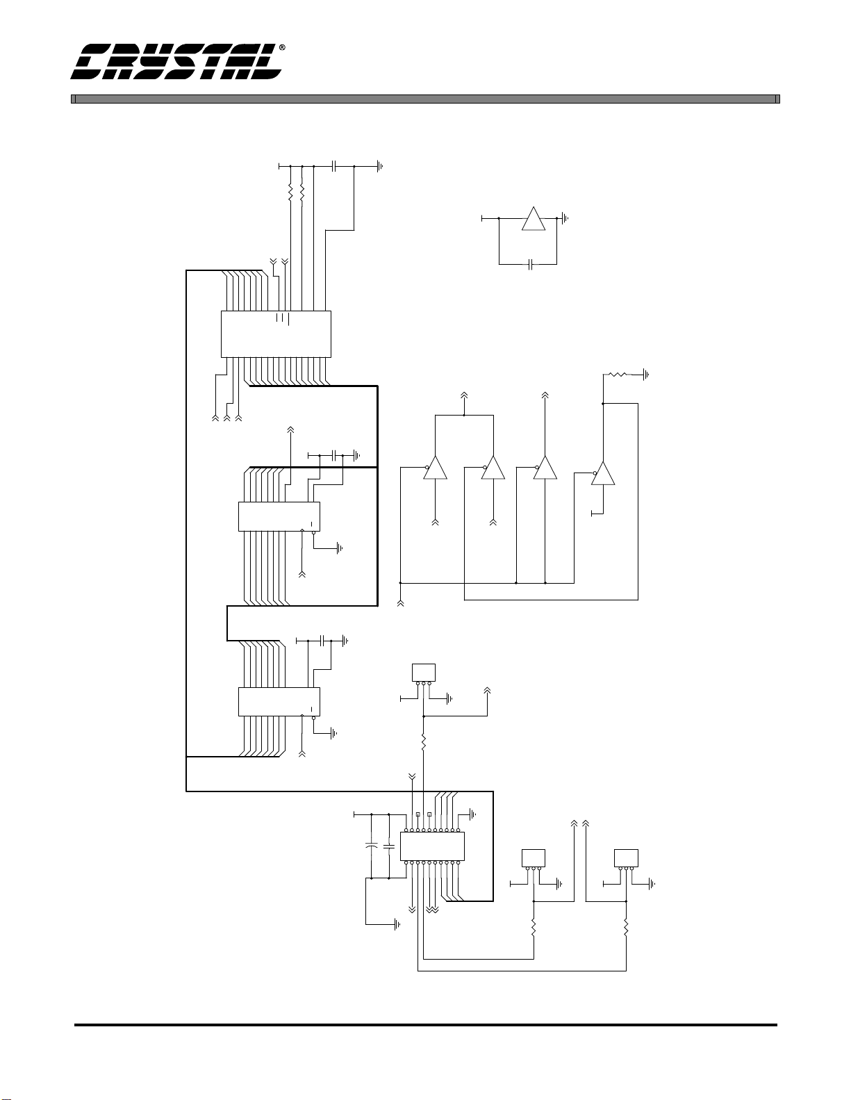
Digital Input
Control
Interface
RESET
CS8404A CS8404A CS8404A
CS8414
PLL
Digital Output
CRD4923-MEM
CDB49300-MEM
PLD
OSC
Figure 1. External Memory Example
input ports of the DSP. These configuration allows
the user to drive signals on stake headers J11 and
J12 in order to operate the DSP as if it were part of
an embedded system. The user is responsible for
providing the appropriate clocking signals, control
signals, and data signals to the DSP in full e xterna l
mode, but the user only provides control signals in
exernal control mode.
In the external modes the audio output of the DSP
still drives the on-board DACs and digital transmitters thus allowing the user to access the audio on
the analog and digital output connectors provided
by the CDB4923/300. The stake headers J11 and
J12 can be found in Figure 4.
All on-board clocks and data lines are routed
through the PLD (U11) in order to provide maximum flexibility in the evaluation of different system configurations. The PLD will perform all +5 V
to +3.3 V/+2.5 V conversions between the DSP
and the +5 V parts with which it interacts by configuring the I/O power jumper (J63). The system
can also be configured in an external interface described above. The external modes are detailed in
Data Selection. All PLD modes are selected using
CS4340
+2.5V
+3.3V
CS492x
CS493xx
CS4340
CS4340
CS5334
Patch Area
Analog
Output
Stereo
Analog In
DIP switch S3. The PLD (U11) and switch S3 are
shown in Figure 7.
A specialized IC (U12), the MAX708, has been included on the CDB4923/300 in order to generate a
system reset at power-up, when the digital power
begins to fail, and when the system reset button
(SW1) is depressed. This chip helps to insure consistent operation on the board by providing a
200 ms reset pulse whenever activated.
5. DATA SELECTION
Data selection on the CDB4923/300 refers to the
routing of audio data, audio clocks, control data,
and control clocks. Because the PLD plays such a
crucial role in determining the routing and control
scheme, each data selection mode is also referred to
as a ‘PLD mode.’ It is important to note that Table
2, the PLD Mode table, is based directly upon the
version of the control PLD (U11) used on each particular board. Each PLD has a specific revision
code printed on its label. If your PLD version differs from the one described in this document, contact the factory to determine which feature set is
provided with your board.
DS262DB2 9
Page 10

CDB4923 CDB49300
The two major PLD modes for the CDB4923/300
are the PROVIDED resource mode and the EXTERNAL interface mode. When a PROVIDED
mode is chosen all clocks are provided by the demonstration board, all audio data passes through the
PLD, and the DSP is controlled by the PC parallel
port interface. The EXTERNAL interface modes
allow the user to drive the audio data and control
pins of the DSP directly by wire-wrapping to stake
headers J11 and J12, bypassing the control PLD. It
should be noted that there are two variants of the
EXTERNAL interface mode. One EXTERNAL
mode provides direct access to all control and audio
data input pins of the CS492x/CS493xx, and the
second EXTERNAL mode allows the user to drive
the control signals of the CS492x/CS493xx while
audio data still comes from the CDB4923/300.
The DIP switch S3 is used to choose the different
routing schemes, and can be found in the Control
schematic of Figure 7. Table 2 provides a general
overview of the available PLD modes.
5.1 Provided Mode
When the user has chosen a PROVIDED resource
mode, the PLD Mode determines the source of audio data for the two data pins of the DSP (CMPDAT—pin 27 and SDATAN1—pin 22) and the
source of the system's oversampling clock
(MCLK). Table 3 lists the routing configurations
for each of the PROVIDED data selection modes.
5.1.1 Control
As mentioned earlier, when a PROVIDED mode
has been selected, all control of the CDB4923/300
is accomplished using the parallel port (J29). A
floppy disk is included with the CDB4923/300
which contains the control software described in
Appendix F: Board Control Software.
5.1.2 Data
All of the Data Selection Modes shown in Table 3
imply PC control. In Table 4, a brief description is
given for each data source listed in Table 3.
The general data flow of the system is illustrated in
Figure 2. A data path is shown for each of the
modes listed in Table 3.
PLD Mode DATA_SEL2 DATA_SEL1 DATA_SEL0 AUDIO DATA, CONTROL,
and CLOCKS
0 LO LO LO EXTERNAL J11
1 LO LO HI EXTERNAL CONTROL
ONLY
2 LO HI LO PROVIDED PC
3 LO HI HI PROVIDED PC
4 HI LO LO PROVIDED PC
5 HI LO HI PROVIDED PC
6 HI HI LO RESERVED
7 HI HI HI RESERVED
NOTE: Because each mode of the Data Selection switch (S3) sets up a different hardware configuration, clock
and data lines may be momentarily directed to many different destinations during mode changes. Without
the proper initiali za tio n pr o ces s aft er a r ec on figuration, strange beha vi or ma y b e o bse r ved . T he re co mmended procedure for pe rfor min g ch ang es to the r outi ng conf igu ratio n is to fir s t gen erate a bo ar d re se t
using the BOARD RESET switch (SW1). The CS492x/CS493xx will then require a soft reset
("CDB30RST.EXE -s" which performs a hardware reset and then sends the soft reset message
0x000001) and the proper hardware and applic ation co nfigurati on mess ages for the new mo de. A thorough description of soft reset, hardware configuration, and application configuration can be found in the
software Application Notes AN115, AN120-123, AN140 or AN161-163.
CONTROL SOURCE
J11
Table 2. Data Selection Modes (PLD version AB-X)
10 DS262DB2
Page 11

CDB4923 CDB49300
CS4340
XMT958
CS8414
CS8414
Data
CS8404A CS8404ACS8404A
CDI
DAI
Parallel Compressed Data
XMT958
CS492x
CS493x
x
Stereo PCM
CS4340
CS4340
PCM Out
CS5334
Figure 2. CDB4923/300 Data Paths
PLD
Mode
DATA_SEL2 DATA_SEL1 DATA_SEL0 CS492x/CS493xx
CMPDAT
CS492x/CS493xx
SDATAN1
2LO HI LO PC A/D — CS5334 DSP
3LO HI HIS/PDIF — CS8414 S/PDIF — CS8414 CS8414
4HI LO LOS/PDIF — C S8414 A/D — CS5334 CS8414
5HI LO HI A/D — CS5334 A/D — CS5334 OSC/PLL
MCLK
SOURCE
Table 3. PROVIDED Data Selection Modes (PLD version AB-X)
Digital Audio Source Description
S/PDIF - CS8414 The CS8414 (U13) delivers the payload from an IEC60958 (linear PCM) or IEC61937 (nonlinear
PCM) encoded bit-stream. The incoming S/PDIF stream is connected to either J32 or J30.
A/D - CS5334 The CS5334 (U25) delivers stereo PCM which has been enc oded from t he analog i nput signals on
J55 and J56.
PC A compressed digital audio stream is delivered in bursty format to the parallel port of the
CS492x/CS493xx from a fi le on the PC . Thi s tran sfe r mode requires that the CD B492 3/3 00 is in a
parallel communication mode, and the PARLLPLY.EXE program is then used to deliver compressed data through the PC interface.
NOTE: This data source is valid only for compressed audio and can be used only with parallel
communication modes (i.e. INTEL or Motorola mode).
Table 4. Digital Audio Sources
DS262DB2 11
Page 12

CDB4923 CDB49300
MCLK
Source
Description
CS8414 The CS8414 (U13) derives the sampling fre-
quency (Fs) from an incoming S/PDIF stream
and masters a 256 Fs MCLK
DSP The DSP (U1) masters MCLK, general ly when
using broadcast application code
OSC/PLL The source of the main DSP clock also sup-
plies the system 256 Fs MCLK (see Clocking
for details)
Table 5. Clocking Descriptions
5.1.3 Audio Clocking
The audio clocking scheme is illustrated below in
Figure 3. Note that MCLK is bidirectional with respect to the DSP. When the DSP is slaved to an external MCLK, i.e. the MCLK source is not listed a s
DSP, the DSP will slave to the MCLK of the
CS8414 or the MCLK derived from the on-board
PLL (U26) or the OSCILLATOR (Y1). When the
internal PLL of the CS492x/CS493xx is being
used, however, the DSP will master the MCLK.
Caution must be observed when choosing a particular data selection mode and configuring the DSP
to ensure that there is no contention with the PLD
(U11). Each PLD mode given in Table 3 lists the
associated MCLK master - this table should be referenced whenever reconfiguring the
CDB4923/300. A brief description of each MCLK
source is given in Table 5.
5.2 External Mode
The EXTERNAL mode is designed to allow users
to drive the DSP directly with an external microcontroller. Stake headers J11 and J12 contain all of
the signals required for host communication with
the CS492x/CS493xx. When operating in this
mode the DSP control pins are tri-stated by the
PLD (U11), effectively disabling the PC interface.
Consequently, the software bundled with the demo
board will not be functional.
The main DSP clock is always provided by the
CDB4923/300 (please see the Clocking section to
determine how to select the oscillator or external
PLL), and the output signals AUDATA0-2 are still
routed to the CS8404A S/PDIF transmitters and
CS4340 DACs.
Depending on the EXTERNAL mode selected the
user may be responsible for all data, control, and
clock signals going to the DSP, or just control.
CS8404A
CS8414 MCLK
CS8414
12 DS262DB2
OSC
PLL
NOTE: ALL SIGNALS DRIVEN TO THE CS493xx
CS8404A CS8404A
DIGITAL MCLK / ANALOG MCLK
DSP MCLK
DSP SCLK
DSP LRCLK
DIGITAL SCLK / ANALOG SCLK
DIGITAL LRCLK / ANALOG LRCLK
Figure 3. Audio Clocking
MUST BE +3.3 V LOGIC. Because the
CS493xx does not have +5 V tolerant pads, an
external buffer such a s the 74VHC244 should
be used for level conversion of any signals driven to the DSP. Failure to buffer +5 V signals
can cause permanent damage to the DSP. If
necessary, level shifting buffers can be wired
into the digital patch area of the CDB49300.
CS4340
CS4340
CS4340
CS492x
CS493xx
CS5334
Page 13

CDB4923 CDB49300
As mentioned above, many of the PLD’s I/O pins
are tri-stated. The complete list of tri-stated pins
for full external mode (PLD Mode 0) can be found
in Table 6. The complete list of tri-stated pins for
external control mode (PLD Mode 1) can be found
in Table 7.
By design, the clocking signals present at the
MCLK, LRCLK, and SCLK pins of the
CS492x/CS493xx are used to drive both the audio
input and output circuitry for the rest of the
CDB4923/300 as shown in Figure 3. This means
that the S/PDIF input, S/PDIF output, analog output and analog input continue to function in the
EXTERNAL modes. The user should only drive
audio clocks in PLD Mode 0. PLD Mode 1 derives
audio clocks from the CS8414.
The three clocking configurations that the user
should be aware of when using PLD Mode 0 are:
• DSP is slave to all audio clocks - user drives
MCLK/SCLK/LRCLK
• DSP masters LRCLK/SCLK - user drives
MCLK
Pin Name Pin
Number
RESET
RD
WR
A1, CDIN 6
A0, SCCLK 7
SCPDIO 19
CS
Table 7. DSP Pins Tri-Stated by U11 in PLD Mode 1
36
5
4
18
Pin Name Pin
Number
DATA0 17
DATA1 16
DATA2 15
DATA3 14
DATA4 11
DATA5 10
DATA6 9
DATA7 8
MCLK
Source
J12 The user must provide an oversampling clo ck on
the 23MCLK pin of stake header J12. (NOTE:
This clock signal must be +3.3 V logic when
using CS493xx)
CS8414 The CS8414 (U13) derives the sampling fre-
quency (Fs) from an incoming S/PDIF stream
and masters a 256 Fs MCLK
DSP The DSP (U1) masters MCLK, generally when
using broadcast application code
Description
• DSP masters MCLK/LRCLK/SCLK - user
drives no audio clocks
Pin Name Pin
Number
MCLK 44 DATA0 17
CMPCLK 28 DATA1 16
CMPREQ 29 DATA2 15
CMPDAT 27 DATA3 14
SCLKN1 25 DATA4 11
SLRCLKN1 26 DATA5 10
SDATAN1 22 DATA6 9
RESET
RD 5 A1, CDIN 6
WR 4 A0, SCCLK 7
EXTMEM 21 SCPDIO 19
Table 6. DSP Pins Tri-Stated by U11 in PLD Mode 0
36 DATA7 8
Pin Name Pin
CS
Number
18
Table 8. Clocking Descriptions
Only when the correct clocking is present on the
23MCLK, 23LRCLK, and 23SCLK pins (J12),
processed audio can be heard on the analog outputs
(J13 - J20) and the digital outputs (J45 - J47). The
analog outputs J13-J20 can be found in Figure 12,
and the digital outputs can be found in Figure 13.
The information in Table 9 summarizes the operation of switch S3. The table shows the data routing
configuration, the MCLK source, and the method
of board control. This is intended as a quick refer ence and can also be found in Appendix J: Switch
Summary.
DS262DB2 13
Page 14

CDB4923 CDB49300
6. CLOCKING
There are four major clocks routed across the
CDB4923/300: CLKIN for the DSP, MCLK, LRCLK, and SCLK. CLKIN is only used to drive the
digital logic of the DSP core. MCLK, LRCLK, and
SCLK are used for synchronizing the audio systems of the CDB4923/300.
6.1 DSP Clock
The DSP clock of the CS492x/CS493xx is provided at the CLKIN pin (pin 30). The setting of jumper
J1 (DSP CLOCK) determines whether the
CS492x/CS493xx uses the input clock as the DSP
clock directly (CLKIN position) or uses the input
clock as a reference for the internal PLL ( PLL position).
There are two possible clock sources on the
CDB4923/300. The first is the OSCILLATOR
(Y1). The second option is the external PLL (U26)
which can be configured to provide a processor
clock ranging from 33 MHz to 81 MHz. All clocking circuitry can be found in Figure 8.
Since the PLL (U26) and the OSCILLATOR (Y1)
are co-dependent, only one can be used at any given time. Jumper J37 is used to select the source of
the main DSP clock. It is vital to note that the jumper J37 is a double jumper with two jumpers which
must be moved in unison. If the jumpers are not
moved together, board behavior will be unpredictable. Table 11 lists the oscillator requirements, and
the two different settings for J37, where pins 3 and
4 are connected to the inputs of the PLD. Jumper
J37 can also be found in Figure 8.
In order to use the 27 MHz oscillator directly, Y1
should be populated with the 27 MHz oscillator included with the CDB4923/300 package. Addition-
Clock
Source
Oscillator 27 MHz or
External
PLL
Table 11. Board Clocking Configurat ions (J37)
Y1 J37 - Pin 3 J37 - Pin 4
OSC OSC
12.288 MHz
oscillator
27 MHz
oscillator
PLL PLL
PLD
Mode
0 LO LO LO Data and Control lines accessed via J11 and J12 J12 or DSP J11 & J12
1 LO LO HI S/PDIF -- CS8414 A/D -- CS5334 CS8414 J11 & J12
2 LO HI LO PC A/D -- CS5334 DSP PC
3 LO HI HI S/PDIF -- CS8414 S/PDIF -- CS8414 CS8414 PC
4 HI LO LO S/PDIF -- CS8414 A/D -- CS5334 CS8414 PC
5 HI LO HI A/D -- CS5334 A/D -- CS5334 OSC/PLL PC
6 HI HI LO RESERVED
7 HI HI HI RESERVED
PLD
Mode
0 LO LO LO J12 J12 J12 or DSP
1HIHIHIS/PDIF — CS8414 A/D -- CS5334 CS8414
14 DS262DB2
DATA
SEL2
DATA_SEL2 DATA_SEL1 DATA_SEL0 CS492x/CS493xx
DATA
SEL1
DATA
SEL0
Table 9. Data Selection Modes (Switch S3, PLD Version AB-X)
Table 10. EXTERNAL Data Selection Modes (PLD Version AB-X)
CS492X/CS493XX
CMPDAT
CS492X/CS493XX
SDATAN1
CMPDAT
MCLK
MASTER
CS492x/CS493xx
SDATAN1
CONTROL
SOURCE
MCLK
SOURCE
Page 15

CDB4923 CDB49300
ally, both jumpers of J37 should be set to the OSC
position. In this clocking configuration you should
not use any modes which list OSC/PLL as the
MCLK source while Y1 is 27 MHz.
In order to use the 12.288 MHz oscillator directly,
Y1 should be populated with the 12.288 MHz oscillator included with the CDB4923/300 package,
and both jumpers of J37 should be set to the OSC
position. The 12.288 MHz oscillator can be used
with those PLD modes naming OSC/PLL as the
MCLK source, as 12.288 MHz is a standard 256Fs
oversampling frequency (256 * 48 kHz).
The choice of 12.288 MHz or 27 MHz is application code dependent. Applications dealing with
IEC61937 packed compressed audio generally require a 12.288 MHz input, while broadcast applications typically require a 27 MHz input. Check the
relevant application code user’s guide (AN120AN123, AN140 or AN161-AN163) for details on
DSP CLKIN frequency.
If the external PLL is to be used, then Y1 must be
populated with a 27 MHz oscillator. The jumpers
of J37 should both be placed in the PLL position.
The CLKIN pin of the DSP will now be driven with
the processor clock (PCLK) output of U26. The
processor clock (PCLK) output can be configured
to generate either a many different frequencies,
based upon the configuration of jumpers J67, J68,
and J72 as listed in Table 12.
When using the external PLL to generate the DSP
clock, the CLKSEL pin (J1) of the
CS492x/CS493xx is typically set to ‘EXT CLK’.
6.2 MCLK
modes can select between an MCLK which is simply the frequency of the on-board oscillator (Y1),
or a programmable MCLK generated by the external PLL (U26).
The source of MCLK is dependent upon the PLD
mode and is indicated by the ‘MCLK SOURCE’
column of Table 9 and Table 24.
U26 is a discrete PLL which can generate many
different audio frequencies in addition to the processor clock discussed above. The frequency of the
audio clock is controlled by the states of the AS1
and AS0 pins which are set with jumpers J70 and
J71. The available audio clock frequencies can be
used to support many different sampling frequencies, depending on the desired MCLK ratio. Table
13 enumerates all possible MCLK frequencies for
the external PLL.
6.3 LRCLK and SCLK
LRCLK and SCLK are assumed to be generated by
the DSP in all cases. The audio clocking diagram
shown in Figure 3, illustrates the clocking scheme
of the CDB4923/300. If it is necessary to provide a
complete slave mode for the DSP, please contact
the factory for details on how to properly configure
the CDB4923/300.
PCLK Frequency J72 J67 J 68
33.33 MHz LOLOLO
54 MHz LO LO HI
66.66 MHz LO HI LO
80 MHz LO HI HI
32 MHz HI LO LO
81 MHz HI LO HI
50 MHz HI HI LO
40 MHz HIHIHI
The system MCLK on the CDB4923/300 can come
Table 12. PCLK Configurations
from four different sources when using a PROVIDED mode. Some PLD modes use the MCLK generated by the CS8414 S/PDIF receiver (U13) when
there is an incoming S/PDIF stream. In PLD mode
2, the DSP generates MCLK when it is decoding a
compressed bit stream delivered by the PC. Some
DS262DB2 15
MCLK Frequency AS1 (J70) AS0 (J71)
24.576 MH z 1 1
12.288 MH z 0 0
11 .28 96 MH z 0 1
8.192 MHz 1 0
Table 13. Audio Frequency Selection (J58)
Page 16

CDB4923 CDB49300
34DIF1 34DIF0 Digital Input Format
LO LO 20-Bit Lef t Justified, Rising SCLK
LO HI 20-Bit Left Justified, Falling SCLK
HI LO
20 Bit I
2
S, Rising SCLK (default)
HI HI Power Down
Table 14. CS5334 Digital Output Formats (S4)
7. INPUT
PARLLPLY.EXE program found on the included
floppy. Audio delivered across the S/PDIF inter-
7.1 Analog Input
A stereo input is provided at RCA jacks J55 and
J56. These inputs are designed to accept a full-scale
signal of 2 V
verted to a differential 2 V
applied to the inputs of the CS5334 ADC. The
CS5334 and its analog input buffers can be found
in Figure 9.
The CS5334’s clock signals can be accessed at the
test points labeled ALG_MCLK, ALG_SCLK, and
ALG_LRCLK (these test points can be found in
Figure 11). The serial data stream coming from the
CS5334 can be probed at the 34SDATA test point
(TP22). Jumper J52 is used to configure the
CS5334 for slave or master mode. The default,
slave mode, is used when the CS5334 accepts all
clock signals from another source. When in master
mode, the CS5334 accepts MCLK and generates
. Each single-ended signal is con-
rms
signal before being
rms
face comes from a digital source such as a DVD
player.
The S/PDIF inputs are J30 (RCA) and J32 (Optical), and can be found in Figure 10. It is vital to
note, though, that only one of these S/PDIF inputs
can be used at any given time . The active jack is determined by the setting of jumper J31 (S/P DIF IN).
When J31 is in the ’OPT’ position, S/PDIF data will
be accepted only from J32. When J31 is in the
’RCA’ position, S/PDIF data will be accepted only
from J30.
The S/PDIF signal is routed to the CS8414 receiver
(U13). The digital output format of the CS8414 is
configured using switch S1 as described in Table
15. The CDB4923/300 comes from the factory configured to operate in I2S mode. Note that this default should not be changed unless the DSP has
been configured to use a different serial format.
SCLK and LRCLK. The CDB4923/300 is configured to use the CS5334 in slave mode only. Please
contact the factory for details on how to use the
CS5334 in master mode.
The digital output format of the CS5334 can be
configured with switch S4 as described in Table 14.
More details on the CS5334 can be found in the
CS5334 datasheet.
7.2 Digital Input
There are two possible sources of digital audio for
the CDB4923/300: S/PDIF, and bursty delivery
from the host PC across the parallel interface.
Bursty delivery is accomplished by spooling a file
from the host PC to the CDB4923/300 using the
Jumpers J65 and J66 control the SEL and
CS12/FCK pins of the CS8414. These pins can be
used to select what is displayed on the channel status outputs of the Digital Audio Interface Receiver.
By default these pins are pulled up and the jum pers
are not stuffed. If the user wishes to change the values of these pins a stake header should be installed.
The CS8414, its control switch, and jumpers can be
found in Figure 10. If more details on the CS8414
are needed, please reference the CS8414 datasheet.
M2 M1 M0 Audio Serial Port Format
LO LO LO Out, L/R, 16-24 Bits
LO LO HI In, L/R, 16-24 Bits
LO HI LO
LO HI HI
HI LO LO Out, WSYNC, 16-24 Bits
HI LO HI Out, L/R, 16 Bits LSBJ
HI HI LO Out, L/R, 18 Bits LSBJ
HI HI HI Out, L/R, MSB Last
Out, L/R, I
In, L/R, I2S (default)
2
S
16 DS262DB2
Table 15. Digital Output Format settings
for CS8414 (S1)
Page 17
CDB4923 CDB49300
8. OUTPUT
8.1 Analog Output
The six discrete outputs provided on the
CDB4923/300 are driven by CS4340 D/A converters. They can be found at RCA jacks J13-J16, J18,
and J20. Each output is driven directly by the
CS4340 to provide a 3.5 Vpp full scale output. The
CS4340 and its control signals can be found in Figure 11, and the analog output buffers can be found
in Figure 12.
The digital input format of the CS4340 is configured using switch S4. The CDB4923/300 is
shipped with the CS4340 in I2S mode, and should
not be changed unless the CS492x/CS493xx has
been configured to use a different serial format.
The list of data formats for the CS4340 can be
found in Table 16. For more details on the features
of the CS4340, please reference the CS4340
datasheet.
down, and during audio clock discontinuities if the
reset period is violated.
8.3 Digital Output
The signals present on analog outputs J13-J16, J18,
and J20 can also be found on the digital outputs
J45-J47 (AOUTDIG0-AOUTDIG2). The optical
transmitters are driven by CS8404A S/PDIF transmitters (U19-21). The CS8404As are configured to
operate in consumer mode by default. The mode of
operation and status bits can be controlled by installing a 16 pin header in J44 and placing jumpers
on the signals that are to be programmed low. All
signals on J44 are pulled up by default. The
CS8404A transmitters and optical outputs can be
found in Figure 13.
The digital input format of the S/PDIF transmitt ers
can be controlled with switch S2 as listed in
Table 17. More operational details for the
CS8404A can be found in the CS8404A datasheet.
8.2 Analog Output Protection Circuitry
The CS4340 is designed to perform a ‘soft’ ramping of the bias voltage in order to prevent popping
on the outputs. However, the series capacitance
found in the analog buffers of the CS4340 require a
finite amount of time to discharge when the
CS4340 goes into reset (RC time constant). If the
full reset period is not observed before new audio is
delivered, popping can occur on the outputs. Please
see the CS4340 datasheet for more details.
The four transistors connected to the mute output of
each CS4340 are used to ensure that no 'popping'
will occur on the outputs during power-up, power-
27DIF1 27DIF0 Digital Input Format
LO LO
LO HI 16-24 Bit Left Justified
HI LO 24-Bit Right Justified
HI HI 16-Bit Right Justified
Table 16. CS4340 Digital Input Formats (S4)
16-24 Bit I2S (default)
Optical transmitter J43 (XMT958) is directly connected to the S/PDIF transmit ter of the DSP. It can
be used to directly observe the digital output of the
CS492x/CS493xx when the application code running on the part utilizes the transmitter. Note that if
the application code does not support S/PDIF transmission, J43 will not generate valid data. Please see
the application note associated with the code in
question (e.g. AN120-123, AN140, or AN161AN163) to determine whether J43 should be active.
M2 M1 M0 Audio Serial Port Format
LO LO LO FSYNC & SCK Output
LO LO HI Left/Right, 16-24 Bits
LO HI LO Word Sync, 16-24 Bits
LO HI HI Reserved
HI LO LO
HI LO HI LSB Justified, 16 Bits
HI HI LO LSB Justified, 18 Bits
HI HI 1 MSB Last, 16-24 Bits
Table 17. Digital Input Format settings
Left/Right, I
for CS8404A (S2)
2
S (default)
DS262DB2 17
Page 18

9. APPENDIX A: SCHEMATICS
CDB4923 CDB49300
Figure 4. CS492x/CS493xx
18 DS262DB2
Page 19

CDB4923 CDB49300
Figure 5. System Power
DS262DB2 19
Page 20

CDB4923 CDB49300
Figure 6. PC Interface
20 DS262DB2
Page 21

CDB4923 CDB49300
Figure 7. Control Logic
DS262DB2 21
Page 22

CDB4923 CDB49300
Figure 8. Clocking
22 DS262DB2
Page 23

CDB4923 CDB49300
Figure 9. Analog Input
DS262DB2 23
Page 24
CDB4923 CDB49300
Figure 10. Digital Input
24 DS262DB2
Page 25

CDB4923 CDB49300
Figure 11. D/A Converters
DS262DB2 25
Page 26

CDB4923 CDB49300
Figure 12. Analog Output
26 DS262DB2
Page 27
CDB4923 CDB49300
Figure 13. Digital Output
DS262DB2 27
Page 28

CDB4923 CDB49300
Figure 14. Top Layer
28 DS262DB2
Page 29

CDB4923 CDB49300
Figure 15. Bottom Layer
DS262DB2 29
Page 30

CDB4923 CDB49300
Figure 16. SSTOP
30 DS262DB2
Page 31
CDB4923 CDB49300
Figure 17. ASYSTOP
DS262DB2 31
Page 32

CDB4923 CDB49300
Figure 18. Layer 2
32 DS262DB2
Page 33

CDB4923 CDB49300
Figure 19. Layer 3
DS262DB2 33
Page 34

34 DS262DB2
10. APPENDIX D: BILL OF MATERIALS
Item Quan Reference Part Number Manufacturer Descriptio n
1 15 C1,C7,C8,C9,C91,C96,C101,C129,C132,C15
9,C160,C163,C164,C167,C168
2 42 C4,C10,C11,C12,C66,C67,C68,C69,C71,C72,
C90,C95,C100,C106,C107,C108,C109,C110,
C111,C112,C130,C133,C138,C139,C141,C14
3,C149,C150,C151,C152,C153,C157,C161,C
162,C165,C166,C169,C170,C172,C174,C175,
C176
3 6 C18,C24,C28,C36,C41,C48 T491B335K020AS KEMET CAP, 3.3UF, TANT, 3528, 20V, 10%
4 12 C19,C20,C25,C26,C29,C30,C37,C38,C42,C4
3,C49,C50
5 3 C51,C55,C148 T491D476M020AS KEMET CAP, 47UF, TANT, 7343, 20V, 20%
6 5 C56,C156,C158,C171,C173 T491C476M010AS KEMET CAP, 47UF, TANT, 6032, 20V, 20%
7 1 C57 C1206C474K3RAC KEMET CAP, .47UF, X7R, 1206, 25V, 10%
8 8 C58,C59,C60,C61,C62,C63,C64,C65 C1206C224K5RAC KEMET CAP, .22UF, X7R, 1206, 50V, 10%
9 3 C73,C75,C76 C1206C103K5RAC KEMET CAP, .01UF, X7R, 1206, 50V, 10%
10 1 C74 12062R683K9BB2 PHILIPS CAP, .068UF, X7R, 1206, 50V, 10%
11 1 C113 1206CG471J9BB2 PHILIPS CAP, 470PF, COG, 1206, 50V, 5%
12 3 C119,C122,C134 T491C106K020AS KEMET CAP, 10UF, TANT, 6032, 20V, 10%
13 2 C128,C120 C1206C100J5GAC KEMET CAP, 10PF, COG, 1206, 50V, 5%
14 2 C131,C121 C1206C222J5GAC KEMET CAP, 2200PF, COG, 1206, 50V, 5%
15 2 C140,C142 C1206C470J5GAC KEMET CAP, 47PF, COG, 1206, 50V, 5%
16 1 C154 C340C225K5R5CA KEMET CAP, 2.2UF, X7R, C340, 50V, 10%
17 1 C155 C330C103K5R5CA KEMET CAP, .01UF, X7R, C330, 50V, 10%
18 5 D2,D3,D4,D5,D6 LN1351C-TR PANASONIC LED, GREEN, 3216
19 2 FB5,FB2 542-FB43-226 MOUSER INDUCTOR, FERRITE BEAD
20 13 J1,J2,J3,J31,J52,J62,J63,J67,J68,J69,J70,J71
,J72
21 2 J11,J12 TSW-110-07-G-D SAMTEC STAKE HEADER, 10X2, .1"CENTER, GOLD
22 1 J37 TSW-103-07-G-D SAMTEC STAKE HEADER, 3X2, .1" CENTER, GOLD
23 1 J44 TSW-108-07-G-D SAMTEC STAKE HEADER, 8X2, .1" CENTER, GOLD
24 4 J59,J60,J65,J66 TSW-102-07-G-S SAMTEC STAKE HEADER, 1X2, .1"CENTER, GOLD
25 1 J64 TSW-111-07-G-S SAMTEC STAKE HEADER, 11X1, .1"CENTER, GOLD
26 9 J13,J14,J15,J16,J18,J20,J30,J55,J56 16PJ097 MOUSER CONNECTOR, RCA, RA, GOLD
27 1 J21 111-0110-001 JOHNSON COMPONENTS BINDING POST, BLUE
28 2 J24,J22 111-0103-001 JOHNSON COMPONENTS BINDING POST, BLACK
29 1 J23 111-0102-001 JOHNSON COMPONENTS BINDING POST, RED
T491B105M035AS KEMET CAP, 1UF, TANT, 3528, 35V, 10%
C1206C104K5RAC KEMET CAP, .1UF, X7R, 1206, 50V, 10%
C1206C152F5GAC KEMET CAP, 1500PF, COG, 1206, 50V, 1%
TSW-103-07-G-S SAMTEC STAKE HEADER, 3X1, .1"CENTER, GOLD
CDB4923 CDB49300
Page 35

DS262DB2 35
Item Quan Reference Part Number Manufacturer Descriptio n
30 1 J57 111-0104-001 JOHNSON COMPONENTS BINDING POST, GREEN
31 1 J29 747238-4 AMP CONNECTOR, D-SUB, 25-PIN, MALE, RA
32 1 J32 TORX173 TOSHIBA OPTICAL TOSLINK RECIEVER
33 4 J43,J45,J46,J47 TOTX173 TOSHIBA OPTICAL TRANSMITTER
34 1 L1 43LS475 MILLLER INDUCTOR, 47UF
35 3 Q1,Q5,Q9 MMUN2111LT1 MOTOROLA TRANSISTOR, PNP, SOT-23
36 3 Q2,Q6,Q10 MMUN2211LT1 MOTOROLA TRANSISTOR, NPN, SOT-23
37 6 Q3,Q4,Q7,Q8,Q11,Q12 2SC2878 TOSHIBA TRANSISTOR , TO-92
38 2 RP5,RP1 4610X-101-103 BOURNS RES NETWORK, 10K-OHM, 10-PIN, BUSSED
39 1 RP2 4606X-101-102 BOURNS RES NETWORK, 1K-OHM, 6-PIN, BUSSED
40 1 RP3 4610X-101-102 BOURNS RES NETWORK, 1K-OHM, 10-PIN, BUSSED
41 1 RP4 4606X-101-103 BOURNS RES NETWORK, 10K-OHM, 6-PIN, BUSSED
42 37 R1,R2,R49,R54,R59,R66,R74,R80,R112,R120
,R150,R151,R152,R153,R160,R161,R163,R1
64,R184,R185,R186,R192,R193,R194,R212,
R214,R216,R222,R224,R233,R235,R242,R24
8,R249,R256,R257,R258
43 3 R6,R196,R197 CRCW1206472JT DALE RES, 4.7K-OHM,1206, 5%, 1/8W , METAL FILM
44 38 R14,R17,R19,R24,R26,R28,R31,R34,R36,R4
1,R87,R88,R89,R90,R91,R92,R94,R96,R98,R
100,R102,R103,R104,R105,R106,R107,R110,
R126,R129,R130,R131,R190,R191,R198,R20
0,R239,R240,R241
45 6 R50,R55,R60,R67,R75,R81 CRCW12065610FT DALE RES, 560-OHM, 1206, 1%, 1/4W, METAL FILM
46 3 R84,R85,R226 CRCW12061001FT DALE RES, 1K-OHM, 1206, 1%, 1/8W, METAL FILM
47 5 R86,R210,R217,R220,R229 CRCW1206151JT DALE RES, 150-OHM, 1206, 5%, 1/8W, METAL
48 5 R109,R119,R156,R169,R173 CRCW1206000ZP DALE RES, 0-OHM, 1206, 1%, 1/8W, METAL FILM
49 2 R114,R225 CRCW12062R0JT DALE RES, 2-OHM, 1206, 5%, 1/8W, METAL FILM
50 1 R117 CRCW12064750FT DALE RES, 470-OHM, 1206, 1%, 1/4W, METAL FILM
51 1 R118 CRCW1206750JT DALE RES, 75-OHM, 1206, 5%, 1/4W, METAL FILM
52 1 R155 CRCW12063320FT DALE RES, 330-OHM, 1206, 1%, 1/8W, METAL FILM
53 4 R175,R187,R188,R189 CRCW12061782FT DALE RES, 17.8K-OHM, 1206, 1%, 1/8W, METAL
54 4 R211,R221,R232,R247 CRCW12064752FT DALE RES, 47K-OHM, 1206, 1%, 1/8W, METAL FILM
55 2 R218,R228 CRCW1206203JT DALE RES, 20K-OHM, 1206, 5%, 1/8W, MET AL FILM
56 1 R246 CRCW12063302FT DALE RES, 33K-OHM, 1206, 1%, 1/8W, METAL FILM
57 6 R250,R251,R252,R253,R254,R255 CRCW1206202JT DALE RES, 2K-OHM, 1206, 5%, 1/4W, METAL FILM
58 1 R259 CRCW1206510JT DALE RES, 51-OHM, 1206, 5%, 1/4W, METAL FILM
CRCW12061002FT DALE RES, 10K-OHM, 1206, 1%, 1/8W, METAL FILM
CRCW1206330JT DALE RES, 33-OHM, 1206, 5%, 1/4W, METAL FILM
FILM
FILM
CDB4923 CDB49300
Page 36

36 DS262DB2
Item Quan Reference Part Number Manufacturer Descriptio n
59 1 SW1 PT645TL50 C&K SWITCH,PB,DPST,5 LEG
60 3 S1,S2,S3 76SB03 GRAYHILL DIP SWITCH, 3 POSITION
61 1 S4 76SB04 GRAYHILL DIP SWITCH, 4 POSITION
62 14 TP5,TP17,TP18,TP19,TP20,TP21,TP22,TP23
,TP24,TP25,TP26,TP27,TP28,TP29
63 1 U1 CS493001-CL CRYSTAL
64 1 UX1 540-93-044-24-000 MILL-MAX SOCKET-D.U.T. HOLE, PLCC-44, PIH
65 1 U8 LM3940IT-3.3 NATIONAL
66 2 U10,U9 DM74ALS541WM FAIRCHILD
67 1 U11 EPM7128ALC84-12 ALTERA INTEGRATED CIRCUIT, PLCC84
68 1 UX11 540-99-084-24-000 MILL-MAX SOCKET, PLCC-84, PIH
69 1 U12 MAX708ACT MAXIM INTEGRATED CIRCUIT, SUPERVISORY
70 1 U13 CS8414-CS CRYSTAL SEMI. INTEGRATED CIRCUIT, SOIC28 - WIDE
71 3 U16,U17,U18 CS4340-KS CRYSTAL INTEGRATED CIRCUIT, 24-bit, 96kHz DAC,
72 3 U19,U20,U21 CS8404A-CS CRYSTAL
73 2 U23,U24 MC33078-P MOTOROLA INTEGRATED CIRCUIT, DUAL OP AMP, DIP-8
74 2 UX23,UX24 110-93-308-41-001 MILL-MAX S0CKET, 300-MILL, DIP-8
75 1 U25 CS5334-KS CRYSTAL
76 1 U26 MK2744-10S MICRO-CLOCK INTEGRATED CIRCUIT,
77 1 U27 LM2937ET-2.5 NATIONAL
78 1 Y1 CX21AF-27.000MHZ CAL CRYSTAL OSCILATOR,, 27.000MHZ, TTL/CMOS, DIP-14
79 1 YX1 110-93-314-41-001 MILL-MAX S0CKET, 300-MILL, DIP-14
80 2 Z1,Z4 P6KE16A MOTOROLA DIODE, ZENER, AXIAL, 13V, DO-15
81 1 Z2 P6KE6.8A MOTOROLA DIODE, ZENER, AXIAL, 6.8V, DO-7
82 5 J21,J22,J23,J24,J57 L1.50x.25TX.25T,
83 2 FB5,FB2 C2015L-1000-ND DIGI-KEY 24AWG/HOOK-UP/STRNED FOR FERRITE
84 6 HARDWARE 8F1943 NEWARK STANDOFFS
85 6 HARDWARE HD343-ND DIGI-KEY SCREWS, 4/40, 1/4"
86 1 PCB CDB4923/30 REV-A PROTECH PRINTED CIRCUIT BOARD
TSW-101-07-G-S SAMTEC STAKE HEADER, 1X1, .1"CENTER, GOLD
+3.3V REGULATOR, TO-220
SEMICONDUCTOR
IC,OCTAL BUFFER/LINE DRIVER/LINE
SEMICONDUCTOR
SEMICONDUCTOR
SEMICONDUCTOR
SEMICONDUCTOR
SQUIRES BINDING POST HOOK UP WIRES
TY PE E 24/19
RECIEVER,SO20
CIRQUIT,
16pin SOIC
INTEGRATED CIRCUIT, SOIC24 - WIDE
INTEGRATED CIRCUIT, SSOP20
VOLTAGE REGULATOR, +2.5V, TO-220
BEADS
CDB4923 CDB49300
Page 37
11. APPENDIX E: EXTERNAL MEMORY SCHEMATICS
C3
.1uF
+3.3V
10k
10k
R14
D0D1D2D3D4D5D6
O013O114O215O317O418O519O620O7
EXTMEM
D7
22OE24
21
EMOE
CE
R13
+3.3V
31
32
1
16
VPP
VCC
GND
PGM
74LVC125
U5E
7 14
C5
.1uF
CDB4923 CDB49300
U3
A1730A162A153A1429A1328A124A1125A1023A0926A08
A14
A12
A13
uC17
uC16
A15
A8
A9
A10
19
D02D13D24D35D46D57D68D7
U2
A0A1A2A3A4A5A6
A0
A1A2A3A4A5A6A7
19
D02D13D24D35D46D57D68D7
U1
D0D1D2D3D4D5D6
A11
A11
A10
A12
A75A66A57A48A39A210A111A0
27
A8
A6
A7
A9
A14
A13
Q712Q613Q514Q415Q316Q217Q118Q0
9
A7
Q712Q613Q514Q415Q316Q217Q118Q0
9
D7
A5
A3
A4
DSP15
+3.3V
20
VCC
CK
11
EMOEEMOE
+3.3V
20
VCC
CK
11
AT27LV020A-90JC
12
A1
A2
A0
C2
.1uF
1
10
GND
OE
1
TC74VHC574FW
U5A
A[0:14]
C1
.1uF
10
GND
OE
1
TC74VHC574FW
uC17
uC16
+3.3V
123
A15
4
74LVC125
2 3
uC15
3X1HDR
0
U5B
5 6
DSP15
uC16
74LVC125
10
U5C
REQ23
74LVC125
9 8
13
U5D
+3.3V
10k
R1
74LVC125
12 11
Figure 20. CRD4923-MEM Schematic
R10
REQ23
D3D4
D5D6
+3.3V
47uF
C7
D7
+
.1uF
P1
C6
1 2
3 4
5 6
7 8
9 10
11 12
13 14
15 16
17 18
19 20
D0
D2 D1
EMOE
EXTMEM
MRESET23
uC15
+3.3V
123
uC15
uC17
3X1HDR
uC17
123
3X1HDR
+3.3V
0
R9
0
R8
DS262DB2 37
Page 38

38 DS262DB2
EMAD[7:0]
uC17
uC15
#EXTMEM #EMWR
#EMOE
49.9
R5
49.9
R7
49.9
R9
49.9
R3
EMAD[7:0]
U2
EMAD0
2
EMAD1
3
D1
EMAD2
4
D2
EMAD3
5
D3
EMAD4
6
D4
EMAD5
7
D5
EMAD6
8
D6
EMAD7
9
D7
11
VCC
GNDOE
74LVC574
#RESET
EMAD6
EMAD4
EMAD2 EMAD1
EMAD0
EMAD7
EMAD6
EMAD5
EMAD4
EMAD3
EMAD2
EMAD1
EMAD0
19
Q0CKD0
18
Q1
17
Q2
16
Q3
15
Q4
14
Q5
13
Q6
12
Q7
20
101
11 12
13 14
15 16
17 18
19 20
EMAD[7:0]
A0
A1
A2
A3
A4
A5
A6
A7
47uF
C6
+
0.1uF
C7
P1
1 2
3 4
5 6
7 8
9 10
R10
R11
R12
R13
R14
R15
R17
R18
A0
A1
A2
A3
A4
A5
A6 A14
A7
+3.3V
#EMOE#EMOE #EMOE
C1
0.1uF
+3.3V
EMAD7
EMAD5
EMAD3
49.9
49.9
49.9
49.9
49.9
49.9
49.9
49.9
R19
+3.3V
U3
A8
19
2
Q0CKD0
A9
18
3
Q1
D1
A10
17
4
Q2
D2
A11
16
5
Q3
D3
A12
15
6
Q4
D4
A13
14
7
Q5
D5
A14
13
8
Q6
D6
A15
12
9
Q7
D7
11
20
+3.3V
101
C2
0.1uF
#ABOOT
49.9
uC18
49.9
uC16
49.9
D7
2
A1
D6
3
A2
D5
4
A3
D4
5
A4
D3
6
A5
D2
7
A6
D1
8
A7
D0
9
A8
19
1G
1
DIR
74LVC574
18
17
16
15
14
13
12
11
20
10
VCC
GNDOE
R4
R6
R8
U7
Y1
Y2
Y3
Y4
Y5
Y6
Y7
Y8
VCC
GND
74VHC245
0
C9
0.1uF
A8
A9
A10
A11
A12
A13
A15
uC18
D[7:0]
#EXTMEM
#EMWR
U4
2
3
4
5
6
7
8
9
11
74LVC574
U1
30
A14
A13
A12
A11
A10
A9
A8
A7
A6
A5
A4
A3
A2
A1
A0
A16
A15
A14
A13
A12
A11
A10
A9
A8
A7
A6
A5
A4
A3
A2
A1
A0
+3.3V
2
3
29
28
4
25
23
26
27
5
6
7
8
9
10
11
12
A17
A16
A15
A14
A13
A12
A11
A10
A09
A08
A7
A6
A5
A4
A3
A2
A1
A0
AT27LV020A
U5
8
VCC
10
A16
7
A15
11
A14
A13
12
A12
1
A11
31
A10
2
A9
3
A8
13
A7
14
A6
15
A5
16
A4
17
A3
18
A2
19
A1
20
A0
CY7C109V33
uC17
uC16
A16
19
Q0CKD0
18
Q1
D1
17
Q2
D2
16
Q3
D3
15
Q4
D4
14
Q5
D5
13
Q6
D6
12
Q7
D7
20
VCC
GNDOE
+3.3V
101
C3
0.1uF
uC15
A[16:0]
U6A
1
2 3
#ABOOT
74LVC125
+3.3V
U6D
13
12 11
74LVC125
#uC18
R16
10K
+3.3V
C8
0.1uF
U6E
74LVC125
7 14
D0
13
O0
D1
14
O1
D2
15
O2
D3
17
O3
D4
18
O4
D5
19
O5
D6
20
O6
D7
21
O7
22
CE
24
OE
31
PGM
1
VPP
32
VCC
16
GND
+3.3V
C5
0.1uF
R2
10K
6
CE2
32
OE
30
CE1
54
WE
29
D7
28
D6
27
D5
26
D4
25
D3
23
D2
22
D1
21
D0
9
NC
24
GND
D[7:0]
R1
#EXTMEM
#uC18
#EMWR
D[7:0]
+3.3V
10K
C4
0.1uF
uC18
#EXTMEM
#EMWR
D0
D1
D2
D3
D4
D5
D6
D7
CDB4923 CDB49300
Figure 21. CDB49300-MEM Schematic
Page 39

12. APPENDIX F: BOARD CONTROL SOFTWARE
CDB4923 CDB49300
There is a suite of programs used to control the
CDB4923/300. The definitions given refer to
‘CDB30’ executables which should be used with
the both the CDB4923 and the CDB300.
These software tools are designed to operate from
a DOS prompt and can work with any parallel port
address (LPT1, LPT2, or LPT3). The default address for all of the programs is 0x378 (also known
as LPT1), but the port address can be changed by
using the '-p' option provided with every tool. Each
time a program is executed, the address that was
used is echoed to the screen. If a program seem
s to
fail, verification of the parall el port address should
the first step in troubleshooting.
All of these programs are designed to access the
CS492x/CS493xx using SPI or I2C serial communication, or INTEL or MOTOROLA parallel communication. The communication mode can be
chosen from the command line with the '-m' option.
It should be remembered that the mode chosen
must correspond to the communication mode used
by the CS492x/CS493xx. If the DSP is using a
communication mode which does not match the
software setting, results will be unpredictable.
Please see Digital Signal Processor of this
datasheet to learn how to change the DSP’s communication mode.
The source code for all programs can be found on
the floppy disk provided with the CDB4923/300.
These programs are documented and will provide
insight into communicating successfully with the
CS492x/CS493xx. The source for CDB30_LD is
particularly useful since it demonstrates the full
handshaking protocol required during boot-up of
the CS492x/CS493xx.
CDB30_LD - program used to load code into the CS492x/CS493xx.
Usage: cdb30_ld <input_file.ld> [-pXXX] [-mY] [-v]
-p = parallel port address
XXX = address (0x278, 378* or 3bc)
-m = communication mode
Y = mode designator (i = I2C*, s=SPI, m=MOT, n=INT)
-v = disable verbose mode
* = default
CDB30CMD - program used to send commands, or configuration files to the CS492x/CS493xx.
Usage: cdb30cmd <[ABCDEF] or [-fY]> [-mZ] [-pXXX] [-v]
ABCDEF = Three byte hex command
-f = send configuration file
Y = .cfg file with configuration parameters
-p = parallel port address
XXX = address (0x278, 378* or 3bc)
-m = communication mode
Z = mode designator (i = I2C*, s = SPI, m=MOT, n=INT)
-v = disable verbose mode
DS262DB2 39
Page 40

* = default
EXAMPLES:
cdb23cmd 000001 -p3bc
cdb23cmd -fac3.cfg -mS -p3bc
CDB4923 CDB49300
CDB30_RD - program used to read back responses from the CS492x/CS493xx. If the INTREQ
pin is not low when CDB30_RD is executed, the program will wait until INTREQ
drops. Press the ‘Enter’ key to exit the read wait loop.
Usage: cdb30_rd [-pXXX] [-mY] [-v] [-h]
-p = parallel port address
XXX = address (0x278, 378* or 3bc)
-m = communication mode
Y = mode designator (i = I2C*, s = SPI, m=MOT, n=INT)
-v = disable verbose mode
-h = this message
* = default
CDB30RST - program used to perform hard reset or soft reset on the CS492x/CS493xx.
Usage: cdb30rst [-s] [-pXXX] [-mY] [-v] [-h]
-s = Soft Reset
-p = parallel port address
XXX = address (0x278, 378* or 3bc)
-m = communication mode
Y = mode designator (i = I2C*, s = SPI, m=MOT, n=INT)
-v = disable verbose mode
-h = this message
* = default
PARLLPLY - program used to deliver compressed audio files to the parallel host port
of the CS492x/CS493xx from the PC.
Usage: parllply <input_file> [-pXXX] [-mY] [-l] [-b] [-cNNN]
-p = parallel port address
XXX = address (0x278, 378* or 3bc)
-l = Loop Mode
-b = Byte Swap
40 DS262DB2
Page 41

CDB4923 CDB49300
-m = Parallel control mode
Y = n (INTEL) or m (MOTOROLA)*
-c = Chunk Size
NNN = transfer size in words (252*)
* = default
CDB30_AD - program used to demonstrate autodetection on the CDB4923/300 only with
IEC61937 or IEC60958 input. This program will download new application code
from the PC each time a format change has been detected. The user should
specify ‘invalid’ for any application code or configuration file which does
not exist. This program only allows serial control.
Usage: cdb30_ad <AC3 .ld> <AC3 .cfg> <MPEG .ld> <MPEG .cfg> <DTS .ld> <DTS .cfg>
<PCM .ld> <PCM .cfg> [-pXXX] [-mY] [-v]
Specify invalid for non-existent .ld/.cfg.
-p = parallel port address
XXX = address (0x278, 378* or 3bc)
-m = communication mode
Y = mode designator (i = I2C*, s = SPI)
-v = disable verbose mode
* = default
EXAMPLE:
cdb30_ad ac3_263b.ld ac3_ad.cfg invalid invalid dts_2637.ld dts_ad.cfg
ac3_263b.ld pcm_ad.cfg -p3bc -ms
DS262DB2 41
Page 42

CDB4923 CDB49300
13. APPENDIX G: IC COMPONENT LISTING BY FUNCTION
13.1 POWER
U8 3.3 V Voltage Regulator {Figure 5}
U27 2.5 V Voltage Regulator {Figure 5}
13.2 RESET
U12 MAX708 Reset chip {Figure 7}
13.3 CLOCKING
U26 MK2744 Programmable Phase Locked Loop (PLL) {Figure 8}
Y1 Oscillator {Figure 8}
13.4 SIGNAL ROUTING/LEVEL CONVERSION
U11 EPM7128E Programmable Logic Device {Figure 7}
13.5 DSP
U1 CS492x/CS493xx Multi-Channel Audio Decoder {Figure 4}
13.6 INPUT
U9 Signal Buffer for Parallel Port {Figure 6}
U10 Signal Buffer for Parallel Port {Figure 6}
U13 CS8414 S/PDIF receiver {Figure 10}
U23 MC33078 Analog Input Buffer {Figure 9}
U24 MC33078 Analog Input Buffer {Figure 9}
U25 CS5334 20-bit A/D converter {Figure 9}
13.7 OUTPUT
U16 CS4340 20-bit D/A converter {Figure 11}
U17 CS4340 20-bit D/A converter {Figure 11}
U18 CS4340 20-bit D/A converter {Figure 11}
U19 CS8404A S/PDIF transmitter {Figure 13}
U20 CS8404A S/PDIF transmitter {Figure 13}
U21 CS8404A S/PDIF transmitter {Figure 13}
42 DS262DB2
Page 43

14. APPENDIX H: JUMPERS LISTED BY FUNCTION
14.1 AUDIO INPUT JUMPERS
J31 This jumper is used to select the input connector which is being used to receive S/PDIF data.
Placing the jumper in the ’RCA’ position enables the RCA jack, and placing the jumper in the
’OPT’ position enables the TORX173 optical receiver.
Default: OPT
J52 This jumper is used to control the MASTER/SLAVE clocking mode of the CS5334 as described
in the CS5334 datasheet. This jumper should be left in the ’SLAVE’ position when using the factory programmed PLD provided with the CDB4923/300.
Default: SLAVE
J65 This jumper is used to control the SEL pin of the CS8414. This pin, in conjunction with J66, is
used to select which channel status pin information to display on the status output pins. Please
refer to the CS8414 datasheet for more details on how to configure the CS8414.
Default: HI (Not Populated).
J66 This jumper is used to control the CS12/FCK pin of the CS8414. This pin, in conjunction with
J65, is used to select which channel status pin information to display on the status output pins.
Please refer to the CS8414 datasheet for more details on how to configure the CS8414.
Default: HI (Not Populated).
CDB4923 CDB49300
14.2 AUDIO OUTPUT JUMPERS
J44 This particular component is actually a set of jumpers. Each individual jumper can be used to
control the state of one channel status bit in the outgoing S/PDIF stream created by the
CS8404A. More details can be found in the datasheet for the CS8404A and the specifications
for IEC60958 and IEC61937 bitstreams.
Default: All bits HI {Not Populated}
14.3 DSP JUMPERS
J1 This jumper is used to control the internal clocking of the CS492x/CS493xx. When in the
’CLKIN’ position, the CS492x/CS493xx uses the clock on the CLKIN pin to drive the DSP core
directly. When in the ’PLL’ position, the CS492x/CS493xx derives all internal clocks from the
reference frequency provided at the CLKIN pin.
Default: CLKIN
J2 This jumper selects the pull-up/pull-down state of the CS492x/CS493xx’s WR
is used in conjunction with J3 and J62 to select the Host Interface Mode of the
CS492x/CS493xx when it comes out of reset. By default the CDB4923/300 is configured for I2C
serial communication. The settings for J2 (WR
CS4923/4/5/6/7/8/9 datasheet and the CS49300 datasheet.
Default: HI
J3 This jumper selects the pull-up/pull-down state of the CS492x/CS493xx’s RD
is used in conjunction with J2 and J62 to select the Host Interface Mode of the
CS492x/CS493xx when it comes out of reset. By default the CDB4923/300 is configured for I
serial communication. The settings for J2 (WR
CS4923/4/5/6/7/8/9 datasheet and the CS49300 datasheet.
Default: LO
pin. This jumper
), J3 (RD) and J62 (PSEL) are detailed in the
pin. This jumper
), J3 (RD) and J62 (PSEL) are detailed in the
2
C
J11 Stake header providing some serial communication lines, and all general purpose I/O pins. This
header is also serves as the memory interface to the CRD4923_MEM/CDB49300_MEM. This
DS262DB2 43
Page 44

header can be used to probe signals during normal operation, and may be used as a wirewrap
point when using Data Selection Mode 0 or 1, as detailed in the Data Selection section of this
datasheet.
J12 Stake header providing access to all serial audio data and clock pins. This header can be used
to probe signals during normal operation, and may be used as a wirewrap point when using
Data Selection Mode 0 or 1, as detailed in the Data Selection section of this datasheet
J62 This jumper selects the pull-up/pull-down state of the CS492x/CS493xx’s PSEL pin. When
coming out of reset, the state of the PSEL pin determines which parallel interface mode to use
(Motorola or Intel) when initializing the CS492x/CS493xx into a parallel host interface mode.
This jumper is used in conjunction with J2 and J3 to select the Host Interface Mode of the
CS492x/CS493xx when it comes out of reset. Because the PSEL pin has multiplexed functionality it also serves as SCDIO when in I
the board is initially configured for I
The settings for J2 (WR
datasheet and the CS49300 datasheet.
Default: HI
14.4 POWER JUMPERS
J59 This jumper connects DSP_PWR to the analog side of the CS492x/CS493xx. Analog current con-
sumption can be measured by removing this jumper and connecting an ammeter in series with the
jumper.
Default: INSTALLED
CDB4923 CDB49300
2
C mode. By default this jumper is in the ’HI’ position since
2
C serial communication and the SCDIO pin is open-drained.
), J3 (R D) and J62 (PSEL) are detailed in the CS4923/4/5/6/7/8/9
J60 This jumper connects DSP_PWR to the digital side of the CS492x/CS493xx. Digital current
consumption can be measured by removing this jumper and connecting an ammeter in series
with the jumper.
Default: INSTALLED
J63 This jumper is used to select the maximum voltage at which the I/O pins of the system PLD
(U11) will drive its outputs. The user can select between +3.3 V and +2.5 V.
Default: +3.3 V
J69 This jumper (DSP_PWR) is used to select the core voltage for DSP power. This jumper is pro-
vided to allow the user to evaluate both the CS4923/4/5/6/7/8 family and the CS49300 family of
audio decoders. The CS4923/4/5/6/7/8 family requires +3.3 V, while the CS49300 family requires +2.5 V. The user can select between +3.3 V and +2.5 V.
CDB4923 Default: +3.3 V
CDB49300 Default: +2.5 V
14.5 SYSTEM CLOCKING JUMPERS
J37 This dual position jumper select between an oscillator or the MK2744-10S discrete PLL (U26)
as the external clock source for the DSP of the CS492x/CS493xx, and it also selects the system
MCLK for non-S/PDIF input modes. It is important to note the jumpers of J37 must move together. They must be both in the ’OSC’ position or they must both be in the ’PLL’ position. Moving
only one jumper will result in erratic behavior.
When both jumpers are in the ’OSC’ position, the CS492x/CS493xx CLKIN pin is driven by the
oscillator, Y1, and some of the data modes chosen by switch S3 will provide a system MCLK
which is also derived from Y1. Specifically, all data selection modes listed in Table 9 and Table
24 showing an MCLK Source of ’OSC/PLL’ will generate a system MCLK equal to the frequency
of the oscillator Y1.
If you have questions about how to utilize the external PLL, please contact the factory before
44 DS262DB2
Page 45

CDB4923 CDB49300
adjusting this jumper. Y1 must be a 27 MHz oscillator before attempting to use U26. When
both jumpers are in the ’PLL’ position, U26 will drive the CLKIN pin of the CS492x/CS493xx with
the configured PCLK (refer to Table 12 or Table 22), and the system MCLK will be driven by
ACLK. The frequency of MCLK can be programmed by changing the values of the AS1 and AS0
pins of U26 as detailed in Table 13 of this datasheet.
Default: OSC OSC
J67 Jumper used to set the value of the PS1 pin of U26. This jumper, in conjunction with J68 and
J72, determines the processor clock frequency provided by the external PLL. Please refer to
Table 12 or Table 22 for more details.
Default: LO
J68 Jumper used to set the values of the PS0 pin of U26. This jumper, in conjunction with J67 and
J72, determines the processor clock frequency provided by the external PLL. Please refer to
Table 12 or Table 22 for more details.
Default: HI
J70 Jumper used to set the values of the AS1 pin of U26. This jumper, in conjunction with J71, de-
termines the MCLK frequency provided by the external PLL. Please refer to Table 13 for more
details.
Default: HI
J71 Jumper used to set the values of the AS0 pin of U26. This jumper, in conjunction with J70, de-
termines the MCLK frequency provided by the external PLL. Please refer to Table 13 for more
details.
Default: 50
J72 Jumper used to set the values of the PS2 pin of U26. This jumper, in conjunction with J67 and
J68, determines the processor clock frequency provided by the external PLL. Please refer to
Table 12 or Table 22 for more details.
Default: LO
DS262DB2 45
Page 46

15. APPENDIX I: JUMPERS LISTED BY NUMBER
NOTE: Each jumper listed below is described in Appendix H: Jumpers Listed by Function. The
relevant section heading is listed beside each jumper name in braces {}.
J1 CS492x/CS493xx DSP clock {DSP Jumpers}
Default: CLKIN
J2 CS492x/CS493xx WR
Default: HI
pin {DSP Jumpers}
CDB4923 CDB49300
J3 CS492x/CS493xx RD
Default: LO
J11 Stake header for CS492x/CS493xx & CRD4923-MEM & CDB49300-MEM {DSP Jumpers}
J12 Stake header for CS492x/CS493xx {DSP Jumpers}
J31 RCA/Optical S/PDIF input selection {Audio Input Jumpers}
Default: OPT
J37 Oscillator/External PLL select {System Clocking Jumpers}
J44CS8404 Channel Status Bits {Audio Output Jumpers}
Default: All bits HI (Not Populated).
J52 MASTER/SLAVE clocking mode of the CS5334 {Audio Input Jumpers}
Default: SLAVE
J59 CS492x/CS493xx Analog Power {Power Jumpers}
Default: INSTALLED
J60 CS492x/CS493xx Digital Power {Power Jumpers}
Default: INSTALLED
J62 CS492x/CS493xx PSEL pi n {DSP Jumpers}
Default: HI
J63 PLD I/O Power Selection {Power Jumpers}
Default: +3.3 V
J65 CS8414 SEL pin {Audio Input Jumpers}
Default: HI (Not Populated).
pin {DSP Jumpers}
J66 CS8414 CS12/FCK pin. {Audio Input Jumpers}
Default: HI (Not Populated).
J67 PS1 pin of U26 {System Clocking Jumpers}
Default: LO
J68 PS0 pin of U26 {System Clocking Jumpers}
Default: HI
J69 DSP Power Selection {Power Jumpers}
Default: +2.5 V
J70 AS1 pin of U26 {System Clocking Jumpers}
Default: LO
J71 AS0 pin of U26 {System Clocking Jumpers}
Default: LO
J72 PS2 pin of U26 {System Clocking Jumpers}
Default: LO
46 DS262DB2
Page 47
CDB4923 CDB49300
16.APPENDIX J: SWITCH SUMMARY
Table 18 lists the jumper settings required for all
four host interface modes of the CS492x/CS493xx.
Table 21 shows all of the digital output formats that
can be selected for the CS8414 with switch S1.
Please see the CS8414 datasheet for a more detailed description of available audio serial port for-
Table 19 shows all of the digital output formats that
mats.
can be selected for the CS5334 with switch S4.
Please see the CS5334 datasheet for a more detailed description of available digital output formats.
Table 23 shows all of the digital input formats that
can be selected for the CS8404A with switch S2.
Please see the CS8404A datasheet for a more detailed description of available digital input format.
Table 20 shows all of the digital input formats that
can be selected for the CS4340 with S4. Please see
Table 22. shows all available PLL settings for the
external PLL on the CDB4923/4930.
the CS4340 datasheet for a more detailed description of available digital input formats.
Table 24 lists all possible data routing possibilities
and the associated MCLK source for the
CDB4923/300.
RD
J3
WRJ2PSEL
J62
011
10X Serial SPI
1 1 0 8-bit Intel
1 1 1 8-bit Motorola
Host Interface Mode
2
Serial I
(PSEL == SCDIO)
C
34DIF1 34DIF0 Digital Input Format
LO LO 20-Bit Left Justified, Rising SCLK
LO HI 20-Bit Left Justified, Falling SCLK
HI LO
HI HI Power Down
Table 19. CS5334 Digital Output Formats (S4)
20 Bit I
2
S, Rising SCLK (default)
Table 18. CS492x/CS493xx Host Interface Mode
Selection
27DIF1 27DIF0 Digital Input Format
LO LO
LO HI 16-24 Bit Left Justified
HI LO 24-Bit Right Justified
HI HI 16-Bit Right Justified
Table 20. CS4340 Digital Input Formats (S4)
16-24 Bit I
2
S (default)
M2 M1 M0 Audio Serial Port Format
LO LO LO O ut, L/R, 16-24 Bits
LO LO HI In, L/R, 16-24 Bits
LO HI LO
LO HI HI
HI LO LO Out, WSYNC, 16-24 Bits
HI LO HI Out, L/R, 16 Bits LSBJ
HI HI LO Out, L/R, 18 Bits LSBJ
HI HI HI Out, L/R, MSB Last
Table 21. Digital Output Format settings for CS8414
Out, L/R, I
In, L/R, I
(S1)
2
S Compatible
2
S (default)
DS262DB2 47
Page 48

CDB4923 CDB49300
PCLK Frequency J72 J67 J68
33.33 MHz LO LO LO
54 MHz LO LO HI
66.66 MHz LO HI LO
80 MHz LO HI HI
32 MHz HI LO LO
81 MHz HI LO HI
50 MHz HI HI LO
40 MHz HIHIHI
Table 22. PCLK Configurations
M2 M1 M0 Audio Serial Port Format
LO LO LO FSYNC & SCK Output
LO LO HI Left/Right, 16-24 Bits
LO HI LO Word Sync, 16-24 Bits
LO HI HI Reserved
HI LO LO
HI LO HI LSB Justified, 16 Bits
HI HI LO LSB Justified, 18 Bits
HI HI HI MSB Last, 16-24 Bits
Left/Right, I
2
S (default)
Table 23. Digital Input Format settings for CS8404A
(S2)
PLD
Mode
0 LO LO LO Data and Control lines accessed via J11 and J12 J12 or DSP J11 & J12
1 LO LO HI S/PDIF -- CS8414 A/D -- CS5334 CS8414 J11 & J12
2 LO HI LO PC A/D -- CS5334 DSP PC
3 LO HI HI S/PDIF -- CS8414 S/PDIF -- CS8414 CS8414 PC
4 HI LO LO S/PDIF -- CS8414 A/D -- CS5334 CS8414 PC
5 HI LO HI A/D -- CS5334 A/D -- CS5334 OSC/PLL PC
6 HI HI LO RESERVED
7 HI HI HI RESERVED
DATA
SEL2
DATA
SEL1
DATA
SEL0
CS492X/CS493XX
CMPDAT
CS492X/CS493XX
SDATAN1
MCLK
MASTER
CONTROL
SOURCE
Table 24. Data Selection Modes (Switch S3, PLD Version AB-X)
48 DS262DB2
Page 49

• Notes •
Page 50

 Loading...