

Page 1
CS48AU2B Data Sheet
FEATURES
World’s first cost-effective, high-performance 32-bit DSP
that is solely dedicated to enable Audyssey Laboratories
audio processing technologies for today’s high-volume
consumer electronic produ cts
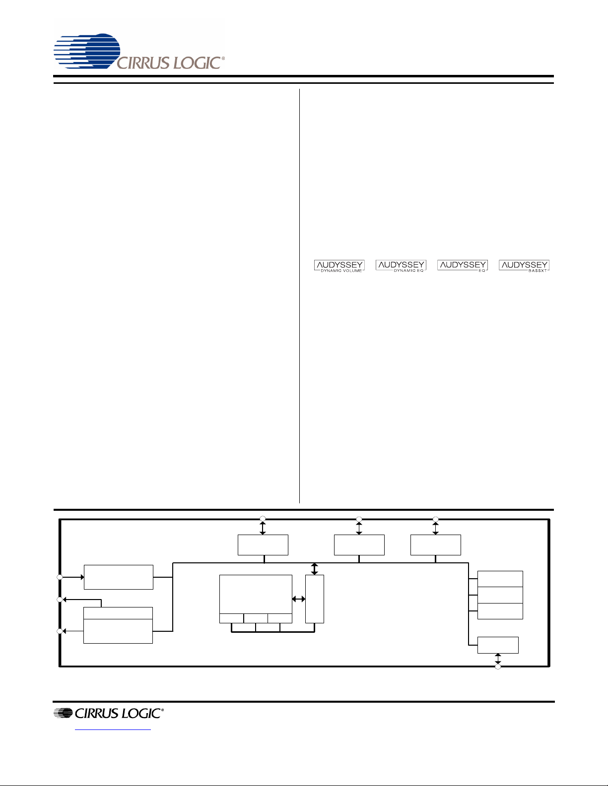
Features: Audyssey Dynamic Volume
TM
, Audyssey EQTM & Audyssey BassXTTM/BassXT-TV
EQ
Audyssey Dynamic Volume eliminates the need for
constant volume adjustments
Audyssey Dynamic EQ enables a reference playback
experience at any desired playback level
Audyssey EQ removes much of the distortion caused by
speaker enclosures and the typical room environment
producing greatly improved sound compared to similar
products without correction
Audyssey BassXT and BassXT-TV are specifically
calibrated to enhance the physical bass respons e of each
product model
Configurable Serial Audio Inputs/Outputs
— Maximum 32-bit @ 192 kHz
(Note: Audyssey Laboratories algorithms support 48 kHz,
44.1 kHz and 32 kHz)
— Integrated 192 kHz capable S/PDIF transmitter
Integrated Clock Manager/PLL
— Can operate from external crystal, external oscillator
Input Fs Auto Detection & Coefficient Loading
Host Control & Boot via Serial Interface
Support for Master (Self) Boot via Serial EEPROM for
single Fs applications (i.e. 48 kHz only via ADC input)
Configurable GPIOs and External Interrupt Input
1.8V Core and a 3.3V I/O that is tolerant to 5V input
Low-power Mode
—“Energy Star® Ready” via low-power mode, 268 µW in
standby
TM
, Audyssey Dynamic
The brand new CS48AU2B device is still based on the same
high-performance 32-bit fixed point Digital Signal Processor
core but instea d is eq uip ped w i th mu ch less memory, tailoring
it for more cost-effective applications which feature Audyssey
Laboratories audio processing technologies. Target
applications are:
TM
— Digital Televisions
—iPod
— A utomotive Head Units (OEM and Aftermarket)
— Automotive Outboard Amplifiers (OEM and Aftermarket)
—Blu-ray
— S oundbars / Sou nd Projectors
The following Audyssey Lab orat orie s al gorithms are currently
supported on the CS48AU2B and more are in development:
While the individual Audyssey processing algorithms have
already been implemented on this DSP, the CS48AU2B is
programmed using the Cirrus proprietary DSP Composer
GUI development tool.
Processing chains combining both standard signal
processing blocks (Tone Control, Bass Management, etc.) in
combination with any combination of Audyssey Laboratories
technology algorithm blocks may be designed using a simple
drag-and-drop interface to create a custom signal flow
specific to your product model. The end result of this is a
software image t hat is d ow n-l oa ded to th e D SP v ia serial host
2
C® or SPITM) or via a serial master (self) boot.
(I
Support for loading of the various Audyssey Laboratories
algorithm coefficient files supplied by Audyssey Laboratories
is easily supported via DSP Composer, enabling the
OEM/ODM to quickly be able to generate the necessary files
for the system microcontroller which have been custom
tailored for each specific model based on the measurement
and analysis performed by Audyssey Laboratories.
Ordering Information:
See page 21 for ordering information
®
Docking Stations
®
L
A
Disc Receivers
FT
DRA
DELPHI
™
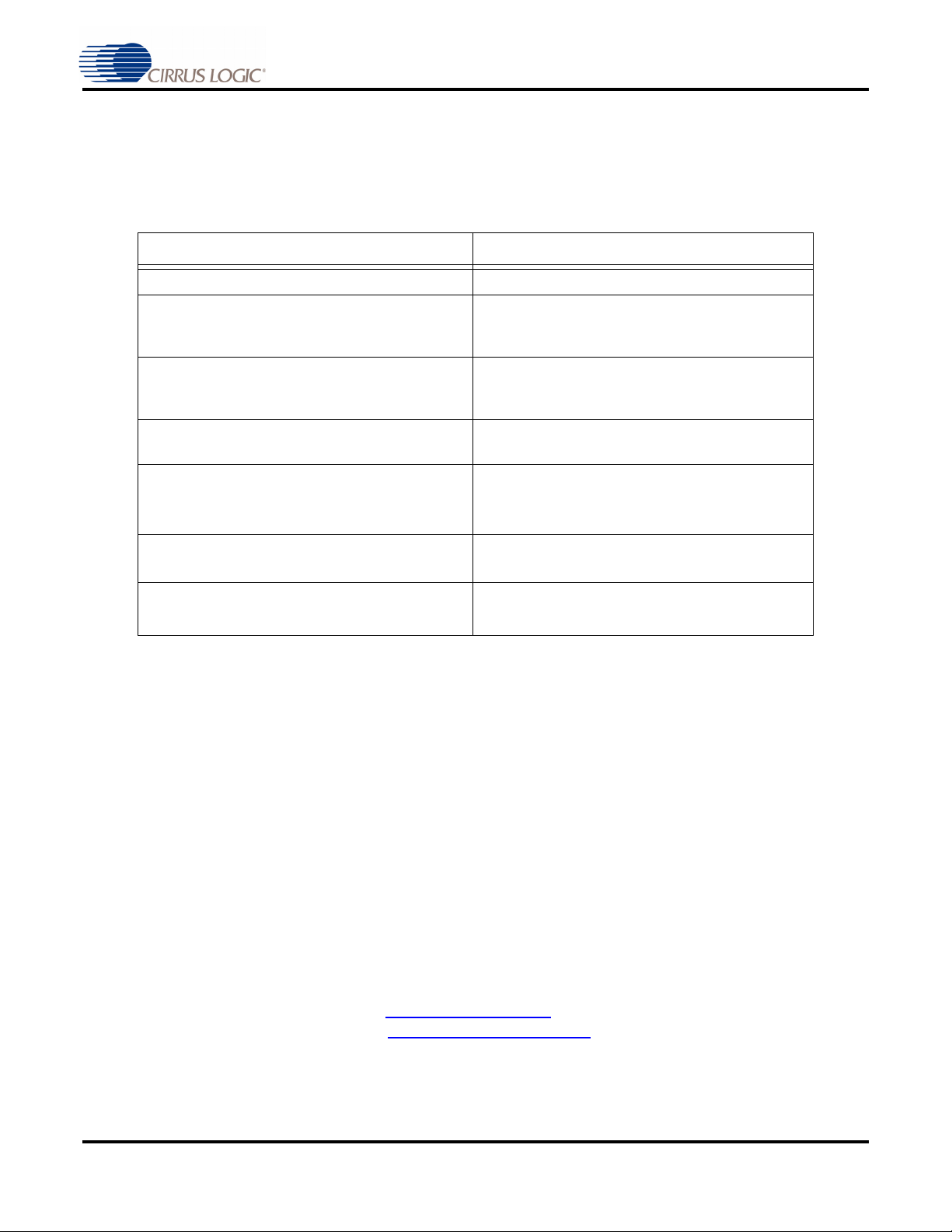
Serial
Control 1
Mu lt ic h ann e l
Audio In
32-bit
S/PDIF
Multichannel
Audio Out
CONFIDENTI
http://www.cirrus.com
DSP
P X Y
Copyright 2009 Cirrus Logic MAY ’09
CONFIDENTIAL DS876F3
D
M
A
GPIO Debug
Watchdog
TMR1
TMR2
PLL
Page 2

CS48AU2B Data Sheet
C
F
T
I
C
t
t
t
i
e
s
s
f
d
p
,
c
s
c
t
d
C
E
P
U
C
C
Y
A
C
F
A
C
n
t
A
h
H
y
L
S
I
i
B
E
Dedicated 32-bit Audio DSP for Audyssey Laboratories Technology
FT
DRA
L
ontacting Cirrus Logic Support
or all product questions and inquiries contact a Cirrus Logic Sales Representative.
o find the one nearest to you go to
MPORTANT NOTICE
irrus Logic, Inc. and i ts subsidiaries (“Cirrus”) bel i eve that the information conta ined i n this document is accurate and rel i abl e . However, the information is sub j ec
o change without notice and i s provided “AS IS” without wa rranty of any kin d (express or impl ied). Customer s are advised to obtain the l atest version o f relevan
nformation to verify, before placing orders, that information being relied on is current and complete. All products are sold subject to the terms and conditions of sal
upplied at the time of order acknowledgment, including those pertaining to warranty, indemnification, and limitation of liability. No responsibility is as sumed by Cirru
or the use of this information, including use of this information as the basis for manufacture or sale of any items, or for infringement of patents or other rights of thir
arties. This document is the property of Cirrus and by furnishing this information, Cirrus grants no license, express or implied under any patents, mask work rights
opyrights, trademarks, trade secr ets or other intell ectual property right s. Cirrus owns the copyright s associated with the informati on contained herei n and give
onsent for copies to be made of the information only for use within your organization with respect to Cirrus integrated circuits or other products of Cirrus. This consen
oes not extend to other copying such as copying for general distribution, advertising or promotional purposes, or for creating any work for resale.
ERTAIN APPLICATIONS USING SEMICONDUCTOR PRODUCTS MAY INVOLVE POTENTIAL RISKS OF DEATH, PERSONAL INJURY, OR SEVER
ROPERTY OR ENVIRONMENTAL DAMAGE (“CRITICAL APPLICA TIONS”). CIRRUS PRODUCTS ARE NOT DESIGNED, AUTHORIZED OR WARRANTED FOR
SE IN PRODUCTS SURGICALLY IMPLANTED INTO THE BODY, AUTOMOTIVE SAFETY OR SECURITY DEVICES, LIFE SUPPORT PRODUCTS OR OTH ER
RITICAL APPLICATIONS. INCLUSION OF CIRRUS PRODUCTS IN SUCH AP PLICATIONS IS UNDERST OOD TO BE FULLY AT THE CUSTOME R'S RISK AND
IRRUS DISCLAIMS AND MAKES NO WARRANTY, EXP RESS , STATUTOR Y OR IMPLIED, INCLUDING THE IMPLIED WARRAN TIES OF ME RCHANTAB ILIT
ND FITNESS FOR PARTICULAR PURPOSE, WITH REGARD TO ANY CIRRUS PRODUCT THAT IS USED IN SUCH A MANNER. IF THE CUSTOMER OR
USTOMER'S CUSTOMER USES OR PERM ITS T HE USE OF CIRRUS PRODUCTS IN CRITICAL APPLICAT IONS , CUSTOMER AGREES, BY SUCH USE, TO
ULLY INDEMNIFY CIRRUS, ITS OFFICE RS, DIRECTORS, EMP LOYEES, DISTRIBUTO RS AND OTHER A GENTS FROM A NY AND ALL L IABILITY, INCLUDING
TTORNEYS' FEES AND COSTS, THAT MAY RESULT FROM OR ARISE IN CONNECT ION WITH THESE USES.
irrus Logic, Cirrus, the Cirrus Logic logo designs, DSP Composer, and Cirrus Framework are trademarks of Cirrus Logic, Inc. All other brand and product names i
his document may be trademarks or service marks of their respective owners.
udyssey, the Audyssey stylized logo and font, Audyssey Dynamic Volume, Audyssey Dynamic EQ, Audyssey EQ, and Audyssey BassXT ( implementations for bot
TIB and TV) are either trad emarks or registered trademarks of Audyssey Labora tories. Sale of the CS48AU2B is only authorized to licensees of Audysse
aboratories deemed to be in good standing.
PI is a trademark of Motorola, Inc.
2
C is a registered trademark of Philips Semiconductor.
Pod is a registered trademark of Apple Computer, Inc.
lu-ray and Blu-ray Disc are trademarks of SONY KABUSHIKI KAISHA CORPORATION.
nergy Star is a registered trademark of the Environmental Protection Agency, a federal agency of the United States government.
2 Copyright 2009 Cirrus Logic DS876F3
CONFIDENTI
www.cirrus.com
.
D
CONFIDENTIAL
A
ELPHI
Page 3

CS48AU2B Data Sheet
Dedicated 32-bit Audio DSP for Audyssey Laboratories Technology
Table of Contents
1. Documentation Strategy . . . . . . . . . . . . . . . . . . . . . . . . . . . . . . . . . . . . . . . . . . . . . . . . . . . . . .5
2. Overview . . . . . . . . . . . . . . . . . . . . . . . . . . . . . . . . . . . . . . . . . . . . . . . . . . . . . . . . . . . . . . . . . . 5
2.1 Licensing . . . . . . . . . . . . . . . . . . . . . . . . . . . . . . . . . . . . . . . . . . . . . . . . . . . . . . . . . . . . . . . . . . . . . . . . . 5
3. Code Overlays . . . . . . . . . . . . . . . . . . . . . . . . . . . . . . . . . . . . . . . . . . . . . . . . . . . . . . . . . . . . . .6
4. Hardware Functional Description . . . . . . . . . . . . . . . . . . . . . . . . . . . . . . . . . . . . . . . . . . . . . .7
4.1 DSP Core . . . . . . . . . . . . . . . . . . . . . . . . . . . . . . . . . . . . . . . . . . . . . . . . . . . . . . . . . . . . . . . . . . . . . . . . 7
4.2 On-chip DSP Peripherals . . . . . . . . . . . . . . . . . . . . . . . . . . . . . . . . . . . . . . . . . . . . . . . . . . . . . . . . . . . . 8
4.3 DSP I/O Description . . . . . . . . . . . . . . . . . . . . . . . . . . . . . . . . . . . . . . . . . . . . . . . . . . . . . . . . . . . . . . . . 9
4.4 Application Code Security . . . . . . . . . . . . . . . . . . . . . . . . . . . . . . . . . . . . . . . . . . . . . . . . . . . . . . . . . . . . 9
5. Characteristics and Specifications . . . . . . . . . . . . . . . . . . . . . . . . . . . . . . . . . . . . . . . . . . . .10
5.1 Absolute Maximum Ratings . . . . . . . . . . . . . . . . . . . . . . . . . . . . . . . . . . . . . . . . . . . . . . . . . . . . . . . . . . 10
5.2 Recommended Operating Conditions . . . . . . . . . . . . . . . . . . . . . . . . . . . . . . . . . . . . . . . . . . . . . . . . . . 10
5.3 Digital DC Characteristics . . . . . . . . . . . . . . . . . . . . . . . . . . . . . . . . . . . . . . . . . . . . . . . . . . . . . . . . . . . 10
5.4 Power Supply Characteristics . . . . . . . . . . . . . . . . . . . . . . . . . . . . . . . . . . . . . . . . . . . . . . . . . . . . . . . . .11
5.5 Thermal Data (48-Pin LQFP) . . . . . . . . . . . . . . . . . . . . . . . . . . . . . . . . . . . . . . . . . . . . . . . . . . . . . . . . .11
5.6 Switching Characteristics— RESET . . . . . . . . . . . . . . . . . . . . . . . . . . . . . . . . . . . . . . . . . . . . . . . . . . . 12
5.7 Switching Characteristics — XTI . . . . . . . . . . . . . . . . . . . . . . . . . . . . . . . . . . . . . . . . . . . . . . . . . . . . . . 12
5.8 Switching Characteristics — Internal Clock . . . . . . . . . . . . . . . . . . . . . . . . . . . . . . . . . . . . . . . . . . . . . . 13
5.9 Switching Characteristics — Serial Control Port - SPI Slave Mode. . . . . . . . . . . . . . . . . . . . . . . . . . . . 13
5.10 Switching Characteristics — Serial Control Port - SPI Master Mode . . . . . . . . . . . . . . . . . . . . . . . . . 14
5.11 Switching Characteristics — Serial Control Port - I
5.12 Switching Characteristics — Serial Control Port - I
5.13 Switching Characteristics — Digital Audio Slave Input Port . . . . . . . . . . . . . . . . . . . . . . . . . . . . . . . . 17
5.14 Switching Characteristics — DSD Slave Input Port . . . . . . . . . . . . . . . . . . . . . . . . . . . . . . . . . . . . . . 17
5.15 Switching Characteristics — Digital Audio Output Port . . . . . . . . . . . . . . . . . . . . . . . . . . . . . . . . . . . . 18
6. Ordering Information . . . . . . . . . . . . . . . . . . . . . . . . . . . . . . . . . . . . . . . . . . . . . . . . . . . . . . .20
7. Environmental, Manufac turi ng, & Handli ng Infor mation . . . . . . . . . . . . . . . . . . . . . . . . . .21
8. Device Pinout Diagram . . . . . . . . . . . . . . . . . . . . . . . . . . . . . . . . . . . . . . . . . . . . . . . . . . . . . .22
8.1 CS48AU2B, 48-pin LQFP Pinout Diagram . . . . . . . . . . . . . . . . . . . . . . . . . . . . . . . . . . . . . . . . . . . . . . 22
9. Package Mechanica l Drawings . . . . . . . . . . . . . . . . . . . . . . . . . . . . . . . . . . . . . . . . . . . . . . .23
9.1 48-pin LQFP Package Drawing . . . . . . . . . . . . . . . . . . . . . . . . . . . . . . . . . . . . . . . . . . . . . . . . . . . . . . . 23
10. Revision History . . . . . . . . . . . . . . . . . . . . . . . . . . . . . . . . . . . . . . . . . . . . . . . . . . . . . . . . . .24
2
C Slave Mode . . . . . . . . . . . . . . . . . . . . . . . . . . . 15
2
C Master Mode . . . . . . . . . . . . . . . . . . . . . . . . . . 16
DRA
L
A
HI
FT
DELP
CONFIDENTI
DS876F3 Copyright 2009 Cirrus Logic 3
CONFIDENTIAL
Page 4

CS48AU2B Data Sheet
Dedicated 32-bit Audio DSP for Audyssey Laboratories Technology
List of Figures
Figure 1. RESET Timing ......................................................................................................................................... 12
Figure 2. XTI Timing ............................................................................................................................................... 12
Figure 3. Serial Control Port - SPI Slave Mode Timing...........................................................................................14
Figure 4. Serial Control Port - SPI Master Mode Timing.........................................................................................15
Figure 5. Serial Control Port - I
Figure 6. Serial Control Port - I
Figure 7. Digital Audio Input (DAI) Port Timing Diagram ........................................................................................ 17
Figure 8. Direct Stream Digital - Serial Audio Input Timing..................................................................................... 18
Figure 9. Digital Audio Output Port Timing, Master Mode.......................................................................................19
Figure 10. Digital Audio Output Timing, Slave Mode (Relationship LRCLK to SCLK)............................................ 19
Figure 11. CS48AU2B, 48-Pin LQFP Pinout .......................................................................................................... 22
Figure 12. 48-Pin LQFP Package Drawing............................................................................................................. 23
2
C Slave Mode Timing ........................................................................................... 16
2
C Master Mode Timing ......................................................................................... 17
List of Tables
Table 1. CS48AU2B Related Documentation........................................................................................................5
Table 2. Device and Firmware Selection Guide.....................................................................................................7
Table 3. Ordering Information..............................................................................................................................20
Table 4. Environmental, Manufacturing, & Handling Information.........................................................................21
FT
DRA
L
A
ELPHI
D
CONFIDENTI
4 Copyright 2009 Cirrus Logic DS876F3
CONFIDENTIAL
Page 5
CS48AU2B Data Sheet
Dedicated 32-bit Audio DSP for Audyssey Laboratories Technology
1. Documentation Strategy
The CS48AU2B Data Sheet describes the CS48AU2B audio processor. This document should be
used in conjunction with the following documents when evaluating or designing a system around the
CS48AU2B of processors.
Table 1. CS48AU2B Related Documentation
Document Name Description
CS48AU2B Data Sheet This document
Includes detai led system des ign information inc luding
CS485xx Hardware User’s Manual
AN298 - CS485xx Firmware User’s Manual
Typical Connection Diagrams, Boot-Procedures, Pin
Descriptions, etc.
Includes detailed firmware design information
including signal processing flow diagram s and cont rol
API information for the operating system.
FT
TM
DSP Composer
AN298PPMQ, Audyssey Dynamic Volume
Audyssey Dynamic EQ
Application Note
AN298PPMR, Audyssey EQ
Application Note
AN298PPMS, Audyssey BassXT
Module Application Note
The scope of the CS48AU2B Data Sheet is primarily the hardware specifications of the CS48AU2B
of devices. This includes hardware functionality, characteristic data, pinout, and packaging
information.
The intended audience for the CS48AU2B Data Sheet is the system PCB designer, MCU
programmer, and the quality control engineer.
2. Overview
The CS48AU2B DSP is designed to provide high-performance post-processing and mixing of digital
audio. The low-power standby preserves battery life for applications which are always on, but not
necessarily processing audio, such as automotive audio systems. The CS48AU2B is available in a
48-pin QFP package. Please refer to Table 2 on page 7 for the input, output and suggested
applications for this device.
User’s Manual
TM
Firmware Module
TM
Firmware Module
TM
Firmware
TM
Includes detailed configuration and usage
information for the GUI development tool.
Contains descriptio n of API used to co ntrol Audysse y
Dynamic Volume and Audyssey Dynamic EQ
firmware.
DRA
Contains descriptio n of API used to co ntrol Audysse y
EQ firmware.
Contains descriptio n of API used to co ntrol Audysse y
BassXT firmware.
L
A
HI
DELP
2.1 Licensing
Licenses are required for any of the Audyssey Laboratories algorithms listed in Section 3. Please
contact Audyssey Laboratories at sales@audyssey.com
technology. Please send e-mail to trademark@audyssey.com
trademarks.
DS876F3 Copyright 2009 Cirrus Logic 5
CONFIDENTI
CONFIDENTIAL
for more information on licensing their
for more information on Audyssey
Page 6

CS48AU2B Data Sheet
Dedicated 32-bit Audio DSP for Audyssey Laboratories Technology
3. Code Overlays
The suite of software avail able fo r t he CS48AU2B consist s o f an o perati ng sys tem (OS) and a l ibrar y
of overlays. The overlays have been divided into three main groups called Matrix-processors,
Virtualizer-processors, and Post-processors. All software components are defined below:
1. OS/Kernel - Encompasses all non-audio processing tasks, including loading data from external
memory, processing host messages, calling audio-processing subroutines, error concealment,
etc.
2. Matrix-processor- Any Module that performs a matrix decode on PCM data to pr oduce mo re
output channels than input channels (2Ön channels). Generally speaking, these modules
increase the number of valid channels in the audio I/O buffer.
3. Virtualizer-processor - Any module that encodes PCM data into fewer output channels than
input channels (nÖ2 channels) with the effect of providing “phantom” speakers to represent the
physical audio channels that were eliminated. Generally speaking, these modules reduce the
number of valid channels in the audio I/O buffer.
4. Post-processors - Any module that processes audio I/O buffer PCM data in-place after the
matrix- or virtualizer -process ors. Examples are bass manag ement, audi o manage r, tone control,
Audyssey Dynamic Volume, Audyssey Dynamic EQ, Audyssey EQ, Audyssey BassXT, delay, &
customer-specific effects, etc.
The certified DSP firmware or application codes provided by Cirrus Logic (under a licensed to you
from Audyssey Laboratories) may enable some or all of the Audyssey Laboratories algorithms.
These licensed processing blocks can be used in combination with a host standard post-processing
signal blocks (tone control, Bass Management, delays, etc.) or lower level primitives such as a filter
or math function.
A product-specific signal flow is generated by the designer using DSP Composer.
L
A
DRA
FT
Once all of the custom coeffic ient fil es supp lied by Audy ssey Lab oratori es have been l oaded and t he
signal flow has been set, the user can perform a “generate delivera bles” inside DSP Composer.
This generates a collection of files that can be easily converted to .c or .h files by the designer for
storage inside the host controller OR can be converted into a small image tha t can either be stored in
an external serial FLASH/EEPROM, or downloaded via a host controller through the
port.
The overlay structure reduces the t ime required t o reconfigu re the DSP when a process ing change is
requested. Each overlay can be reloaded independently without disturbing the other overlays. For
example, when a new matrix-processor is selected, the OS, virtualizer-, and post-processors do not
need to be reloaded — only the new matrix-processor (the same is true for the other overlays).
Table 2 below lists the firmware available based on device selection. Please refer to AN298,
CS485xx Firmware User’s Manual for the latest listing of application codes and Cirrus Framework
modules available.
ELPHI
D
SPI™/I2C
®
serial
™
CONFIDENTI
6 Copyright 2009 Cirrus Logic DS876F3
CONFIDENTIAL
Page 7
Dedicated 32-bit Audio DSP for Audyssey Laboratories Technology
Table 2. Device and Firmware Selection Guide
CS48AU2B Data Sheet
Device
Portable Audio Docking Station
CS48AU2B-CQZ
4. Hardware Functional Description
4.1 DSP Core
The CS48AU2B DSP is a single-core DSP with separate X and Y data and P code memory spaces.
The DSP core is a high-performance, 32-bit, fully user-programmable, fixed-point DSP that is
capable of performing two multiply-an d-acc umulate (MAC) operat i ons per clock cycl e. The DSP core
has eight 72-bit accumulators, four X- and four Y-data register s, and 12 index registers.
The DSP core is coupled to a flexible DMA engine. The DMA engine can move data between
peripherals such as the serial control port (SCP), digital audio input (DAI) and digital audio output
(DAO), or any DSP core memory, all without the intervention of the DSP. The DMA engine off loads
data move instructions from the DSP core, leaving more MIPS available for signal processing
instructions.
Suggested
Application
Digital TV
Portable DVD
DVD Mini / Receiver
Multimedia PC Speakers
8 Channel Car Audio
DVD Receiver
High-end Digital TV
12 channel Car Audio
Channel Count
Input/Output
Up to 12 chann el in /12
channel out
DRA
L
A
HI
Package
48-pin QFP
FT
CS48AU2B functionality is controlled by DSP firmware or application codes that are downloaded to
the CS48AU2B from a host controller or external serial FLASH/EEPROM.
Users can develop their applications using DSP Composer to create the processing chain and then
compile the image into a series of commands that are sent to the CS48AU2B through the SCP. The
processing application can either load modules (matrix-processors, virtualizers, post-processors)
from the DSPs on-board ROM, or custom firmware can be downloaded through the SCP.
4.1.1 DSP Memory
The DSP core has its own on-chip data and program RAM and ROM and does not require external
memory for post-processing applications.
The Y-RAM and P-RAM share a single block of memory that can be configured to make Y and P
equal in size, or more memory can be allocated for Y-RAM in 2kword blocks.
4.1.2 DMA Controller
The powerful 8-channel DMA controller can move data betwee n 8 on-chip resources. Each resource
has its own arbiter: X, Y, and P RAMs/ROMs and the peripheral bus. Modulo and linear addressing
modes are supported, with flexible start address and increment controls. The service intervals for
each DMA channel, as well as up to 6 interrupt events, are programmable.
CONFIDENTI
DELP
DS876F3 Copyright 2009 Cirrus Logic 7
CONFIDENTIAL
Page 8

CS48AU2B Data Sheet
Dedicated 32-bit Audio DSP for Audyssey Laboratories Technology
4.2 On-chip DSP Peripherals
4.2.1 Digital Audio Input Port (DAI)
The DAI port supports a wide variety of data input formats at sample rates (Fs) as high as 192 kHz.
Up to 32-bit word lengths are supported. The DAI also supports a time division multiplexed (TDM)
one-line data mode, that packs PCM audio on a single data line the total number possible depends
on the ratio of SCLK to LRCLK. The CS48AU2B supports up to 8.
The port has two independent slave-only clock domains. Each data input can be independently
assigned to a clock domain. The sample rate of the input clock domains can be determined
automatically by the DSP, off-l oading the t ask of monitor ing the SPDIF receiv er from the host. A time stamping feature allows the input data to be sample-rate converted via software.
4.2.2 Digital Audio Output Port (DAO)
DAO port supports PCM resolutions of up to 32-bits. The port supports sample rates (Fs) as high as
192 kHz. The port can be conf igured as an independent clock domain mastered by the DSP, or as a
clock slave if an external MCLK or SCLK/LRCLK source is available. One of the serial audio pins can
be re-configured as a SPDIF transmitter that drives a bi-phase encoded S/PDIF signal (data with
embedded clock on a single line).
The DAO also supports a time division multiplexed (TDM) one-line data mode, that packs multiple
channels of PCM audio on a single data line.
DRA
4.2.3 Serial Control Port (I
2C®
or SPI™)
FT
The on-chip serial control port is capable of operating as master or slave in either
modes. Master/Slave operation is chosen by mode select pins when the CS48AU2B comes out of
Reset. The serial clock pin can support frequencies as high as 25 MHz in SPI mode ( SPI clock speed
must always be ≤ (F
the communications interface (SCP_BSY
host (SCP_IRQ
4.2.4 GPIO
Many of the CS48AU2B peripheral pins are multiple xed with GPIO. Each GPIO can be configur ed as
an output, an input, or an input with interrupt. Each input-pin interrupt can be configured as rising
edge, falling edge, active-low, or active-high.
4.2.5 PLL-based Clock Generator
The low-jitter PLL generates integer or fractional multiples of a reference frequency which are used
to clock the DSP core and peripherals. Through a second PLL divider chain, a dependent clock
domain can be output on the DAO port for driving audio converters. The CS48AU2B defaults to
running from the external reference frequency and is switched to use the PLL output after overlays
have been loaded and configured, either through master boot from an external FLASH or through
host control. A built-in crystal oscillator circuit with a buffered output is provided. The buffered output
frequency ratio is selectable between 1:1 (default) or 2:1.
4.2.6 Hardware Watchdog Timer
CONFIDENTI
).
/2)). The CS48AU2B serial control port also includes a pin for flow control of
dclk
) and a pin to indicate when the DSP has a message for the
ELPHI
D
L
A
SPI™ or I2C
®
The CS48AU2B has an integrated watchdog timer that acts as a “health” monitor for the DSP. The
watchdog timer must be reset by the DSP before the counter expires, or the entire chip is reset. This
peripheral ensures that the CS48AU2B will reset itself in the event of a temporary system failure. In
stand-alone mode (that is, no host MCU), the DSP will reboot from external FLASH. In slave mode
8 Copyright 2009 Cirrus Logic DS876F3
CONFIDENTIAL
Page 9

CS48AU2B Data Sheet
Dedicated 32-bit Audio DSP for Audyssey Laboratories Technology
(that is, host MCU present) a GPIO will be used to signal the host that the watchdog has expired and
the DSP should be rebooted and re-configured.
4.3 DSP I/O Description
4.3.1 Multiplexed Pins
Many of the CS48AU2B pins are multi-functional. For details on pin functionality please refer to the
CS485xx Hardware User’s Manual.
4.3.2 Termination Requirements
Open-drain pins on the CS48AU2B must be pulled high for proper operation. Please refer to the
CS485xx Hardware User’s Manual to identify which pins are open-drain and what value of pull-up
resistor is required for proper operation.
Mode select pins in the CS48AU2B are used to select the boot mode upon the rising edge from
reset. A detailed explanation of termination requirements for each communication mode select pin
can be found in the CS485xx Hardware User’s Manual.
4.3.3 Pads
The CS48AU2B I/Os operate from the 3.3 V supply and are 5 V tolerant.
FT
4.4 Application Code Security
The external program code may be encrypted by the programmer to protect any intellectual property
it may contain. A secret, customer-specific key is used to encrypt the program code that is to be
stored external to the device. Please contact your local Cirr us representative for det ails.
L
A
DRA
HI
DELP
CONFIDENTI
DS876F3 Copyright 2009 Cirrus Logic 9
CONFIDENTIAL
Page 10

CS48AU2B Data Sheet
Dedicated 32-bit Audio DSP for Audyssey Laboratories Technology
5. Characteristics and Specifications
Note: All data sheet minimum and maximum timing parameters are guaranteed over the rated voltage and
temperature. All data sheet typical parameters are measured under the following conditions: T = 25 °C,
C
= 20 pF, VDD = VDDA = 1.8 V, VDDIO = 3.3 V, GNDD = GNDIO = GNDA = 0 V.
L
5.1 Absolute Maximum Ratings
(GNDD = GNDIO = GNDA = 0 V; all voltages with respect to 0V)
Parameter Symbol Min Max Unit
DC power supplies: Core supply
PLL supply
I/O supply
|VDDA – VDDIO|
Input pin current, any pin except supplies I
Input voltage on PLL_REF_RES V
Input voltage on I/O pins V
Storage temperature T
Caution: Operati on at or bey ond these limits may r esult in permanent dam age to the device. Nor mal operatio n is
not guaranteed at these extremes.
VDD
VDDA
VDDIO
in
filt
inio
stg
-0.3
-0.3
-0.3
-
-+/-10mA
-0.3 3.6 V
-0.3 5.0 V
-65 150 °C
2.0
3.6
3.6
0.3
FT
V
V
V
V
5.2 Recommended Operating Conditions
(GNDD = GNDIO = GNDA = 0 V; all voltages with respect to 0V)
Parameter Symbol Min Typ Max Unit
DC power supplies: Core supply
PLL supply
I/O supply
|VDDA – VDDIO|
Ambient operating temperature
- CQZ
- DQZ
Note: It is recommended that the 3.3 V IO supply come up ahead of or simultaneously with the 1.8 V core supply.
5.3 Digital DC Characteristics
(Measurements performed under static conditions.)
Parameter Symbol Min Typ Max Unit
High-level input voltage V
Low-level input voltage, except XTI V
Low-level input voltage, XTI V
Input Hysteresis V
High-level output voltage (I
Low-level output voltage (I
Input leakage XTI I
Input leakage current (all digital pins with internal
pull-up resist ors enabled)
CONFIDENTI
= -2mA), except XTI V
O
= 2mA), except XTI V
O
I
LEAK
VDDA
VDDIO
ELPHI
D
IH
IL
ILXTI
hys
OH
OL
LXTI
L
VDD
A
T
A
2.0 - - V
--0.8V
--0.6V
VDDIO * 0.9 - - V
- - VDDIO * 0.1 V
--5μA
--70μA
DRA
1.71
3.13
3.13
0
-40
1.8
3.3
3.3
0
-
0.4 V
1.89
3.46
3.46
+70
+85
V
V
V
V
°C
10 Copyright 2009 Cirrus Logic DS876F3
CONFIDENTIAL
Page 11

Dedicated 32-bit Audio DSP for Audyssey Laboratories Technology
5.4 Power Supply Characteristics
(Measurements performed under operating conditions)
Parameter Min Typ Max Unit
Operational Power Supply Current:
VDD: Core and I/O operating
VDDA: PLL operating
VDDIO: With most ports operating
Total Operational Power Dissipation:
Standby Power Supply Current:
VDD: Core and I/O not clocked
VDDA: PLL halted
VDDIO: All connected I/O pins 3-stated by other ICs in system
Total Sta ndby Power Dissipation:
1. Dependent on application firmware and DSP clock speed.
5.5 Thermal Data (48-Pin LQFP)
Junction Temperature
Thermal Resistance (Junction to Ambient)
Thermal Resistance (Junction to Top of Package)
1
Parameter Symbol Min Typ Max Unit
Two-layer Board
Four-layer Board
Two-layer Board
Four-layer Board
1
2
3
4
T
j
θ
ja
ψ
jt
A
-
-
-
-
-
-
-
- - 125
DRA
-
-
63.5
54
L
-
-
0.70
HI
0.64
CS48AU2B Data Sheet
203
8
27
480
100
1
50
348
-
-
-
-
-
-
-
FT
-
-
-
-
mA
mA
mA
mW
μA
μA
μA
μW
°C
°C / Watt
°C / Watt
1. Two-layer board is specified as a 76mm X 114 mm, 1.6 mm thick FR-4 material with 1-oz. copper covering 20 % of the top &
bottom layers.
2. Four-layer board is specified as a 76 mm X 114 mm, 1.6 mm thick FR-4 material with 1-oz. copper covering 20 % of the top &
bottom layers and 0.5-oz. copper covering 90 % of the internal power plane & ground plane layers.
3. To calculate the die temperature for a given power dissipation
T
= Ambient T emperature + [ (Power Dissipation in Watts) * θja ]
j
4. To calculate the case temperature for a given power dissipation
T
= T
- [ (Power Dissipation in Watts) * ψjt ]
c
j
DELP
CONFIDENTI
DS876F3 Copyright 2009 Cirrus Logic 11
CONFIDENTIAL
Page 12

CS48AU2B Data Sheet
A
X
Dedicated 32-bit Audio DSP for Audyssey Laboratories Technology
5.6 Switching Charac teristics— RESET
Parameter Symbol Min Max Unit
RESET
All bidirectional pins high-Z after RESET
Configuration pins setup before RESET
Configuration pins hold after RESET
minimum pulse width low T
low T
high T
high T
RESET
HS[3:0]
ll Bidirectional
Pins
T
rst2z
T
rstl
rstl
rst2z
rstsu
rsthld
T
rstsu
T
1-ms
-100ns
50 - ns
20 - ns
FT
rsthld
DRA
Figure 1. RESET Timing
L
5.7 Switching Characteristics — XTI
Parameter Symbol Min Max Unit
External Crystal operating frequency
XTI period T
XTI high time T
XTI low time T
External Crystal Load Capacitance (parallel resonant)
External Crystal Equivalent Series Resistance ESR - 50 Ω
1
2
A
F
xtal
clki
clkih
clkil
ELPHI
C
L
11.2896 27 MHz
33.3 100 ns
13.3 - ns
13.3 - ns
10 18 pF
D
1. Part characterized with +/- 50 PPM Crystal with the following frequency values:11.2896, 12.288, 18.432, 24.576, and 27 MHz.
2. C
refers to the total load capacitance as specified by the crystal manufacturer. Crystals that require a CL outside this range should
L
be avoided. The crystal oscillator circuit design should follow the crystal manufacturer’s recommendation for load capacitor
selection.
TI
t
clkih
CONFIDENTI
12 Copyright 2009 Cirrus Logic DS876F3
T
clki
Figure 2. XTI Timing
CONFIDENTIAL
t
clkil
Page 13

Dedicated 32-bit Audio DSP for Audyssey Laboratories Technology
5.8 Switching Characteristics — Internal Clock
Parameter Symbol Min Max Unit
Internal DCLK frequency
Internal DCLK period
1. After initial power-on reset, F
the next power-on reset.
1
CS48AU2B-CQZ
1
CS48AU2B-CQZ
= F
dclk
. After initial kickstart commands, the PLL is locked to max F
xtal
F
dclk
DCLKP -
F
6.7 1/F
CS48AU2B Data Sheet
-
xtal
and remains locked until
dclk
MHz
150
ns
xtal
FT
DRA
L
A
HI
DELP
CONFIDENTI
DS876F3 Copyright 2009 Cirrus Logic 13
CONFIDENTIAL
Page 14

CS48AU2B Data Sheet
S
S
Dedicated 32-bit Audio DSP for Audyssey Laboratories Technology
5.9 Switching Charac teristics — Serial Contr ol Port - SPI Slave Mode.
Parameter Symbol Min Typical Max Units
SCP_CLK frequency
SCP_CS
SCP_CLK low time t
SCP_CLK high time t
Setup time SCP_MOSI input t
Hold time SCP_MOSI input t
SCP_CLK low to SCP_MISO output valid t
SCP_CLK falling to SCP_
SCP_CS
SCP_CLK low to SCP_
SCP_CS
SCP_CLK rising t o SCP_BSY
falling to SCP_CLK rising t
rising to SCP_IRQ falling t
rising to SCP_MISO output high-Z t
1. The specification f
maximum speed of the communication port may be limited by the firmware application. Flow control using the SCP_BSY
should be implemented to prevent overflow of the input data buffer. At boot the maximum speed is F
1
IRQ rising t
IRQ rising t
falling t
indicates the maximum speed of the hardware. The system designer should be aware that the actual
spisck
f
spisck
spicss
spickl
spickh
spidsu
spidh
spidov
spiirqh
spiirql
spicsh
spicsdz
spicbsyl
-25MHz
24 - ns
20 - ns
20 - ns
5-ns
5-ns
-11ns
-20ns
0ns
24 - ns
-20 ns
-3
DCLKP+20 ns
*
DRA
xtal
FT
pin
/3.
L
A
56
t
7
spicsh
SCP_CS
SCP_CLK
t
f
spisck
spicss
t
spickl
0
12670
t
spickh
ELPHI
CP_MOSI
CP_MISO
SCP_IRQ
SCP_BSY
CONFIDENTI
A6 A5 A0 R/W MSB LSB
t
spidov
D
MSB
t
spiirqh
LSB
t
spidsu
t
spidh
t
spibsyl
t
spicsdz
t
spiirql
14 Copyright 2009 Cirrus Logic DS876F3
Figure 3. Serial Control Port - SPI Slave Mode Timing
CONFIDENTIAL
Page 15

Dedicated 32-bit Audio DSP for Audyssey Laboratories Technology
S
S
5.10 Switching Characteristics — Serial Control Port - SPI Master Mode
Parameter Symbol Min T ypical Max Units
SCP_CLK frequency
SCP_CS
falling to SCP_CLK rising
1
3
f
spisck
t
spicss
-F
- 11*DCLKP +
(SCP_CLK PERIOD)/2
CS48AU2B Data Sheet
2
/2
xtal
MHz
-ns
SCP_CLK low time t
SCP_CLK high time t
Setup time SCP_MISO input t
Hold time SCP_MISO input t
SCP_CLK low to SCP_MOSI output valid t
SCP_CLK low to SCP_CS
SCP_CLK low to SCP_CS
Bus free time between active SCP_CS
SCP_CLK falling to SCP_MOSI output high-Z t
1. The specification f
maximum speed of the communication port may be limited by the firmware application.
2. See Section 5.7.
3. SCP_CLK PERIOD refers to the period of SCP_CLK as being used in a given application. It does not refer to a tested parameter
falling t
rising t
t
indicates the maximum speed of the hardware. The system designer should be aware that the actual
spisck
spickl
spickh
spidsu
spidh
spidov
spicsl
spicsh
spicsx
spidz
20 - ns
20 - ns
9-ns
5-ns
-8ns
7-ns
- 11*DCLKP +
(SCP_CLK PERIOD)/2
3*DCLKP - ns
-20ns
FT
DRA
L
t
spicsx
t
spicsh
EE_CS
t
spicsl
t
spicss
A
t
0
12670
spickl
56
HI
7
-ns
SCP_CLK
f
spisck
t
spickh
DELP
CP_MISO
CP_MOSI
A6 A5 A0 R/W MSB LSB
t
spidsu
t
spidh
Figure 4. Serial Control Port - SPI Master Mode Timing
t
spidov
MSB
LSB
t
spidz
CONFIDENTI
DS876F3 Copyright 2009 Cirrus Logic 15
CONFIDENTIAL
Page 16

CS48AU2B Data Sheet
S
ft
Dedicated 32-bit Audio DSP for Audyssey Laboratories Technology
5.11 Switching Characteristics — Serial Contr o l Port - I2C Slave Mode
Parameter Symbol Min Typical Max Units
SCP_CLK frequency
SCP_CLK low time t
SCP_CLK high time t
SCP_SCK rising to SCP_SDA risi ng or falling for
START or STOP condition
1
f
iicck
iicckl
iicckh
t
iicckcmd
- 400 kHz
1.25 - µs
1.25 - µs
1.25 µs
START condition to SCP_CLK falling t
SCP_CLK falling to STOP condition t
Bus free time between STOP and START conditions t
Setup time SCP_SDA input vali d to SCP_CLK rising t
Hold time SCP_SDA input after SCP_CLK falling t
SCP_CLK low to SCP_SDA out valid t
SCP_CLK falling to SCP_IRQ
NAK condition to SCP_IRQ
SCP_CLK rising t o SCB_BSY
1. The specification f
maximum speed of the communication port may be limited by the firmware application. Flow control using the SCP_BSY
should be implemented to prevent overflow of the input data buff er.
iicck
rising t
low t
low t
indicates the maximum speed of the hardware. The system designer should be aware that the actual
iicstscl
iicstp
iicbft
iicsu
iich
iicdov
iicirqh
iicirql
iicbsyl
1.25 - µs
2.5 - µs
3-µs
100 ns
20 - ns
-18ns
-3
3*DCLKP + 20 ns
-3*DCLKP + 20 ns
DRA
L
A
t
iicckh
t
iicckl
t
iicr
t
iicdov
t
iicf
6
ELPHI
f
iicck
SCP_CLK
t
iicckcmd
t
iicstscl
01 67801 7
FT
DCLKP + 40 ns
*
pin
t
iicckcmd
8
t
iicstp
t
iicb
SCP_SDA
CP_IRQ
SCP_BSY
CONFIDENTI
16 Copyright 2009 Cirrus Logic DS876F3
A6 A0 R/W ACK
t
iicsutiich
Figure 5. Serial Control Port - I2C Slave Mode Timing
CONFIDENTIAL
D
MSB
t
iicirqh
LSB
t
iiccbsyl
ACK
t
iicirql
Page 17

Dedicated 32-bit Audio DSP for Audyssey Laboratories Technology
S
ft
5.12 Switching Characteristics — Serial Control Port - I2C Master Mode
Parameter Symbol Min Max Units
SCP_CLK frequency
SCP_CLK low time t
SCP_CLK high time t
SCP_SCK rising to SCP_SDA rising or falling for START or
STOP condition
START condition to SCP_CLK falling t
SCP_CLK falling to STOP condition t
Bus free time between STOP and START conditions t
Setup time SCP_SDA input vali d to SCP_CLK rising t
Hold time SCP_SDA input after SCP_CLK falling t
SCP_CLK low to SCP_SDA out valid t
1. The specification f
maximum speed of the communication port may be limited by the firmware application.
1
indicates the maximum speed of the hardware. The system designer should be aware that the actual
iicck
f
iicck
iicckl
iicckh
t
iicckcmd
iicstscl
iicstp
iicbft
iicsu
iich
iicdov
-400kHz
1.25 - µs
1.25 - µs
1.25 µs
1.25 - µs
2.5 - µs
3-µs
100 ns
20 - ns
-18ns
CS48AU2B Data Sheet
FT
CP_CLK
SCP_SDA
t
iicckcmd
t
iicstscl
DRA
t
iicckl
t
iicr
t
iicf
L
01 67801 7
A
t
iicckh
A6 A0 R/W ACK
t
iicsutiich
Figure 6. Serial Control Port - I2C Master Mode Timing
t
iicdov
f
MSB
DELP
6
HI
iicck
LSB
8
ACK
t
t
iicstp
iicckcmd
t
iicb
CONFIDENTI
DS876F3 Copyright 2009 Cirrus Logic 17
CONFIDENTIAL
Page 18

CS48AU2B Data Sheet
D
Dedicated 32-bit Audio DSP for Audyssey Laboratories Technology
5.13 Switching Characteristics — Digital Audio Slave Input Port
Parameter Symbol Min Max Unit
DAI_SCLK period T
DAI_SCLK duty cycle - 45 55 %
Setup time DAI_DATAn t
Hold time DAI_DATAn t
DAI_SCLK
t
daidsu
daiclkp
daidsu
daidh
t
daidh
40 - ns
10 - ns
5-ns
AI_DATAn
Figure 7. Digital Audio Input (DAI) Port Timing Diagram
5.14 Switching Characteristics — DSD Slave Input Port
Parameter Symbol Min Typ Max Unit
DSD_SCLK Pulse Width Low t
DSD_SCLK Pulse Widt h High t
DSD_SCLK Frequency (64x Oversampled) - 1.024 - 3.2 MHz
DSD_A / _B valid to DSD_SCLK rising se tup tim e t
DSD_SCLK rising to DSD_A or DSD_B hold time t
L
sclkl
sclkh
A
sdlrs
sdh
DRA
78 - - ns
78 - - ns
20 - - ns
20 - - ns
FT
ELPHI
D
CONFIDENTI
Figure 8. Direct Stream Digital - Serial Audio Input Timing
18 Copyright 2009 Cirrus Logic DS876F3
CONFIDENTIAL
Page 19

CS48AU2B Data Sheet
D
D
Dedicated 32-bit Audio DSP for Audyssey Laboratories Technology
5.15 Switching Characteristics — Digital Audio Output Port
Parameter Symbol Min Max Unit
DAO_MCLK period T
DAO_MCLK duty cycle - 45 55 %
DAO_SCLK period for Master or Slave mode
DAO_SCLK duty cycle for Master or Slave mode
Master Mode (Output A1 Mode)
DAO_SCLK delay from DAO_MCLK rising edge,
DAO_MCLK as an input
DAO_LRCLK delay from DAO_SCLK transition, respectively
DAO_SCLK delay from DAO_LRCLK transition, respectively
DAO1_DATA[3..0], DAO2_DATA[1..0]
delay from DAO_SCLK transition
Slave Mode (Output A0 Mode)
DAO1_DATA[3..0], DAO2_DATA[1..0]
delay from DAO_SCLK transition
DAO_LRCLK delay from DAO_SCLK transition, respectively
DAO_SCLK delay from DAO_LRCLK transition, respectively
1. Master mode timing specifications are characterized, not production tested.
2. Master mode is defined as the CS48DVxx driving both DAO_SCLK, DAO_LRCLK. When MCLK is an input, it is divided to produce
DAO_SCLK, DAO_LRCLK.
3. This timing parameter is defined from the non-active edge of DAO_SCLK. The active edge of DAO_SCLK is the point at which the
data is valid.
4. Slave mode is defined as DAO_SCLK, DAO_LRCLK driven by an external source.
3
3
1
1
1,2
3
3
4
3
3
daomclk
T
daosclk
-4060%
t
daomsck
t
daomstlr
t
daomlrts
t
daomdv
t
daosdv
t
daosstlr
t
daoslrts
L
A
40 - ns
40 - ns
-19ns
-8ns
-8ns
-10ns
-15ns
-30ns
-15ns
DRA
FT
HI
t
DAO_MCLK
daomlclk
t
DAO_MCLK
daomsck
t
daomclk
t
daomsck
DELP
DAO_SCLK
t
daomdv
AOn_DATAn
t
daomlrts
DAO_LRCLK
CONFIDENTI
Note: In these diagrams, Falling edge is the inactive edge of DAO_SCLK
DS876F3 Copyright 2009 Cirrus Logic 19
CONFIDENTIAL
DAO_SCLK
AOn_DATAn
DAO_LRCLK
t
daomstlr
Page 20

CS48AU2B Data Sheet
D
D
D
v
Dedicated 32-bit Audio DSP for Audyssey Laboratories Technology
Figure 9. Digital Audio Output Port Timing, Master Mode
DAO_LRCLK
DAO_SCLK
AOn_DATAn
Figure 10. Digital Audio Output Timing, Slave Mode (Relationship LRCLK to SCLK)
t
daosstlr
AO_LRCLK
t
daosclk
Note: In these diagrams, Falling edge is the inactive edge of DAO_SCLK
AO_SCLK
t
daoslrts
DRA
L
t
daosclk
t
FT
daosd
A
ELPHI
D
CONFIDENTI
20 Copyright 2009 Cirrus Logic DS876F3
CONFIDENTIAL
Page 21

6. Ordering Infor mation
The CS48AU2B part number is described as follows:
CS48AU2I-XYZR
where
I - ROM ID Number
X - Product Grade
Y - Package Type
Z - Lead (Pb) Free
R - Tape and Reel Packaging
CS48AU2B Data Sheet
Dedicated 32-bit Audio DSP for Audyssey Laboratories Technology
Table 3. Ordering Information
Part No. Grade Temp. Range Package
CS48AU2B-CQZ Commercial 0 to +70 °C 48-pin LQFP
NOTE: Please contact the factory for availability of the -D (automotive grade) package.
DRA
L
A
HI
DELP
FT
CONFIDENTI
DS876F3 Copyright 2009 Cirrus Logic 21
CONFIDENTIAL
Page 22

CS48AU2B Data Sheet
Dedicated 32-bit Audio DSP for Audyssey Laboratories Technology
7. Environmental, Manufacturing, & Handling Information
Table 4. Environmental, Manufacturing, & Handling Information
Model Number Peak Reflow Temp MSL Rating* Max Floor Life
CS48AU2B-CQZ 2 60 °C 3 7 Days
* MSL (Moisture Sensitivity Level) as specified by IPC/JEDEC J-STD-020.
FT
DRA
L
A
ELPHI
D
CONFIDENTI
22 Copyright 2009 Cirrus Logic DS876F3
CONFIDENTIAL
Page 23

Dedicated 32-bit Audio DSP for Audyssey Laboratories Technology
A
8. Device Pinout Diagram
8.1 CS48AU2B, 48-pin LQFP Pinout Diagram
SCP_CLK
CS48AU2B Data Sheet
VDDIO3
SCP_C
GPIO8,
GPOI12, SCP_IRQ
GNDIO4
GPIO13, SCP_BSY , EE_CS
VDD3
XTAL_OUT GPIO15, DAI2_SCLK
GNDA
XTI
XTO
GPIO10, SCP__MISO / SDA
GPIO9, SCP_MOSI
GPIO11,
35
36
37
38
S
39
40
41
42
GND4
33
34
GPIO7, DAO2_D ATA1, HS4
32
GPIO6, DAO2 _DATA0, HS3
31
CS48AU2B
48-Pin
43
LQFP
GPIO5, DAO1_DATA3, X MT
GNDIO3
30
VDD2GND2
28
29
GPIO4, DAO1_ DATA2, HS2
GPIO3, DAO1_ DATA1, HS1
27
DRA
GPIO18, DAO_MCLK
26
25
VDDIO2
24
23
DAO_SCLK
22
GND3
FT
21
DAO_LRCLK
DAO1_DATA0, HS0
20
19
GNDIO2
18
L
44
A
45
46
HI
GPIO14, DAI2_LRCLK
17
16
VDD1
GPIO17, DAI2_DATA0, DSD
15
4
PLL_REF_RES
VDDA (3.3V)
47
48
1
2
3
4
5
6
7
DELP
TEST
RESET
DBDA
GND1
DBCK
GNDIO1
DAI1_LRCLK, DAI1_DATA4, DSD5
9
8
DAI1_SCLK, DSD-CLK
10
GPIO16, DAI1_DATA0, TM0, DSD0
11
DSD1
GPIO0, DAI1_DATA1, TM1,
14
GPIO2, DAI1_DATA3, TM3, DSD3
GPIO1, DAI1_DATA2, TM2, DSD2
13
12
VDDIO1
Figure 11. CS48AU2B, 48-Pin LQFP Pinout
CONFIDENTI
DS876F3 Copyright 2009 Cirrus Logic 23
CONFIDENTIAL
Page 24

CS48AU2B Data Sheet
Dedicated 32-bit Audio DSP for Audyssey Laboratories Technology
9. Package Mechanical Drawings
9.1 48-pin LQFP Package Drawing
48LDLQFP(7x7x1.4mmbody)
FT
DRA
L
A
Number of Leads
MIN NOM MAX
A1.60
A1 0.05 0.15
A2 1.35 1.40 1.45
b 0.17 0.22 0.27
D9.00BSC
D1 7.00 BSC
e0.50BSC
E9.00BSC
E1 7.00 BSC
theta 0 7
L 0.45 0.60 0.75
L1 1.00 REF
NOTES:
1) Reference document: JEDEC MS-026
CONFIDENTI
2) All dimensions are in millimeters and controlling dimension is in millimeters.
3) D1 and E1 do not include mold flash which is 0.25 mm max. per side.A1
4) Dimension b does not include a total allowable dambar protrusion of 0.08 mm max.
48
ELPHI
D
Figure 12. 48-Pin LQFP Package Drawing
24 Copyright 2009 Cirrus Logic DS876F3
CONFIDENTIAL
Page 25

Dedicated 32-bit Audio DSP for Audyssey Laboratories Technology
10. Revision History
Revision Date Changes
F1 December 2, 2008 Initial Release
F2 February 16, 2009 Updated Section 5.5, adding Junction Temperature specification.
F3 May 27, 2009 Updated Note 1 in Section 5.7.
CS48AU2B Data Sheet
FT
DRA
L
A
HI
DELP
CONFIDENTI
DS876F3 Copyright 2009 Cirrus Logic 25
CONFIDENTIAL
Page 26

CS48AU2B Data Sheet
Dedicated 32-bit Audio DSP for Audyssey Laboratories Technology
FT
DRA
L
A
ELPHI
D
CONFIDENTI
26 Copyright 2009 Cirrus Logic DS876F3
CONFIDENTIAL
 Loading...