

CS4812
Fixed Function Multi-Effects Audio Processor
Features
l DSP for embedded reverb/effects
applications
– 24-bit Audio Processing Engine
– No External RAM required
– Two 24-bit ∆Σ ADCs with 100 dB Dyn. Range
– Two 24-bit ∆Σ DACs with 100 dB Dyn. Range
l Mono Guitar or Mixer Effects firmware
included
l Real time parameter control via messaging
protocol
l Serial Control Port for microcontroller
interface
l Single +5V supply operation
l 100-pin Metric Quad Flat Package (MQFP)
ORDERING INFO
CS4812-KM -10 to +70°C 100-pin MQFP
CDB4812 Electric Guitar Effects w/
Parameter Controls.
Description
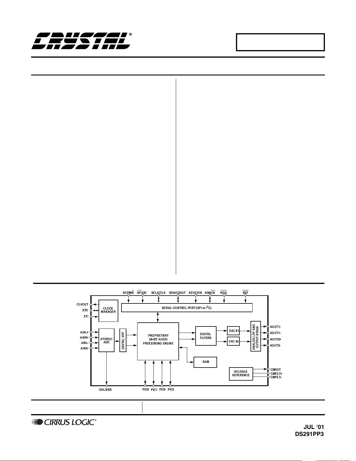
The CS4812 is a complete audio effects processing
system on a chip. This device includes a proprietary 24bit audio processing engine with considerable on-chip
RAM, two ADCs and two DACs. A full-featured serial
control port allows interfacing to an external host
microcontroller. Other features such as single +5V
operation simplify system design.
The CS4812, combined with Crystal effects firmware, is
the ideal solution for a variety of effects processing
applications where user parameter control is desired.
The Crystal effects firmware provides a messaging
protocol for the serial control port that allows an external
microcontroller to have real-time parameter control over
the audio effects. The complete processor and effects
solution may be evaluated with the CDB4812
demonstration board. The CDB4812 demonstrates a
host of mono electric guitar effects including a digital
spring reverb, delay, chorus, flange and tremolo with
parameter adjustment capability. Please refer to AN195
for more information on application firmware for the
CS4812.
I
6&306 63,,& 6&/&&/. 6'$&'287 $'&',1 $'&6 5(4 567
&/.287
;72
;7,
$,1/
$,15
$,1/
$,15
&/2&.
0$1$*(5
67(5(2
$'&
29/(55
Advance Product Information
P.O. Box 17847, Austin, Texas 78760
(512) 445 7222 FAX: (512) 445 7581
http://www.cirrus.com
6(5,$/&21752/325763,RU,&
'
$287
(
)
3
+
/
$
7
,
*
,
'
35235,(7$5<
%,7$8',2
352&(66,1*(1*,1(
3,2
3,2
3,23,2
',*,7$/
),/7(56
5$0
'$&
'$&
92/7$*(
5()(5(1&(
1
*
$
$
)
7
$287
3
6
/
7
*
8
$287
2
3
/
7
$
8
$287
1
2
$
&0287
&0),/7
&0),/7
This document contains information for a new product.
Cirrus Logic reserves the right to modify this product without notice.
Copyright Cirrus Logic, Inc. 2001
(All Rights Reserved)
DS291PP3
JUL ‘01
1

TABLE OF CONTENTS
1. CHARACTERISTICS AND SPECIFICATIONS ........................................................................ 4
2. TYPICAL CONNECTION DIAGRAMS ................................................................................... 14
3. FUNCTIONAL DESCRIPTION ............................................................................................... 17
3.1 Overview .......................................................................................................................... 17
3.2 Analog Inputs ................................................................................................................... 17
3.2.1 Line Level Inputs ................................................................................................. 17
3.2.2 Digital High Pass Filter ........................................................................................ 18
3.3 Analog Outputs ................................................................................................................ 18
3.3.1 Line Level Outputs .............................................................................................. 18
3.4 Clock Generation ............................................................................................................. 19
3.4.1 Clock Source ....................................................................................................... 19
3.5 Serial Control Port ............................................................................................................ 19
3.5.1 SPI Bus ............................................................................................................... 19
3.5.1.1 SPI Master Mode ................................................................................ 20
3.5.1.2 SPI Slave Mode .................................................................................. 20
2
3.5.2 I
3.6 Boot Modes ...................................................................................................................... 26
3.6.1 AutoBoot ............................................................................................................. 26
3.6.2 HostBoot ............................................................................................................. 26
3.7 Resets ............................................................................................................................. 27
4. POWER SUPPLY AND GROUNDING ................................................................................... 28
5. PIN DESCRIPTIONS .............................................................................................................. 29
6. PARAMETER DEFINITIONS .................................................................................................. 33
7. PACKAGE DIMENSIONS ...................................................................................................... 34
C Bus ................................................................................................................ 23
3.5.2.1 I
3.5.2.2 I
CS4812
2
C Master Mode ................................................................................. 23
2
C Slave Mode ................................................................................... 24
LIST OF FIGURES
Figure 1. SPI Control Port Slave Mode Timing .......................................................... 8
Figure 2. SPI Control Port Master Mode (AutoBoot) Timing ..................................... 9
Figure 3. I
Figure 4. I
Figure 5. Typical Connection Diagram, Control Port Slave Mode ........................... 14
Figure 6. Typical Connection Diagram, Control Port I
Figure 7. Typical Connection Diagram, Control Port SPI Master Mode .................. 15
Figure 8. Typical Connection Diagram, Control Port I
Figure 9. Typical Connection Diagram, Control Port SPI Slave Mode .................... 16
Figure 10.Recommended Line Input Buffer .............................................................. 17
Contacting Cirrus Logic Support
For a complete listing of Direct Sales, Distributor, and Sales Representative contacts, visit the Cirrus Logic web site at:
http://www.cirrus.com/corporate/contacts/
Preliminary product information describes products which are in production, but for which full characterization data is not yet available. Advance product information describes products which are in development and subject to development changes. Cirrus Logic, Inc. has made best efforts to ensure that the information
contained in this document is accurate and reliable. However, the information is subject to change without notice and is provided “AS IS” without warranty of any
kind (express or implied). No responsibility is assumed by Cirrus Logic, Inc. for the use of this information, nor for infringements of patents or other rights of third
parties. This document is the property of Cirrus Logic, Inc. and implies no license under patents, copyrights, trademarks, or trade secrets. No part of this publication may be copied, reproduced, stored in a retrieval system, or transmitted, in any form or by any means (electronic, mechanical, photographic, or otherwise)
without the prior written consent of Cirrus Logic, Inc. Items from any Cirrus Logic website or disk may be printed for use by the user. However, no part of the
printout or electronic files may be copied, reproduced, stored in a retrieval system, or transmitted, in any form or by any means (electronic, mechanical, photographic, or otherwise) without the prior written consent of Cirrus Logic, Inc.Furthermore, no part of this publication may be used as a basis for manufacture or
sale of any items without the prior written consent of Cirrus Logic, Inc. The names of products of Cirrus Logic, Inc. or other vendors and suppliers appearing in
this document may be trademarks or service marks of their respective owners which may be registered in some jurisdictions. A list of Cirrus Logic, Inc. trademarks and service marks can be found at http://www.cirrus.com.
2C®
Control Port Slave Mode Timing ...................................................... 11
2C®
Control Port Master Mode (AutoBoot) Timing .................................. 12
2
C Master Mode ................... 15
2
C Slave Mode ..................... 16
2 DS291PP3

Figure 11.Single Ended Input ................................................................................... 18
Figure 12.Butterworth Output Filters ........................................................................ 18
Figure 13.Output Mute Circuit .................................................................................. 19
Figure 14.Control Port Timing, SPI Master Mode AutoBoot ..................................... 20
Figure 15.Control Port Timing, SPI Slave Mode Write ............................................. 20
Figure 16.SPI Slave Write Flow Diagram ................................................................. 21
Figure 17.Control Port Timing, SPI Slave Mode Read ............................................. 21
Figure 18.SPI Slave Mode Read Flow Diagram........................................................ 22
Figure 19.SPI Slave Mode Read Flow Diagram with DSP REQ .............................. 22
Figure 20.Control Port Timing, I
Figure 21.I
2
C Slave Mode Write Flow Diagram ........................................................ 24
Figure 22.Control Port Timing, I
Figure 23.Control Port Timing, I
2
Figure 24.I
Figure 25.I
C Slave Mode Read Flow Diagram ....................................................... 25
2
C Slave Mode Read Flow Diagram with DSP REQ ............................... 26
2
C Master Mode AutoBoot ..................................... 23
2
C Slave Mode Write .............................................. 24
2
C Slave Mode Write .............................................. 24
Figure 26.HostBoot Flow Diagram ........................................................................... 27
Figure 27.CS4812 Suggested Layout ...................................................................... 28
Figure 28.Pin Assignments ...................................................................................... 29
CS4812
DS291PP3 3
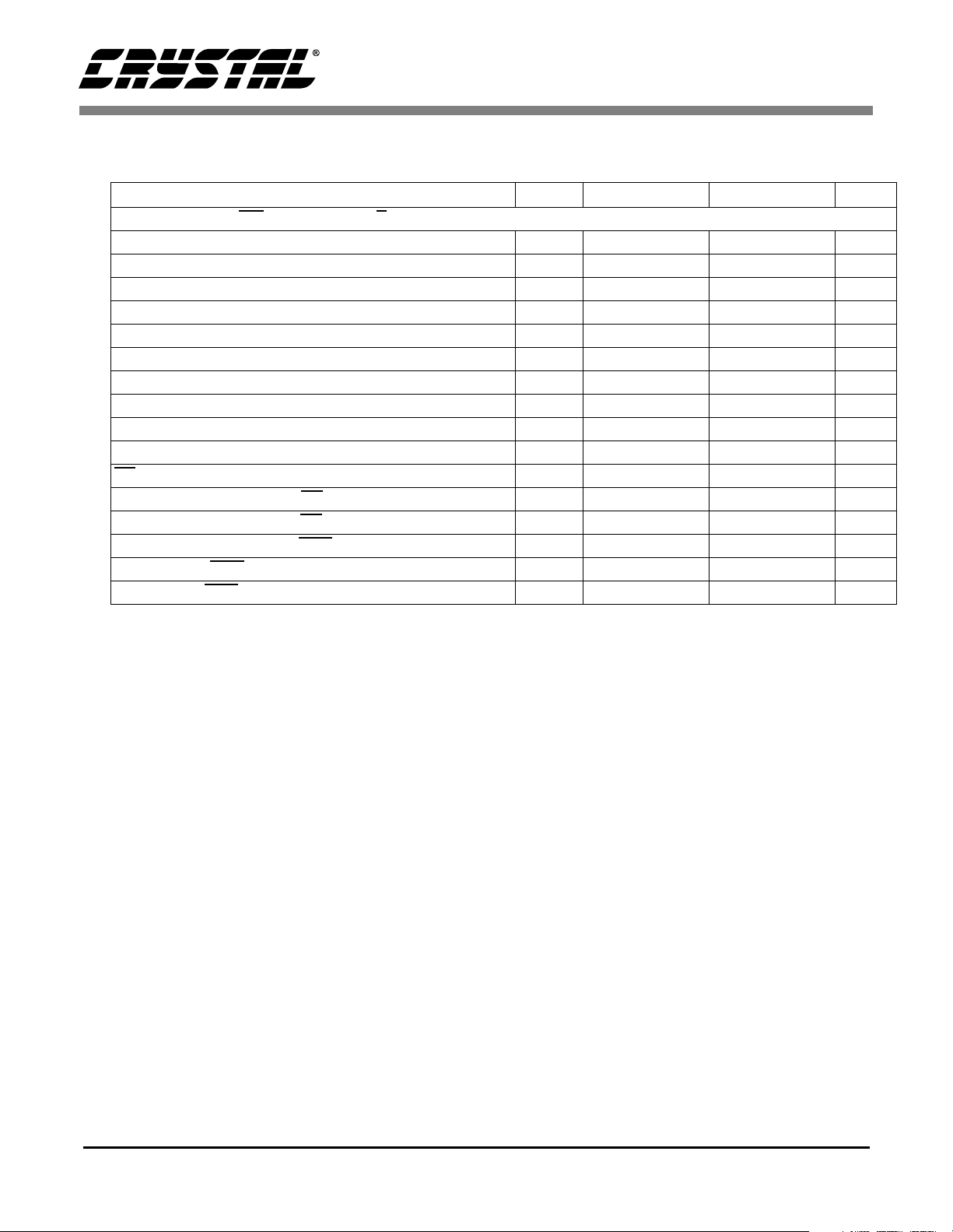
1. CHARACTERISTICS AND SPECIFICATIONS
CS4812
ADC CHARACTERISTICS (T
997 Hz; Fs = 48 kHz; XTI = 12.288 MHz (PLL disabled). Measurement Bandwidth is 20 Hz to 20 kHz.)
Parameters Symbol Min Typ Max Units
Analog Input Characteristics
ADC Conversion Stereo Audio channels 16 - 24 Bits
Dynamic Range (A weighted, Note 5)
(unweighted, Note 5)
Total Harmonic Distortion + Noise (Note 1,5)
(PLL enabled) (Note 1,2,5)
Interchannel Isolation - 90 - dB
Interchannel Gain Mismatch - 0.1 - dB
Offset Error (with high pass filter enabled) (Note 6) - - 0 LSB
Full Scale Input Voltage (Differential) 1.9 2.0 2.1 V
Gain Drift (Note 2) - 100 - ppm/°C
Input Resistance 10 - - kΩ
Input Capacitance - - 15 pF
CMOUT Output Voltage - 2.3 - V
Common Mode Rejection Ratio (Note 2) CMRR 60 dB
Group Delay (Fs = Output Sample Rate) (Note 4) t
Group Delay Variation vs. Frequency ∆t
High Pass Filter Characteristics
Frequency Response -3dB (Note 3)
Phase Deviation @ 20 Hz (Note 3) - 10 - Degree
Passband Ripple - - 0 dB
= 25°C; VA, VD = + 5V; -1 dB Full Scale Input Sine wave,
A
-0.14dB (Note 3)
THD+N -
gd
gd
93
90
-
-15/Fs- s
--0µs
-
-
100
97
-92
-92
3.7
20
-
-
-87
-
-
-
dB
dB
dB
rms
Hz
Hz
Notes: 1. Referenced to typical full-scale differential input voltage (2 V
2. Bench tested only.
3. Filter characteristics scale with output sample rate.
4. Group delay for Fs = 48 kHz, t
5. Measured using differential analog input circuit, see Figure 10.
6. Filter Response is not tested but guaranteed by design.
4 DS291PP3
= 15/48 kHz = 313 µs.
gd
rms
).
CS4812
DAC CHARACTERISTICS (T
997 Hz; Fs = 48 kHz; XTI = 12.288 MHz (PLL disabled). Measurement Bandwidth is 20 Hz to 20 kHz.)
Parameters Symbol Min Typ Max Units
Analog Output Characteristics - Minimum Attenuation, 10 kΩ, 100 pF load; unless otherwise specified.
DAC Resolution 16 - 24 Bits
Dynamic Range (DAC not muted, A weighted) 95 100 - dB
Total Harmonic Distortion + Noise THD+N - -90 -85 dB
Interchannel Isolation - 90 - dB
Interchannel Gain Mismatch - 0.1 - dB
Offset Voltage (differential) (Note 7) - -20 ± 5 - mV
Offset Voltage (V+/V- relative to CMOUT) (Note 7) - -45/-25 - mV
Full Scale Output Voltage (Differential) 1.9 2.0 2.1 V
Gain Drift (Note 2) - 100 - ppm/°C
Out of Band Energy (Fs/2 to 2Fs, Note 2) - -60 - dBFS
Analog Output Load Resistance
Capacitance
Group Delay (Fs = Input Sample Rate) t
Analog Loopback Performance
Signal-to-Noise Ratio (CCIR-2K weighted, -20 dB input) CCIR-2K - 74 - dB
Power Supply
Power Supply Current Operating
Power Down (Note 8)
Power Supply Rejection (1 kHz, 10 mV
= 25°C; VA, VD = + 5V; -1 dB Full Scale Output Sine wave,
A
10
-
gd
, Note 2) - 50 - dB
rms
-16/Fs- s
-
-
-
-
200
1
100
rms
-
-
-
kΩ
pF
mA
mA
Notes: 7. Measured with DAC calibration disabled.
8. Measured with XTI clock disabled.
DS291PP3 5
CS4812
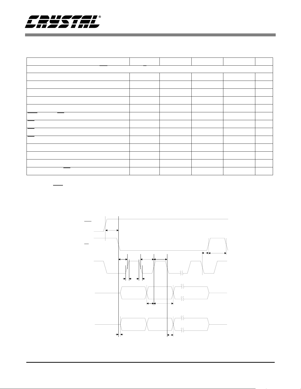
SWITCHING CHARACTERISTICS (T
Parameters Symbol Min Typ Max Units
Audio ADC’s & DAC’s Sample Rate Fs 30 - 50 kHz
XTI Frequency XTI = 128Fs, 256Fs, 512Fs 3.84 - 25.6 MHz
XTI Duty Cycle XTI = 128Fs, 256Fs, 512Fs (Note 9) 40 - 60 %
XTI Jitter Tolerance - 500 - ps
Low Time (Note 10) 500 - - ns
RST
Notes: 9. Guaranteed by characterization but not tested.
10. On power-up, the CS4812 RST
state.
pin should be asserted until the power supplies have reached steady
= 25 °C; VA, VD = +5V, CL = 30 pF)
A
6 DS291PP3
SWITCHING CHARACTERISTICS - CONTROL PORT - SPI SLAVE
(TA = 25 °C; VA, VD = 5 V; Inputs: Logic 0 = DGND, Logic 1 = VD, CL = 30 pF)
Parameter Symbol Min Max Unit
CS4812
SPI Slave Mode (SPI
CCLK Clock Frequency
CCLK Low Time
CCLK High Time
Rise Time of Both CDIN and CCLK Lines
Fall Time of Both CDIN and CCLK Lines
Setup Time CDIN to CCLK Rising
Hold Time CCLK Rising to CDIN (Note 11)
Time from CCLK edge to CDOUT Valid (Note 12)
Rise Time for CDOUT
Fall Time for CDOUT
CS
Falling to CCLK Rising
Time from CCLK Falling to CS
High Time Between Active CS
Time from CCLK Rising to REQ
Rise Time for REQ
Fall Time for REQ
/I2C = 0, SCPM/S = 0, Note 14)
Rising
Rising (Note 13)
f
sck
t
scl
t
sch
t
t
t
cdisu
t
cdih
t
scdov
t
cdor
t
cdof
t
css
t
sccsh
t
csht
t
scrh
t
t
-6MHz
66 - ns
66 - ns
r
f
-100ns
-100ns
40 - ns
15 - ns
-45ns
-25ns
-25ns
20 - ns
0-ns
1-µs
-2*DSPCLK+10ns
rr
rf
-100ns
-100ns
Notes: 11. Data must be held for sufficient time to bridge 100 ns transition time of CCLK.
12. CDOUT should NOT be sampled during this time period.
13. DSPCLK frequency is twice the DSP instruction rate.
14. Timing is guaranteed by characterization. Production test guarantees functionality.
DS291PP3 7

CS4812
A6
csht
t
sccsh
t
7
6
5
LSB
MSB
R/W
A0A6 A5
tri-state
LSB
MSB
cscdo
t
*
rh
t
scdov
t
scdov
t
scrh
t
* See section 3.5.1.2 for a detailed explanation of REQ behavior
Figure 1. SPI Control Port Slave Mode Timing
cdih
t
cdisu
t
rf
t
CDIN
CDOUT
REQ
(output)
CS
sch
t
scl
t
css
t
(input)
f
t
r
t
(input)
SCL/CCLK
8 DS291PP3
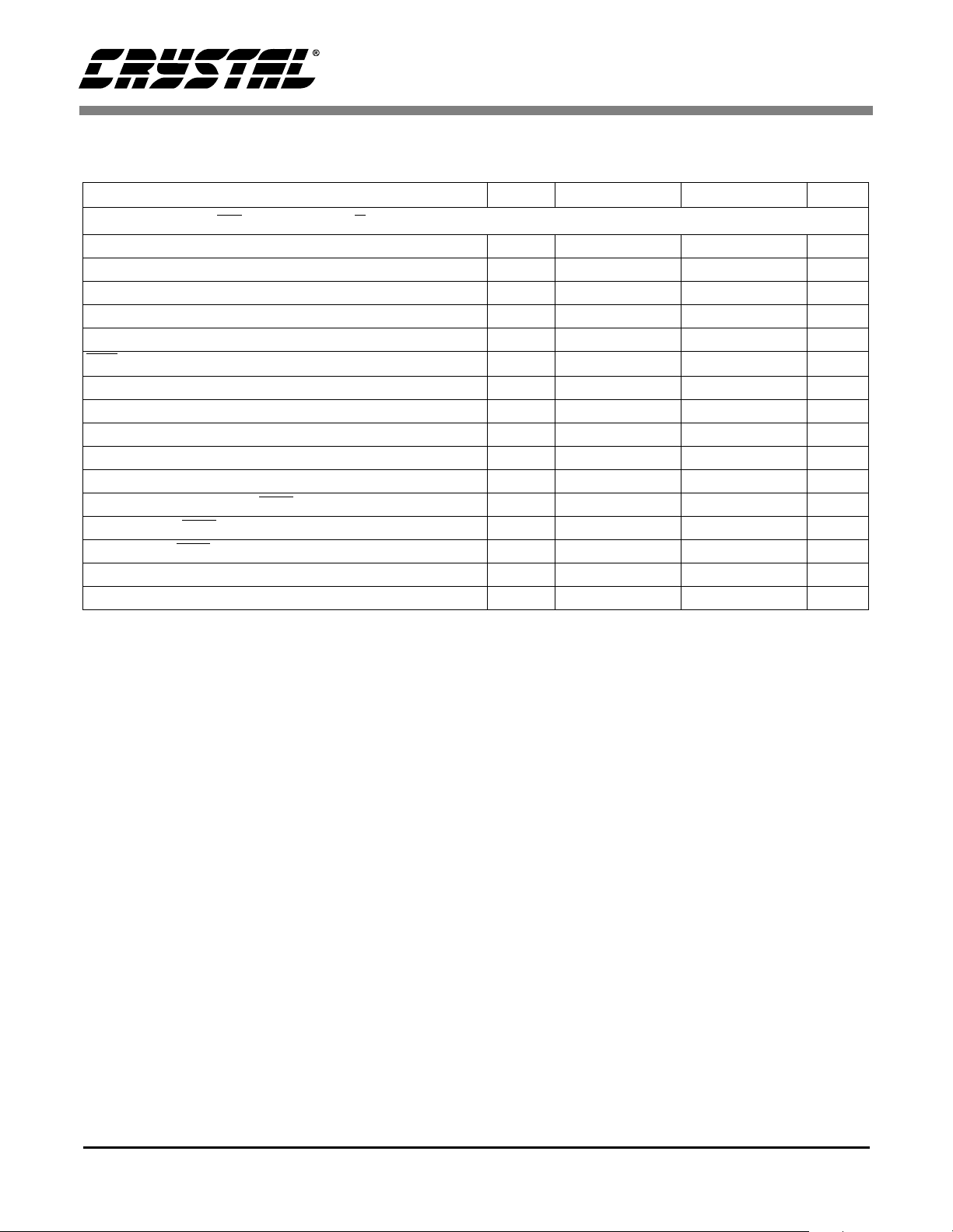
SWITCHING CHARACTERISTICS - CONTROL PORT - SPI MASTER
(TA = 25°C, VA, VD = 5V; Inputs: logic 0 = DGND, logic 1 = VD, CL = 30 pF)
Parameter Symbol Min Typ Max Units
SPI Master (AutoBoot) Mode (SPI
CCLK Clock Frequency (Note 15)
CCLK Low Time
CCLK High Time
CCLK Rise Time (Note 16)
CCLK Fall Time (Note 16)
RST
rising to CS falling
High Time Between Transmissions
CS
CS
Falling to CCLK Edge
CS
Falling to CDOUT valid
CCLK Falling to CDOUT valid
CDIN to CCLK Rising Setup Time
CCLK Rising to DATA Hold Time
CCLK Falling to CS
rising
/I2C = 0, SCPM/S = 1, Note 14)
f
sck
t
scl
t
sch
t
r2
t
f2
t
srs
t
csh
t
css
t
dv
t
pd
t
dsu
t
dh
t
clcs
-Fs-kHz
-1/(2*Fs)-ns
-1/(2*Fs)-ns
-12-ns
-12-ns
-42-µs
37 - - µs
5--µs
- - 50 ns
--100ns
80 - - ns
80 - - ns
40 - - ns
CS4812
Notes: 15. Depending on the input clock configuration, CCLK may be up to 2*Fs temporarily during AutoBoot after
RST
is de-asserted and before the control port registers have been initialized.
16. Measured with a 2.2 kΩ pull-up resistor to VD.
RST
CS
CCLK
CDIN
CDOUT
t
srs
t
css
t
t
t
sch
scl
t
t
f2
dsu
t
dh
t
r2
clcs
t
csh
t
dv
t
pd
Figure 2. SPI Control Port Master Mode (AutoBoot) Timing
DS291PP3 9
SWITCHING CHARACTERISTICS - CONTROL PORT - I2C® SLAVE
(TA = 25 °C; VA, VD = 5 V; Inputs: Logic 0 = DGND, Logic 1 = VD, CL = 30 pF)
Parameter Symbol Min Max Units
2C®
Slave Mode (SPI/I2C = 1, SCPM/S = 0) (Note 17)
I
SCL Clock Frequency
Bus Free Time Between Transmissions
Start Condition Hold Time (prior to first clock pulse)
SCL Low Time
SCL High Time
rising to start condition (Note18)
RST
SDA Hold Time from SCL Falling (Note 19)
Rise Time of Both SDA and SCL
Fall Time of Both SDA and SCL
SCL Falling to CS4812 ACK
SCL Falling to SDA Valid During READ
Time from SCL Rising to REQ
Rising (Note 20)
Rise Time for REQ
Fall Time for REQ
Setup Time for Stop Condition
Setup Time for Repeated Start
f
scl
t
buf
t
hdst
t
low
t
high
t
srs
t
hdd
t
sca
t
scsdv
t
scrh
t
t
t
susp
t
sust
t
r
t
f
rr
rf
-100kHz
4.7 - µs
4.0 - µs
4.7 - µs
4.0 - µs
1-ms
0-µs
-1µs
-300ns
-1.3µs
-1.5µs
-2*DSPCLK+10ns
-100ns
-100ns
4.7 - µs
4.7 µs
CS4812
Notes: 17. Use of the I
Semiconductors.
18. Not tested.
19. Data must be held for sufficient time to bridge the 300 ns transition time of SCL.
20. DSPCLK frequency is twice the DSP instruction rate.
2
C bus interface requires a license from Philips. I2C is a registered trademark of Philips
10 DS291PP3
CS4812
stop
ACK
LSB
MSBA0A6 A5
ACK
R/W
susp
t
8
7
rr
6
scsdv
t
t
80
sca
t
7
*
scrh
t
* See section 3.5.2.2 for a detailed explanation of REQ behavior
f
t
r
(input)
SCL/CCLK
t
high
t
hdd
t
low
t
hdst
t
rf
t
REQ
6
01
sud
t
start
buf
t
stop
SDA
Control Port Slave Mode Timing
®
C
2
Figure 3. I
DS291PP3 11

CS4812
SWITCHING CHARACTERISTICS - CONTROL PORT - I2C® MASTER (T
VA, VD = 5V; Inputs: logic 0 = DGND, logic 1 = VD, C
Parameter Symbol Min Typ Max Units
2C®
I
Master (AutoBoot) Mode (SPI/I2C = 1, SCPM/S = 1) (Note 21)
SCL Clock Frequency (Note 22)
Clock Low Time
Clock High Time
Bus Free Time Between Transmissions
RST
rising to start condition
Start Condition Hold Time
Setup Time for Repeated Start Condition
SDA Setup Time to SCL Rising
SDA Hold Time from SCL Falling (Note 23)
SCL falling to SDA Output Valid
SCL and SDA Rise Time (Note 24)
SCL and SDA Fall Time (Note 24)
Setup Time for Stop Condition
Notes: 21. Use of the I
2
C bus interface requires a license from Philips. I2C is a registered trademark of Philips
Semiconductors.
22. Depending on the input clock configuration, CCLK may be up to 2*Fs temporarily during AutoBoot after
has been de-asserted and before the control port registers have been initialized.
RST
23. Data must be held for sufficient time to bridge the worst case fall time of 300 ns for CCLK/SCL.
24. For both SDA transmitting and receiving.
= 30 pF)
L
f
scl
t
low
t
high
t
buf
t
irs
t
hdst
t
sust
t
sud
t
hdd
t
cldv
t
t
t
susp
-Fs-kHz
-1/(2*Fs)-µs
-1/(2*Fs)-µs
4.7 - - µs
-22-µs
4.0 - - µs
13.5 - - µs
250 - - ns
0--µs
--1.5µs
r
f
--1µs
--300ns
4.7 - - µs
= 25°C;
A
RST
t
SDA
SCL
(output)
irs
Stop Start
t
buf
t
hdst
t
low
t
cldv
t
hdd
t
high
t
sud
Repeated
Start
t
sust
t
hdst
Stop
t
f
t
r
t
susp
Figure 4. I2C® Control Port Master Mode (AutoBoot) Timing
12 DS291PP3

CS4812
ABSOLUTE MAXIMUM RATINGS (All voltages with respect to AGND = DGND = 0V.)
Parameters Symbol Min Typ Max Units
Power Supplies Digital
AnalogVDVA
Input Current (Note 25) - - ±10.0 mA
Analog Input Voltage (Note 26) -0.7 - (VA)+0.7 V
Digital Input Voltage (Note 26) -0.7 - (VD)+0.7 V
Ambient Temperature (Power Applied) -55 - +125 °C
Storage Temperature -65 - +150 °C
Notes: 25. Any pin except supplies. Transient currents of up to ±100 mA on the analog input pins will not cause
SCR latch-up.
26. The maximum over or under voltage is limited by the input current.
Warning: Operation at or beyond these limits may result in permanent damage to the device.
Normal operation is not guaranteed at these extremes.
RECOMMENDED OPERATING CONDITIONS
(All voltages with respect to AGND = DGND = 0V.)
-0.3
-0.3
-
-
6.0
6.0
V
V
Parameters Symbol Min Typ Max Units
Power Supplies Digital
|VA - VD| < 0.4V AnalogVDVA
Operating Ambient Temperature T
DIGITAL CHARACTERISTICS (T
= 25 °C; VA, VD = 5V)
A
A
4.75
4.75
5.0
5.0
5.25
5.25
-10 25 70 °C
Parameters Symbol Min Typ Max Units
High-level Input Voltage (except XTI) V
Low-level Input Voltage (except XTI) V
High-level Output Voltage at I
Low-level Output Voltage at I
= -2.0 mA (except XTO) V
0
= 2.0 mA (except XTO) V
0
High-level Input Voltage (XTI) V
Low-level Input Voltage (XTI) V
IH
IL
OH
OL
IH
IL
2.8 - (VD)+0.3 V
-0.3 - 0.8 V
(VD)-1.0 - - V
--0.4V
2.8 - - V
--2.3V
Input Leakage Current (Digital Inputs) - - 10 µA
Output Leakage Current (High-Z Digital Outputs) - - 10 µA
SWITCHING CHARACTERISTICS - PROGRAMMABLE I/O
(TA = 25 °C; VA, VD = 5V ±5%; Inputs: logic 0 = DGND, logic 1 = VD, CL = 30 pF)
Parameters Symbol Min Typ Max Units
Output Rise Time t
Output Fall Time t
rpo
fpo
-200 -ns
-200 -ns
V
V
DS291PP3 13

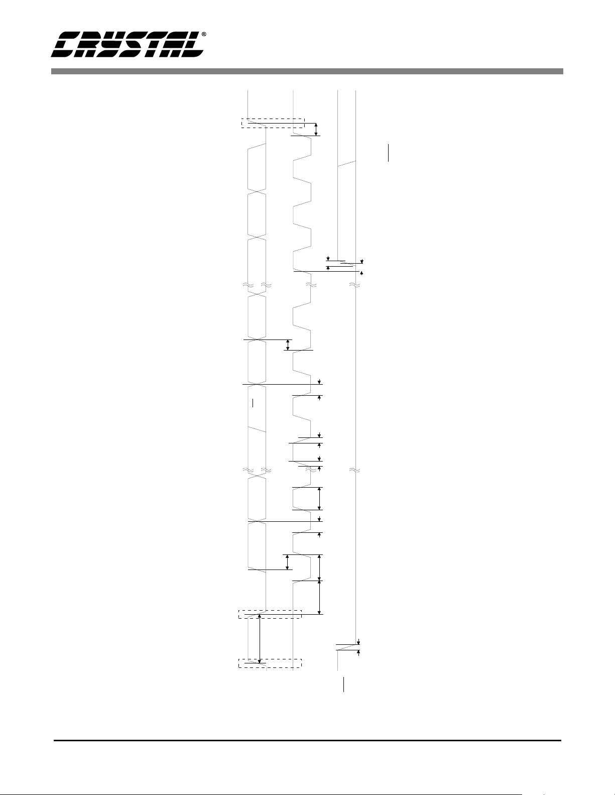
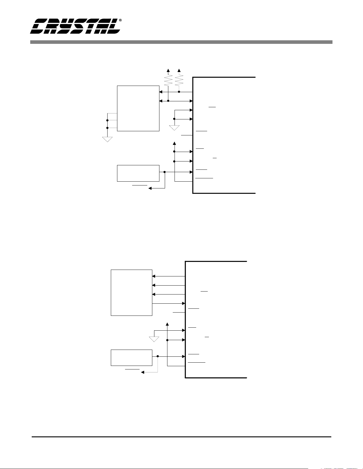
2. TYPICAL CONNECTION DIAGRAMS
12
VA1..3
AIN1L+
AIN1L-
AIN1R+
AIN1R-
ANALOG
FILTER
ANALOG
FILTER
86
87
90
91
1µF
+
AA
8818
0.1µF
Ferr ite Bead
43
VD1..2
+
65
µ
F 0.1µF
1
D
AOUT1+
AOUT1-
AOUT2+
AOUT2-
CS4812
+5 V
D
7
ANALOG
8
FILTER
9
ANALOG
10
FILTER
Program ROM
or
Serial EEPROM
To Optional
Input and
Output Buff ers
Microcontroller
1µF
+
1µF
A
DQ
74HC74
R
S
Mode/Reset
Cir cui t
RESET
Control /
Monit or
Cir cui tr y
R=33
S
All unuse d inputs
should be t ied to gro und.
2.2
K
0.1 µF
VD
D
Ω
0.1 µF
AA
VD
92
39
93
94
2.2
K
63
62
68
67
71
47
69
70
72
41
40
37
35
CMOUT
OVL
CMFILT+
CMFILT-
SCL/CCLK
SDA/CDOUT
AD0/CS
AD1/C DIN
REQ
CLKOUT
SPI/I 2C
SCPM/S
RST
PIO0
PIO1
PIO2
PIO3
AGND1..4
11
13 8919
A
CS4812
DGND1.. 4
42
44
64
D
RES-NC
RES-NC
RES-NC
RES-NC
RES-NC
RES-NC
RES-NC
XTI
45
1 M
39 pF
D
14
15
16
17
20
21
22
23
57
58
59
60
61
95
97
73
32
34
36
38
48
82
83
96
Ω
Optional External
Clock I nput instea d
of Crystal
VD
D
RES-NC
RES-NC
RES-NC
RES-NC
RES-NC
RES-NC
RES-NC
RES-NC
RES-VD
RES-DGND
RES-DGND
RES-DGND
RES-DGND
RES-DGND
RES-DGND
RES-DGND
RES-DGND
XTO
66
46
39 pF
D
Figure 5. Typical Connection Diagram, Control Port Slave Mode
14 DS291PP3
D
EEPROM
A0
A1
A2
Reset
Circuit
2
IC
RESET
2.2 K
VD
D
VD
VD
2.2 K
63
62
68
67
71
69
70
72
73
CS4812
CS4812
SCL/CCLK
SDA/CDOUT
AD0/CS
AD1/CDIN
REQ
SPI/I2C
SCPM/S
RST
PLLEN
Figure 6. Typical Connection Diagram, Control Port
2
I
C Master Mode
CS4812
63
SCL/CCLK
62
SPI
EEPROM
VD
D
Res et
Cir cuit
RESET
68
67
71
69
70
72
73
SDA/CDOUT
AD0/CS
AD1/CDIN
REQ
SPI/I2C
SCPM/S
RST
PLLEN
Figure 7. Typical Connection Diagram, Control Port
SPI Master Mode
DS291PP3 15

CS4812
VD
2.2 K
SDA
SCL
MICRO
CONTROLLER
GPIO
RESET
CIRCUIT
Figure 8. Typical Connection Diagram, Control Port
2
I
C Slave Mode
VD
D
74HC74
R
S
2.2 K
VD
SDA/CDOUT
SCL/CCLK
CLKOUT
AD0/CS
AD1/CDIN
REQ
SPI/I2C
SCPM/S
D
RST
PLLEN
CS4812
CS4812
SDA/CDOUT
SCL/CCLK
CLKOUT
AD0/CS
AD1/CDIN
REQ
SPI/I2C
SCPM/S
RST
PLLEN
CCLK
MICRO
CONTROLLER
RESET
CIRCUIT
MISO
CS
MOSI
GPIO
D
74HC74
R
S
D
VD
Figure 9. Typical Connection Diagram, Control Port
SPI Slave Mode
16 DS291PP3
CS4812
3. FUNCTIONAL DESCRIPTION
3.1 Overview
The CS4812 is a complete audio subsystem on a
chip, integrating an DSP with on-chip RAM, two
24-bit ADCs, two 24-bit DACs, and a serial control
port.
The sigma-delta ADCs include linear phase digital
anti-aliasing filters and only require a single-pole
external passive filter.
The sigma-delta DACs include analog switchedcapacitor anti-image filters and require an external
second or third order active filter that can be easily
integrated into an output differential-to-single-ended converter circuit.
The serial control port is designed to accommodate
I2C® or SPI interfaces and can operate in master or
slave mode. It allows interfacing to external nonvolatile memory for stand-alone operation or to a
host-controller for real-time control. All communications between the DSP and an external EEPROM
or host-controller are handled through the serial
control port.
3.2 Analog Inputs
3.2.1 Line Level Inputs
AINR+, AINR-, AINL+, and AINL- are the line
level analog inputs (See Figure 5). These pins are
internally biased to the CMOUT voltage of 2.3 V.
A DC blocking capacitor placed in series with the
input pins allows signals centered around 0 V to be
input to the CS4812. Figure 5 shows operation with
a single-ended input source. This source may be
supplied to either the positive or negative input as
long as the unused input is connected to ground
through capacitors as shown. When operated with
single-ended inputs, distortion will increase at input levels higher than -1 dBFS. If better performance is required, a single-ended-to-differential
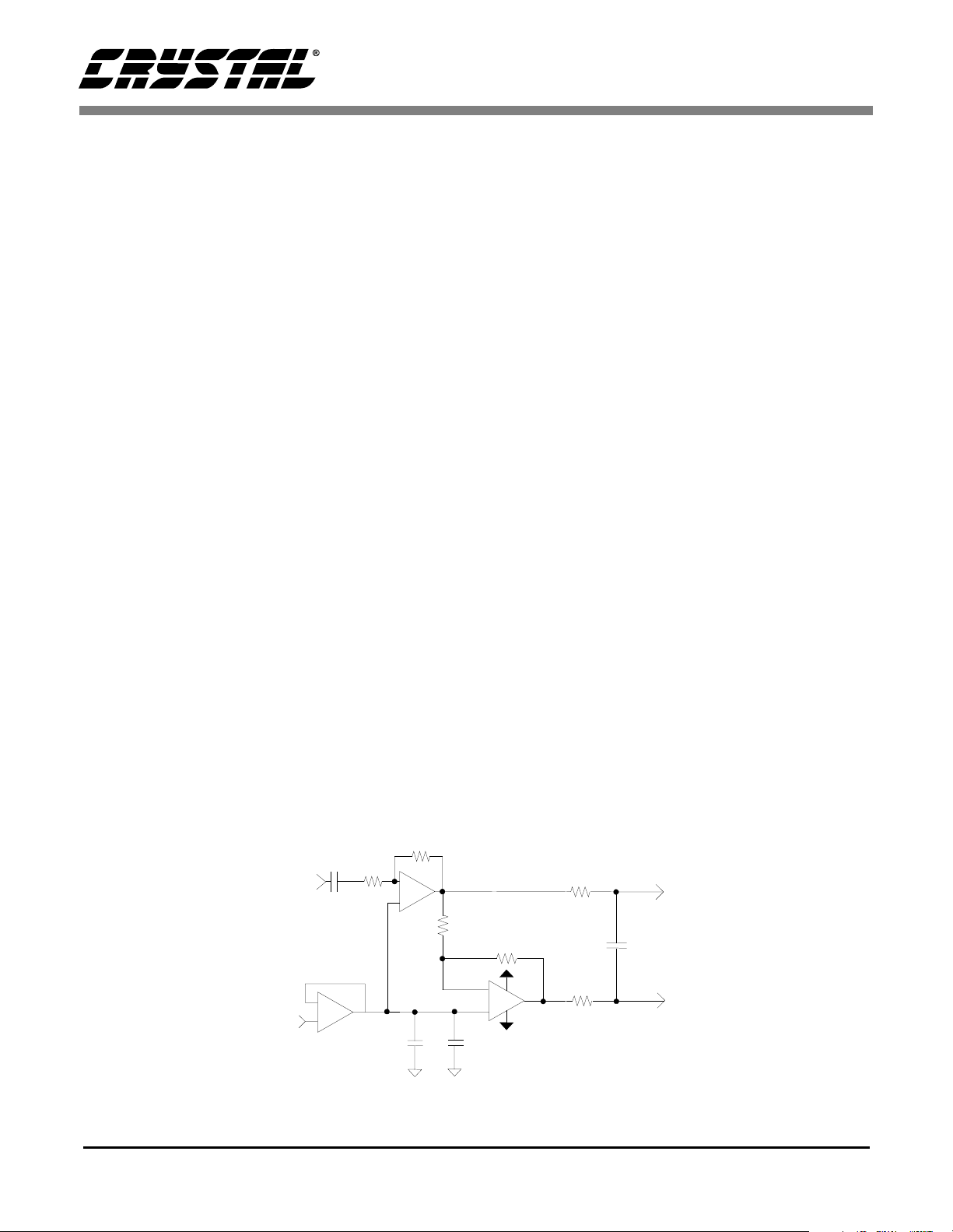
converter, shown in Figure 10, may be used. It provides unity gain, DC blocking and anti-alias filtering.
Inputs may be externally AC or DC coupled. This
permits use of the ADCs for input of audio signals
or for measurement of DC control voltages. By default, an internal high pass filter removes any DC
offsets from both of the ADC inputs. If measurement of DC is required on either of the ADC inputs,
then the on-chip high pass filter must be disabled.
Analog audio input signals that are DC coupled
must be biased at 2.3 V to maintain proper input
4.7 k
10µF
10 k
input signal
(2 Vrms max)
CMOUT
DS291PP3 17
+
-
+
Figure 10. Recommended Line Input Buffer
-
+
10 k
10 k
+5 V
-
+
+
GND
0.1µF10µf
150
AIN -
2.2 nf
150
AIN +
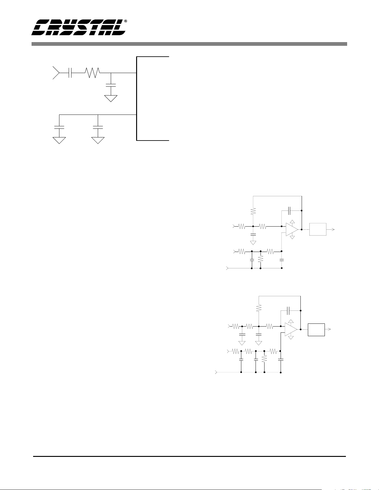
CS4812
CS4812
AIN
AIN
150
22 µF
2.2 nF
100 µF 0.1 µF
+
Ω
Figure 11. Single Ended Input
signal swing. DC control input voltages may range
from ground to Vcc.
ADC output data is in twos-complement binary
format. For inputs above full scale, the ADC digital
output saturates. The OVL output pin asserts when
the analog input is out-of-range.
3.2.2 Digital High Pass Filter
In DC coupled systems, a small DC offset may exist between the input circuitry and the A/D converters. The CS4812 includes a defeatable high pass
filter after the decimator to remove these DC components. The high pass filter response is given in
“High Pass Filter Characteristics” on page 4 and
scales linearly with sample rate. In applications
where DC level measurement is required, as would
occur when one of the ADC inputs is used for measurement of DC control voltages, the high pass filter may be disabled via a control port register.
Note: The high pass filter defeat operates on both
ADC inputs simultaneously therefore external DC
blocking must be provided in the design of the analog audio input circuit.
of driving 10 k
Ω loads to full scale. These amplifi-
ers internally biased to the CMOUT voltage of 2.3
V.
The recommended off-chip analog filter is a second
order Butterworth with a 3 dB corner at Fs. A third
order Butterworth filter with a -3 dB corner at 0.75
Fs can be used if greater out of band noise filtering
is desired. These filters can be easily integrated into
a differential-to-single-ended converter circuit as
shown in the 2-pole and 3-pole Butterworth filters
of Figure 12. The hardware mute circuit referenced
in Figure 12 is shown in Figure 13. Hardware muting is recommended on power-up and powerdown.
220 pF
Ω
14.0 k
+5 V
_
+
GND
Ω
Ω
220
pF
220
pF
Ω
+5 V
Ω
_
+
pF
GND
Ω
220
pF
Ω
Output
Mute Ckt
Output
Mute Ckt
Line
Out
Line
Out
BUFFERED
BUFFERED
CMOUT
CMOUT
A
OU T-
A
OUT+
A
A
OU
OUT+
2200
2200
Ω
T-
2.8k
2.8k
14.0 k
14.0 k
1000
pF
pF
3.24 k
1000
Ω
pF
2-Pole Butterworth Filter
Ω
Ω
11.0k
Ω
Ω
11.0k
pF
2200
Ω
pF
3.24 k
14.0 k
14.0k
2.8k
2200
2.8k
14.0k
3.3 Analog Outputs
3-Pole Butterworth Filter
3.3.1 Line Level Outputs
The CS4812 contains on-chip differential buffer
amplifiers that produce line level outputs capable
18 DS291PP3
Figure 12. Butterworth Output Filters

3.4 Clock Generation
Line Out
VA
From
CS4812
PIO
MMBT3906
MMBT3904
MMBT3906
10 k
Ω
10 k
Ω
10 k
Ω
GND
3.3 k
Ω
10 µF
1 kΩ10 µF
+
From Op-Amp
Figure 13. Output Mute Circuit
The CS4812 master clock may be generated by using the on-chip oscillator with an external crystal or
may be derived from an external clock source.
CS4812
tializes the hardware configuration registers and
downloads the application code to the DSP via 2
dedicated control port registers. Application messaging between the host and the DSP is also done
via these control port registers. The operation of the
control port may be completely asynchronous to
the audio sample rate. However, it is recommended
that the control port pins remain static when not in
use.
The required control port register settings are contained in the Crystal effects firmware application
code EEPROM image.
The control port supports the SPI bus and the I2C
bus in both master and slave modes. The bus interface is selected via the SPI/I2C pin and the master/slave mode is selected via the SCPM/S pin.
These pins are sampled during de-assertion of the
RST pin.
®
3.4.1 Clock Source
The CS4812 requires a 256 Fs master clock to run
the internal logic. The two possible clock sources
are the on-chip crystal oscillator or an external clock
input to the XTI pin.
When using the on-chip crystal oscillator, external
loading capacitors are required. (see Figure 5) High
frequency crystals (>8 MHz) should be parallel
resonant, fundamental mode and designed for
20 pF loading. (equivalent to 40 pF to ground on
each leg)
3.5 Serial Control Port
The serial control port contains all of the main control logic for the chip. It controls power-on sequencing, hardware configuration and DSP
operation. In AutoBoot mode, the serial control
port manages the entire boot process including initialization of its own hardware configuration registers from EEPROM, code download from the
EEPROM to the DSP and initialization of the CODEC. In host-controlled mode, the host-device ini-
Master mode is selected for stand-alone operation
when AutoBooting from an external serial EEPROM. Slave mode is selected when the CS4812 is
connected to an external host controller.
3.5.1 SPI Bus
The SPI bus interface consists of 5 digital signals,
CCLK, CDIN, CDOUT, CS and REQ. CCLK, the
control port bit clock, is used to clock individual data
bits. CDIN, the control data input, is the serial data
input line to the CS4812. CDOUT, the control data
output, is the output data line from the CS4812. It is
Ω
open-drain and requires a 2.2 k
CS, the chip select signal, is asserted low to enable
the SPI port. REQ, the request pin, is used by the
DSP to request a read by a host controller when operating in control port slave mode. Data is clocked
into the chip on the rising edge of CCLK and out on
the falling edge. When in slave mode, the CLK signal must be synchronous with the internal DSP
clock. An external D flip flop off of CLKOUT as
shown in Figure 9 can be used to retime the CLK signal. There is limited drive capability on CLKOUT so
pull-up resistor.
DS291PP3 19

CS4812
a buffer may be required to minimize the capacitive
loading on CLKOUT.
CCLK and CS may be inputs or outputs with respect
to the CS4812. If the serial control port of the
CS4812 is defined as the master, then CCLK and CS
are outputs and CCLK requires a 2.2 kΩ pull-up resistor. If the CS4812 is defined as the slave, then
CCLK and CS are inputs and no pull-up resistor is required on CCLK.
3.5.1.1 SPI Master Mode
The SPI master mode is designed for read-only operation during AutoBooting from a serial EEPROM.
X25650 serial EEPROM, or equivalent, is shown in
Figure 14. On exit from reset, the CS4812 asserts CS.
A typical AutoBoot sequence with a Xicor
CS
0 1 2 21 22 23 24
7 8 9 10 113 4 5 6 30 3125 26 27 28 29
The 8-bit read instruction (00000011) is sent to the
EEPROM followed by a pre-defined 16-bit start address.
The CS4812 then automatically clocks out sequential bytes from the EEPROM until the last byte
has been received.
After the last byte is received, the
CS4812 deasserts CS and begins program execution.
At this point, the serial control port becomes inactive
until the next reset.
3.5.1.2 SPI Slave Mode
In SPI slave mode, a write sequence from an external host controller is shown in Figure 15. The host
controller asserts CS and sends a 16-bit write preamble to the CS4812. This preamble consists of a
7-bit chip address (must be 0010000) followed by
a one-bit R/W (Read/Write) bit (set to 0 for write)
CDOUT
CS
(input)
CLK
(input)
CDIN
(input)
CDOUT
(output)
CLK
CDIN
READ
COMMAND
MSB
ADDRESS = 0X0000
0 0 0 0 0 0 00 0 0 0 0 0 1 1
Figure 14. Control Port Timing, SPI Master Mode AutoBoot
8 9 10 114 5 6 7 0 1 2 3 16 17 18 19 20 21 22
CHIP ADDRESS (WRITE) MAP BYTE
INCR
0 0 1 0 0 0 0 0
MSB
6 5 4 3 2 1 0
R/W
Figure 15. Control Port Timing, SPI Slave Mode Write
16-BIT
7 6 5 4 3 2 1 0
12 13 14 15
DATA
DATA DATA +n
7 6 5 4 3 2 1 0
DATA + n
7 6 5 4 3 2 1 0
23
7 6 5 4 3 2 1 0
20 DS291PP3

CS4812
SET CS LOW
WRITE DATA BYTE
MORE DATA?
SET CS HIGH
Y
WRITE MAP BYTE
N
WRITE ADDRESS BYTE
WITH R/W BIT = 0
Figure 16. SPI Slave Write Flow Diagram
and a memory address pointer (MAP) byte. The
MAP byte contains the address of the control port
register to be accessed. Following the preamble,
the host controller sends the actual data byte to be
written to the register designated by the MAP. The
host controller then de-asserts CS. Figure 16 shows
the SPI slave mode write flow diagram.
In SPI slave mode, a read sequence from an external controller is shown in Figure 17. The host controller executes a partial write-cycle by sending a
16-bit write preamble to the CS4812 with the MAP
byte set to the address of the control port byte register to be read. The host controller then de-asserts
CS, re-asserts CS, and sends the 7-bit chip address
followed by the R/W bit set to 1. The host controller then clocks out the control port register designated by the MAP byte. The host controller then
de-asserts CS. Figure 18 shows the SPI mode slave
read flow diagram initiated by the host microcontroller. Figure 19 shows the SPI slave mode read
flow diagram incorporating the DSP REQ
signal.
REQ is used to notify the host controller that a data
byte from the DSP is waiting to be read.
The behavior of the REQ
signal is dependent on
when data is written to the serial control port output
register in relation to CCLK and bit 2 of the current
byte being transferred. There are three cases of
REQ behavior:
CS
(input)
CLK
(input)
CDIN
(input)
CDOUT
(output)
REQ
(output)
0 0 1 0 0 0 0 0
MSB
0 1 2 3 4 5 6 7 8 9 13 14 15
CHIP ADDRESS (W RITE)
R/W
Figure 17. Control Port Timing, SPI Slave Mode Read
10 11 12
MAP BYTE
INCR
6 5 4 3 2 1 0 0 0 1 0 0 0 0 1
1. The REQ
line will be de-asserted immediately
following the rising edge of CCLK on the D2 bit of
the current byte being transferred if there is no data
in the serial control port output register. The REQ
line remains de-asserted and a stop condition
CHIP ADD RESS (RE AD)
R/W
DATA
7 6 5 4 3 2 1 0
DATA
7 6 5 4 3 2 1 0
DS291PP3 21

SET CS LOW
WRITE ADDRESS BYTE
READ DATA BYTE
MORE BYTES
SET CS HIGH
Y
WRITE ADDRESS BYTE
WRITE MAP BYTE
N
TOGGLE CS
WITH R/W BIT = 0
WITH R/W
BIT = 1
Figure 18. SPI Slave Mode Read Flow Diagram
TO READ?
REQ LOW?
Y
SET CS LOW
WRITE ADDRESS BYTE
WITH R/W BIT = 0
WRITE MAP BYTE FOR
DSP OUTPUT REGISTER
(MAP = 0
X
27)
TOGGLE CS
WRITE ADDRESS BYTE
WITH R/W
BIT = 1
CS4812
N
should be issued by the bus master, thus completing the transfer.
2. If data is written to the serial control port output
register prior to the rising edge of CCLK for the D2
data bit, REQ will remain asserted. The bus master
should continue to shift out this new byte.
3. If data is placed in the SCP output register by the
DSP after the rising edge of CCLK for the D2 bit,
REQ will be immediately re-asserted, thus creating
a pulse on REQ. The byte in the SCP out register
may be read by the bus master as part of the current
transaction or may be read later as part of a new
read transaction.
READ DATA BYTE
FROM DSP OUTPUT REGISTER
REQ STILL LOW?
N
SET CS HIGH
Y
Figure 19. SPI Slave Mode Read from DSP Core
Flow Diagram using DSP REQ
The CS4812 has a MAP auto increment capability
which allows block reads or writes of successive
control port registers.This feature is enabled by setting the INCR bit in the MAP byte.
During a write sequence, multiple bytes may be
written by continuing to send data bytes to the
CS4812 after the first data byte and before de-asserting CS. If auto increment is disabled, the last
data byte sent will appear in the register designated
by the MAP. If auto increment is enabled, data
bytes sent following the first data byte will be written to successive registers following that designated in the MAP.
22 DS291PP3

CS4812
During a read sequence, multiple bytes may be read
by continuing to clock out data bytes to the CS4812
after the first data byte and before de-asserting CS.
If auto increment is disabled, the last data byte read
will be the register designated by the MAP. If auto
increment is enabled, data bytes read following the
first data byte will be read from successive registers
following that designated in the MAP.
3.5.2 I2C Bus
The I2C bus interface implemented on the CS4812
consists of 3 digital signals, SCL, SDA and REQ.
SCL, or serial clock, is used to clock individual
data bits. SDA, or serial data, is a bidirectional data
line. REQ, the request pin, is used by the DSP to request a host read when operating in control port
slave mode. Two additional pins, AD1 and AD0,
are inputs which determine the 2 lowest order bits
of the 7-bit I2C device address.
SCL may be defined as an input or an output with
respect to the CS4812. If the serial control port of
the CS4812 is defined as the master, then SCL is an
open-drain output and requires a pull-up resistor as
shown in Figure 5. Conversely, if the serial control
port of the CS4812 is defined as the slave, then
SCL is an input.
SDA carries time-multiplexed bidirectional serial
data. It is open-drain and requires a pull-up resistor
as shown in Figure 5.
AD1 and AD0, the inputs which determine the 2
lowest order bits of the 8-bit I2C device address, are
meaningful only when the CS4812 is operating as
a slave device and may be tied to ground when the
CS4812 is configured for master mode.
When operating in control port slave mode, the
REQ
output pin is used by the CS4812 DSP to re-
quest communication with the master.
3.5.2.1 I2C Master Mode
The I2C master mode is designed for read-only operation during AutoBooting from a serial EEPROM. A typical AutoBoot sequence with a
Microchip X24256 serial EEPROM, or equivalent,
is shown in Figure 20. On exit from reset, the
CS4812 sends an initial write preamble to the EEPROM which consists of a I2C start condition and
the slave address byte. The slave address consists
of the 4 most significant bits set to 1010, the following 3 bits corresponding to the device select
bits, A2, A1 and A0 set to 000 and the last bit (R/W)
set to 0. Following this, a 2-byte EEPROM starting
address of 0x0000 is sent to the EEPROM. The 2byte EEPROM starting address uses only the lowest 13 bits and sets the highest 3 bits to zero. To begin reading from the EEPROM, the CS4812 sends
another start condition followed by a read preamble. The read preamble is identical to the write preamble except for the state of the R/W bit. The
CS4812 then automatically clocks out sequential
bytes from the EEPROM until the last byte has
been received. These bytes include initial values
for all control port registers as well as the DSP application code. After the last byte, the CS4812 initiates a stop condition and begins program
execution. At this point, the serial control port becomes inactive until the next reset. Actual EE-
0 1 2 3
SCL
CHIP ADDRESS (WRITE) CHIP ADDRESS (READ)MEMORY ADDRESS DATA DATA +n
SDA
DS291PP3 23
1 0 1 0 A2 A1 A0 0 0 0 0 0 0 0 1 0 1 0 A2 A1 A0 1
START
4 5 6 7
ACK NO
Figure 20. Control Port Timing, I2C Master Mode AutoBoot
16 17 18 19 25 26 27 28 29
ACK
START STOP
34 35 36 3730 31 32 338 9 10
7 0
ACKACK
7 0
ACK

PROM memory mapping is handled automatically
by the development tools and is transparent to the
designer.
3.5.2.2 I2C Slave Mode
In I2C slave mode, a write sequence from an external host controller is shown in Figure 22.. The host
controller sends a write preamble consisting of a
start condition followed by the slave address for the
CS4812. The slave address byte consists of a 7-bit
address field (00100|AD1|AD0) followed by a
Read/Write bit (set to 0). AD1 and AD0 correspond
to the logic levels applied to the these pins on the
CS4812. The host controller then sends a MAP
byte which contains the address of the control register to be accessed followed by the actual data byte
to be written to the register designated by the MAP.
Upon completion of this, the host controller then
sends a stop condition to complete the transaction.
Figure 21 shows the I2C slave mode write flow diagram
2
C slave mode, a read sequence by an external
In I
host controller is shown in Figure 23. The host controller sends a write preamble to the CS4812 which
CS4812
SEND I2C START
WRITE ADDRESS BYTE
WITH R/W
SEND MAP BYTE
SEND DATABYTE
SEND I2C STOP
Figure 21. I2C Slave Mode Write Flow Diagram
BIT = 0
GET ACK
GET ACK
GET ACK
MORE DATA?
N
Y
0 1 2 3 8 9 12 16 17 18 1910 11 13 14 15 27 28
4 5 6 7 24 25
26
SCL
SDA
CHIP ADDRESS (WRIT E) MAP BYTE DATA
0 0 1 0 0 AD1 AD0 0
START
DATA +1
INCR
6 5 4 3 2 1 0 7 6 1 0 7 6 1 0 7 6 1 0
ACK
DATA +n
ACKACKACK
STOP
Figure 22. Control Port Timing, I2C Slave Mode Write
168 9 12 13 14 154 5 6 7 0 1 20 21 22 23 24
CHIP ADDRESS (READ)
0 0 1 0 0 AD1 AD0 1
ACK
START
26 27 28
DATA +1
7 0 7 0 7 0
ACK
ACK
DATA + n
NO
STOPACK
SCL
SDA
REQ
CHIP ADDRESS (WRITE)
0 0 1 0 0 AD1 AD0 0
START
2 3 10 11 17 18 19 25
MAP BYTE DATA
INCR
6 5 4 3 2 1 0
ACK
Figure 23. Control Port Timing, I2C Slave Mode Read
24 DS291PP3

consists of a start condition followed by its slave
address byte with the Read/Write bit set to 0. The
host controller then initiates a read preamble. The
read preamble is identical to the write preamble except for the state of the Read/Write bit. The host
controller then sends a MAP byte which contains
the address of the control register to be accessed.
After receiving the MAP byte, the CS4812 returns
the contents of this register to the host controller.
The host controller may continue reading registers
by sending additional MAP bytes or complete the
transaction by initiating a stop condition. Figure 24
shows the SPI mode slave read flow diagram initiated by the host microcontroller. Figure 25 shows
2
C slave mode read flow diagram incorporat-
the I
ing the DSP REQ signal. REQ is used to notify the
host controller that a data byte from the DSP is
waiting to be read.
The behavior of the REQ
signal is dependent on
when data is written to the SCP output register in
relation to SCL and bit 1 of the current byte being
transferred. There are three cases of REQ behavior:
SEND I2C START
WRITE ADDRESS BYTE
WITH R/W BIT = 0
GET ACK
SEND MAP BYTE
GET ACK
SEND I2C START
WRITE ADDRESS BYTE
WITH R/W
BIT = 1
GET ACK
CS4812
1. The REQ
line will be de-asserted immediately
following the rising edge of SCL on the D1 bit of
the current byte being transferred if there is no data
in the SCP output register. The REQ line remains
de-asserted and a stop condition should be issued
by the bus master, thus completing the transfer.
2. If data is written to the SCP output register prior
to the rising edge of SCL for the D1 bit, REQ will
remain asserted. The bus master should continue to
shift out this new byte.
3. If data is placed in the SCP output register by the
DSP after the rising edge of SCL for the D1 bit,
REQ will be immediately re-asserted, thus creating
a pulse on REQ. The byte in the SCP out register
may be read by the bus master as part of the current
transaction or may be read later as part of a new
read transaction.
The CS4812 has a MAP auto increment capability
which allows block reads or writes of successive
READ DATABYTE
MORE BYTES
TO READ?
N
SEND NACK
SEND I2C STOP
Figure 24. I2C Slave Mode Read Flow Diagram
Y
SEND ACK
control port registers.This feature is enabled by setting the INCR bit in the MAP byte.
During a write sequence, multiple bytes may be
written by continuing to send data bytes to the
CS4812 after the first data byte and before initiating a stop condition. If auto increment is disabled,
the last data byte sent will appear in the register
designated by the MAP. If auto increment is en-
DS291PP3 25

Figure 25. I2C Slave Mode Read from DSP Core
Flow Diagram with DSP REQ
N
REQ LOW?
Y
SEND I2C START
WRITE ADDRESS BYTE
WITH R/ W
BIT = 0
GET ACK
READ DATABYTE
REQ STILL LOW?
N
Y
SEND ACK
SEND NACK
SEND I2C STOP
GET ACK
WRITE ADDRESS BYTE
WITH R/W
BIT = 1
GET ACK
SEND I2C START
SEND MAP BYTE
CS4812
abled, data bytes sent following the first data byte
will be written to successive registers following
that designated in the MAP.
During a read sequence, multiple bytes may be read
by continuing to clock in data bytes to the CS4812
after the first data byte and before initiating a stop
condition. If auto increment is disabled, the last
data byte read will be the register designated by the
MAP. If auto increment is enabled, data bytes read
following the first data byte will be read from successive registers following that designated in the
MAP.
3.6 Boot Modes
There are two different techniques that allow the
system to load the application code into the
CS4812. The first technique is called, “AutoBoot”
and allows the application code to be loaded from
an external serial EEPROM with an I2C or SPI interface. This technique is used in system applications that due not have a host. The second
technique is called, “Host Boot” and allows the application code to be loaded directly from the host
microcontroller via I2C or SPI communication interface. This method may eliminate the need for an
external EEPROM.
3.6.1 AutoBoot
The AutoBoot method simply requires an external
EEPROM with an I2C or SPI serial bus interface.
The DSP, automatically loads and runs the application code resident in the EEPROM upon deassertion of the RESET line. It should be noted that this
technique is used for systems that do not have a microcontroller and do not require real-time adjustment of the application code parameters. Please
refer to Table 10 on page 6 for the timing requirements of the RESET line.
3.6.2 HostBoot
By using the HostBoot technique, an external microcontroller is required to download the applica-
26 DS291PP3

tion code. This technique allows for real-time
control of all parameters specific to the application
code. Please refer to Figure 26 for the HostBoot
procedure flow chart and to Section 1.2.1 of
AN195 for an example of a host boot sequence.
3.7 Resets
SEND APPLICATION
SPECIFIC CONTROL PORT
CONFIG BYTES
WRITE BYTE 0XA4
TO CONTROL PORT
REGISTER 4 (MAP = 4)
CS4812
There are several reset mechanisms in the CS4812
which affect different parts of the chip. Full chip reset can only be achieved by asserting the external
RST pin. With RST asserted, the chip enters low
power mode during which the control port, CODEC and DSP are reset, all registers are returned to
their default values and the DAC outputs are muted. The RST pin should be asserted during powerup until the power supplies have reached steady
state.
If the supply voltage drops below 4 Volts, the CODEC is reset, the DAC outputs are muted and the
DSP automatically executes a soft reset.
Upon exit from a CODEC reset, the DSP restarts
the application code and the CODEC performs the
following procedure:
– The CODEC resynchronizes.
– The DAC outputs unmute.
WRITE BYTE 0XA5
TO CONTROL PORT
REGISTER 4
WRITE BYTE 0XA7
TO CONTROL PORT
REGISTER 4
SEND 3 BYTE MESSAGE TO
THE DSP INPUT REGISTER
(MAP = 3) :0X000004
WAIT FOR REPLY FROM DSP
(REQ LINE GOES LOW)
READ REPLY BYTE FROM DSP
OUTPUT REGISTER (MAP = 27)
REPLY BYTE
= 0
X
01?
Y
WRITE .LDT FILE INTO
DSP INPUT REGISTER (MAP = 16)
(LOAD APPLICATION CODE)
N
REQ
LOW?
Y
READ REPLY BYTE FROM DSP
OUTPUT REGISTER (MAP = 27)
REPLY BYTE
= 0X02?
Y
SEND 3 BYTE MESSAGE TO
THE DSP INPUT REGISTER
(MAP = 16):0X000005
WRITE BYTE 0XA6
TO CONTROL PORT
REGISTER 4
N
N
Figure 26. HostBoot Flow Diagram
DS291PP3 27
CS4812
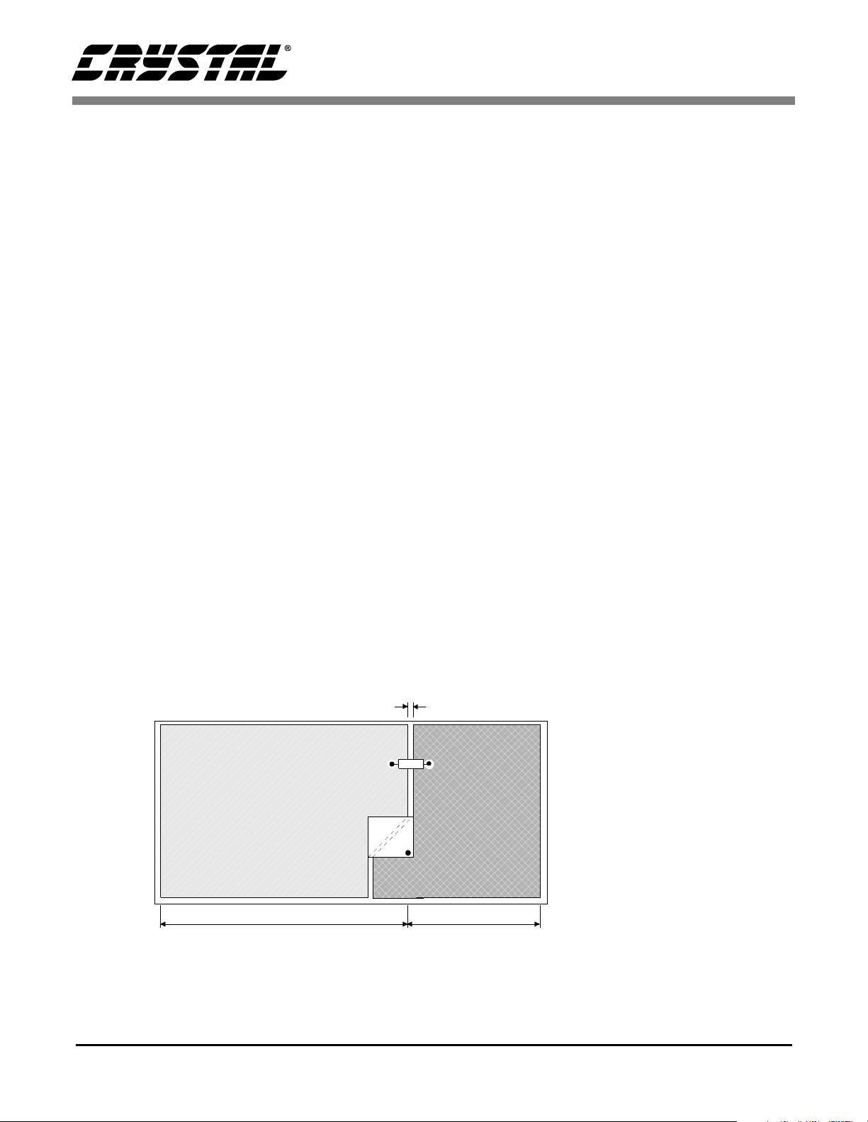
4. POWER SUPPLY AND GROUNDING
Proper layout and grounding is critical to obtaining
optimal audio performance in your system. The
most important rule to remember is to not allow
currents from digital circuitry to couple into sensitive analog circuitry. This is generally done by using a separate or filtered power supply for the
analog circuitry, physically separating the analog
and digital components and traces in the pcb layout
and using wide traces or planes for ground and
power. One misplaced component or trace can severely degrade overall system performance.
When using separate supplies, the analog and digital power should be connected to the CS4812 via a
ferrite bead, positioned closer than 1" to the device
(see Figure 21). The CS4812 VA pin should be derived from the quietest power source available. If
only one supply is available, use the suggested arrangement in Figure 5.
A single solid ground plane is the simplest grounding scheme that works well in many cases. All analog and digital grounds shown in Figure 5 should
be tied to the one plane.
Decoupling capacitors should be placed as close as
possible to the device with the lowest value capacitor closest to the chip. Any power and ground connection vias should be placed near their respective
component pins and should be attached directly to
the appropriate plane. If traces are used for the
power supplies to the CS4812, they should be as
wide as possible to maintain low impedance.
It is recommended to solder the CS4812 directly to
the printed circuit board. Soldering improves performance and enhances reliability
>
1/8"
Digital
Power
Plane
Digital Interface
Figure 27. CS4812 Suggested Layout
28 DS291PP3
Ferrite
Bead
CS4812
Analog Signals &
Components
Analog
Power
Plane
Note that the CS4812
is oriented with its
digital pins towards the
digital end of the board.

5. PIN DESCRIPTIONS
CS4812
DGND
AD1/CDIN
AD0/CS
SPI/I2C
SCPM/S
REQ
RST
RES-VD
NC
NC
NC
NC
NC
NC
NC
NC
RES-DGND
RES-DGND
NC
NC
AINL+
AINL-
VA
AGND
AINR+
AINR-
CMOUT
CMFILT+
CMFILT-
RES-NC
RES-DGND
RES-NC
NC
NC
NC
NC
NC
NC
NC
NC
NC
AOUT1+
AOUT1-
AOUT2+
AOUT2-
AGND
VA
AGND
RES-NC
RES-NC
80 79 7 8 77 76 75 74 73 72 71 70 69 68 67 66 65 64 6 362 61 60 59 58 57 56 55 54 53 52 5 1
81
82
83
84
85
86
87
88
89
90
91
92
93
94
95
96
97
98
99
100
1 2 3 4 5 6 7 8 9 10 11 12 13 14 15 16 17 18 19 20 21 22 23 24 25 26 27 28 29 30
CS4812
100-PIN MQFP
VD
DGND
SCL/CCLK
SDA/CDOUT
RES-NC
RES-NC
RES-NC
RES-NC
RES-NC
NC
NC
NC
NC
NC
NC
NC
NC
RES-DGND
50
49
48
47
46
45
44
43
42
41
40
39
38
37
36
35
34
33
32
31
CLKOUT
XTO
XTI
DGND
VD
DGND
PIO0
PIO1
OVL
RES-DGND
PIO2
RES-DGND
PIO3
RES-DGND
NC
RES-DGND
NC
NC
NC
NC
NC
NC
NC
NC
RES-NC
RES-NC
RES-NC
RES-NC
AGND
VA
RES-NC
RES-NC
Figure 28. Pin Assignments
DS291PP3 29

Power Supply
VA - Analog Power
Power: analog supply, +5V.
AGND - Analog Ground
Ground: analog ground.
VD - Digital Power
Power: digital supply, +5V.
DGND - Digital Ground
Ground: digital ground.
Analog Inputs
AINL+/-,AINR+/- - Differential Analog Inputs
Inputs: These pins accept differential analog input signals and are internally biased to the reference
voltage of 2.3 V. The + and - input signals should be 180° out of phase. A single-ended signal may also
be directly applied to either the + or - input with the other input AC coupled to ground through a
capacitor. In general, differential input signals provide better performance. For best audio performance,
a passive anti-aliasing filter is required. The typical connection diagram in Figure 5. shows the
recommended single-ended input circuit. Figure 10 shows the recommended differential input circuit.
Inputs may be externally AC or DC coupled. This permits use of the ADCs for input of audio signals or
for measurement of DC control voltages. By default, an internal high pass filter removes any DC offsets
from both of the ADC inputs. If measurement of DC is required on either of the ADC inputs, then the
internal high pass filter must be disabled. Analog audio input signals that are DC coupled must be
biased at 2.3 V to maintain proper input signal swing. DC control input voltages may range from ground
to Vcc and should be applied to only the + or - input with the other input coupled to ground through a
capacitor.
CS4812
OVL - ADC Overload Indicator
Output: This pin is asserted if either ADC is clipping. The pin does not latch and de-asserts when
clipping stops.
Analog Outputs
AOUT1+/-, AOUT2+/- - Differential Audio Outputs
Outputs: These pins output differential analog signals which are biased to the internal reference voltage
of approximately 2.3V. The + and - output signals are 180° out of phase resulting in a nominal
differential output voltage of twice the output pin voltage. For best performance, an anti-imaging filter is
required. Figure 12 shows the recommended second and third order Butterworth differential-to-singleended output buffer circuits.
Voltage Reference
CMOUT - Common Mode Output
Output: This pin provides an internally generated reference of 2.3V to be used for biasing external
analog circuitry. The load on CMOUT must be DC only, with an impedance of not less than 50 kΩ.
CMFILT+,CMFILT- - Common Mode Filter Connections
Inputs: These pins are connections for external filter components required by the internal common mode
reference circuit. See the typical connection diagram in Figure 5. for details.
30 DS291PP3

Serial Control Port
SCPM/S - Serial Control Port Master/Slave Select
Input: This pin configures the serial control port as a master if tied to VD or a slave if tied to DGND.
/I2C - Serial Control Port Format Select
SPI
Input: This pin configures the control port for I
SCL/CCLK - Serial Control Port Clock
Bidirectional: This pin clocks serial control port data into and out of SDA in I
clocks control port data into CDIN and out of CDOUT. When the serial control port is configured as a
master, SCL/CCLK is an output and is generated internally. When the serial control port is configured as
a slave, SCL/CCLK is an input and may operate asynchronously to the master clock.
CS4812
2
C format if tied to VD or SPI format if tied to DGND.
2
C mode. In SPI mode, it
AD0/CS
- I2C Address Bit 0 / SPI Chip Select
2C®
Bidirectional: In I
mode, AD0 is an input and defines bit 0 of the partial chip address. The upper 5
bits of the 7-bit address must be 00100. In SPI mode, CS
port is defined as a master in SPI mode, CS
slave in SPI mode, CS
AD1/CDIN - I
Input: In I
is an input.
2
C Address Bit 1 / SPI Data Input
2C®
mode, AD1 is an input and defines bit 1 of the partial chip address. The upper 5 bits of
is an output. When the serial control port is defined as a
the 7-bit address must be 00100. In SPI mode, CDIN is the serial control port data input and is clocked
in on the rising edge of CCLK.
SDA/CDOUT - I
Bidirectional: In I
2
C Data / SPI Data Output
2C®
mode, SDA is the bidirectional data I/O line. In SPI mode, CDOUT is the serial
control port data output and is clocked out on the falling edge of CCLK.
REQ
- DSP Output Request
Output: This pin is used when the serial control port is configured for slave mode operation. This pin is
asserted when the DSP has written a byte to a register in the control port. When this register is read by
the master device, REQ
is de-asserted.
Clock and Crystal
XTI, XTO - Crystal Oscillator Connections (Master Clock)
Input, Output: These pins provide connections for an external parallel resonant quartz crystal.
Alternately, an external clock source may be applied to XTI. The clock frequency must be 256xFs.
CLKOUT - Clock Output
Output: This pin provides a clock output which can be used to synchronize external components.
Available output frequencies 1xFs, 128xFs and 256xFs are selectable via a control port register. The
default frequency is 256xFs. It is recommended to externally buffer this signal with a CMOS gate as
shown in Figure 5.
is the chip select pin. When the serial control
Miscellaneous
PIO0:3 - General Purpose Inputs/Outputs
Bidirectional: These pins are general-purpose digital I/O pins. The Default state is input. The
functionality of these pins after boot-up is determined by the application firmware code loaded into the
device during the boot-up process.
RST
- Reset
Input: This pin causes the device to enter a low power mode and forces all control port and i/o registers
to be reset to their default values. The control port can not be accessed when reset is low.
DS291PP3 31

NC - No Connect
Input: These pins are not internally connected and should be tied to ground for optimal performance.
RES-NC - Reserved, No Connect
These pins are reserved and must be left unconnected for normal operation.
RES-VD - Reserved, Connect to VD
These pins are reserved and must be tied to VD for normal operation.
RES-DGND - Reserved, Connect to DGND
These pins are reserved and must be tied to digital ground for normal operation.
RES-AGND - Reserved, Connect to AGND
These pins are reserved and must be tied to analog ground for normal operation.
CS4812
32 DS291PP3

6. PARAMETER DEFINITIONS
Dynamic Range
The ratio of the full scale RMS value of the signal to the RMS sum of all other spectral components
over the specified bandwidth. Dynamic range is a signal-to-noise measurement over the specified
bandwidth made with a -60 dbFs signal. 60 dB is then added to the resulting measurement to refer the
measurement to full scale. This technique ensures that the distortion components are below the noise
level and do not effect the measurement. This measurement technique has been accepted by the Audio
Engineering Society, AES17-1991, and the Electronic Industries Association of Japan, EIAJ CP-307.
Total Harmonic Distortion + Noise
The ratio of the RMS value of the signal to the RMS sum of all other spectral components over the
specified bandwidth (typically 20 Hz to 20 kHz), including distortion components. Expressed in decibels.
ADCs are measured at -1dBFs as suggested in AES 17-1991 Annex A.
Idle Channel Noise / Signal-to-Noise-Ratio
The ratio of the RMS analog output level with 1kHz full scale digital input to the RMS analog output
level with all zeros into the digital input. Measured A-weighted over a 10 Hz to 20 kHz bandwidth. Units
in decibels. This specification has been standardized by the Audio Engineering Society, AES17-1991,
and referred to as Idle Channel Noise. This specification has also been standardized by the Electronic
Industries Association of Japan, EIAJ CP-307, and referred to as Signal-to-Noise-Ratio.
Total Harmonic Distortion (THD)
THD is the ratio of the test signal amplitude to the RMS sum of all the in-band harmonics of the test
signal. Units in decibels.
Interchannel Isolation
A measure of crosstalk between channels. Measured for each channel at the converter’s output with no
signal to the input under test and a full-scale signal applied to the other channel. Units in decibels.
CS4812
Frequency Response
A measure of the amplitude response variation from 20Hz to 20kHz relative to the amplitude response
at 1kHz. Units in decibels.
Interchannel Gain Mismatch
For the ADCs, the difference in input voltage that generates the full scale code for each channel. For
the DACs, the difference in output voltages for each channel with a full scale digital input. Units are in
decibels.
Gain Error
The deviation from the nominal full scale output for a full scale input.
Gain Drift
The change in gain value with temperature. Units in ppm/°C.
Offset Error
For the ADCs, the deviation in LSBs of the output from mid-scale with the selected input grounded. For
the DACs, the deviation of the output from zero (relative to CMOUT) with mid-scale input code. Units
are in volts.
DS291PP3 33

7. PACKAGE DIMENSIONS
100L MQFP PACKAGE DRAWING
D1
D
CS4812
E
E1
1
e
B
∝
L
INCHES MILLIMETERS
DIM MIN MAX MIN MAX
A --- 0.134 --- 3.400
A1 0.010 0.014 0.250 0.350
B 0.009 0.015 0.220 0.380
D 0.667 0.687 16.950 17.450
D1 0.547 0.555 13.900 14.100
E 0.904 0.923 22.950 23.450
E1 0.783 0.791 19.900 20.100
e* 0.022 0.030 0.550 0.750
∝
L 0.018 0.030 0.450 0.750
* Nominal pin pitch is 0.65 mm
Controlling dimension is mm.
JEDEC Designation: MS022
0.000° 7.000° 0.00° 7.00°
A
A1
34 DS291PP3

• Notes •

 Loading...