

Page 1
CS4811
Fixed Function Multi-Effects Audio Processor
Features
l Audio Processor for embedded
reverb/effects applications
– Proprietary 24-bit Audio Processing Engine
– On-chip RAM (No external RAM required)
– On-chip 24-bit ∆Σ ADC with 100 dB Dyn. Range
– On-chip 24-bit ∆Σ DAC with 100 dB Dyn. Range
– Automatically boots firmware from external
serial EEPROM
l Firmware availabl e for Guitar Effects or Mixer
Effects applications
l Single +5 V Supply
l 100-pin Metric Quad Flat Pack (MQF P)
Description
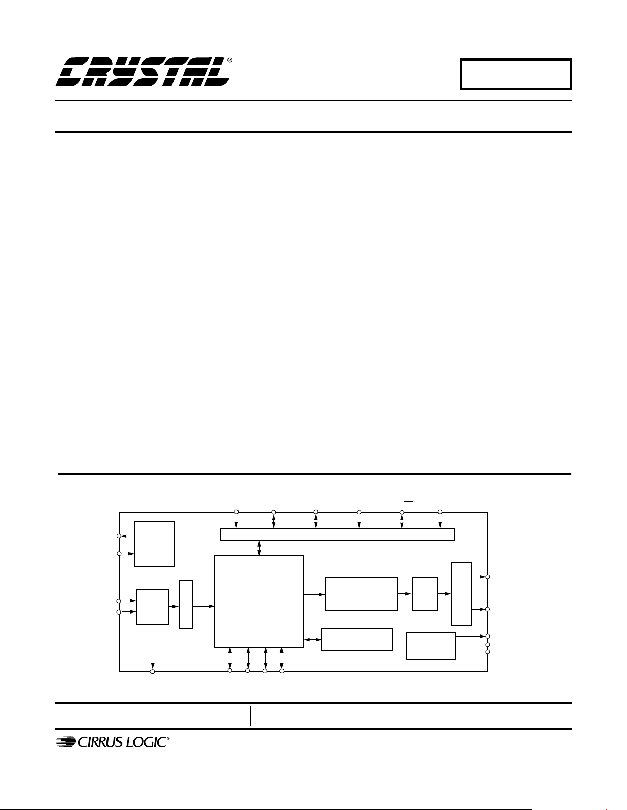
The CS4811 is a complete audio effects processing
system on a chip. This device integrates a proprietary 24bit audio processing engine, large on-chip RAM
memories, and a high performance 24-bit audio codec. A
serial control port allows the device to boot firmware from
a compact and low cost SPI or I
features such as single +5 V operation simplify system
design.
Firmware for the CS4811 is provided by Cirrus Logic.
There are two different firmware codes available; one for
guitar effects and one for audio mixers. The guitar effects
firmware provides a host of electric guitar effects including spring reverb, delay, chorus, flange and tremolo.
The mixer effects firmware provides a suite of effects
such as digital r everb, d elay and chorus which are suitable for use in audio mixers, karaoke and acoustic
instrument amplifiers. The CDB4811GTR and
CDB4811MXR evaluation boards allow easy evalua tion
of the CS4811 device and the associated firmware.
ORDERING INFO
CS4811-KM -10 to +70°C 100-pin MQFP
CDB4811GTR-01 Guitar Effects Evaluation Board
CDB4811MXR-01 Mixer Effects Evaluation Board
2
C serial EEPROM. Other
I
XTO
XTI
AIN+
AIN-
CLOCK
MANAGER
ADC
OVL
DIGITAL HPF
Advance Product Information
P.O. Box 17847, Austin, Texas 78760
(512) 445 7222 FAX: (512) 445 7581
http://www.cirrus.com
SPI/I2C
24-BIT AUDIO
PROCESSING
PIO0
SCL/CCLK
ENGINE
PIO1
PIO2
This document contains information for a new product.
Cirrus Logic reserves the right to modify this product without notice.
SDA/CDOUT
SERIAL CONTROL PORT (SPI or I2C)
PIO3
Copyright Cirrus Logic, Inc. 2000
AD1/CDIN
DIGITAL FILTER
RAM
(All Rights Reserved)
AD0/CS
RST
DAC
VOLTAGE
REFERENCE
OUTPUT STAGE
ANALOG LPF AND
AOUT+
AOUT-
CMOUT
CMFILT+
CMFILT-
SEP ‘00
DS486PP2
1
Page 2

TABLE OF CONTENTS
1. CHARACTERISTICS AND SPECIFICATIONS .................................. ....... ...... ....... ...... ....... ..... 4
ADC CHARACTERISTICS .......................................................................................................4
DAC CHARACTERISTICS .......................................................................................................5
SWITCHING CHARACTERISTICS ................................. ...... ....... ...... ....... ...... ....... ...... ............6
SWITCHING CHARACTERISTICS - CONTROL PORT - SPI MASTER..................................7
SWITCHING CHARACTERISTICS - CONTROL PORT - I
RECOMMENDED OPERATING CONDITIONS.......................................................................9
DIGITAL CHARACTERISTICS................................................................................................. 9
SWITCHING CHARACTERISTICS - PROGRAMMABLE I/O...................................................9
2. TYPICAL CONNECTION DIAGRAMS ................................................................................... 10
3. FUNCTIONAL DESCRIPTION ............................................................................................... 12
3.1 Overview ..........................................................................................................................12
3.2 Analog Inputs ...................................................................................................................12
3.2.1 Line Level Inputs ................................................................................................. 12
3.2.2 Digital High Pass Filter ........................................................................................12
3.3 Analog Outputs ................................................................................................................13
3.3.1 Line Level Outputs ..............................................................................................13
3.4 Clock Generation ............................................................................................................. 13
3.4.1 Clock Source .......................................................................................................13
3.5 Serial Control Port ............................................................................................................14
3.5.1 SPI Bus ...............................................................................................................14
3.5.1.1 SPI Mode ................................................................................................14
2
3.5.2 I
3.6 Resets ..............................................................................................................................15
4. POWER SUPPLY AND GROUNDING ................................................................................... 16
5. PIN DESCRIPTIONS ....................................................... ...... ............................................. . ... 17
6. PARAMETER DEFINITIONS ..................................................................................................21
7. PACKAGE DIMENSIONS ..................................................................................................... 22
C Bus ................................................................................................................14
3.5.2.1 I
CS4811
2
C MASTER......... ....... ...... ............8
2
C Mode ................................................................................................ 14
Contacting Cirrus Logic Support
For a complete listing of Direct Sales, Distributor, and Sales Representative contacts, visit the Cirrus Logic web site at:
http://www.cirrus.com/corporate/contacts/
Preliminary product inf o rmation describes products whi ch are in production, but f or which full characteriza t i on da t a i s not yet available. Advance produ ct i nformation describes products which are in development and subject to development changes. Cirrus Logic, Inc. has made best efforts to ensure that the information
contained in this document i s accurat e and reli able. However , t he infor mation is subje ct to chang e without noti ce and is provi d ed “AS IS” without warrant y of
any kind (express or implied). No responsibility is assumed by Cirrus Logic, Inc. for the use of this information, nor for infringements of patents or other ri g ht s
of third parties. This document is the pro perty of Cirrus Logi c, Inc. and i mplie s no licen se under patents, copyrights, tr ademarks, or trade secre ts. No part of
this publication may be copied, reproduced , stored in a retrieval system, or transmitted, in any form or by any means (electronic, mechanical, photographic, or
otherwise) without the pr i or writ ten consent of Cirrus Logic, Inc. Ite ms f rom any Ci rrus L ogi c websi t e or disk may be printed for use by the user. However, no
part of the printout or electronic files may be copied, reproduced, stored in a retrieval system, or transmitted, in any form or by any means (electronic, mechanical,
photographic, or otherwise) without the prior written consent of Cirrus Logic, Inc.Furthermore, no part of this publication may be used as a basis for manufacture
or sale of any items without the prior written consent of Cirrus Logic, Inc. The names of products of Cirrus Logic, Inc. or other vendors and suppliers appearing
in this document may be trademarks or service marks of their respective owners which may be registered in some jurisdictions. A list of Cirrus Logic, Inc. trademarks and service marks can be found at http://www.cirrus.com.
2 DS486PP2
Page 3

LIST OF FIGURES
CS4811
Figure 1. SPI Control Port Timing ............................................................................. 7
Figure 2. I
Figure 3. Typical Connection Diagram, Single-ended Input .................................... 10
Figure 4. Typical Connection Diagram, I
Figure 5. Typical Connection Diagram, SPI Mode .................................................. 11
Figure 6. Optional Line Input Buffer ........................................................................ 12
Figure 7. Butterworth Output Filters ........................................................................ 13
Figure 8. Output Mute Circuit .................................................................................. 13
Figure 9. Control Port Timing, SPI Master Mode Self-Boot ..................................... 14
Figure 10.Control Port Timing, I2C Master Mode Self-Boot ..................................... 15
Figure 11.CS4811 Suggested Layout ...................................................................... 16
Figure 12.Pin Assignments ...................................................................................... 17
2
C Control Port Timing .............................................................................. 8
2
C Mode .................................................. 11
DS486PP2 3
Page 4
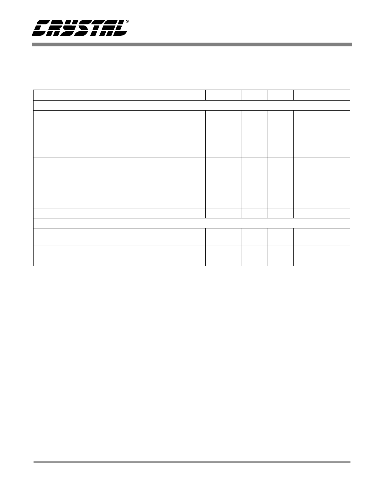
1. CHARACTERISTICS AND SPECIFICATIONS
CS4811
ADC CHARACTERISTICS (T
48 kHz; XTI = 12.2880 MHz; Measurement Bandwidth is 20 Hz to 20 kHz)
Parameters Symbol Min Typ Max Units
= 25° C; VA, VD = + 5 V; -1 dB Full Scale Input Sine wave, 997 Hz; Fs =
A
Analog Input Characteristics
ADC Conversion Stereo Audio channels 16 - 24 Bits
Dynamic Range (A weighted, Note 4)
(unweighted, Note 4)
Total Harmonic Distortion + Noise (Note 1,4) THD+N - -92 -87 dB
Offset Error (with internal high pass filter enabled) (Note 5) - - 0 LSB
Full Scale Input Voltage (Differential) 1.9 2.0 2.1 V
Gain Drift (Note 2) - 100 - ppm/°C
Input Resistance 10 - - kΩ
Input Capacitance - - 15 pF
CMOUT Output Voltage - 2.3 - V
Common Mode Rejection Ratio (Note 2) CMRR 60 dB
93
90
100
97
-
-
dB
dB
rms
High Pass Filter Characteristics
Frequency Response -3dB (Note 3)
-0.14dB (Note 3)
Phase Deviation @ 20 Hz (Note 3) - 10 - Degree
Passband Ripple - - 0 dB
-
-
3.7
20
-
-
Hz
Hz
Notes: 1. Referenced to typical full-scale differential input voltage (2 V
2. Bench tested only.
3. Filter characteristics scale with output sample rate.
4. Measured using differential analog input circuit, see Figure 6.
5. Filter response is not tested but is guaranteed by design.
rms
).
4 DS486PP2
Page 5
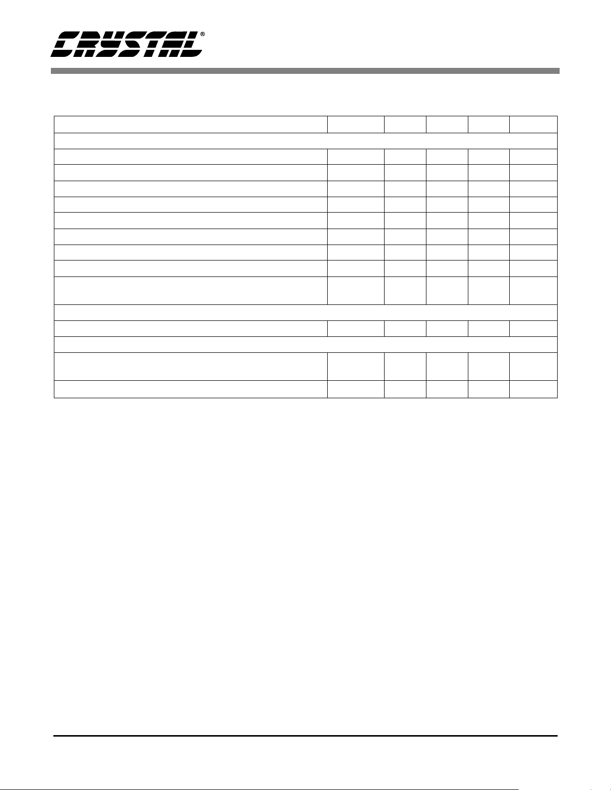
CS4811
DAC CHARACTERISTICS (T
48 kHz; XTI = 12.288 MHz; Measurement Bandwidth is 20 Hz to 20 kHz)
Parameters Symbol Min Typ Max Units
= 25° C; VA, VD = + 5 V; Full Scale Output Sine wave, 997 Hz; Fs =
A
Analog Output Characteristics - Minimum Attenuation, 10 kΩ, 100 pF load; unless otherwise specified.
DAC Resolution 16 - 24 Bits
Dynamic Range (DAC not muted, A weighted) 95 100 - dB
Total Harmonic Distortion + Noise THD+N - -90 -85 dB
Offset Voltage (differential) (Note 6) - -20±5 - mV
Offset Voltage (V+/V- relative to CMOUT) (Note 6) - -45/-28 - mV
Full Scale Output Voltage (Differential) 1.9 2.0 2.1 V
Gain Drift (Note 2) - 100 - ppm/°C
Out of Band Energy (Fs/2 to 2Fs, Note 2) - -60 - dBFS
Analog Output Load Resistance
Capacitance
10
-
-
-
-
100
rms
kΩ
pF
Analog Loopback Performance
Signal-to-Noise Ratio (CCIR-2K weighted, -20 dB input) CCIR-2K - 74 - dB
Power Supply
Power Supply Current Operating
Power Down (Note 7)
Power Supply Rejection (1 kHz, 10 mV
, Note 2) - 50 - dB
rms,
-
-
200
1
-
-
mA
mA
Notes: 6. Measured with DAC calibration disabled.
7. Measured with XTI clock disabled.
Specifications are subject to change without notice.
DS486PP2 5
Page 6
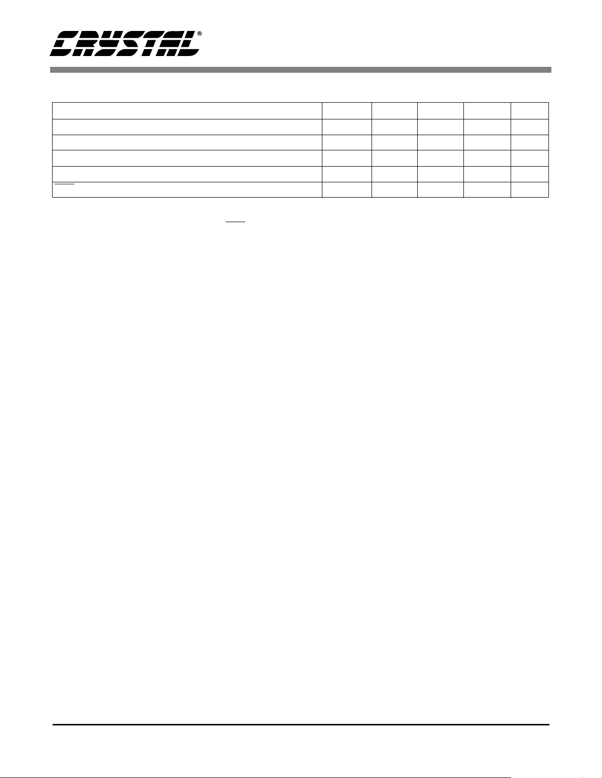
CS4811
SWITCHING CHARACTERISTICS (T
Parameters Symbol Min Typ Max Units
ADC & DAC Sample Rate Fs 30 - 50 kHz
XTI Frequency XTI = 256Fs 7.68 - 12.8 MHz
XTI Duty Cycle XTI =256Fs (Note 8) 40 - 60 %
XTI Jitter Tolerance - 500 - ps
RST
Low Time (Note 9) 500 - - ns
Notes: 8. Guaranteed by characterization but not tested.
9. On power-up, the CS4811 RST
state.
pin should be asserted until the power supplies have reached steady
= 25° C; VA, VD = +5 V, outputs loaded with 30 pF)
A
6 DS486PP2
Page 7
CS4811
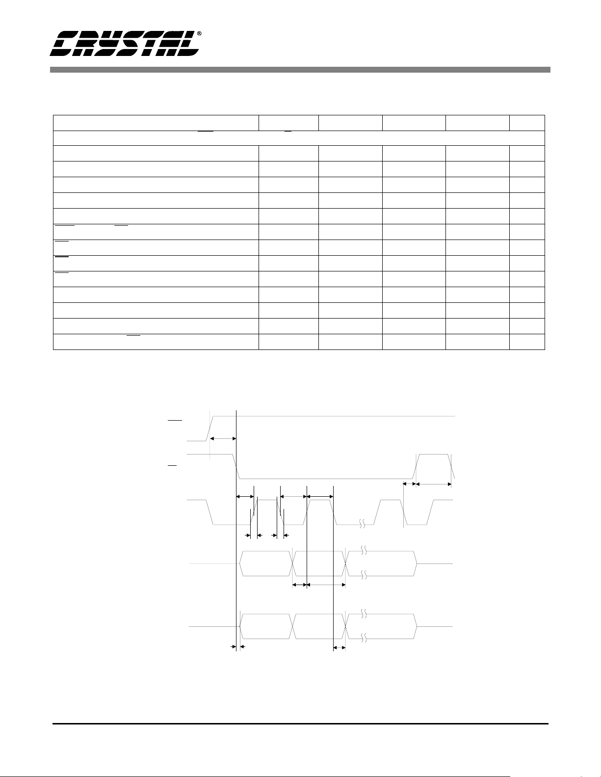
SWITCHING CHARACTERISTICS - CONTROL PORT - SPI MASTER (TA = 25° C,
VA, VD = 5 V; Inputs: lo gic 0 = DGND, logic 1 = VD, C
Parameter Symbol Min Typ Max Units
SPI Master (Self-Boot) Mode
(SPI/I2C = 0, SCPM/S = 1)
CCLK Clock Frequency
CCLK Low Time
CCLK High Time
CCLK Rise Time (Note 10)
CCLK Fall Time (Note 10)
rising to CS falling
RST
High Time Between Transmissions
CS
Falling to CCLK Edge
CS
Falling to CDOUT valid
CS
CCLK Falling to CDOUT valid
CDIN to CCLK Rising Setup Time
CCLK Rising to DATA Hold Time
CCLK Falling to CS
rising
= 30 pF)
L
f
sck
t
scl
t
sch
t
r2
t
f2
t
srs
t
csh
t
css
t
dv
t
pd
t
dsu
t
dh
t
clcs
-Fs-kHz
-1/(2*Fs)-ns
-1/(2*Fs)-ns
-12-ns
-12-ns
-42-µs
37 - - µs
5--µs
- - 50 ns
--100ns
80 - - ns
80 - - ns
40 - - ns
Notes: 10. Measured with a 2.2 kΩ pullup resistor to VD.
RST
CS
CCLK
CDIN
CDOUT
t
srs
t
css
t
scl
t
t
f2
dsu
t
r2
t
sch
t
dh
t
clcs
t
csh
t
dv
t
pd
Figure 1. SPI Control Port Timing
DS486PP2 7
Page 8
CS4811
SWITCHING CHARACTERISTICS - CONTROL PORT - I2C MASTER (T
VA, VD = 5 V; Inputs: lo gic 0 = DGND, logic 1 = VD, C
Parameter Symbol Min Typ Max Units
I2C® Master (Self-Boot) Mode
(SPI/I2C = 1, SCPM/S = 1) (Note 11)
SCL Clock Frequency
Clock Low Time
Clock High Time
Bus Free Time Between Transmissions
rising to start condition
RST
Start Condition Hold Time
Setup Time for Repeated Start Condition
SDA Setup Time to SCL Rising
SDA Hold Time from SCL Falling (Note 12)
SCL falling to SDA Output Valid
SCL and SDA Rise Time (Note 13)
SCL and SDA Fall Time (Note 13)
Setup Time for Stop Condition
Notes: 11. Use of the I
2
C bus interface requires a license from Philips. I2C is a registered trademark of Philips
Semiconductors.
12. Data must be held for sufficient time to bridge the worst case fall time of 300 ns for CCLK/SCL.
13. For both SDA transmitting and receiving.
= 30 pF)
L
f
scl
t
low
t
high
t
buf
t
irs
t
hdst
t
sust
t
sud
t
hdd
t
cldv
t
r
t
f
t
susp
-Fs-kHz
-1/(2*Fs)-µs
-1/(2*Fs)-µs
4.7 - - µs
-22-µs
4.0 - - µs
13.5 - - µs
250 - - ns
0--ns
--1.5µs
--1µs
--300ns
4.7 - - µs
= 25° C;
A
RST
t
SDA
SCL
(output)
irs
Stop Start
t
buf
t
hdst
t
low
t
cldv
t
hdd
t
high
t
sud
Repeated
Start
t
sust
t
hdst
Stop
t
f
t
r
t
susp
Figure 2. I2C Control Port Timing
8 DS486PP2
Page 9

CS4811
ABSOLUTE MAXIMUM RATINGS (All voltages with respect to AGND = DGND = 0 V.)
Parameters Symbol Min Typ Max Units
Power Supplies Digital
AnalogVDVA
Input Current (Note 14) - - ±10.0 mA
Analog Input Voltage (Note 15) -0.7 - (VA)+0.7 V
Digital Input Voltage (Note 15) -0.7 - (VD)+0.7 V
Ambient Temperature (Power Applied) -55 - +125 °C
Storage Temperature -65 - +150 °C
Notes: 14. Any pin except supplies. Transient currents of up to ±100 mA on the analog input pins will not cause
SCR latch-up.
15. The maximum over or under voltage is limited by the input current.
Warning: Operation at or beyond these limits may result in permanent damage to the device.
Normal operation is not guaranteed at these extremes.
-0.3
-0.3
-
-
6.0
6.0
V
V
RECOMMENDED OPERATING CONDITIONS (All voltages with respect to AGND = DGND =
0V.)
Parameters Symbol Min Typ Max Units
Power Supplies Digital
|VA - VD| < 0.4V AnalogVDVA
Operating Ambient Temperature T
DIGITAL CHARACTERISTICS (T
= 25° C; VA, VD = 5 V)
A
A
Parameters Symbol Min Typ Max Units
High-level Input Voltage (except XTI) V
Low-level Input Voltage (except XTI) V
High-level Output Voltage at I
Low-level Output Voltage at I
= -2.0 mA (except XTO) V
0
= 2.0 mA (except XTO) V
0
High-level Input Voltage (XTI) V
Low-level Input Voltage (XTI) V
IH
IL
OH
OL
IH
IL
Input Leakage Current (Digital Inputs) - - 10 µA
Output Leakage Current (High-Z Digital Outputs) - - 10 µA
SWITCHING CHARACTERISTICS - PROGRAMMABLE I/O (T
±5%; Inputs: logic 0 = DGND, logic 1 = VD, C
= 30 pF)
L
4.75
4.75
5.0
5.0
5.25
5.25
V
V
-10 25 70 °C
2.8 - (VD)+0.3 V
-0.3 - 0.8 V
(VD)-1.0 - - V
--0.4V
2.8 - - V
--2.3V
= 25° C; VA, VD = 5 V
A
Parameters Symbol Min Typ Max Units
Output Rise Time t
Output Fall Time t
rpo
fpo
-200-ns
-200-ns
DS486PP2 9
Page 10

2. TYPICAL CONNECTION DIAGRAMS
1µF 0.1µF
+
Ferrite Bead
1
+
µ
F 0.1µF
CS4811
+5 V Supply
22 µF
To Optional
Input and
Output Buffers
+
Serial EEPROM
+
100 µF
1 µF
150
1µF
AOUT
AOUT
RES-VD
RES-NC
RES-NC
RES-NC
DDA
7
+
-
ANALOG
8
FILTER
70, 73
9, 10, 14, 15, 16, 17, 20
21, 22, 23, 47, 57, 58, 59
60, 61, 71, 95, 97, 90, 91
VD
A
88
18
Ω
+
86
2.2 nF
A
0.1 µF
AA
39
12
VA 1..3
AIN
+
87
AIN-
OVL
4365
VD 1..2
CS4811
92
CMOUT
0.1 µF
AA
93
VD
94
2.2 K
63
62
68
67
CMFILT+
CMFILT-
SCL/CCLK
SDA/CDOUT
AD0/CS
AD1/CDIN
0.1 µF
A
VD
2.2 K
32, 36, 38, 48, 96, 82, 83
1, 2, 3, 4, 5, 6
24, 25, 26, 27, 28, 29, 30
31, 33, 49, 50, 51, 52, 53
54, 55, 56, 74, 75, 76, 77
78, 79, 80, 81, 84, 85, 98, 99, 100
D
Mode/Reset
Circuit
RESET
Control/
Monitor
Circuitry
R=33
S
All unused inputs
should be tied to ground.
Ω
RES-DGND
69
SPI/I2C
72
RST
41
PIO0
40
PIO1
37
PIO2
35
PIO3
AGND1..4 DGND1..4 XTO
13 8919
11
A
44
42
6664
D
46
39 pF
DD
XTI
45
1 M
39 pF
Ω
RES-DGND
RES-DGND
RES-DGND
RES-DGND
RES-DGND
Caps, Xtal, and
resistor not needed
with external clock
input to XTI.
Figure 3. Typical Connection Diagram, Single-ended Input
10 DS486PP2
Page 11

D
EEPROM
A0
A1
A2
2
IC
2.2 K
VD
VD
VD
D
2.2 K
63
62
68
67
69
CS4811
CS4811
SCL/CCLK
SDA/CDOUT
AD0/CS
AD1/CDIN
SPI/I2C
Reset
Circuit
RESET
72
RST
Figure 4. Typical Connection Diagram, I2C Mode
VD
VD
2.2 K
SPI
EEPROM
2.2 K
63
62
68
67
69
CS4811
SCL/CCLK
SDA/CDOUT
AD0/CS
AD1/CDIN
SPI/I2C
D
Reset
Circuit
RESET
72
RST
Figure 5. Typical Connection Diagram, SPI Mode
DS486PP2 11
Page 12

CS4811
3. FUNCTIONAL DESCRIPTION
3.1 Overview
The CS4811 is a complete audio subsystem on a
chip, integrating a proprietary 24-bit audio processing engine with large on chip RAM memories and
a single channel 24-bit audio codec.
The delta-sigma ADC includes linear phase digital
anti-aliasing filters and only requires a single-pole
external passive filter.
The sigma-delta DAC includes a switched-c apacitor anti-image filter and requires an external 2nd or
3rd order active filter that can be easily integrated
into the output differential-to-single-ended converter circuit.
The serial control port is designed to accommodate
I2C® or SPI interfaces for stand-alone operation
with an external non-volatile memory.
3.2 Analog Inputs
3.2.1 Line Level Inputs
AIN+ and AIN- are the differential l ine level analog inputs (See Figure 3). These pins are internally
biased to the CMOUT voltage of 2.3 V. A DC
blocking capacitor placed in series with the input
pins allows signals centered around 0 V to be input
to the CS4811. Figure 3 shows operation with a
single-ended input source. This source may be supplied to either the positive or negative input as long
as the unused input is connected to ground through
capacitors as shown. When operated with singleended inputs, distortion will increase at input levels
higher than -1 dB Full Scale. If better performance
is required, a single-ended-to-differential converter, shown in Figure 6, may be used. This circuit
provides unity gain, DC blocking on the input and
anti-alias filtering.
The OVL output pin asserts when the analog input
is out-of-range.
3.2.2 Digital High Pass Filter
In DC coupled systems, a small DC offset may exist between the input circuitry and the A/D converters. The CS4811 includes a high pass filter
after the decimator to remove these DC components. The high pass filter response, given in High
Pass Filter Characteristics, scales linearly with
sample rate. Thus, the -3 dB frequency at a
44.1 kHz sample rate will be equal to 44.1/48 times
that at a sample rate of 48 kHz.
4.7 k
10µF
10 k
Buffered
CMOUT
-
+
10 k
10 k
+5 V
+
+
µ
10
f
GND
0.1µF
input signal
(2 Vrms max)
CMOUT
from
CS4811
12 DS486PP2
+
-
+
Figure 6. Optional Line Input Buffer
150
AIN -
2.2 nf
150
AIN +
Page 13

CS4811
2-Pole Butterworth Filter
BUFFERED
CMOUT
_
+
Example
Op-Amp
s
are
MC33078
A
OU
T-
MUTE
Line
Out
14.0 k
Ω
14.0 k
Ω
A
OUT+
3.24 k
Ω
3.24 k
Ω
1000
pF
1000
pF
14.0 k
Ω
220 pF
220
pF
14.0 k
Ω
GND
+5 V
BUFFERED
CMOUT
_
+
MUTE
Line
Out
A
OUT+
A
OUT-
220
pF
220
pF
2200
pF
2.8k
Ω
2.8k
Ω
2.8k
Ω
2.8k
Ω
11.0k
Ω
11.0k
Ω
14.0k
Ω
14.0k
Ω
2200
pF
2200
pF
2200
pF
GND
+5 V
3-Pole Butterworth Filter
Figure 7. Butterworth Output Filters
3.3 Analog Outputs
3.3.1 Line Level Outputs
The CS4811 contains on-chip differential buffer
amplifiers that produce line level outputs AOUT+
and AOUT-, which are capable of driving 10 kΩ
loads. These amplifiers are internally biased to the
CMOUT voltage of 2.3 V.
The recommended off-chip analog filter is a 2nd
order Butterworth with a -3 dB corner at Fs. A third
order Butterworth filter with a -3 dB corner at
0.75 Fs can be used if greater out of band noise filtering is desired. These filters can be easily integrated into a differential-to-single-ended converter
circuit as shown in the 2-pole and 3-pole Butterworth filters of Figure 7. Figure 8 shows the rec-
ommended mute circuit referenced in Figure 7.
Activating the mute circuit is recommended on
power-up and power-down to avoid the output of
undesirable audio signals.
3.4 Clock Generation
The master clock to operate the CS4811 may be generated by using the on-chip oscillator with an external crystal or may be input from an external clock
source.
3.4.1 Clock Source
The CS4811 requires a 256 Fs master clock to run
the internal logic. The two possible clock sources
are the on-chip crystal oscillator or an external clock
input to the XTI pin.
The master clock may be generated directly from
the on-chip crystal oscillator circuit. When using
the on-chip crystal oscillator, external loading capacitors are required. (see Figure 3) High frequency crystals (>8 MHz) should be parallel resonant,
fundamental mode and designed for 20 pF loading.
(equivalent to 40 pF to ground on each leg)
The master clock may also be generated directly
from an external CMOS clock input to the XTI pin.
DS486PP2 13
VA
MMBT3906
From
CS4811
PIO
10 k
10 k
Ω
10 µF
Ω
1 kΩ10 µF
10 k
Ω
MMBT3906
3.3 k
+
MMBT3904
Ω
GND
Figure 8. Output Mute Circuit
Line Out
Page 14

CS4811
3.5 Serial Control Port
The serial control port is used for self-booting from
an external EEPROM and supports both the SPI
bus and the I2C® bus interfaces. The desired interface is selected via the SPI/I2C pin, which is sampled during de-assertion of the RST pin.
3.5.1 SPI Bus
The SPI bus interface consists of 4 digital signals,
CCLK, CDIN, CDOUT and CS. CCLK, the control
port bit clock, i s used to clock individual data bits.
CDIN, the control data input, is the serial data input
line to the CS4811. CDOUT, the control data output,
is the output data line from the CS4 811. CS, the chip
select signal, is asserted to enable an external SPI
port. Data is clocked in on the rising edge of CCLK
and clocked out on the falling edge.
3.5.1.1 SPI Mode
The
SPI
master mode is designed for read-only operation during self-booting from a serial EEPROM.
A typical self-boot sequence with a Xicor X25650 serial EEPROM, or equivalent, is shown in Figure 9. On
exit from reset, the CS4811 asserts CS. The 8-bit read
instruction (00000011) is sent to the EEPROM followed by a pre-defined 16-bit start address.
The
CS4811 then automatically clocks out sequential
bytes from the EEPROM until the last byte has
been received. These bytes include initialization
and configuration data for the device along with the
application firmware code.
After the last byte is received, the CS4811 deasse rts CS and begins program
execution. At this point, the serial control port becomes inactive and cannot be accessed.
3.5.2 I2C Bus
The I2C bus interface implemented on the CS4811
consists of 2 digital signals, SCL and SDA. SCL or
serial clock, is used to clock individual data bits.
SDA or serial data, is a bidirectional data line. Two
additional pins, AD1 and AD0, are inputs which
determine the 2 lowest order bits of the 7-bit I2C
device address and should be tied to ground.
3.5.2.1 I2C Mode
The I2C master mode is designed for read-only operation during self-booting from a serial EEPROM.
A typical self-boot sequence with a Microchip
X24256 serial EEPROM, or equivalent, is shown
in Figure 10. On exit from reset, the CS4811 sends
an initial write preamble to the EEPROM which
consists of a I2C start condition and the slave ad-
CS
0 1 2 21 22 23 24
CLK
CDIN
READ
COMMAND
CDOUT
MSB
Figure 9. Control Port Timing, SPI Master Mode Self-Bo ot
14 DS486PP2
7 8 9 10 113 4 5 6 3 0 3125 26 27 28 29
DATA
7 6 5 4 3 2 1 0
16-BIT
ADDRESS = 0X0000
0 0 0 0 0 0 00 0 0 0 0 0 1 1
DATA + n
7 6 5 4 3 2 1 0
Page 15

CS4811
dress byte. The slave address consists of the 4 most
significant bits set to 1010, the following 3 bits corresponding to the device select bits, A2, A1 and A0
set to 000 and the last bit (R/W) set to 0. Following
this, a 2-byte EEPROM starting address of 0x0000
is sent to the EEPROM. The 2-byte EEPROM
starting address uses only the lowest 13 bits and
sets the highest 3 bits to zero. To begin reading
from the EEPROM, the CS4811 sends another start
condition followed by a read preamble. The read
preamble is identical to the write preamble except
for the state of the R/W bit. The CS4811 then automatically clocks out sequential bytes from the EEPROM until the last byte has been received. These
bytes include initialization and configuration data
for the device along with the application firmware
code. After the last byte, the CS4811 initiates a stop
condition and begins program execution. At this
point, the serial control port becomes inactive and
cannot be accessed.
3.6 Resets
Full chip reset can only be achieved by asserting
the RST pin. With RST asserted, the chip enters
low power mode during which the control port,
CODEC and Audio Processor are reset, all registers
are returned to their default values and the DAC
outputs are muted. The RST pin should be asserted
during power-up until the power supplies have
reached steady state.
If the supply voltage drops below 4 Volts, the CODEC is reset, the DAC outputs are muted and the
Audio Processor automatically executes a soft reset.
Upon exit from a CODEC reset, the Audio Processor restarts the application code and the CODEC
performs the following procedure:
• The CODEC resynchronizes.
• The DAC outputs unmute.
SCL
SDA
0 1 2 3
CHIP ADDRESS (WRITE) CHIP ADDRESS (READ)MEMORY ADDRESS DATA DATA +n
1 0 1 0 A2 A1 A0 0 0 0 0 0 0 0 1 0 1 0 A2 A1 A0 1
START
4 5 6 7
ACK NO
Figure 10. Control Port Timing, I2C Master Mode Self-Boot
16 17 18 19 25 26 27 28 29
ACK
START STOP
34 35 36 3730 31 32 338 9 10
7 0
ACKACK
7 0
ACK
DS486PP2 15
Page 16

CS4811
4. POWER SUPPLY AND GROUNDING
Proper layout and grounding is critical to obtaining
optimal audio performance in your system. The
most important rule to remember is to not allow
currents from digital circuitry to couple into sensitive analog circuitry. This is generally done by using a separate or filtered power supply for the
analog circuitry, physically separating the analog
and digital components and traces in the pcb layout
and using wide traces or planes for ground and
power. One misplaced component or trace can severely degrade overall system performance.
When using separate supplies, the analog and digital power should be connected via a ferrite bead,
positioned closer than 1" to the device (see
Figure 11). The CS4811 VA pin should be derived
from the quietest power source available. If only
one supply is available, use the suggested arrangement in Figure 3.
Figure 3 are tied to the same ground plane. However, if separate analog and digital grounds are used,
they should be tied together at one point with the
location of this point determined by the circuit layout. By considering where the digital ground currents will return to their supply, the connection
point can be chosen to keep those currents from
flowing through sensitive analog circuit areas.
Decoupling capacitors should be placed as close as
possible to the device with the lowest value capacitor closest to the chip. Any power and ground connection vias should be placed near their respective
component pins and should be attached directly to
the appropriate plane. If traces are used for the
power supplies to the CS4811, they should be as
wide as possible to maintain low impedance.
It is recommended to solder the CS4811 directly to
the printed circuit board. Soldering improves performance and enhances reliability.
A single solid ground plane is the simplest grounding scheme that works well in many cases. In this
case, all analog and digital grounds shown in
>
1/8"
Digital
Power
Plane
Digital Interface
For an example layout, please refer to the
CDB4811 data sheet.
Ferrite
Bead
CS4811
Analog Signals &
Components
Analog
Power
Plane
Note that the CS4811
is oriented with its
digital pins towards the
digital end of the board.
Figure 11. CS 4811 Suggested Layout
16 DS486PP2
Page 17

5. PIN DESCRIPTIONS
CS4811
DGND
AD1/CDIN
AD0/CS
SPI/I2C
RES-VD
RES-NC
RST
RES-VD
NC
NC
NC
NC
NC
NC
NC
NC
RES-DGND
RES-DGND
NC
NC
AIN+
AIN-
VA
AGND
RES-NC
RES-NC
CMOUT
CMFILT+
CMFILT-
RES-NC
RES-DGND
RES-NC
NC
NC
NC
NC
NC
NC
NC
NC
NC
AOUT+
AOUTRES-NC
RES-NC
AGND
VA
AGND
RES-NC
RES-NC
80 79 78 77 76 75 74 73 72 71 70 69 6867 66 65 64 63 62 61 60 59 58 57 56 55 54 53 52 51
80 79 78 77 76 75 74 73 72 71 70 69 6867 66 65 64 63 62 61 60 59 58 57 56 55 54 53 52 51
81
81
82
82
83
83
84
84
85
85
86
86
87
87
88
88
89
89
90
90
91
91
92
92
93
93
94
94
95
95
96
96
97
97
98
98
99
99
100
100
1 2 3 4 5 6 7 8 9 10 11 12 13 14 15 16 17 18 19 20 21 22 2324 25 26 27 28 29 30
1 2 3 4 5 6 7 8 9 10 11 12 13 14 15 16 17 18 19 20 21 22 2324 25 26 27 28 29 30
CS4811
CS4811
100-PIN MQFP
100-PIN MQFP
VD
VD
DGND
DGND
SCL/CCLK
SCL/CCLK
SDA/CDOUT
SDA/CDOUT
RES-NC
RES-NC
RES-NC
RES-NC
RES-NC
RES-NC
RES-NC
RES-NC
RES-NC
RES-NC
NC
NC
NC
NC
NC
NC
NC
NC
NC
NC
NC
NC
NC
NC
NC
NC
RES-DGND
RES-DGND
RES-NC
50
50
49
49
48
48
47
47
46
46
45
45
44
44
43
43
42
42
41
41
40
40
39
39
38
38
37
37
36
36
35
35
34
34
33
33
32
32
31
31
RES-NC
XTO
XTO
XTI
XTI
DGND
DGND
VD
VD
DGND
DGND
PIO0
PIO0
PIO1
PIO1
OVL
OVL
RES-DGND
RES-DGND
PIO2
PIO2
RES-DGND
RES-DGND
PIO3
PIO3
RES-DGND
RES-DGND
NC
NC
RES-DGND
RES-DGND
NC
NC
NC
NC
NC
NC
NC
NC
NC
NC
NC
NC
NC
NC
NC
NC
RES-NC
RES-NC
RES-NC
RES-NC
RES-NC
RES-NC
RES-NC
RES-NC
AGND
AGND
VA
VA
RES-NC
RES-NC
RES-NC
RES-NC
Figure 12. Pin Assignments
DS486PP2 17
Page 18

Power Supply
VA - Analog Power
Power:
AGND - Analog Ground
Ground:
VD - Digital Power
Power:
DGND - Digital Ground
Ground:
Analog Input
AIN+/- - Differential Audi o Input
Inputs:
voltage of approximately 2.3 V. The + and - input signals should be 180° out of phase resulting in a
nominal differential input voltage of twice the input pin voltage. A single-ended signal may also be
directly applied to eit her the + or - input with the othe r input AC coupled to ground th rough a capacitor.
In general, differential input signals provide better performance. However, singled-ended inputs may
result in reduce d cost. Inputs may be AC or D C coupled. DC coupled input s ignals must be biased at
2.3 V. Any remaining DC offset is removed by an internal digital HPF. For best perf ormance, a passive
anti-aliasing filter is required. The typical connection diagram in Figure 3. shows the recommended
single-ended inp ut circuit. Figure 6 shows the recomm ended differen tial input circuit.
analog supply, +5 V.
analog ground.
digital supply, +5 V.
digital ground.
These pins accept differential analog input signals and are biased to the internal reference
CS4811
OVL - ADC Overload Indic ator
Output:
clipping stops.
Analog Output
AOUT+/- - Differential Audio Output
Outputs:
of approximately 2.3 V. The + and - output signals are 180° out of phase resulting in a nominal
differential output volt age of twice the output pin voltage. For best perfo rmance, an anti-imaging filter is
required. Figure 7 shows the recommended second and third order Butterworth differential-to-singleended output buffe r circuits.
This pin is asserted when the ADC is clipping. The pin does not latch and de-asserts when
These pins output differential analo g signals which are biased to the inte rnal reference voltage
18 DS486PP2
Page 19

Voltage Reference
CMOUT - Common Mode Output
Output:
analog circuitry. The load on CMOUT must be DC only, with an impedance of not less than 50 kilohms.
CMFILT+,CMFILT- - Common Mode Filter Connections
Inputs:
reference circuit. See the typical connection di agram in Figure 3. for details.
Serial Control Port
SPI
/I2C - Serial Control Po rt Format Select
Input:
SCL/CCLK - Serial Control Port Clock
Output:
control port data into CDIN and out o f CDOUT.
AD0/CS - I2C Address Bit 0 / SPI Chip Select
Input/Output:
and is used to select the boot EEPROM.
This pin provides an internally generated reference of 2.3 V to be used for biasing external
These pins are connec tions for extern al filter compone nts required by the in ternal common mod e
This pin configures the co ntrol port for I2C format if tied to VD or SPI format if tied to DGND.
This pin clocks ser ial control port data into and ou t of SDA in I2C mode. In SPI mode, it clocks
In I2C® mode, AD0 is an i nput and must be tied to gro und. In SPI mode, CS is an output
CS4811
AD1/CDIN - I2C Address Bit 1 / SPI Data Input
Input:
In I2C® mode, AD1 is an input and must be tied to ground. In SPI mode, CDIN is the serial
control port data input an d is clocked in on the r ising edge of CCLK.
SDA/CDOUT - I2C Data / SPI Data Output
Bidirectional/ Output:
serial control port data outpu t and is clocked out on the fal ling edge of CCLK.
Clock and Crystal
XTI, XTO - Crystal Oscillator Connec tions (Master Clock)
Input, Output:
Alternately, an external clock source may be applied to XTI. The clock frequen cy must be 256xFs.
In I2C® mode, SDA is the bidirectional data I/O line. In SPI mode, CDOUT is the
These pins provide connections for an external parallel resonant quartz crystal.
DS486PP2 19
Page 20

Miscellaneous
PIO0:3 - General Purpose I nputs/Outputs
Bidirectional:
functionality of these pins after boot-up is determi ned by the applicatio n firmware.
RST - Reset
Input:
This pin causes the de vice to enter a low power mode and forces all c ontrol port and I/O registers
to be reset to their default val ues. The control port can n ot be accessed when rese t is low.
NC - No Connect
Input:
These pins are not internal ly connected and should be tied to ground for optim al performance.
RES-NC - Reserved, No Connect
These pins are reserved and m ust be left unconnected for normal operatio n.
RES-VD - Reserved, Connect to VD
These pins are reserved and m ust be tied to VD for norma l operation.
RES-DGND - Reserved, Connect to DGND
These pins are reserved and m ust be tied to digital ground for normal operation.
These pins are general-purpose digital I/O pins. The Default state is input. The
CS4811
RES-AGND - Reserved, Connect to AGND
These pins are reserved and m ust be tied to analog grou nd for normal operation .
20 DS486PP2
Page 21

6. PARAMETER DEFINITIONS
Dynamic Range
The ratio of the full scale RMS value of the signal to the RMS sum of all other spectral components
over the specified bandwidth. Dynamic range is a signal-to-noise measurement over the specified
bandwidth made with a -60 dbFs signal. 60 dB is then ad ded to the resulting measurement to refer the
measurement to full scale. This technique ensures that the distortion components are below the noise
level and do not effect the measurement. This meas urement technique has be en accepted by the Audi o
Engineering Society, AES17-1991, and the Electronic Indus tries Associatio n of Japan, EIAJ CP-307.
Total Harmonic Distortion + Noise
The ratio of the RMS value of the signal to the RMS sum of all other spectral components over the
specified bandwidth (ty pically 20 Hz to 20 kHz), including distorti on components. Expressed in decibe ls.
ADCs are measured at -1 dB Fs as suggested in AES 17-1991 Anne x A.
Idle Channel Noise / Signal-to-Noise-Ratio
The ratio of the RMS analog output level with 1 kHz full scale digital input to the RMS analog output
level with all ze ros into the digital input. M easured A-weighted over a 10 Hz to 20 kHz bandwidth. Units
in decibels. This specification has been standardized by the Audio Engineering Society, AES17-1991,
and referred to as Idle Channel No ise. This specification has also been standardized by the Electronic
Industries Associati on of Japan, EIAJ CP-307, an d referred to as Signal -to-Noise-Ratio.
Total Harmonic Distortion (THD)
THD is the ratio of the test signal amplitude to the RMS sum of all the in-band harmonics of the test
signal. Units in decibe ls.
Interchannel Isolation
A measure of cro sstalk between channels. Me asured for each channe l at the converter’s output with no
signal to the input unde r test and a full-sca le signal appli ed to the other channe l. Units in decibels.
CS4811
Frequency Response
A measure of the a mplitude response variatio n from 20 Hz to 20 kHz relativ e to the amplitude respo nse
at 1 kHz. Units in decibels.
Interchannel Gain Mismatch
For the ADCs, the difference in input voltage that generates the full scale code for each channel. For
the DACs, the differenc e in output voltages for each channel with a full scale d igital input. Units are in
decibels.
Gain Error
The deviation from the nomi nal full scale output fo r a full scale input.
Gain Drift
The change in gain value with temperature. Units in ppm/ °C.
Offset Error
For the ADCs, the deviation in LSB's of the out put from mid-scale with the selecte d input grounded. For
the DAC's, the deviation of the output from zero (relative to CMOUT) with mid-scale input code. Units
are in volts.
DS486PP2 21
Page 22

7. PACKAGE DIMENSIONS
100L MQFP PACKAGE DRAWING
D1
D
CS4811
E
E1
1
e
B
∝
A1
L
INCHES MILLIMETERS
DIM M IN NOM MAX MIN NOM MAX
A -- -- 0.134 -- -- 3.400
A1 0.010 0.012 0.014 0.250 0.30 0.350
B 0.009 0.012 0.015 0.220 0.30 0.380
D 0.667 0.677 0.687 16.950 17.20 17.450
D1 0.547 0.551 0.555 13.900 14.00 14.100
E 0.904 0.91 0.923 22.950 23.20 23.450
E1 0.783 0.79 0.791 19.900 20.0 20.100
e* 0.022 0.026 0.030 0.550 0.65 0.750
∝
L 0.029 0.035 0.041 0.73 0.88 1.03
* Nominal pin pitch is 0.65 mm = 0.65 BSC
0.000° 4.00° 7.000° 0.00° 4.00° 7.00°
A
Controlling dimension is mm.
JEDEC Designation: MS022
ASE/SPIL
22 DS486PP2
Page 23

• Notes •
Page 24

 Loading...