

CS4610/11
Advanced Product Databook
FEATURES
■ High Performance PCI Audio Accelerator
— Powerful RAM-based SLIMD™ DSP core provides high
task concurrency and maximum flexibility
— Efficient bus mastering PCI interface minimizes host
loading
— DMA engine with hardware scatter-gather manages up
to 96 simultaneous audio/data streams
■ Flexible Digital Audio Interface Design
— Direct Connection to CS423x Codec
— Simple expansion to 6 audio output channels
— Direct Connection to CS4297 AC’97 Codec
■ Complete Solution including DSP Software and
Windows 95
— Acceleration of DirectSound®, DirectSound3D®, Direct-
Input™, and DirectS how™ APIs
— High Quality HRTF-Based 3D Positional Sound
— General MIDI Wavetable Synthesis with Reverb and
Chorus
—Dolby® AC-3® (5.1 channel) and MPEG-2 Audio Decod-
ing (CS4610 only) with speaker virtualization
®
drivers
DESCRIPTION
The CS4610/11 is a high performance audio accelerator for the PCI bus. This device, combined with
application and driver software, provides a complete system solution for hardware acceleration of
Windows 95 DirectSound, DirectSound3D, DirectInput, DirectShow, and Wavetable Synthesis.
CrystalClear™
SoundFusion™ PC I Audio
Accelerator
The CS4610/11 is based on t he Cirrus Logi c, CrystalClear Stream Processor (SP) DSP c ore. The SP
core is optimized for digital audio processing, and
is powerful enough to handle complex signal processing tasks such as Dolby AC-3 decoding
(CS4610 only) with ease. The S P core is supported
by a bus mastering PCI in terface and a built-in dedicated DMA engine with hardware scatter-gather
support. These support functions ensure extremely
efficient transfer of audio data streams to and from
host-based memory buffers, providing a system
solution with maximum performance and minimal
host CPU loading.
The all-digital CS4610/11 supports a variety of audio I/O configurations, including direct connection
to the CrystalClear CS423x Codecs via a bi-directional serial data link, or direct connection to an
AC’97 Codec such as the CrystalClear CS4297.
ORDERING INFORMATION
CS4610-CM 100-pin MQFP 20x14x3.07 mm
CS4610C-CQ 128-pin TQFP 20x14x1.60 mm
CS4611-CM 100-pin MQFP 20x14x3.07 mm
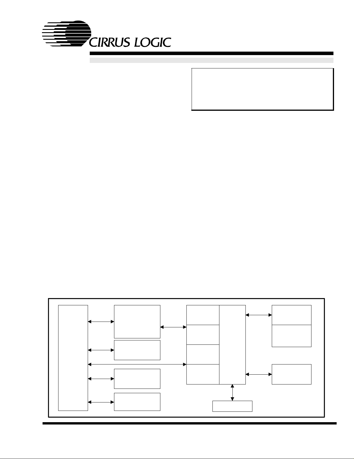
96-Stream
DMA Controll er
with Hardware
Scatter/Gather
Interrupt
PCI
Controller
Interface
MPU-401
MIDI Interface
Joystick
Interface
DS241PP5 MAR ‘98
Copyright Cirrus Logic, Inc. 1998
(All Rights Reserved)
Parameter
RAM
Program
RAM
Sample
RAM
Coefficient
ROM
SLIMD
SP Core
GPIO
AC ’97
Interface
423x Interface
and Dual I S
Output
PLL Clock
Generator
2
CS4610/11
CrystalClear™ SoundFusion™ PCI Audio Accelerator
ABSOLUTE MAXIMUM RATINGS
(PCIGND = CGND = CRYGND = 0 V, all voltages with respect to 0 V)
Parameter Symbol Min Typ Max Unit
Power Supplies PCIVDD
CVDD
CRYVDD
VDD5REF
Total Power Dissipation (Note 1) - - 1.5 W
Input Current per Pin, DC (Except suppl y pins) - - 10 mA
Output current per pin, DC - - 10 mA
Input voltage (Note 2) -0.3 - 5.75 V
Ambient temperature (power applied) (Note 3) -45 - 85 °C
Stor age temperature -55 - 150 °C
Notes: 1. Includes all power generated by AC and/or DC output loading.
2. The power supply pins are at reco mmende d maximum valu es. XTALI & XTALO are at 3.6 V maximum.
3. At ambient temperatures above 70° C, total power dissipation must be limited to less than 0.4 Watts.
-
-
-
-
-
-
-
-
4.6
4.6
4.6
5.5
V
V
V
V
WARNING: Operation beyond these limits may result in permanent damage to the device.
Normal operation is not guaranteed at these extremes.
RECOMMENDED OPERATING CONDITIONS
(PCIGND = CGND = CRYGND = 0 V, all voltages with respect to 0 V)
Min Typ Max Min Typ Max
Parameter Symbol
Power Supplies PCIVDD
CVDD
CRYVDD
VDD5REF
Internal DSP Frequency - - 100 - - 85 MHz
Operating Ambient Temperature T
Dolby’s AC3 Technology is implemented on the CS4610 Stream Processor Only. Supply of this Implementation of Dolby
Technology does not convey a license nor imply a right under any patent, or any other Industrial or Intellectual Property
Right of Dolby Laboratories, to use this Implementation in any finished end-user or ready-to-use final product. It is hereby
notified that a license for such use is required from Dolby Laboratories.
Specifications are subject to change without notice.
A
3
3
3
4.75
0257002570°C
3.3
3.3
3.3
5
3.6
3.6
3.6
5.25
3
3
3
4.75
3.3
3.3
3.3
5
3.6
3.6
3.6
5.25
UnitCS4610 CS461 1
V
V
V
V
Dolby and AC-3 are registered trademarks of Dolby Laboratories Licensing Corporation.
Windows, Windows 95, DirectSound, and DirectSound3D are registered trademarks of Microsoft Corporation.
DirectInput, DirectX and DirectShow are trademarks of Microsoft Corporation.
Sound Blaster and Sound Blaster Pro are trademarks of Creative Technology, Ltd.
Crystal, CrystalClear, SLIMD and SoundFusion are trademarks of Cirrus Logic, Inc.
All other names are trademarks, registered trademarks, or service marks of their respective companies.
2 DS241PP5
CS4610/11
CrystalClear™ SoundFusion™ PCI Audio Accelerator
AC CHARACTERISTICS (PCI SIGNAL PINS ONLY) (T
= 70° C;
A
PCIVDD = CVDD = CRYVDD = 3.3 V; VDD5REF = 5 V; PCIGND = CGND = CRYGND = 0 V;
Logic 0 = 0 V, Logic 1 = 3.3 V; Reference levels = 1.4 V; unless otherwise noted; (Note 4))
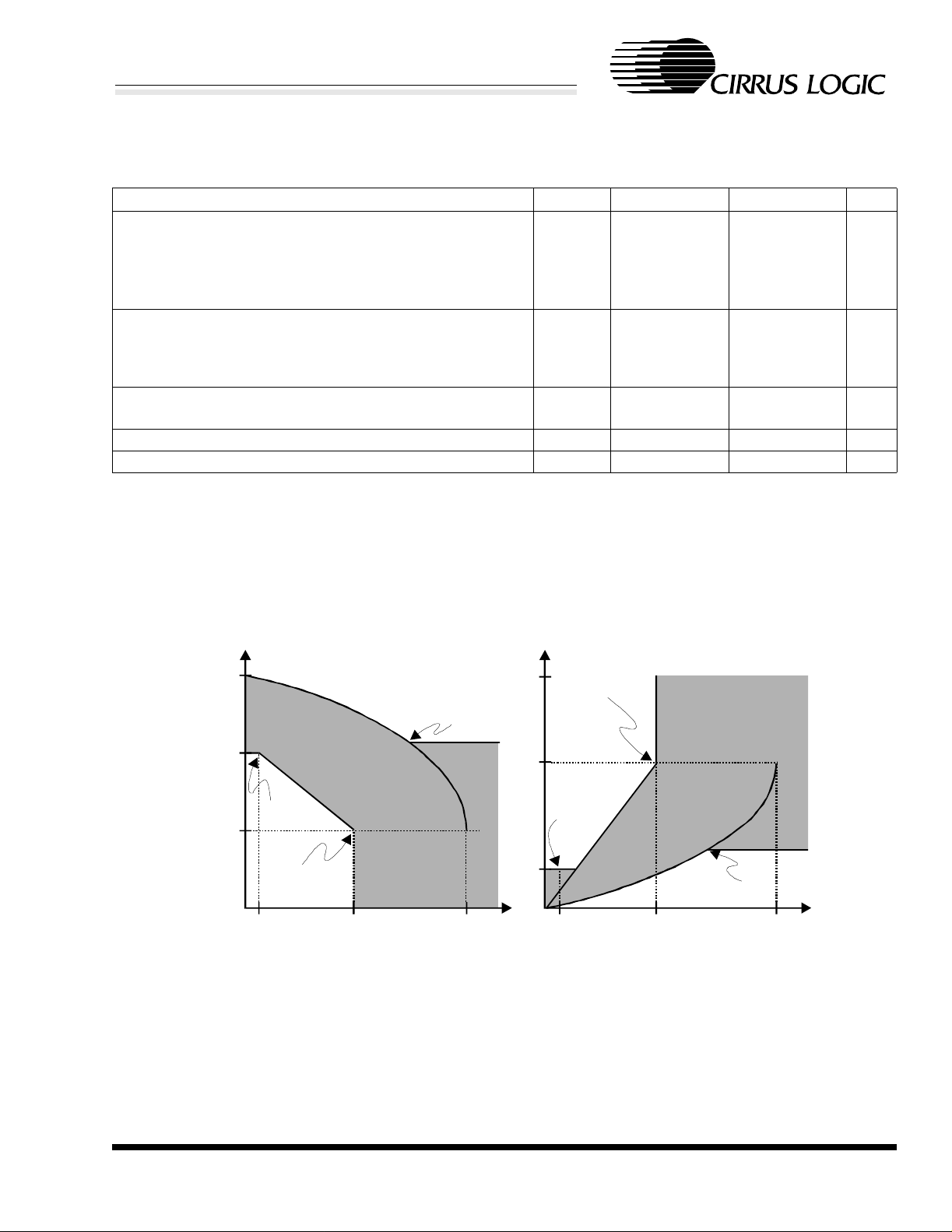
Parameter Symbol Min Max Unit
Switching Current High (Note 5)
0 < Vout < 1.4
1.4 < Vout < 2.4
3.1 < Vout < 3.3
Switching Current Low (Note 5)
Vout > 2.2
2.2 > Vout > 0.55
0.71 > Vout > 0
Low Clamp Current -5 < Vin < -1 I
I
I
OH
OL
CL
-44
Vout
44–
---------------------------+
0.024
-
95
Vout /0.023
-
Vin
25–
-------------------+
0.015
-
1.4–
-
mA
mA
Note 7
-
-
mA
mA
Note 8
1+
-mA
Output rise slew rate 0.4 V - 2.4 V load (Note 6) slewr 1 5 V/ns
Output fall slew rate 2.4 V - 0.4 V load (Note 6) slewf 1 5 V/ns
Notes: 4. Specifications guaranteed by characterization and not production testing.
5. Refer to V/I curves in Figure 1. Specification does not apply to CLK and RST# signals. Switching Current
High specification does not apply to SERR# and INTA# which are open drain outputs.
6. Cumulative edge rate across specified range. Rise slew rates do not apply to open drai n outputs.
7. Equation A: I
8. Equation B: I
= 11.9 * (Vout - 5.25) * (Vout + 2.4 5 ) for 3.3 V > Vout > 3.1 V
OH
= 78.5 * Vout * (4.4 - Vout) for 0 V < Vout < 0.71 V
OL
AC drive
point
Pull U p
-
3.3
test
point
2.2
0.55
Current (mA) Curre nt (mA)
44
-
176
voltage voltage
3.3
2.4
DC
1.4
drive point
-2
I = 11.9*(Vout-5.25)*(Vout+2.45)
OH
for 3.3V > Vout > 3.1 V
Figure 1. AC Characteristics
Pull Down
AC drive
point
DC drive
point
test
point
3, 6 95 380
Equation B:Equation A:
I = 78.5*Vout*(4.4-Vout)
OL
for 0V < Vout< 0.71V
DS241PP5 3
CS4610/11
CrystalClear™ SoundFusion™ PCI Audio Accelerator
DC CHARACTERISTICS (T
= 70° C; PCIVDD = CVDD = CRYVDD = 3.3 V; VDD5REF = 5 V;
A
PCIGND = CGND = CRYGND = 0 V; all voltages with respect to 0 V unless otherwise noted)
Parameter Symbol Min Typ Max Unit
PCI Inte rf a ce S ig n a l P in s
High level input volta ge V
Low level input vol tage V
High level output voltage Iout = -2 mA V
Low level output voltage Iout = 3 mA, 6 mA (Note 9) V
High level leakage current Vin = 2.7 V (Note 10) I
Low level leakage current Vin = 0.5 V (Note 10) I
IH
IL
OH
OL
IH
IL
2-5.75V
-0.5 - 0.8 V
2.4 - - V
--0.55V
--70µA
---70µA
Non-PCI Interface Signal Pins (Except XTALO)
High level input volta ge XTALI
Other Pins
Low level input vol tage XTALI
Other Pins
High level output voltage Iout = -4 mA (Note 11) V
Low level output voltage Iout = 4 mA V
High level leakage current Vin = 5.25 V I
Low level leakage current Vin = 0 I
V
IH
V
IL
OH
OL
IH
IL
2.3
2
-0.5
-0.5
3.3
-
0
-
2.4 - - V
--0.4V
--10µA
---10µA
4.0
5.75
0.8
0.8
V
V
V
V
Min Typ Max Min Typ Max
Parameter
UnitCS4610 CS4611
Power Supply Pins (Outputs Unloaded)
Power Supply Current: VDD5REF
PCIVDD/CVDD/CRYVDD Total (Notes 4,12)
-
-
0.6
200
-
370
-
-
0.6
164
-
240
mA
mA
Low Power Mode Supply Current - 10 - - 10 - mA
Notes: 9. The following signals are tested to 6 mA: FRAME#, TRDY#, IRDY#, DEVSEL#, STOP#, SERR#,
PERR#, and INTA#. All other PCI interface signals are tested to 3 mA.
10. Input leakage currents incl ude hi-Z outp ut l eakage f or al l bi -dire cti onal buf fers wit h th ree-st ate outp uts.
At supply voltages of 3.6 V or higher and amb ient temperatures of 70° C, the high level leakage current
may exceed 70 µA. For normal operating ranges of 25° C and a supply voltage of 3.3 V, t he high level
leakage current is within specification.
11. For open drain pins, high level output voltage is dependent on external pull-up used and number of
attached gates.
12. Typical values are given as average curr ent with t ypical SP task execution and data st reaming. Cur rent
values vary dramatically based on the software running on the SP.
4 DS241PP5
CS4610/11
CrystalClear™ SoundFusion™ PCI Audio Accelerator
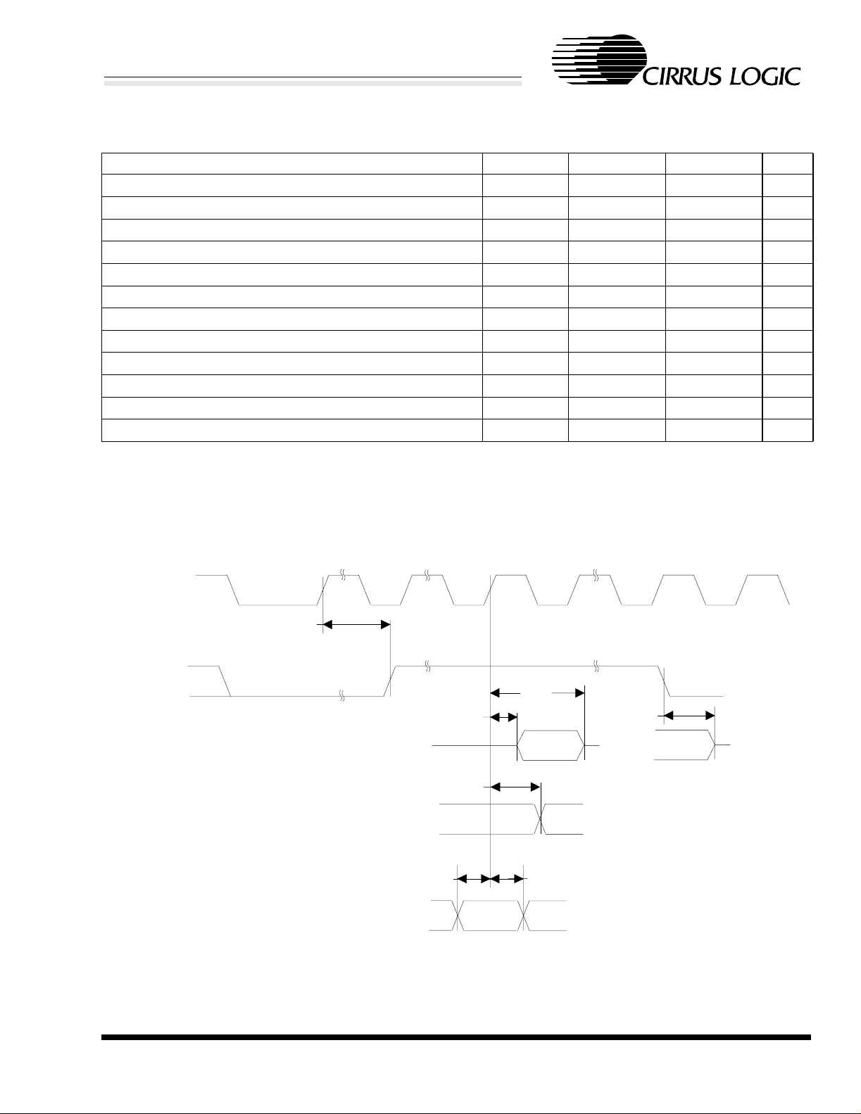
PCI INTERFACE PINS (T
PCIGND = CGND = CRYGND = 0 V; Logic 0 = 0 V, Logic 1 = 3.3 V; Timing reference levels = 1.4 V)
Parameter Symbol Min Max Unit
PCICLK cycle time t
PCICLK high time t
PCICLK low time t
PCICLK to signal valid delay - bused signals t
PCICLK to signal valid delay - point to point t
Float to active delay (Note 13) t
Active to Float delay (Note 13) t
Input Set up Time to PCICLK - bused signals t
Input Set up Time to PCICLK - point to point t
Input hold time for PCICLK t
Reset active time after PCICLK st able (Note 14) t
Reset active to output float delay (Notes 13, 14, 15) t
Notes: 13. For Active/Float measureme nts, t he Hi-Z or “of f” st ate i s whe n the t otal curren t deliver ed is l ess tha n or
equal to the leakage current . Specification is guarant eed by design, not production tested.
14. RST# is asserted and de-asserted asynchronously with re spect to PCICLK.
15. All output drivers are asynchronously floated when RST# is active.
= 0 to 70° C; PCIVDD = CVDD = CRYVDD = 3.3 V; VDD5REF = 5 V;
A
cyc
high
low
val
val(p+p)
on
off
su
su(p+p)
h
rst-clk
rst-off
30 - ns
11 - ns
11 - ns
211ns
212ns
2-ns
-28ns
7-ns
10, 12 - ns
0-ns
100 -
-40ns
µ
s
PCICLK
RST#
t
rst-clk
t
off
t
on
OUTPUTS
Hi-Z
t
val
OUTPUTS
Valid
t
su
INPUTS
Figure 2. PCI Timing Measurement Conditions
Valid
Input
t
h
t
rst-off
DS241PP5 5
CS4610/11
CrystalClear™ SoundFusion™ PCI Audio Accelerator
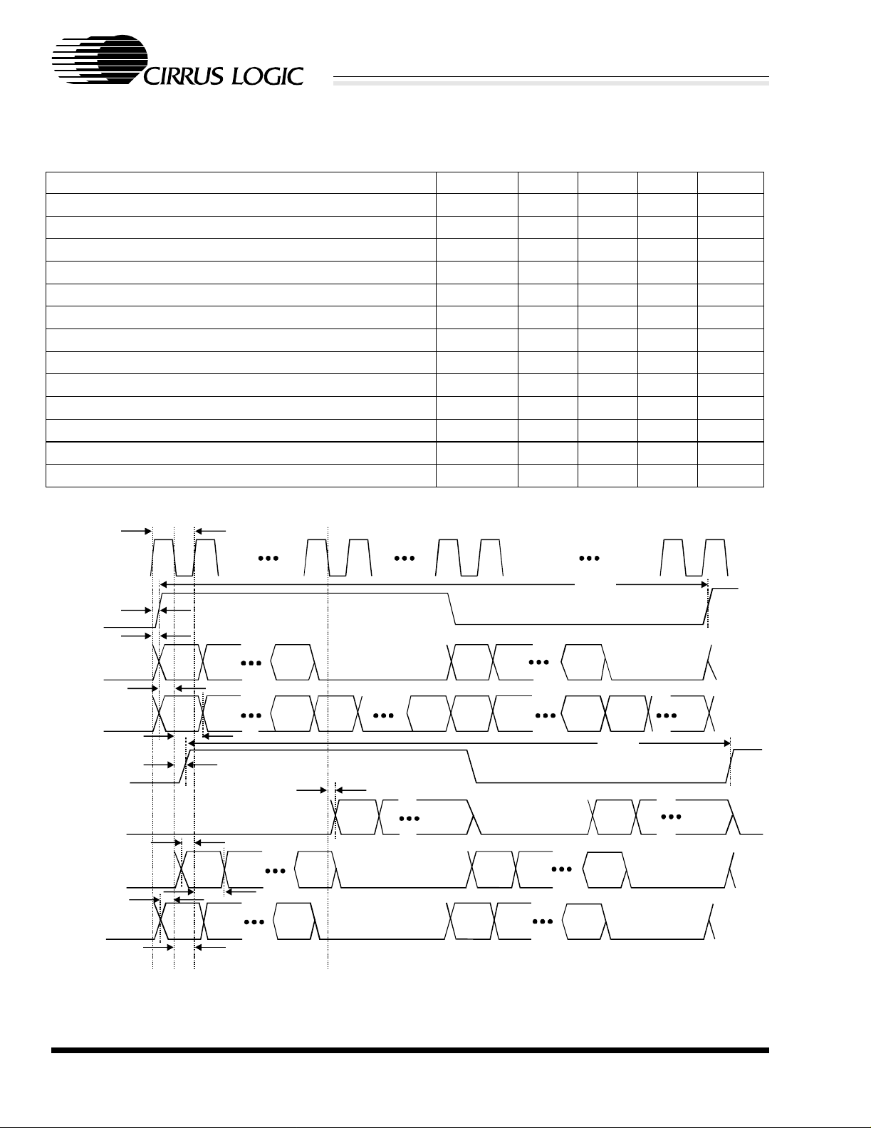
CS4610/11 + CS423X CONFIGURATION (T
= 0 to 70° C;
A
PCIVDD = CVDD = CRYVDD = 3.3 V; VDD5REF = 5 V; PCIGND = CGND = CRYGND = 0 V;
Logic 0 = 0 V, Logic 1 = 3.3 V; Timing reference levels = 1.4 V; unless otherwise noted)
Parameter Symbol Min Typ Max Unit
SCLK input cycle time t
FSYNC input cycle time t
SCLK rising to FSYNC transition t
SCLK rising to SDOUT valid t
SDIN valid to SCLK falling t
SDIN hold after SCLK falling t
LRCLK output cycle time t
SCLK falling to LRCLK transition t
SCLK falli n g to S DO 2 /S D O3 valid t
SDIN2 valid to SCLK rising (SI2F1-0: 00) t
SDIN2 hold after SCLK rising (SI2F1- 0: 00) t
SDIN2 valid to SCLK falling (SI2F1-0: 01) t
SDIN2 hold after SCLK fallin g (SI2F1-0: 01) t
sclk
fsync
pd1
pd2
s1
h1
lrclk
pd3
pd4
s2
h2
s3
h3
320 354 - ns
20480 22676 - ns
-20 - 20 ns
-2545ns
30 - - ns
30 - - ns
20480 22676 - ns
-2545ns
-2545ns
30 - - ns
30 - - ns
30 - - ns
30 - - ns
SCLK
FSYNC
SDOUT
SDIN
LRCLK
SD02/SD03
SDIN2
SDIN2
t
s1
t
t
s3
h1
15
15
t
s2
19 18
t
sclk
t
pd1
t
pd2
14 0
14
t
pd3
17
16
t
fsync
15
14
0
15
t
pd4
15
0
t
h2
0
0
15
14
0
17 16
19
18
0
15
00
t
lrclk
15
0
0
0
t
h3
Figure 3. CS4610/11 and CS423x Link and 6 Channel Output Timing Diagram
6 DS241PP5
CS4610/11
CrystalClear™ SoundFusion™ PCI Audio Accelerator
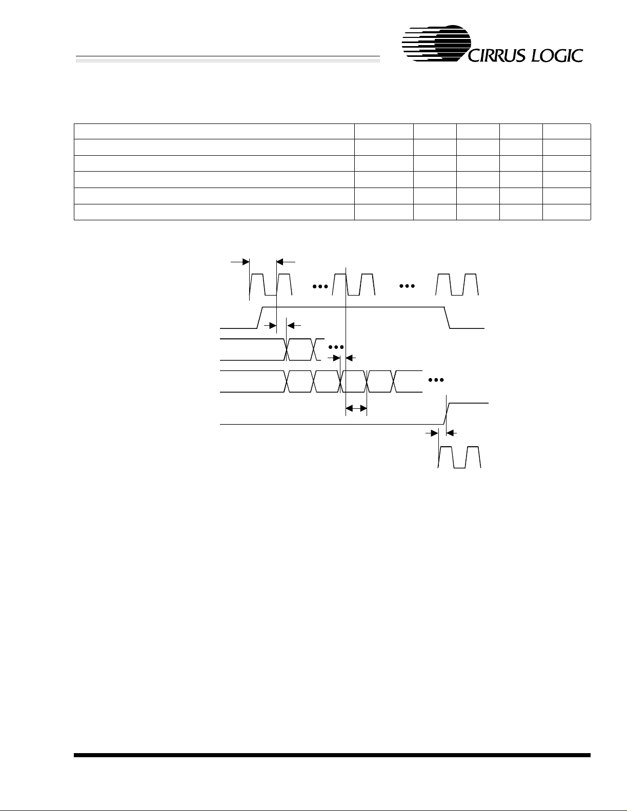
AC’97 SERIAL INTERFACE TIMING (T
VDD5REF = 5 V; VDD5REF = 5 V; PCIGND = CGND = CRYGND = 0 V; Logic 0 = 0 V, Logic 1 = 3.3 V;
Timing reference levels = 1.4 V; unless otherwi se noted)
Parameter Symbol Min Typ Max Unit
ABITCLK cycle time t
ABITCLK rising to ASDOUT valid t
ASDIN valid to ABITCLK falling t
ASDIN hold after ABITCLK falling t
PCICLK rising to ARST# valid t
t
= 0 to 70° C; PCIVDD = CVDD = CRYVDD = 3.3 V;
A
aclk
pd5
s5
h5
pd6
aclk
78 81.4 - ns
-1725ns
15 - - ns
5--ns
-10- ns
ABITCLK
ASYNC
ASDOUT
t
pd5
t
s5
ASDIN
ARST#
PCICLK
t
h5
Figure 4. AC’97 Configuration Timing Diagram
t
pd6
DS241PP5 7
CS4610/11
CrystalClear™ SoundFusion™ PCI Audio Accelerator
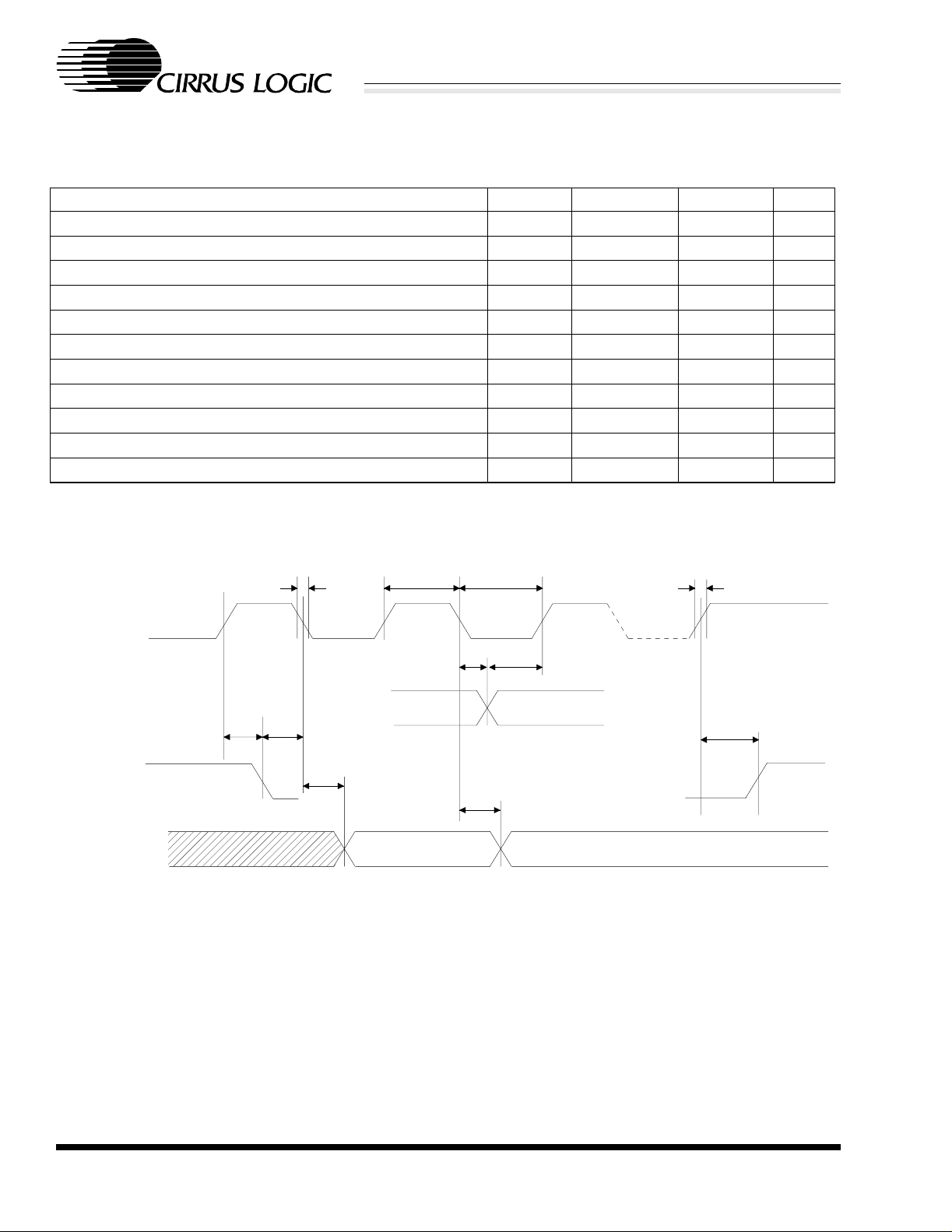
EEPROM TIMING CHARACTERISTICS Note 4. (T
= 0 to 70 °C, PCIVDD = CVDD = CRYVDD =
A
3.3 V; VDD5REF = 5 V; VDD5REF = 5 V; PCIGND = CGND = CRYGND = 0 V; Logic 0 = 0 V, Logic 1 = 3.3 V;
Timing reference levels = 1.4 V; PCI clock frequency = 33 MHz; unless otherwise noted)
Parameter Symbol Min Max Units
EECLK Low to EEDAT Data Out Valid t
St art Condition Hold Ti me t
EECLK Low t
EECLK High t
St art Condition Setup Ti me (for a Repeated St art Condition) t
EEDA T In Hold Time t
EEDAT In Setup Time t
HD:STA
LEECLK
HEECLK
SU:STA
HD:DAT
SU:DAT
EEDAT/EECLK Rise Time (Note 16) t
EEDAT/EECLK Fall Time t
Stop Condition Setup Time t
SU:STO
EEDAT Out Hold Time t
AA
R
F
DH
07.0
5.0 10 10 -
5.0 -
0-
250 - ns
-1
-300ns
5.0 -
0-
µ
s
µ
s
µ
s
µ
s
µ
s
µ
s
µ
s
µ
s
µ
s
Notes: 16. Rise time on EEDAT is determined by the capacitance on the EEDAT line wi th all connected gat es and
the required external pull-up resistor.
t
t
F
HEECLK
t
LEECLK
t
R
EECLK
EEDAT (IN)
EEDAT (OUT)
EEDAT (OUT)
t
SU:STA
t
HD:DAT
t
HD:STA
t
AA
Figure 5. EEPROM Timing
t
SU:DAT
t
SU:STO
t
DH
8 DS241PP5

CS4610/11
CrystalClear™ SoundFusion™ PCI Audio Accelerator
OVERVIEW
The CS4610 and CS4611 are high performance audio accelerator DSPs for the PCI bus. These devices, combin ed with applic ation and drive r software,
provide a com plete syste m solutio n for cost e ffec-
®
tive acceleration of Windows
DirectSound3D, DirectInput, DirectShow, MIDI
playback vi a Wav etable Sy nthesis with reverbe ration and chorus effect s processing, and more.
The CS4610 is a high-performance, full-featured
version of the So undF usion au dio acce le rato r. The
CS4611 is a r educed-cost ver sion of the CS46 10.
The CS4611 has a lower max clock speed and does
not support AC-3 o r MPEG-2. Please refer to the
OEM Software Reference Manual for more details.
There are t hree main func tional blocks wi thin the
CS4610/11: the Stream Processor, the PCI Interface, and the DMA Engine. The Stream Processor
(SP) is a high speed custom Digital Signal Processor (DSP) core designed by Cirrus Logic, Inc. specifically for audio signal processing. This
extremely powerful DSP core is capable of running
complex algorithms such as Dolby Digital AC-3 or
MPEG-2 audio decod ing for applications such as
DVD movie playback or gaming. The SP is capable
of running a numbe r o f diffe rent sign al pro cessin g
algorithms simultaneously. This high concurrency
capabilit y is valuable for applications such as im mersive 3D games, which may play a n umb er of DirectSound stre ams, a number o f DirectSoun d3D streams,
and a MIDI music sequence simultan eo usly.
DirectSound,
to meet th e requireme nts of a variety of d ifferent
applications, such as DirectX™ games, DVD movie playback, or DOS applications. This RAM-based
architec ture also prov ides a mean s for future system upgrades, allowin g the addi tion o f new or upgraded functio nal ity through software up da te s.
The CS4610/11 provides an extremely efficient bus
mastering interfa ce to the PC I bus. The P CI Inte rface functi on allows eco nom i ca l burst mode t r ansfers of audio data between host system memory
buffers and t he CS4610/11 device. Program code
and parameter data are also transferred to the
CS4610/11 over the PCI Interface.
The CS4610/11 DMA Engine provides dedicated
hardware to manage transfer of up to 96 concurrent
audio/data stream s to a nd from h ost me mory buf fers. The DMA Engine provi des hardware scattergather support, allowing simple buffer allocation
and management. This implementation improves
system efficiency by minimizing the number of
host interrupts.
The CS4610/11 supports a variety of audio I/O
configurations, including direct connection to the
CrystalClear CS 423x Codecs or to an AC’97 Co dec such as the CrystalClear CS4297. The system’s
flexibility is further enhan ced by the inclusion of
auxiliary ADC and DAC ports, a bi-direction al serial MIDI port, a jo ysti ck po rt, a hardwa re vo lum e
control inte rface, and a serial data port which allows con nec t ion of an o pti onal e xter nal EEP R OM
device.
Separate RAM memori es are include d on-chip for
the SP program code (Program RAM), paramete r
data (Parameter RAM), and audio sample data
(Sample RAM). A small ROM memory (Coefficient ROM ) is included t o store fixed coef ficient
data required for the sample rate conversion and
audio decompression algorithm s.
The RAM-based DSP architecture of the
CS4610/11 ensures maximum system flexibility.
The software function/fe ature mix ca n be adapte d
DS241PP5 9
The block di agram in Figure 6 depi cts a motherboard audio subsystem based on the CS4610/11
and the CS423x. This approach features the proven
ISA legacy suppo rt of the CS423x Co decs (which
include the CS423xB family as well as the CS4235
and CS4239 d evices). The CS423x provides DOS
applications with hardware compatibility for the
Sound Blaster Pro™, OPL3, and MPU-401 register
sets. In this configuration, the CS423x also provides the system joystick interface. The CS423x

CS4610/11
CrystalClear™ SoundFusion™ PCI Audio Accelerator
provides all Analog-to-Digital conversion (ADC)
and Digital-to-Analog conversion (DAC) functions. Digital audio is transferred between the
CS423x and t he CS4610/11 over a p roprietary bidirectional serial data link between the two devices.
MIDI data from the CS423x MPU-401 UART is
also transferred serially to the CS4610. DOS applications can directly address the CS423x audio
functions on the ISA bus. Win dows DirectX au dio
applications will address the PCI-based CS4610/11
device throug h W in dows Di rec tX drivers, wherein
the CS423x is utilized as the external Codec for analog I/O.
CPU
Host Bridge /
Mem Control
PCI Bus
A system diagram depicting connection of the
CS4610/11 to the CrystalClear CS4297 AC’97 Codec is given i n Figure 7. All analog au dio inputs
and outputs are connected to the AC’97 Codec. Audio data is passed between the AC’97 Codec and
the CS4610/11 over the serial AC-Link. The
CS4610/11 pr ovides a hardware i nterfac e for con nection of a joystick and MIDI devices. Legacy audio support under a Windows DOS Box is provided
via virtualization of the Sound Blaster
™, OPL3
FM synthesizer and MPU-401 MIDI interface registers.
Host Memory
Optional
Opt. CS4333 DACs
Surround
Outputs
CS423x
Motherboard
Audio
Audio Out
Audio In
ISA
Bridge
CS4610/11
Accelerator
Digital
Link
ISA Bus
Figure 6. CS4610/11 + CS423x Motherboard Audio Configuration
CPU
CS4610/11
Accelerator
Host Bridge /
Mem Control
Host Memory
PCI Bus
AC ’97
Codec
Audio Out
Audio In
Figure 7. CS4610/11 + AC ‘97 Codec Configuration
10 DS241PP5

CS4610/11
CrystalClear™ SoundFusion™ PCI Audio Accelerator
Stream Processor DSP Core
The CS4610/11 Stream Processor (SP) is a custom
DSP core design optimized for processing and synthesizing digital audio data streams. The SP features a So mewhat Lo ng Instruct ion Multip le Data
(SLIMD) modified dual Harvard archite cture. The
device uses a 40-bit instruct ion word a nd ope rates
on 32-bit data words. The SP core is conservatively
rated at 300 Million Instruc tions per second (300
MIPS) when running a t a 100 MHz inte rnal cloc k
speed (CS4611 run s at 85 MHz) . The SP in cludes
two Multip ly-Accumulate (MA C) blocks and one
16-bit Arithmetic and Logic Unit (ALU). The
MAC units perform 20-bit by 16-bit multiplies and
have 40-bit accumulators, providing higher quality
than typical 16-bit DSP architectures.
PLL and Clock Control
The CS4610/11 includes a programmable Phase
Locked Loop (PLL) circuit which generates the
high frequency internal SP c lock from a lower frequency input clock. The PLL input may come from
the CS4610/11 crystal oscillator circuit or the serial
port clock (ASCLK/SCLK). The CS4610/11 Clock
Control circuitry allows gating of clocks to various
internal functional blocks to conserve power during
power conserva tion modes, as well as during nor mal modes of operation when no tasks ar e being
executed.
Host Interface
The CS4610/ 11 host inte rface is comp rised o f tw o
separate interface blocks which are memory
mapped into host address space. The CS4610/11
interface blocks can be located anywhere in the
host 32-bit physical address space. The interface
block locations are defined by t he addresses programmed into the tw o Base Address Registers in
the CS4610/11 PCI Configuration Space. These
base addresses are n orm a ll y set up by the system’s
Plug and Play B IOS. The fir st interface block (lo -
cated using Base Address 0) is a 4 kByte re gister
block containing general purpose configuration,
control, and status registers for the device. The second interface block (located using Base Address 1)
is a 1 MByte block which maps all of the
CS4610/11 int ernal RAM memo ries (SP Program
RAM, Parameter RAM, and Sampl e RAM), along
with the SP debug registers, into host memory
space. This allows the host to directly peek and
poke RAM locat ions on the device. T he relationship between the Base Address Registers in the
CS4610/11 PCI Configuration Space and the host
memory map is de pi cted in Figure 8.
CS4610/11 PCI Interface
The CS4610/1 1 provides a bus maste ring PCI bus
interface which comp lies with the PCI Local B us
Specification version 2.1.
PCI Bus Transactions
As a target of a PCI bus transaction, the
CS4610/11 supports the Memory Read (from
internal registers or memory), Memory Write (to
internal r egisters or m emory), Configur ation Re ad
(from CS4610/11 configuration registers),
Configuration Write (to CS4610/11 configuration
registers), Memory Read Multiple (aliased to
Memory Read), Memory Read Line (aliased to
Memory Read), and the Memory Write and
Invalidate (aliased to Memory Write) transfer
cycles. The I/O Read, I/O Write, Interrupt
Acknowledge, Special Cycles, and Dual Address
Cycle transactions are not support ed.
As Bus Master, the CS4610/11 generates the Memory Read Multiple and Memory Write transactions.
The Memory Read , Configuration Read, Configu ration Write, Mem ory Read Line, Memory Write
and Invalidat e, I/O Read, I/O Write, Interrupt Ac knowledg e, S pecial Cycles, and Dual Address Cycle transacti o ns are not generated.
DS241PP5 11

Device PCI Config Space
Device ID / Vendor ID
00h
04h
08h
0Ch
10h
14h
Status / Command
Class Code / Revision
Misc Control
Base Address Register 0
Base Address Register 1
CS4610/11
CrystalClear™ SoundFusion™ PCI Audio Accelerator
Direct I/O Register s
(Memory Mapped, 4KB)
Direct Me mory Interfac e
(Memory Mapped, 1KB)
Figure 8. CS4610/11 Host Interface Base Address Registers
Initiator Target Type PCI Dir
Host Registers (BA0) Mem W ri te
Host Registers (BA0) Mem Read
Host Memories (BA1) Mem Write
Host Memories (BA1) Mem Read
Host Config Space 1 Config Write
Host Config Space 1 Config Read
DMA Host System Mem Write
DMA Host System Mem Read
Table 1. CS4610/11 PCI Interface Transaction Summary
The PCI bus transactions supported by the
CS4610/11 device are summarized in Table 1. Note
that no Target Abort conditions are signalled by the
device. Byte, Word, and Doublewo rd transfers are
supported for Con figuration Space ac cesses. Only
Doubleword transfers are supported for Register or
In
Out
In
Out
In
Out
Out
In
Memory area accesses. Burst ing is not supported
for host-i nitiated tran sfers to/fr om the CS4 610/11
internal register space, RAM memory space, or
PCI configuration space (disconnect after first
phase of transaction is completed).
12 DS241PP5

CS4610/11
CrystalClear™ SoundFusion™ PCI Audio Accelerator
Configuration Space
The content and format of the primary PCI Configuration Space for the CS4610/11 device is given in
Table 2.
Byte 3Byte 2Byte 1Byte 0Offset
Device ID: R/O, 6001h Vendor ID: R/O, 1013h 00h
St atus Register, bits 15-0:
Bit 15 Detected Parity Error: Error Bit
Bit 14 Signalled SERR: Error Bit
Bit 13 Received Master Abort: Error Bit
Bit 12 Received Target Abort: Error Bit
Bit 11 Signalled Target Abort: Error Bit
Bit 10-9 DEVSEL Timing: R/O, 01b (medium)
Bit 8 Data Parity Error Detected: Error Bit
Bit 7 Fast Back to Back Capable: R/O 0
Bit 6-0UDF, 66MHz, Reserved: R/O 0000000
Reset Status State: 0200h
Write of 1 to any error bit position clears it.
Class Code: R/O 040100h
Class 04h (multimedia device), Sub-class 01h (audio), Interface 00h
BIST: R/O 0 Header Type:
Bit 7: R/O 0
Bit 6-0: R/O 0 (type 0)
Base Address Register 0
Device Control Register space, memory mapped. 4 kByte size
Bit 31-12: R/W, default 0. Compare address for register space accesses
Bit 11 - 4: R/O 0, specifies 4 kByte size
Bit 3: R/O 0, Not Prefetchable (Cacheable)
Bit 2-1: R/O 00, Location Type - Anywhere in 32 bit address space
Bit 0: R/O 0, Memory space indicator
Command Register, bits 15-0:
Bit 15-10: Reserved, R/O 0
Bit 9 Fast B2B Enable: R/O 0
Bit 8 SERR Enable: R/W, default 0
Bit 7 Wait Control: R/O 0
Bit 6 Parity Error Response: R/W, default 0
Bit 5 VGA Palette Snoop: R/O 0
Bit 4 MWI Enable: R/O 0
Bit 3 Special Cycles: R/O 0
Bit 2 Bus Master Enable: R/W, default 0
Bit 1 Memory Space Enable: R/W, default 0
Bit 0 IO Space Enable: R/O 0
Latency Timer:
Bit 7-3: R/W,default 0
Bit 2-0: R/O 0
04h
Revision ID: R/O 01h 08h
Cache Line Size:
R/O 0
0Ch
10h
Base Address Register 1
Device Memory Array mapped into host syst em memory space, 1 MByte size
Bit 31-20: R/W, default 0. Compare address for memory array accesses
Bit 19 - 4: R/O 0, specifies 1 MByte size
Bit 3: R/O 0, Not Prefetchable (Cacheable)
Bit 2-1: R/O 00, Location Type - Anywhere in 32 bit address space
Bit 0: R/O 0, Memory space indicator
Base Address Register 2: R/O 00000000h, Unused 18h
Base Address Register 3: R/O 00000000h, Unused 1Ch
Base Address Register 4: R/O 00000000h, Unused 20h
Base Address Register 5: R/O 00000000h, Unused 24h
Table 2. CS4610/11 PCI Configuration Space 1
DS241PP5 13
14h

CS4610/11
CrystalClear™ SoundFusion™ PCI Audio Accelerator
Byte 3Byte 2Byte 1Byte 0Offset
Cardbus CIS Pointer: R/O 00000000h, Unused 28h
Subsystem ID
R/O 0000h
see
Subsystem Vendor ID Fields
Expansion ROM Base Address: R/O 00000000h, Unused
Reserved: R/O 00000000h
Reserved: R/O 00000000h
Max_Lat: R/O 18h
24 x 0.25uS = 6 uS
Min_Gnt: R/O 04h
4 x 0.25uS = 1uS
section
Table 2. CS4610/11 PCI Configuration Space 1
Subsystem Vendor ID
R/O 0000h
see
Interrupt Pin:
R/O 01h, INTA used
Subsystem Vendor ID Fields
The Subsystem ID and Subsystem Vendor ID
fields in the C S4610/11 PCI Con figuration Space
default to value 0000h unless an external EEPROM
device is d etec ted or un le ss the host ha s writ ten to
the appropriate internal register to program the values. When pro grammed thr ough the EE PROM all
four bytes can be written. However, when programming though th e host interface (BIOS code),
only the Subsyste m Vendor ID (bytes 1 and 0) can
be programmed. The Subsystem ID (bytes 3 and 2)
is forced to the most significant byte (byte 1) of the
Subsystem Vendor ID. Therefore, when loaded
though host cod e, byt es o ne, tw o an d th ree wil l all
have the same value.
CS4610/11 Interrupt Signal
The CS4610/11 PCI Interface includes an interrupt
controller function which receives interrupt requests from multiple sources within the CS4610/11
device, and presents a single interrupt line (INTA#)
to the host system. Interrupt control registers in the
CS4610/11 pro vide the host i nterrupt servic e routine with the ability to identify the source of the interrupt and to clear the interrupt sources. In the
CS4610/11, the single external interrupt is expand-
2Ch
Subsystem Vendor ID Fields
Interrupt Line :
R/W, default 0
(Continued)
section
30h
34h
38h
3Ch
ed by the use of “virtual channels”. Each data
stream whic h is read from or written to a modul o
buffer is assigned a virtual channel number. This
virtual channel number is signalled by the DMA
subsystem anytime the associated modulo buffer
pointer passes the mid-point or wraps around. Virtual channels are also used for message passing between the CS4610/ 11 and the host.
Serial Port Configurations
The CS4610/11 provides a flexible Serial Audio
Interface which allows connection to external Analog-to-Digital C onverters (ADCs), Digi ta l-to-Analog Converters (DACs) or Codecs (combined ADC
and DAC functions) in several different configurations. The CS4610/11 serial audio interface includes a primary in put/output port with ded icated
serial data pins (SDIN, SDOUT), two auxiliary audio output ports (SDO2, SDO3) which sha re pins
with the joystic k interface button inp ut functions,
and one aux iliary audio inp ut port (SDIN2). Eac h
of these digital au dio input and output pins carr y
two channels of audio data. These two channels
may compri se the left and right chan nels of a st ereo
audio signal, or they may be two independent monaural audio signa ls.
14 DS241PP5

CS4610/11
CrystalClear™ SoundFusion™ PCI Audio Accelerator
Each digital audio channel is internally buffered
through a 16 sample x 20-bit FIFO. The data format
for the serial di gital audio ports varies d epending
on the configuration. The primary configurations
supported include a CS4610/1 1 plus CS423x con figuration for motherboard audio, a CS4610/11
plus CS423x configuration with full 5.1 channel
output cap abil ity, and an AC ’97 c ontrol ler c on fig uration (CS4610/11 plus an AC’97 Codec).
CS4610/11 + CS423x Motherboard Audio Accelerator
A system block diagram for the CS4610/11 plus
CS423x configuration is given in Figure 6. This
configuration utilizes a proprietary bi-directional
digital aud io link between the CS4610/11 and the
CS423x. The conn ection be tween these d evices is
depicted in Figure 9.
In the CS4610/11 plus CS423x configura tion, the
CS423x is the se rial port t iming m aster. T he seri al
port runs at a fixed 44.1 kHz sampl ing rate, and the
2.822 MHz SCLK output from the CS423x is selected
as the CS4610/11 PLL clock generator input.
Note that in this configuration the SDIN signal carries two stereo streams from the CS423x to the
CS4610/11: the CS423x ADC data and the CS423x
output data. The SDOUT signal carries the
CS4610/11 final output to the CS423x DACs.
SDIN and SDOUT transitions occur on rising edges of SCLK (SDIN is sampled on falling edges of
SCLK). The data is transmitted in left-justified format, MSB first, 16-bit data, with 3 2 clock cycles
for each phase of the FSYNC signal. FSYNC transitions occur on rising edges of SCLK, the FSYNC
high phase indicates left channel data on SDIN and
SDOUT while the FSYNC low phase indicates
right channel data. The SDOUT signal carries 16
bits of data followed by 16 bits of zero pad for each
channel (left and right). The SDIN signal carries 16
bits of ADC data followe d by 16 bits of playback
data for each channel (left and right). The serial
port clock and data timing relationship for this configuration i s ind ic ated i n Figure 10. The cl ock and
data signal functions for this configuration are
summarized in Table 3.
Motherboard Configuration with 5.1 channel output capability (CS4610 only)
This configurat ion is the sam e as the CS 4610 plus
CS423x motherboard accelerator configuration
with the add ition of t wo Crystal ™ CS43 33 Stere o
PLL/
Clock G en
ABITCLK/SCLK
ASYNC/F SY NC
ASDOUT/SDO U T
ASDIN/SDIN
MIDIIN
CS4610/11 PCI
Accelerator
Figure 9. CS4610/11 + CS423x Connection Diagram
DS241PP5 15
64Fs (2.822 MH z)
44.1 kHz ( fix ed)
16.9344 MHz
SCLK
FSYNC
SDIN
SDOUT
MIDOUT
CS423x
ISA C odec

FSYNC
CS4610/11
CrystalClear™ SoundFusion™ PCI Audio Accelerator
SCLK
SDOUT
SDIN
Pin Name Direction Functional Description
SCLK Input Main timing driver for digital audio l ink, both edge s used i nternal ly fo r t iming. Also f uncti ons
FSYNC Input Framing signal for digital audio link, high time indicates left channel data and low time indi-
SDOUT Output Primary output port serial d ata pin. This data is the CS4610/11 output stream going to the
SDIN Input
15 14 13
DAC 16 Clocks
14 13
15
ADC 16 Clocks DAC 16 Clocks ADC 16 Clocks DAC 16Clocks
Figure 10. Serial Audio Port Format for CS4610/11 + CS423x Configuration
as the source to the PLL for inter nal clock generation.
cates right channel dat a. Frame is sampled on the falling edge of the SCLK input.
CS423x device. The serial data on this pin transi tion s on the rising edge of the SCLK input.
Primary input port seri al data pin. T his data contain s bot h C S423x ADC data and the CS423x
output data. The serial data on this pin i s sam pled on the falling edge of the SC LK input.
Table 3. Serial Audio Port Signal Summary for CS4610/11 + CS423x Configuration
...
... ... ... ...
0
0
...
15 14
13 0
...
15 14
15 14 13
13 0
DAC 16 Clocks
0
Right DataLeft Data
...
15 14 13
15
0
15
DACs to expand the audio output capability to six
channels. This expanded output capability is useful
for applicat ions where discrete 5.1 channel o utput
is desired for Dolby AC-3 audio programs. The
connection diagram for the additional CS4333
DACs is given in Figure 11. The CS4333 DACs
share the SCLK output from the CS423x w ith the
CS4610. The CS4333 DACs also receive a 16.9344
MHz MCLK signal from the CS423x. Note that the
CS423x MCLK o utput has limited drive stren gth
and should be buffered in this application. The LRCLK framing clock and the SDO2/SDO3 digital
audio outp uts are pro vided fr om the CS 4610. The
SDO2 and SDO3 transitions occur on falling edges
of SCLK (the primary output SDOUT transitions
on rising edges of SCLK). LRCLK tra nsitions occur on falling edges of SCLK, with the LRCLK
high phase ind icating left channel dat a present on
SDO2/SDO3. SDO2/SDO3 data is right justified,
with 16 bits of zero pad followed by 16-bits of data,
transmitted MSB first. There are 64 SCLKs per
LRCLK, and MCLK r uns at 384× the frame rate.
The serial port clock and data timing relationship
for this configuration is indicated Figure 12. The
clock and da ta signal functions for this config uration are summarized in Table 4.
AC’97 Controller Configuration
In this configuration the CS4610/11 functions as an
AC’97 controller. The CS4610/11 communicates
with an AC’97 Codec, such as the CrystalClear
CS4297, over the AC-link as specified in the Intel
Audio Codec ‘97 Specification version 1.03. A
block diagram for the AC’97 Controller Configuration is given in Figure 7. The signal connections between the CS4610/11 and the AC’97 Codec are
indicated in Figure 13. In this configuration, the
AC’97 Codec is the timing m aster for the digital
audio link. The CS4610/11 ASDOUT output supports data transmission on all 10 pos sible sample
®
16 DS241PP5

CS4610/11
CrystalClear™ SoundFusion™ PCI Audio Accelerator
PLL/
Clock Gen
JBB1/LRCLK
JAB1/SDO2
JAB2/SDO3
ABITCLK/SCLK
ASYNC/FSYNC
ASDOUT/SDOUT
ASDIN/SDIN
MIDIIN
Analog Out Pair 2
Surround Left
Surround Right
Analog Out Pair 3
Center
Sub
A
AOU TR
O
U
TL
433xDAC
L
SDA
MCLK
R
SC LK
CLK
TA
AOU TR
AOU
T
433xDAC
L
SDATA
LRC LK
SC LK
MCL
K
Analog Out Pair 1
L
OUT
16.9344
MCLK
Left
Right
ROU T
SCLK
FSYNC
SDIN
SDOUT
MIDOUT
CS4610PCI
Accelerator
16.9344 MHz
CS423x
ISA Codec
Figure 11. CS4610 + CS423x Expanded 6-Channel Output Configuration
Pin Name Direction Functional Description
SCLK Input Main timing driver for digital audio link, both edges used internally for tim-
ing. Also functions as the source to the PLL for internal cl ock generation.
FSYNC Input Framing signal for digital audio link, high time indicates left channel data
and low time indicates right channel data. FSYNC is sampled on the falling
edge of the SCLK input.
SDOUT Output Primary output port serial data pin. This data is the CS4610 output stream
going to the CS423x DACs. SDOUT transitions on the rising edge of the
SCLK input.
SDIN Input Primary input port serial data pin. Thi s data contains both CS423x ADC
data and the CS423x output data. SDIN is sampled on the falling edge of
the SCLK input.
LRCLK Output Framing signal for external 4333 DACs, high time indicates left channel
data and low time indicates right channel data. LRCLK transitions on the
falling edge of the SCLK input.
SDO2, SDO3 Output Second and third output port seria l dat a pins. These output streams are
the expanded output cha nnels beyond the CS423x left / right pai r. The
serial data on these pins tr ansition on the falling edge of the SCLK input.
Note that this is a DIFFERENT SCLK edge than the one for the SDOUT
pin.
Table 4. Serial Audio Port Signal Summary for CS4610 + CS423x Expanded Output Configuration
DS241PP5 17

FS Y NC
CS4610/11
CrystalClear™ SoundFusion™ PCI Audio Accelerator
Left Data Right Data
SC L K
SD O UT
SD IN
LRCL K
SD O 2
SD O 3
Figure 12. Serial Audio Port Format for CS4610 + CS423x Expanded Output Configuration.
14
15
DAC 16 Clocks
ADC 16 Clocks DAC 16 Clocks ADC 16 Clocks DAC 16 Clocks
0 15 14 13 0 15 14 13 0
13
131415
...
... ...
0
0
DAC 16 Clocks
slots (output slots 3 - 12). The CS 4610/11 ASD IN
input supports re ce iving of audio sa mple data on 6
input sample slots (input slots 3 - 8). The SDO2,
SDO3 serial outputs and the SDIN2 serial input are
not supported in this config ura tion.
15 14 13
DAC 16 Clocks
0131415
...
0
... .........
131415
DAC 16 Clocks
15
01314150
15
operating in the traditional “polled” mode, but also
provides a “ha rdware ac cele rated” mode of ope ration wherein inte rnal counters assist the host with
coordinate position determination. The joystick
schematic is illustrated in Figure 14.
MIDI Port
In the AC’97 controller configuration, the
CS4610/11 provides a bi-directional MIDI interface to allow conn ection of ex ternal MIDI devices.
The CS4610/11 MIDI interface includes 16-byte
FIFOs for the MIDI transmit and receive paths.
EEPROM Configuration Interface
The CS4610 /11 EEPROM configura tion interfa ce
allows the co nnection of a n optional external E EPROM device to pr ovide power-up configuratio n
information. The external EEPROM is not required
for proper operation of the CS4610 . However, in
some applications p ower-up config urati on sett ings
Joystick Port
In the AC’97 controller configuration, the
CS4610/11 provides a joystick port. The
CS4610/11 joystick port provides four “coordinate” chan ne ls and four “button” channels of input
capability. The coordinate channels provide joystick positional information to the host, and the button channels provide user button event
information. The joystick interface is capable of
18 DS241PP5
other than the CS4610/11 device default values
may be require d to support specific operati ng system compatibility requirements (the CS4610/11
default is the CS4610/11 + CS423x configuration).
These defaul t values can b e programmed through
BIOS code or by using the external EEPROM.
After a hardware r es et, an in ter nal state machine in
the CS4610/11 will automatically detect the pres-

CS4610/11
CrystalClear™ SoundFusion™ PCI Audio Accelerator
PLL/
Clock Gen
ABITCLK/SCLK
ASYNC/ FSYNC
ASDOUT/SDOUT
ASDIN/SDIN
ARST#
MIDIIN
MIDIOUT
JACX, JACY, JBCX, JBCY
JAB1, JAB2, JBB1, JBB2
CS4610/ 11
Figure 13. CS4610/11 - AC ‘97 Codec Connection Diagram
DSP
JAB1
JBB1
JACX
JBCX
5.6 nF
JBCY
JACY
JBB2
JAB2
4.7 k
MIDIOUT
12.288 MHz
48 kHz
24.576 MHz
BIT_CLK
SYNC
SDATA_OUT
SDATA_IN
RESET#
AC’ 97 Cod ec
CS4297
Joystick/MIDI Port
+5 V
1
4.7 k
Ω
Ω
2.2 k
Ω
2.2 k
5.6 nF
1 nF
2.2 k
Ω
5.6 nF
Ω
4.7 k
2.2 k
5.6 nF
4.7 k
1 nF
Ω
Ω
Ω
1 nF
4.7 k
Ω
1 nF
9
2
10
3
11
4
12
5
13
6
14
7
15
8
MIDIIN
Figure 14. Joystick Logic
DS241PP5 19

CrystalClear™ SoundFusion™ PCI Audio Accelerator
CS4610/11
4.7 k
Ω
EECLK
EEDAT
Figure 15. External EEPROM Connection
Serial
EEPROM
SCL
SDA
ence of an external EEPROM device and load the
Subsystem ID and Subsystem Vendor ID fields,
along with two by tes of general configur ation information, into int ern al re gi ste rs. A t p ower-up, the
CS4610/11 wi ll attempt to rea d from the extern al
device, and will check the data received from the
device for a valid signature head er. If the header
data is invalid, the data transfer is aborted. After
power-up, the host can read or write from/to the
EEPROM device by accessing specific registers in
the CS4610/ 11. Cirrus L ogic provid es software to
program the EEPROM.
The two wire interface for the optional external EEPROM devi ce is dep icted in Figure 15. Duri ng da ta
transfers, the data li ne (EEDAT ) can chan ge state
only while the clock signal (EECLK) is low. A
CS4610/11
state chan ge o f the data line whil e t he cl ock s ignal
is high indicates a start or stop condition to the EEPROM device.
The EEPROM device read access sequence is
shown in the Figure 16. The ti ming follows that of
a random read se quenc e. The CS4610/ 11 first per-
forms a “dummy” write operation, generating a
start condition followed by the slave device address
and the byte address of zero. The slave address is
made up of a device identifier (0xA) and a bank select (bits A2-A0). The CS4610/11 always begins
access at byte address zero and continues access a
byte at a ti me. The by te address automat ically increments by one unt il a st op cond ition is detec ted.
The CS4610/11 will read a total of seven bytes
from the EEPROM.
General Purpose I/O Pins
Many of the CS4610/11 signa l pins are int ernally
multiplexe d t o serve different functions depending
on the environment in which the device is being
used. Several of the CS4610/11 signal pins may be
used as general purpose I/O pins when not required
for other specific functions in a given ap plication.
Part
DSP
EEPROM
20 DS241PP5
Start
Address
S10100000A00000000AS1010000 1A Data Data P1A
Write
Figure 16. External EEPROM Read Access Sequence
Bank
Address
Start
Acknowledge Data
Part
Address
Read
Acknowledge
No
Acknowledge
Stop

CS4610/11
CrystalClear™ SoundFusion™ PCI Audio Accelerator
PIN DESCRIPTIONS
TEST 51
JACX 52
JACY 53
JBCX 54
JBCY 55
JAB1/SDO2 56
JAB2/SDO3 57
JBB1/LRCLK 58
JBB2/MCLK 59
MIDIIN 60
CVDD[2] 61
CGND[2] 62
MIDIOUT 63
CVDD[3] 64
CGND[3] 65
SDIN2/GPIO 66
CGND[4] 67
CVDD[4] 68
CRYVDD 69
VOLUP/XTALI 70
VOLDN/XTALO 71
CRYGND 72
VDD5REF 73
ABITCLK/SCLK 74
ASDOUT/SDOUT 75
ASDIN/SDIN 76
ASYNC/FSYNC 77
ARST# 78
EECLK/GPOUT 79
EEDAT/GPIO2 80
50 PCIVDD[7]
49 PCIGND[7]
48 AD[0]
47 AD[1]
46 AD[2]
45 AD[3]
44 AD[4]
43 AD[5]
42 AD[6]
41 AD[7]
40 PCIGND[6]
39 PCIVDD[6]
38 C/BE[0]#
CS461x-CM
37 AD[8]
36 AD[9]
35 AD[10]
34 AD[11]
33 AD[12]
32 AD[13]
31 PCIVDD[5]
30 PCIGND[5]
29 AD[14]
28 AD[15]
27 C/BE[1]#
26 PAR
25 SERR#
24 PERR#
23 STOP#
22 PCIGND[4]
21 PCIVDD[4]
20 DEVSEL#
19 CVDD[0]
18 CGND[0]
17 TRDY#
16 IRDY#
15 FRAME#
14 C/BE[2]#
13 CGND[1]
12 CVDD[1]
100-pin MQFP
11 AD[16]
10 AD[17]
9 AD[18]
8 PCIVDD[3]
7 PCIGND[3]
6 AD[19]
5 AD[20]
4 AD[21]
3 AD[22]
2 AD[23]
1 PCIGND[2]
RST# 82
GNT# 84
PCICLK 83
REQ# 85
PCIVDD[0] 86
PCIGND[0] 87
AD[31] 88
AD[30] 89
AD[29] 90
AD[28] 91
AD[27] 92
PCIGND[1] 93
PCIVDD[1] 94
AD[26] 95
AD[25] 96
AD[24] 97
IDSEL 99
C/BE[3]# 98
PCIVDD[2] 100
INTA# 81
DS241PP5 21

CS4610/11
CrystalClear™ SoundFusion™ PCI Audio Accelerator
TEST 65
JACX 66
JACY 67
JBCX 68
JBCY 69
JAB1/SDO2 70
JAB2/SDO3 71
JBB1/LRCLK 72
JBB2/MCLK 73
MIDIIN 74
CVDD[2] 75
CGND[2] 76
MIDIOUT 77
CVDD[3] 78
CGND[3] 79
80
81
82
83
84
85
86
87
SDIN2/GPIO 88
CGND[4] 89
CVDD[4] 90
CRYVDD 91
VOLUP/XTALI 92
VOLDN/XTALO 93
CRYGND 94
VDD5REF 95
ABITCLK/SCLK 96
ASDOUT/SDOUT 97
ASDIN/SDIN 98
ASYNC/FSYNC 99
ARST# 100
EECLK/GPOUT 101
EEDAT/GPIO2 102
64636261605958 PCIVDD[7]
103
104
105
106
107
108
57 PCIGND[7]
56 AD[0]
55 AD[1]
54 AD[2]
53 AD[3]
52 AD[4]
CS4610C-CQ
51 AD[5]
50 AD[6]
49 AD[7]
48 PCIGND[6]
47 PCIVDD[6]
46 C/BE[0]#
45 AD[8]
44 AD[9]
43 AD[10]
42 AD[11]
128-pin TQFP
41 AD[12]
40 AD[13]
38 PCIGND[5]
39 PCIVDD[5]
37 AD[14]
36 AD[15]
35 C/BE[1]#
34 PAR
33 SERR#
32 PERR#
31 STOP#
30 PCIGND[4]
29 PCIVDD[4]
28 DEVSEL#
27 CVDD[0]
26 CGND[0]
25 TRDY#
24 IRDY#
23
22
21
20
19
18
17
16
15 FRAME#
14 C/BE[2]#
13 CGND[1]
12 CVDD[1]
11 AD[16]
10 AD[17]
9 AD[18]
8 PCIVDD[3]
7 PCIGND[3]
6 AD[19]
5 AD[20]
4 AD[21]
3 AD[22]
2 AD[23]
1 PCIGND[2]
RST# 110
GNT# 112
INTA# 109
22 DS241PP5
REQ# 113
PCICLK 111
AD[31] 116
AD[30] 117
AD[29] 118
AD[28] 119
AD[27] 120
PCIVDD[0] 114
PCIGND[0] 115
PCIGND[1] 121
PCIVDD[1] 122
AD[26] 123
AD[25] 124
AD[24] 125
IDSEL 127
C/BE[3]# 126
PCIVDD[2] 128

CS4610/11
CrystalClear™ SoundFusion™ PCI Audio Accelerator
A ‘#’ sign suffix on a pin names indicates an active-low signal.
Note:
PCI Interface
AD[31:0] - Address/Data Bus, I/O
(M) pins 88-92, 95-97, 2-6, 9-11, 28-29, 32-37, 41-48
(Q) pins 116-120, 123-125, 2-6, 9-11, 36-37, 40-45, 49-56
These pins form t he multi plexed addr ess / data bus for th e PCI inte rface.
C/BE[3:0]# - Com mand Type / Byte En ables, I/O
(M) pins 98, 14, 27, 38; (Q) pins 126, 14, 35, 46
These four p ins are the multiplexed c ommand / byte enable s for the PCI interface. D uring the
address phase of a transaction, these pins indicate cycle type. During the data phases of a
transaction, active low byte enable information for the current data phase is indicated. These
pins are inputs du ring slave operation and they are outputs duri ng bus masteri ng operatio n.
PAR - Parity, I/O
(M) pin 26; (Q) pin 34
The Parity pin indicates even parity across AD[31 :0] and C_BE[3:0] for both a ddress and data
phases. The signal is delayed one PCI clock from either the address or data phase for which
parity is gener ated.
FRAME# - Cyc le Frame, I/O - Active Low
(M) pin 15; (Q) pin 15
FRAME# is driven by the current PCI bus master to indicate the beginning and duration of a
transaction.
IRDY# - Initiator Ready, I/O
(M) pin 16; (Q) pin 24
IRDY# is driven by the current PCI bus master to indicate that as the initiator it is ready to
transmit or rec eive data (c omplete the current da ta phase).
TRDY# - Ta rget Ready, I/O
(M) pin 17; (Q) pin 25
TRDY# is dri ven by the current PCI bus target to indicate that as the target dev ice it is ready to
transmit or rec eive data (c omplete the current da ta phase).
STOP# - Transition Stop, I/O
(M) pin 23; (Q) pin 31
STOP# is driven active by the current PCI bus target to indica te a request to the mast er to stop
the current tr ansaction.
IDSEL - Initialize Device Select, Input
(M) pin 99; (Q) pin 127
IDSEL is used as a c hip select during PCI configu ration read and wri te cycles.
DS241PP5 23

CrystalClear™ SoundFusion™ PCI Audio Accelerator
DEVSEL# - Device Select, I/O
(M) pin 20; (Q) pin 28
DEVSEL# is driv en by the PCI bus target device to indica te that it has decoded the addre ss of
the current tr ansaction a s its own chip se lect range.
REQ# - Master Request, Th ree-State Output
(M) pin 85; (Q) pin 113
REQ# indica tes to the system ar biter that this devic e is requesting access to the PCI bus. This
pin is high-imp edance whe n RST# is act ive.
GNT# - Master Grant, Input
(M) pin 84; (Q) pin 112
GNT# is driven by the system arbiter to indicate to the device that the PCI bus has been
granted.
PERR# - Pa rity Error, I/O
(M) pin 24; (Q) pin 32
PERR# is used for re porting data p arity errors on the PCI bus.
CS4610/11
SERR# - System Error, Open Drain Output
(M) pin 25; (Q) pin 33
SERR# is used for re porting addr ess parity errors an d other catast rophic system e rrors.
INTA# - Host Inte rrupt A (for SP), Open Drain Output
(M) pin 81; (Q) pin 109
INTA# is the level triggered interrupt pin dedicated to servicing internal device interrupt
sources.
PCICLK - PCI Bus Clock, Input
(M) pin 83; (Q) pin 111
PCICLK is the PCI bus clock for ti ming all PCI transact ions. All PCI synchronou s signals are
generated an d sample d relative to the risin g edge of t his clock.
RST# - PCI Device Reset
(M) pin 82; (Q) pin 110
RST# is the PCI bus m aster reset.
VDD5REF: Clean 5 V Power Supply
(M) pin 73; (Q) pin 95
VDD5REF is the power connec tion pin for the 5 V PCI pseudo supply for the PCI bus drivers.
24 DS241PP5

CS4610/11
CrystalClear™ SoundFusion™ PCI Audio Accelerator
PCIVDD[7:0] - PCI Bus Driver Power Supply
(M) pins 50, 39, 31, 21, 8, 100, 94, 86;
(Q) pins 58, 47, 39, 29, 8, 128, 122, 114
PCIVDD pins are the PCI driver p ower supply pin s.
PCIGND[7:0] - PCI Bus Driver Ground Pins
(M) pins 49, 40, 30, 22, 7, 1, 93, 87;
(Q) pins 57, 48, 38, 30, 7, 1, 121, 115
PCIGND pins are the PCI driver g round referen ce pins.
External Interface Pins
TEST - Test Mode Strap, Input
(M) pin 51; (Q) pin 65
This pin is sampled at reset for test mode entry. If it is high at reset, test mode is enabled. This
pin should norma lly be pull ed to ground i n a producti on design.
EEDAT/GPIO2 - External EEPROM Data / Genera l Purpose I/ O Pin 2, I/O Drai n
(M) pin 80; (Q) pin 102
Data line for externa l serial EEPROM co ntaining device co nfiguration data. When used with an
external EEPROM, a 4.7 kΩ pullup resistor is required. In designs without EEPROM
requirement s, this pin can b e used as a g eneral purp ose input or ope n drain outp ut.
EECLK/GPOUT - External EEPROM Clock / General Purpose Output Pin, Output
(M) pin 79; (Q) pin 101
Clock line for external serial EEPROM containing device configuration data. In designs
without EE PROM requi rements , this pin ca n be used as a general p urpose outp ut pin.
SDIN2/GPIO - Serial Data Input 2 / General Purpose I/O Pin, I/O
(M) pin 66; (Q) pin 88
This dual function pin defaults as a general purpose I/O pin. In non-AC’97 system
configurat ions, this pin can func tion as a seco nd stereo digital da ta input pi n if enabl ed.
VOLUP/XTALI - Volume Up Button / Crystal Input, Input
(M) pin 70; (Q) pin 92
This dual f unction pi n is eith er the vol ume up but ton control input o r the crysta l oscilla tor input
pin, depending on system configuration. When a crystal is used, it must designed for
fundamental mode, paral lel resonan t. This pin ma y also be use d as a genera l purpose inpu t if its
primary funct ion is no t needed.
VOLDN/XTAL O - Vol ume Down Button / Crystal Output, I/O
(M) pin 71; (Q) pin 93
This dual function pin is either the volume down button control input or the crystal oscillator
output pin, depend ing on system config uration. This pin may al so be used as a general purpose
input if its p rimary func tion is no t needed.
DS241PP5 25

CrystalClear™ SoundFusion™ PCI Audio Accelerator
Clock / Miscellaneous
CRYVDD - Crystal & PLL Power Supply
(M) pin 69; (Q) pin 91
Power pin fo r crystal o scillat or and in ternal p hase lock ed loop.
CRYGND - Crystal & PLL Ground Supply
(M) pin 72; (Q) pin 94
Ground pin for cryst al oscillator an d internal pha se locked loop.
JACX, JACY, JBCX, JB CY - Joystick A and B X/Y Coordinates, I/O
(M) pins 52, 53, 54, 55; (Q) pins 66, 67, 68, 69
These pins are the 4 axis coordinates for the joystick port. These pins may also be used as a
general purpose inputs or open drain out puts if their pri mary funct ion is not nee ded.
JAB1/SDO2 - Jo ystick A Button 1 / Se rial Data Output 2, I/ O
(M) pin 56; (Q) pin 70
This dual func tion pin defaults as JAB1 (button 1 input for joystick A). In non-AC’97 syste m
configuration s, this pin can function as a seco nd stereo digital data outpu t pin if enabled. This
pin can also be a general p urpose polled input if a se cond data ou tput stream is not requi red.
CS4610/11
JAB2/SDO3 - Jo ystick A Button 2 / Se rial Data Output 3, I/ O
(M) pin 57; (Q) pin 71
This dual func tion pin defaults as JAB2 (button 2 input for joystick A). In non-AC’97 syste m
configurat ions, this pin can fu nction as a third ste reo digital da ta output pin if e nabled. This pi n
can also be a ge neral purpo se polled inp ut if a third data outpu t stream is no t required.
JBB1/LRCLK - Jo ystick B Button 1 / L/R Framing Clo ck, I/O
(M) pin 58; (Q) pin 72
This dual function pin defaults as JBB1 (button 1 input pin for joystick B). In non-AC’97
system configura tions, this pin can functi on as an alternate framing cl ock output pin for SDO2
and SDO3. This pin can also be used as a general purpose polled input if alt ernate data output
streams are not requi red.
JBB2/MCLK - J oystick B Button 2 / M aster Clock, I/O
(M) pin 59; (Q) pin 73
This dual function pin defaults as JBB2 (button 2 input pin for joystick B). In non-AC’97
system configurations, this pin can function as a master (256x sample rate) output clock if
enabled. This pin can also be used as a general purpose polled input if alternate data output
streams are not requi red.
MIDIIN - MIDI Data Input
(M) pin 60; (Q) pin 74
This is the se rial input p in for the inte rnal MIDI po rt.
26 DS241PP5

CS4610/11
CrystalClear™ SoundFusion™ PCI Audio Accelerator
MIDIOUT - MIDI Data Output
(M) pin 63; (Q) pin 77
This is the se rial output pi n for the in ternal MIDI port .
CVDD[4:0] - Core Power Supply
(M) pins 68, 64, 61, 12, 19;
(Q) pins 90, 78, 75, 12, 27
Core / Stream Proc essor power pins.
CGND[4:0] - Core Ground Supply
(M) pins 67, 65, 62, 13, 18;
(Q) pins 89, 79, 76, 13, 26
Core / Stream Processor ground r eference pins.
Serial Codec Interface
ABITCLK/SCLK - AC ‘97 Bit Rate Clock / Serial Audio Data Clock, I/O
(M) pin 74; (Q) pin 96
Master timing clock for serial audio data. In AC’97 configurations, this pin is an input which
drives the timi ng for the AC ’97 interfa ce, along with providing t he source cl ock for the PL L. In
CS423x (ISA Codecs) digital link configurations, this pin is an input for the SCLK from the
CS423x DSP port.
ASYNC/FSYNC - AC ‘97 Frame Sync / Serial Audio Frame Sync, O/I
(M) pin 77; (Q) pin 99
Framing clock for serial audio data. In AC’97 configurations, this pin is an output which
indicates the framing for the AC’97 link. In CS423x digital link configurations, this pin is an
input for the FSYNC from t he CS423x’s DSP port.
ASDOUT/SDOUT - AC ‘97 Data Out / Serial Audio Data Out, Output
(M) pin 75; (Q) pin 97
Serial audio o utput data .
ASDIN/SDIN - AC ‘97 Data In / Serial Audio Data In, Input
(M) pin 76; (Q) pin 98
Serial audio inpu t data.
ARST# - AC ‘97 Reset, Output
(M) pin 78; (Q) pin 100
AC’97 link reset pin. This pin also functions as a general purpose reset output in non-AC’97
configuration s and will follow RST# pi n 82 to grou nd, but must be forced high b y software.
DS241PP5 27

MECHANICAL DRAWINGS
D1
D
CS4610/11
CrystalClear™ SoundFusion™ PCI Audio Accelerator
‘M’ Package 100-pi n MQ FP
E
E1
1
e
B
∝
L
INCHES MILLIMETERS
DIM MIN MAX MIN MAX
A 0.000 0.134 0.000 3.400
A1 0.010 0.014 0.250 0.350
B 0.009 0.015 0.220 0.380
D 0.667 0.687 16.950 17.450
D1 0.547 0.555 13.900 14.100
E 0.904 0.923 22.950 23.450
E1 0.783 0.791 19.900 20.100
e 0.022 0.030 0.550 0.750
∝ 0.000 7.000 0.000 7.00
L 0.018 0.030 0.450 0.750
A
A1
28 DS241PP5

CS4610/11
CrystalClear™ SoundFusion™ PCI Audio Accelerator
‘Q’ Package 128-pin TQFP
E
E1
D1
D
1
e
B
∝
L
INCHES MILLIMETERS
DIM MIN MAX MIN MAX
A 0.000 0.063 0.000 1.600
A1 0.002 0.006 0.050 0.150
B 0.007 0.011 0.170 0.270
D 0.626 0.634 15.900 16.100
D1 0.547 0.555 13.900 14.100
E 0.862 0.870 21.900 22.100
E1 0.783 0.791 19.900 20.100
e 0.016 0.024 0.400 0.600
∝ 0.000 7.000 0.000 7.000
L 0.018 0.030 0.450 0.750
A
A1
DS241PP5 29
 Loading...