Digital PWM Headphone Monitor
CS44L10
Features
l
Up to 100 dB Dynamic Range
l
2.4 V to 5.0 V supply
l
Sample rates up to 96 kHz
l
Digital Tone Control
—3 selectable HPF and LPF corner frequencies
—12 dB boost for bass and treble - 1 dB step size
l
Programmable Digital volume control
—+18 to -96 dB in 1 dB steps
l
Peak signal soft limiting
l
De-emphasis for 32 kHz, 44.1 kHz, and 48
kHz
l
Selectable outputs for each channel including
—Channel A: R, L, mono (L + R) / 2, mute
—Channel B: R, L, mono (L + R) / 2, mute
l
PWM PopGuard
l
100 mW/Channel into 16 Ω @ 3.6 V
®
Description
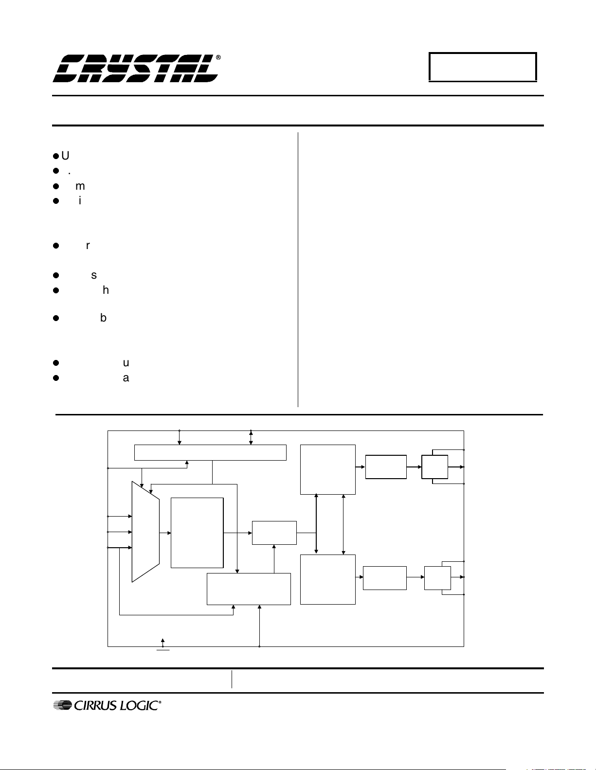
The CS44L10 is a complete stereo digital-to-PWM Class D audio amplifier system controller including interpolation, volume
control, and a headphone amplifier in a 16-pin TSSOP
package.
The CS44L10 architecture uses a direct-to-digital approach
that maintains digital signal integrity to the final output filter.
This minimizes analog interference effects that can negatively
affect system performance.
The CS44L10 contains on-chip digital bass and treble boost,
peak signal limiting, and de-emphasis. The PWM amplifier can
achieve greater than 90% efficiency. This efficiency leads to
longer battery life for portable systems, smaller device package, less heat sink requirements, and smaller power supplies.
The CS44L10 is ideal for portable audio, headphone amplifiers, and mobile phones.
ORDERING INFORMATION
CS44L10-KZ -10 to 70 °C 16-pin TSSOP
SCL/DIF0
Control Port
VL
Digital Volume
SDIN
SCLK
LRCK
Serial
Audio
Port
RST
Control,
Bass/Treble
Boost,
Compression
Limiting,
De-emphasis
Advance Product Information
SDA/DEM
Multibit ∆Σ
Modul ator with
Correction
Interpolation
Multibit ∆Σ
Input Sampling Rate
LRCLK/MCLK Ratio
MCLK
This document contains information for a new product.
Cirrus Logic reserves the right to modify this product without notice.
Modul ator with
Correction
PWM
Conversion
PWM
Conversion
Level
Shifter
Level
Shifter
VA_HPA
HP_A
GND_HPA
VA_HPB
HP_B
GND_HPB
P.O. Box 17847, Austin, Texas 78760
(512) 445 7222 FAX: (512) 445 7581
http://www.cirrus.com
Copyright Cirrus Logic, Inc. 2001
(All Rights Reserved)
MAY ‘01
DS541PP1
1

TABLE OF CONTENTS
1. CHARACTERISTICS AND SPECIFICATIONS ........................................................................ 4
2. TYPICAL CONNECTION DIAGRAMS ...................................................................................10
3. REGISTER QUICK REFERENCE ...................................................................................... 12
4. REGISTER DESCRIPTIONS .................................................................................................. 13
5. PIN DESCRIPTION ................................................................................................................. 25
6. APPLICATIONS ..................................................................................................................... 26
6.1 Grounding and Power Supply Decoupling ...................................................................... 26
6.2 Clock Modes ................................................................................................................... 26
6.3 De-Emphasis .................................................................................................................. 26
6.4 PWM PopGuard Transient Control .................................................................................26
6.5 Recommended Power-up Sequence .............................................................................. 27
6.5.1 Stand Alone Mode ................................................................................................ 27
6.5.2 Control Port Mode ................................................................................................ 27
7. CONTROL PORT INTERFACE ..............................................................................................28
7.1 Two-Wire Format ............................................................................................................ 28
7.1.1 Writing in Two-Wire Format ................................................................................. 28
7.1.2 Reading in Two-Wire Format ............................................................................... 28
7.2 Memory Address Pointer (MAP) ...................................................................................29
7.2.1 INCR (Auto Map Increment Enable) ....................................................................29
7.2.2 MAP3-0 (Memory Address Pointer) ..................................................................... 29
8. PARAMETER DEFINITIONS .................................................................................................. 32
9. PACKAGE DIMENSIONS ....................................................................................................... 33
CS44L10
LIST OF FIGURES
Figure 1. Serial Audio Data Interface Timing .................................................................................. 7
Figure 2. Control Port Timing - Two-Wire Format ...........................................................................9
Figure 3. Typical CS44L10 Connection Diagram Stand-Alone Mode ........................................... 10
Figure 4. Typical CS44L10 Connection Diagram Control Port Mode ............................................ 11
Figure 5. Dynamics Control Block Diagram .................................................................................. 20
Figure 6. De-Emphasis Curve ....................................................................................................... 23
Figure 7. Control Port Timing, Two-Wire Format .......................................................................... 28
Figure 8. Single Speed Stopband Rejection ................................................................................. 30
Figure 9. Single Speed Transition Band........................................................................................ 30
Figure 10. Single Speed Transition Band (Detail) ......................................................................... 30
Figure 11. Single Speed Passband Ripple.................................................................................... 30
Figure 12. Double Speed Stopband Rejection .............................................................................. 30
Contacting Cirrus Logic Support
For a complete listing of Direct Sales, Distributor, and Sales Representative contacts, visit the Cirrus Logic web site at:
http://www.cirrus.com/corporate/contacts/sales.cfm
Preliminary product informati on describes products which are in producti on, but for which full characterization data is not yet available. Advance product information descr ibes products which are in dev elopment and subject to development changes. Ci rrus Logic, Inc. has made best eff orts to ensure that the information
contained in this document is accurate and reliable. However, the information is subject to change without notice and is provided “AS IS” without warranty of
any kind (express or implied). Customers are advised to obtain the latest version of relevant i nformati on to verify, before placing orders, that information being
relied on is current and complete. All products are sold subject to the terms and condi tions of sale supplied at the time of order acknowledgment, includi ng those
pertaini ng to warranty, patent infringement, and limitation of liability. No responsibility is assumed by Cirrus Logic, Inc. for the use of this information, including
use of this information as the basis for manufacture or sale of any items, nor for infri ngements of patents or other rights of third parties. This document is the
property of Cirrus Logic, Inc. and by furnishing thi s information, Cirrus Logic, Inc. grants no license, express or implied under any patents, mask work rights,
copyrights, trademarks, tr ade secrets or other intellectual property rights of Cirrus Logic, Inc. Cirrus Logic, Inc., copyright owner of the information contained
herein, gi ves consent for copies to be made of the informati on only for use within your organization with respect to Cirrus Logic integrated circuits or other parts
of Cirrus Logic, Inc. The same consent is gi ven for similar information contained on any Cirrus Logic website or disk. This consent does not extend to other
copying such as copying for general distribution, advertising or promotional purposes, or for creating any work for resale. The names of products of Cirrus Logic,
Inc. or other vendors and suppliers appearing in this document may be trademarks or service marks of their respective owners which may be register ed in some
jurisdictions. A li st of Cirrus Logi c, Inc. trademarks and service marks can be f ound at http://www.cirrus.com
.
2 DS541PP1

Figure 13. Double Speed Transition Band .................................................................................... 30
Figure 14. Double Speed Transition Band (Detail) ....................................................................... 31
Figure 15. Double Speed Passband Ripple.................................................................................. 31
Figure 16. Left Justified, up to 24-Bit Data....................................................................................31
Figure 17. Right Justified, 24-Bit Data ......................................................................................... 31
Figure 18. I
Figure 19. Right Justified, 16-Bit Data .......................................................................................... 32
2
S, Up to 24-Bit Data ................................................................................................. 31
LIST OF TABLES
Table 1. Register Quick Reference ..............................................................................................12
Table 2. Example Volume Settings .............................................................................................. 15
Table 3. Example Bass Boost Settings ........................................................................................ 15
Table 4. Example Treble Boost Settings ...................................................................................... 15
Table 5. Base Boost Corner Frequencies in Single Speed Mode ................................................ 16
Table 6. Base Boost Corner Frequencies in Double Speed Mode .............................................. 16
Table 7. Treble Boost Corner Frequencies in Single Speed Mode .............................................. 17
Table 8. Example Limiter Attack Rate Settings ............................................................................ 18
Table 9. Example Limiter Release Rate Settings ......................................................................... 18
Table 10. ATAPI Decode ............................................................................................................. 19
Table 11. Single Speed Clock Modes - Control Port Mode .......................................................... 21
Table 12. Single Speed Clock Modes - Stand-Alone Mode ......................................................... 22
Table 13. Double Speed Clock Modes - Control Port Mode ........................................................ 22
Table 14. Double Speed Clock Modes - Stand-Alone Mode ........................................................ 22
Table 15. Digital Interface Format (Stand-Alone Mode) ............................................................... 25
CS44L10
DS541PP1 3
CS44L10
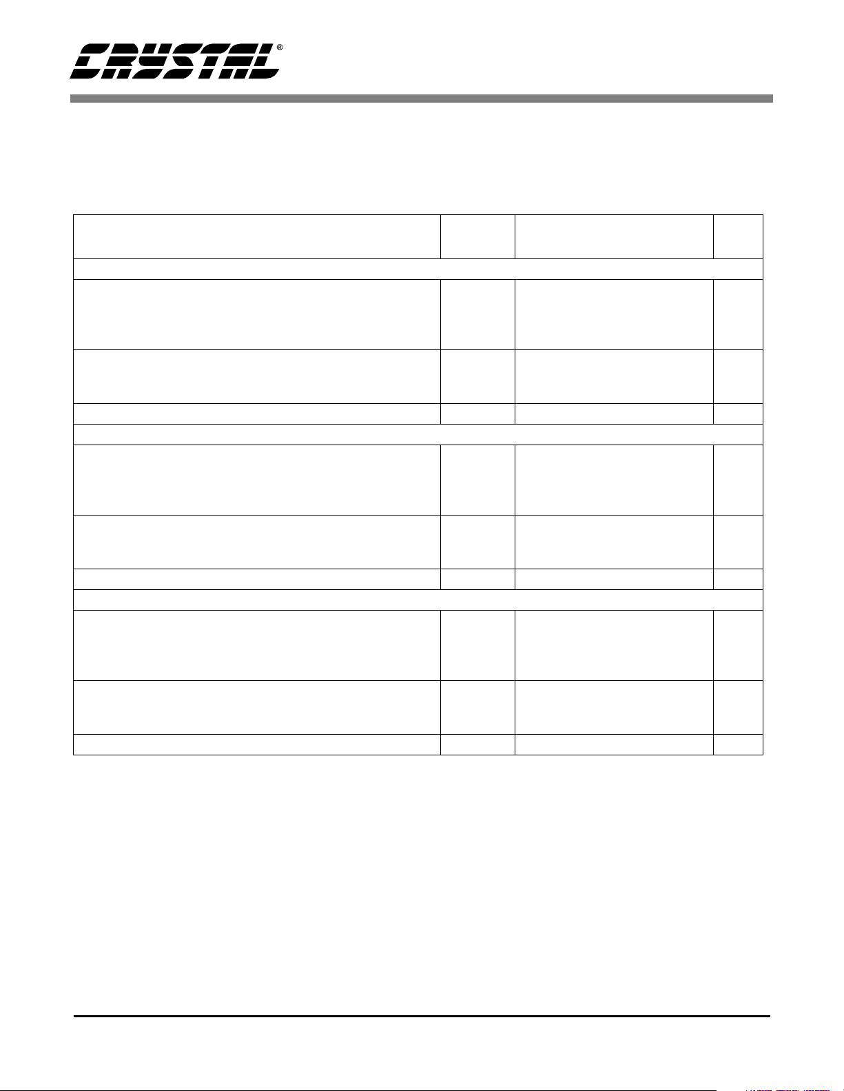
1. CHARACTERISTICS AND SPECIFICATIONS
(TA = 25 °C; GND = 0 V; Logic "1" = VL = 2.4 V; Logic "0" = GND = 0 V; Full-Scale Output Sine Wave, 997 Hz,
MCLK = 12.288 MHz, Measurement Bandwidth 10 Hz to 20 kHz, unless otherwise specified; Fs for Single Speed
Mode = 48 kHz, SCLK = 3.072 MHz; Fs for Double Speed Mode = 96 kHz, SCLK = 6.144 MHz. Test load
R
=16Ω, CL = 10pF.) (See Typical CS44L10 Connection Diagram.)
L
Parameter Symbol Min Typ Max Unit
Headphone Output Dynamic Performance for VD = VL = VA_HPx = 2.4 V
Dynamic Range 18 to 24-Bit A-Weighted
UnWeighted
16-Bit A-Weighted
Unweighted
Total Harmonic Distortion + Noise 0 dBFS
THD+N -
-20 dBFS
-60 dBFS
Interchannel Isolation (1 kHz)
Headphone Output Dynamic Performance for VD = VL = VA_HPx = 3.0 V
Dynamic Range 18 to 24-Bit A-Weighted
UnWeighted
16-Bit A-Weighted
Unweighted
Total Harmonic Distortion + Noise 0 dB
THD+N -
-20 dB
-60 dB
Interchannel Isolation (1 kHz)
Headphone Output Dynamic Performance for VD = VL = VA_HPx = 5.0 V
Dynamic Range 18 to 24-Bit A-Weighted
UnWeighted
16-Bit A-Weighted
Unweighted
Total Harmonic Distortion + Noise 0 dB
THD+N -
-20 dB
-60 dB
Interchannel Isolation (1 kHz)
TBD
TBD
-
-
-
-
93
91
91
89
-62
-71
-31
-
-
-
-
TBD
-
-
dB
dB
dB
dB
dB
dB
dB
-TBD-dB
TBD
TBD
-
-
-
-
95
92
92
90
-64
-72
-32
-
-
-
-
TBD
-
-
dB
dB
dB
dB
dB
dB
dB
-TBD-dB
TBD
TBD
-
-
-
-
99
96
91
93
-67
-76
-36
-
-
-
-
TBD
-
-
dB
dB
dB
dB
dB
dB
dB
-TBD-dB
4 DS541PP1

CHARACTERISTICS AND SPECIFICATIONS (Continued)
Parameters Symbol Min Typ Max Units
PWM Headphone Output
Full Scale Headphone Output Voltage
Headphone Output Quiescent Voltage
Interchannel Gain Mismatch
Modulation Index
Maximum Headphone Output VA_HPx= 2. 4V
AC-Current VA_H P x=5.0V
Parameter
Symbol Min Typ Max Min Typ Max Unit
Digital Filter Response (Note 1))
Passband to -0.05 dB corner
(Note 2) to -0.1 dB corner
to -3 dB corner
Frequency Response 10 Hz to 20 kHz
(Note 3)
StopBand
StopBand Attenuation (Note 4)
Group Delay
Passband Group Delay Deviation 0 - 40 kHz
tgd - 9/Fs - - 4/Fs - s
.5465 - - .577 - - Fs
0 - 20 kHz
De-emphasis Error Fs = 32 kHz
(Relative to 1 kHz) Fs = 44.1 kHz
Fs = 48 kHz
I
HP
Single Speed Mode Double Speed Mode
0
-
0
-.02 - +.08 0 - +0.11 dB
50 - - 55 - - dB
-
--±0.36/Fs
-
-
-
TBD 0.85 x VA_HP TBD Vp
-0.5 x VA_HP- VDC
-0.1-dB
--85%
-
-
-
.4535
-
-
-
-
-
.4998
+.2/-.1
+.05/-.14
+0/-.22
CS44L10
45
80
-
-
0
0
-
-
--±1.39/Fs
±0.23/Fs--
(Note 5)
-
-
-
-
-
.4426
.4984
mA
mA
Fs
Fs
Fs
s
s
dB
dB
dB
Note:
1. Filter response is not tested but is guaranteed by design.
2. Response is clock dependent and will scale with Fs. Note that the response plots (Figures 8-15) have
been normalized to Fs and can be de-normalized by multiplying the X-axis scale by Fs.
3. Referenced to a 1 kHz, full-scale sine wave.
4. For Single Speed Mode, the measurement bandwidth is 0.5465 Fs to 3 Fs.
For Double Speed Mode, the measurement bandwidth is 0.577 Fs to 1.4 Fs.
5. De-emphasis is not available in double speed mode.
DS541PP1 5
CS44L10
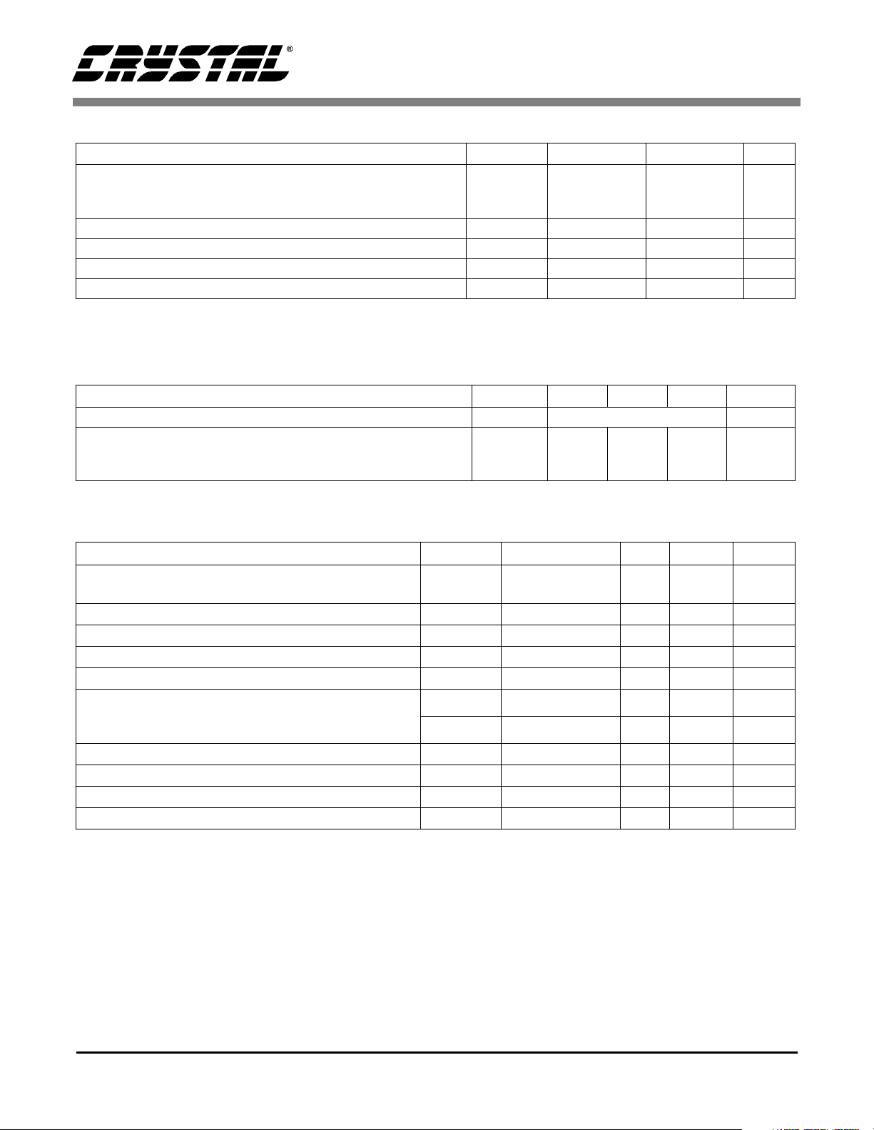
ABSOLUTE MAXIMUM RATINGS (GND = 0V; all voltages with respect to ground.)
Parameters Symbol Min Max Units
DC Power Supplies: Headphone
Interface
Digital
Input Current, Any Pin Except Supplies
Digital Input Voltage
Ambient Operating Temperature (power applied)
Storage Temperature
CAUTION: Operation at or beyond these limits may result in permanent damage to the device. Normal operation
is not guaranteed at these extremes.
RECOMMENDED OPERATING CONDITIONS (GND = 0V; all voltages with respect to ground.)
Parameters Symbol Min Typ Max Units
Ambient Temperature
DC Power Supplies: Headphone
Interface
Digital
VA_H P x
VL
VD
I
in
V
IND
T
A
T
stg
T
A
VA_H Px
VL
VD
2.4
2.4
2.4
5.5
5.5
5.5
±10 mA
-0.3 VL + 0.4 V
-55 125 °C
-65 150 °C
-10 - 70 °C
2.4
2.4
2.4
-
-
-
5.0
5.0
5.0
V
V
V
V
V
V
SWITCHING CHARACTERISTICS (T
Logic 1 = VL, CL = 20pF)
Parameters Symbol Min Typ Max Units
Input Sample Rate Single Speed Mode
Double Speed Mode
MCLK Duty Cycle
LRCK Duty Cycle
SCLK Pulse Width Low
SCLK Pulse Width High
SCLK Period Single Speed Mode
Double Speed Mode
SCLK rising to LRCK edge delay
SCLK rising to LRCK edge setup time
SDIN valid to SCLK rising setup time
SCLK rising to SDIN hold time
= -10 to 70°C; VL = 2.4V - 5.0V; Inputs: Logic 0 = GND,
A
Fs
Fs
8
50
-
-
50
100
40 50 60 %
40 50 60 %
t
sclkl
t
sclkh
t
sclkw
t
sclkw
t
slrd
t
slrs
t
sdlrs
t
sdh
20 - - ns
20 - - ns
1
---------------------128()Fs
1
------------------64()Fs
--ns
--ns
20 - - ns
20 - - ns
20 - - ns
20 - - ns
kHz
kHz
6 DS541PP1
CS44L10
LRCK
t
slrs
SCLK
SDATA
t
slrd
t
sclkw
t
sdlrs
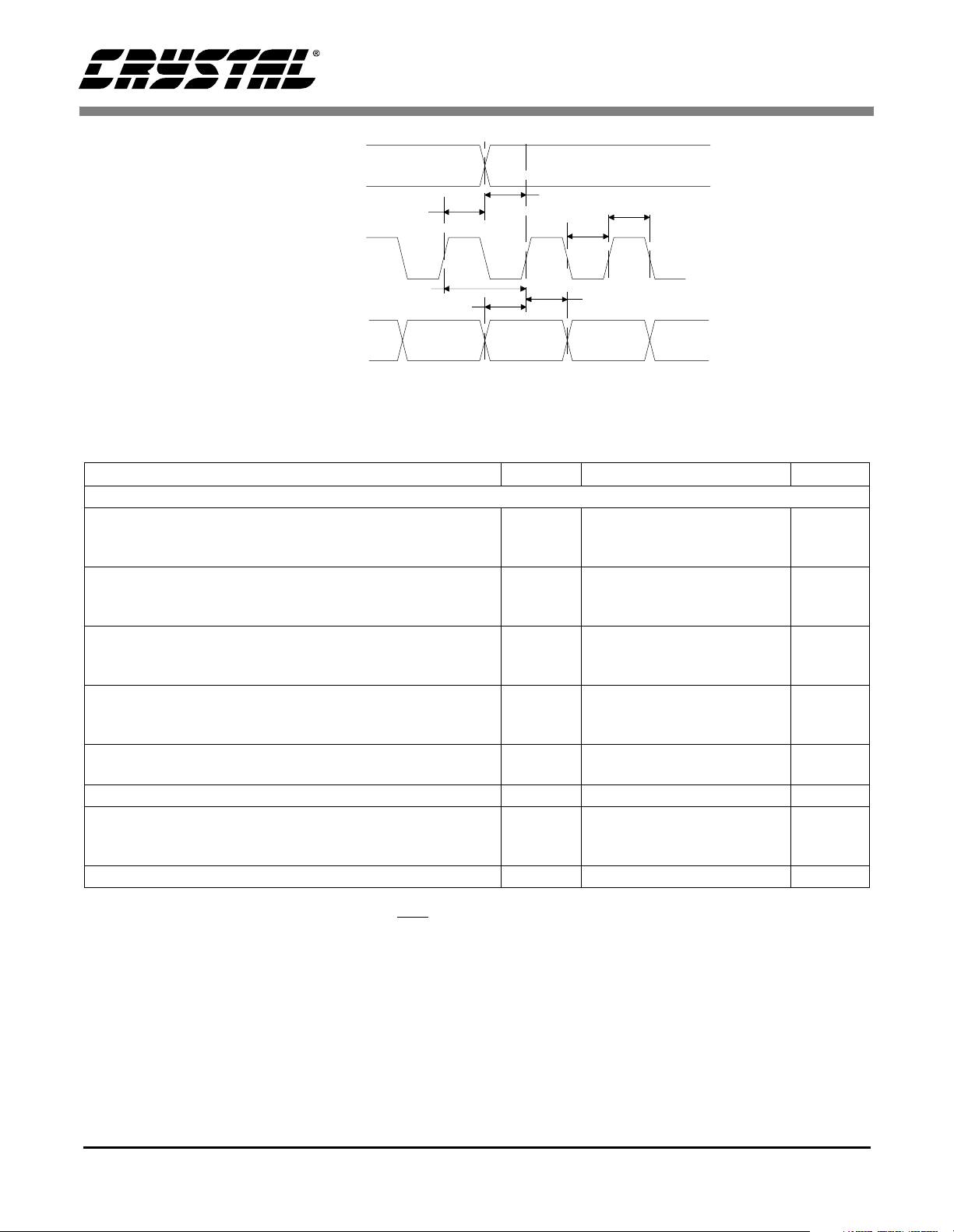
Figure 1. Serial Audio Data Interface Timing
POWER AND THERMAL CHARACTERISTICS (GND = 0 V; All voltages with respect to
ground. All measurements taken with all zeros input and open outputs, unless otherwise specified.)
Parameters Symbol Min Typ Max Units
Power Supplies
Power Supply Current- VA_HPx= 2.4 V
Normal Operation VD = 2.4 V
VL= 2.4 V
Power Supply Current- VA_HPx = 2.4V
Power Down Mode (Note 6) VD = 2.4V
VL = 2.4V
Power Supply Current- VA_HPx = 5.0 V
Normal Operation VD = 5.0 V
VL = 5.0 V
Power Supply Current- VA_HPx = 5.0V
Power Down Mode (Note 6) VD = 5.0V
VL = 5.0 V
Total Power Dissipation- All Supplies = 2.4 V
Normal Operation All Supplies = 5.0 V
Power Supply Rejection Ratio
Maximum Headphone Power Dissipation
(1 kHz full-scale sine wave
into 16 ohm load) VA=5 . 0 V
Package Thermal Resistance
VA=2 . 4 V
Note:
6. Power Down Mode is defined as RST
= LO with all clocks and data lines held static.
I
VA_ HP
I
D
I
L
I
VA_ HP
I
D
I
L
I
VA_ HP
I
D
I
L
I
VA_ HP
I
D
I
L
PSRR - 0 - dB
θ
JA
t
sclkh
t
sclkl
t
sdh
-
-
-
-
-
-
-
-
-
-
-
-
-
-
-
-
-
1
10
1
TBD
TBD
TBD
2
20
2
TBD
TBD
TBD
29
120
-
23
100
-
-
-
-
-
-
-
-
-
-
-
-
-
-
-
-
-
-75-°C/Watt
mA
mA
mA
µA
µA
µA
mA
mA
mA
µA
µA
µA
mW
mW
mW
mW
DS541PP1 7
CS44L10
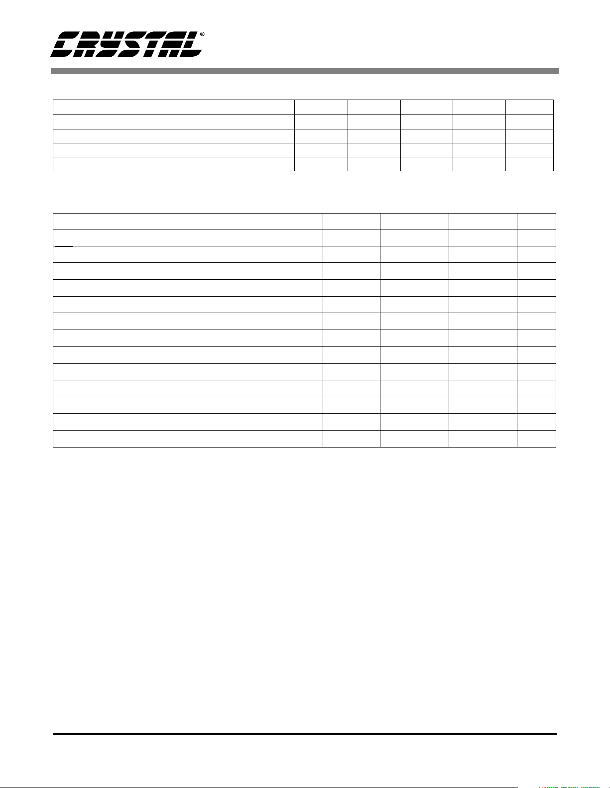
DIGITAL CHARACTERISTICS (T
= 25° C; VL = 2.4V - 3.6V; GND=0V)
A
Parameters Symbol Min Typ Max Units
High-Level Input Voltage
Low-Level Input Voltage
Input Leakage Current
Input Capacitance
V
IH
V
IL
I
in
0.7 x VL - - V
--0.3 x VLV
--±10µA
-8-pF
SWITCHING CHARACTERISTICS- CONTROL PORT- TWO-WIRE FORMAT
(Note 7) (T
SCL Clock Frequency
RST Rising Edge to Start
Bus Free Time Between Transmissions
Start Condition Hold Time (prior to first clock pulse)
Clock Low time
Clock High Time
Setup Time for Repeated Start Condition
SDA Hold Time from SCL Falling (Note 8)
SDA Setup time to SCL Rising
Rise Time of SCL and SDA
Fall Time SCL and SDA
Setup Time for Stop Condition
Acknowledge Delay from SCL Falling (Note 9)
=25° C; VL = 2.4 V - 5.0 V; Inputs: Logic 0 = GND, Logic 1 = VL, CL=30pF)
A
Parameter Symbol Min Max Unit
f
scl
t
irs
t
buf
t
hdst
t
low
t
high
t
sust
t
hdd
t
sud
trc, t
tfc, t
t
susp
t
ack
rc
fc
- 100 kHz
500 - ns
4.7 - µs
4.0 - µs
4.7 - µs
4.0 - µs
4.7 - µs
0-µs
250 - ns
-1µs
- 300 ns
4.7 - µs
- (Note 10) ns
Note:
2
7. The Two-Wire Format is compatible with the I
8. Data must be held for sufficient time to bridge the transition time, t
C protocol.
, of SCL.
fc
9. The acknowledge delay is based on MCLK and can limit the maximum transaction speed.
5
---------------------
10. for Single-Speed Mode and for Double-Speed Mode.
256 Fs×
5
--------------------128 F s×
8 DS541PP1
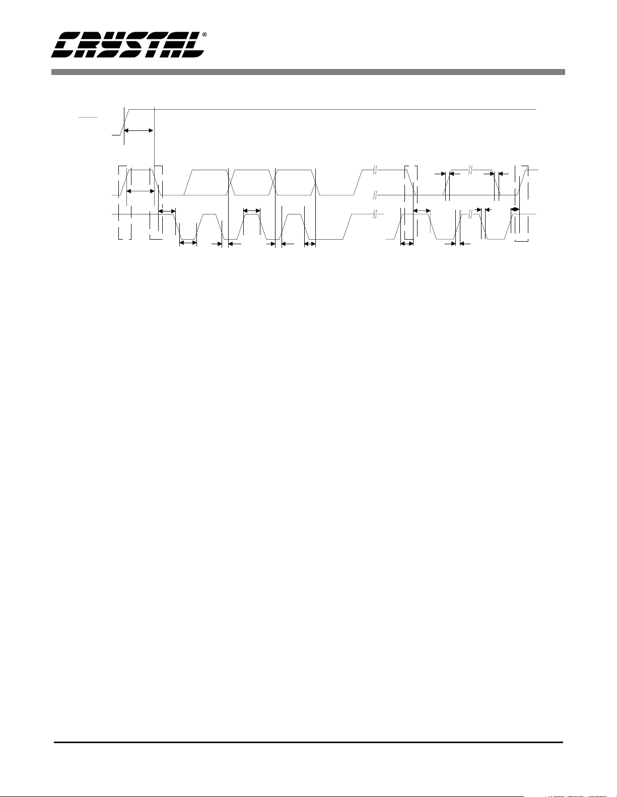
RST
SDA
SCL
t
irs
Stop S t a rt
t
buf
t
hdst
CS44L10
Repeated
Start
t
rd
t
high
t
hdst
t
fc
Stop
t
fd
t
susp
t
low
t
hdd
t
sud
t
ack
Figure 2. Control Port Timing - Two-Wire Format
t
sust
t
rc
DS541PP1 9
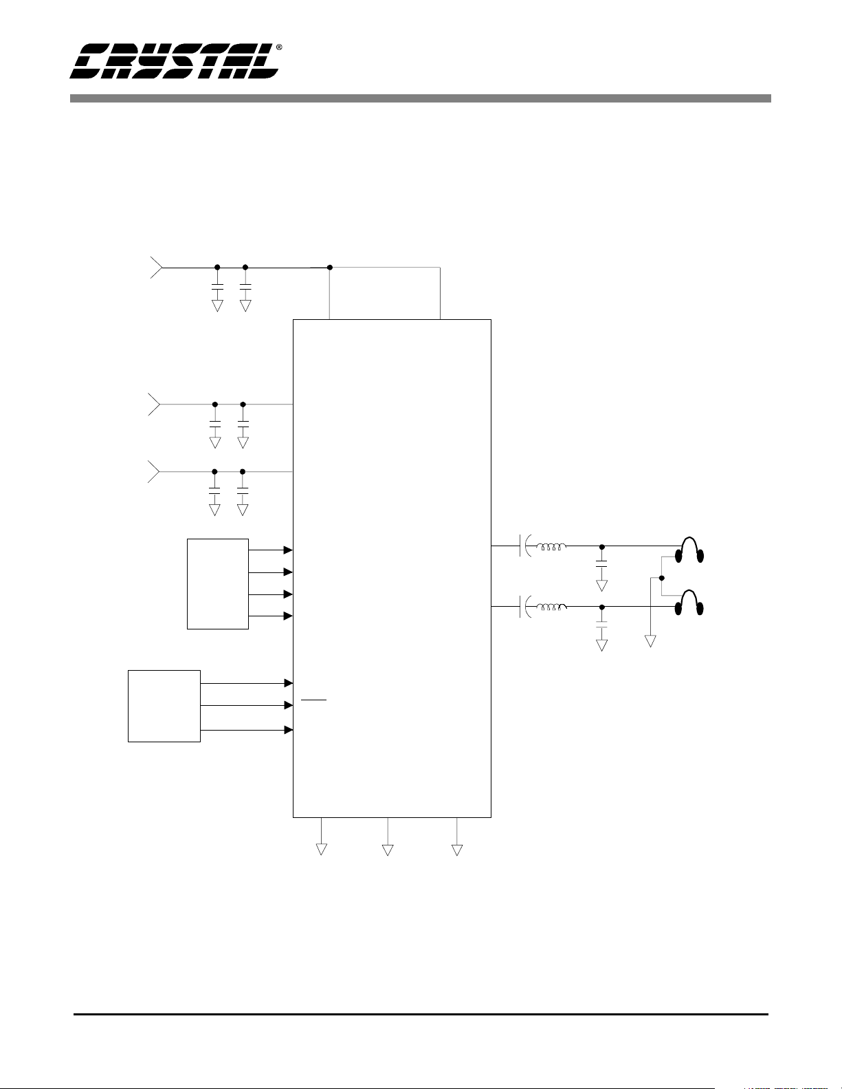
2. TYPICAL CONNECTION DIAGRAMS
2.4 to 5.0 V
Supply
100 µF
+
0.1 µ
F
12 13
VA_HPA
CS44L10
VA_HPB
2.4 to 5.0 V
Supply
2.4 to 5.0 V
Supply
1.0 µF
1.0 µF
Mode
Control
+
+
Digi tal
A
udio
Source
0.1 µF
5
0.1 µF
4
2
3
1
9
16
7
VL
VD
CS44L10
Cout
+
Cout
+
100 µH
100 µH
0.15
µF
0.15
µF
Ω
16
Headphone s
MCLK
LRCK
SCLK
SDIN
DEM
RST
8
DIF 0
HP_A
HP_B
11
220 µ F
14
220 µ F
GNDGNDGND
10
15
6
Figure 3. Typical CS44L10 Connection Diagram Stand-Alone Mode
10 DS541PP1
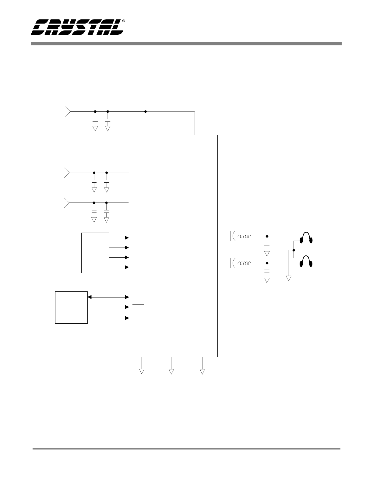
2.4 to 5.0 V
Supply
100 µF
CS44L10
+
0.1 µ
F
12 13
VA_HPA
VA_HPB
2.4to5.0V
Supply
2.4 to 5.0 V
Supply
1.0 µF
1.0 µ F
µC/
Mode
Control
+
+
Digital
A
udio
Source
7
0.1 µF
5
0.1 µF
4
2
3
1
9
16
8
VL
VD
MCLK
LRCK
SCLK
SDIN
SDA
RST
SCL
CS44L10
HP_A
HP_B
Cout
11
+
220 µ F
Cout
14
+
220 µF
100 µH
100 µH
0.15
µF
0.15
µF
Ω
16
Headphones
G
NDGNDGND
10
15
6
Figure 4. Typical CS44L10 Connection Diagram Control Port Mode
DS541PP1 11
 Loading...