

Page 1
Features
CS44600
6-Channel Digital Amplifier Controller
> 100 dB Dynamic Range - System Level
< 0.03% THD+N @ 1 W - System Level
32 kHz to 192 kHz Sample Rates
Internal Oscillator Circuit Supports 24.576 MHz
to 54 MHz Crystals
Integrated Sample Rate Converter (SRC)
– Eliminates Clock Jitter Effects
– Input Sample Rate Independent Operation
Power Supply Rejection Realtime Feedback
Spread Spectrum Modulation - Reduces EMI
PWM Popguard
®
for Single-Ended Mode
PS_SYNC
Control
Auto Fs
Detect
DAI
Serial
Port
PWM
Clock
Volume
/ Limiter
Volume
/ Limiter
SRC
Volume
/ Limiter
XTI
XTO
SYS_CLK
DAI_MCLK
DAI_SCLK
DAI_LRCK
DAI_SDIN1
DAI_SDIN2
DAI_SDIN3
XTAL
Eliminates AM Frequency Interference
Programmable Load Compensation Filters
Support for up to 40 kHz Audio Bandwidth
Digital Volume Control with Soft Ramp
– +24 to -127 dB in 0.25 dB Steps
Per Channel Programmable Peak Detect and
Limiter
SPI™ and I²C
Separate 2.5 V to 5.0 V Serial Port and Host
®
Host Control Interfaces
Control Port Supplies
PSR_RESET
PSR_EN
PSR_MCLK
PSR_SYNC
PSR_DATA
PWMOUTA1+
PWMOUTA1PWMOUTB1+
PWMOUTB1-
PWMOUTA2+
PWMOUTA2PWMOUTB2+
PWMOUTB2-
PWMOUTA3+
PWMOUTA3PWMOUTB3+
PWMOUTB3-
Multibit
Σ∆
Modulator
Multibit
Σ∆
Modulator
Multibit
Σ∆
Modulator
Power
Supply
Rejection
PWM
Conversion
PWM
Conversion
PWM
Conversion
MUTE
SCL/CCLK
SDA/CDOUT
AD1/CDIN
AD0/CS
RST
INT
http://www.cirrus.com
SPI/I2C Host
Control Port
Copyright © Cirrus Logic, Inc. 2006
(All Rights Reserved)
PWM
Backend
Control/
Status
GPIO0
GPIO1
GPIO2
GPIO3
GPIO4
GPIO5
GPIO6
MARCH '06
DS633F1
Page 2

CS44600
General Description
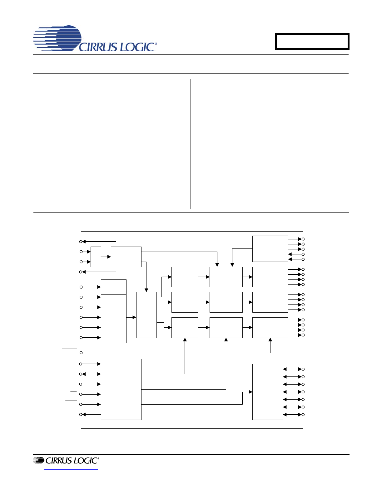
The CS44600 is a multi-channel digital-to-PWM Class D audio system controller including interpolation, sample rate
conversion, half- and full-bridge PWM driver outputs, and power supply rejection feedback in a 64-pin LQFP package.The architecture uses a direct-to-digital approach that maintains digital signal integrity to the final output filter,
minimizing analog interference effects which negatively affect system performance.
The CS44600 integrates on-chip digital volume control, peak detect with limiter, de-emphasis, and 7 GPIO’s, allowing easy interfacing to many commonly available power stages. The PWM amplifier can achieve greater than 90%
efficiency. This efficiency provides for smalle r device package, less heat sink requirements, and smaller power
supplies.
The CS44600 is ideal for audio systems requiring wide dynamic range, negligible distortion an d low noise, such as
A/V receivers, DVD receivers, digital speaker and automotive audio systems.
2 DS633F1
Page 3

TABLE OF CONTENTS
1. CHARACTERISTICS AND SPECIFICATIONS ...................................................................................... 8
SPECIFIED OPERATING CONDITIONS ..............................................................................................8
ABSOLUTE MAXIMUM RATINGS ........................................................................................................ 8
DC ELECTRICAL CHARACTERISTICS .......................................... ... ... .... ... ... ... .... ... ... ... ... .... .............. 9
DIGITAL INTERFACE CHARACTERISTICS ........................................................................................ 9
PWM OUTPUT PERFORMANCE CHARACTERISTICS .................................................................... 10
PWM FILTER CHARACTERISTICS ................................................................................................... 11
SWITCHING CHARACTERISTICS - XTI ............................................................................................ 11
SWITCHING CHARACTERISTICS - SYS_CLK .................................................................................. 12
SWITCHING CHARACTERISTICS - PWMOUTA1-B3 ....................................................................... 12
SWITCHING CHARACTERISTICS - PS_SYNC ................................................................................. 12
SWITCHING CHARACTERISTICS - DAI INTERFACE ...................................................................... 13
SWITCHING CHARACTERISTICS - CONTROL PORT - I²C FORMAT ............................................. 14
SWITCHING CHARACTERISTICS - CONTROL PORT - SPI FORMAT ............................................ 15
2. PIN DESCRIPTIONS ......................................................................................................................... 16
2.1 I/O Pin Characteristics ................................................................................................................ 19
3. TYPICAL CONNECTION DIAGRAMS ......................................................................................20
4. APPLICATIONS ................................................................................................................................... 22
4.1 Overview ................................................................................................. ... ... .... ... ... ...................... 22
4.2 Feature Set Summary ................................................................................................................... 22
4.3 Clock Generation .... ................................................. ... ................................................ ................... 23
4.3.1 FsIn Domain Clocking .......................................................................................................... 24
4.3.2 FsOut Domain Clocking ........................... ... .... ... ... ................................................ .... ... ... ...... 24
4.4 FsIn Clock Domain Modules ......................................................................................................... 26
4.4.1 Digital Audio Input Port .. .... ................................................ ... ... .... ... ...................................... 26
4.4.2 Auto Rate Detect ............................................ ... ................................................................... 30
4.4.3 De-Emphasis ................. ................................................. ... ................................................... 30
4.5 FsOut Clock Domain Modules .......................................................................................................31
4.5.1 Sample Rate Converter .............. ... .... ... ... ... ................................................. ... ... ... .... ............ 31
4.5.2 Load Compensation Filter .................................................................................................... 31
4.5.3 Digital Volume and Mute Control .......................................... ... .... ... ... ... .... ............................31
4.5.4 Peak Detect / Limiter ............................................................................................................ 32
4.5.5 PWM Engines ....... ... ................................................ .... ... ... ... ................................................ 32
4.5.6 Interpolation Filter ....................................... .... ... ... ... ............................................................. 33
4.5.7 Quantizer ................. ... ................................................. ... ...................................................... 33
4.5.8 Modulator ................................................ ... .... ... ... ................................................ ................ 33
4.5.9 PWM Outputs ................................................. ... ... ... .... ... ... ................................................... 33
4.5.10 Power Supply Rejection (PSR) Real-Time Feedback ........................................................ 34
4.6 Control Port Description and Timing ...... .... ................................................................................... 35
4.6.1 SPI Mode ....... ................................................. ... ................................................ ... ................ 35
4.6.2 I²C Mode .. ... ... ... .... ... ... ... .... ................................................ ... ................................................ 36
4.6.3 GPIOs ............................................ .... ... ... ... .... ... ... ............................................. ...................37
4.6.4 Host Interrupt ........................................ ... ... .............................................. ... ... ... ... ................ 37
5. POWER SUPPLY, GROUNDING, AND PCB LAYOUT ....................................................................... 38
5.1 Reset and Power-Up .....................................................................................................................41
5.1.1 PWM PopGuard® Transient Control .................................................................................... 41
5.1.2 Recommended Power-Up Sequence ................................................................................... 41
5.1.3 Recommended PSR Calibration Sequence .................. ... ... ... .... ... ... ... .... ... ... ...................... 42
5.1.4 Recommended Power-Down Sequence .............................................................................. 43
6. REGISTER QUICK REFERENCE ........................................................................................................ 44
7. REGISTER DESCRIPTION .................................................................................................................. 48
7.1 Memory Address Pointer (MAP) .......................... ............................. ............................. ................ 48
CS44600
DS633F1 3
Page 4

CS44600
7.1.1 Increment (INCR) ................................................................................................................. 48
7.1.2 Memory Address Pointer (MAPx) ......................................................................................... 48
7.2 CS44600 I.D. and Revision Register (address 01h) (Read Only) ................................................. 48
7.2.1 Chip I.D. (Chip_IDx) ............................................................................................................. 48
7.2.2 Chip Revision (Rev_IDx) ...................................................................................................... 49
7.3 Clock Configuration and Power Control (address 02h) ................................................................. 50
7.3.1 Enable SYS_CLK Output (EN_SYS_CLK) ........................................................................... 50
7.3.2 SYS_CLK Clock Divider Settings (SYS_CLK_DIV[1:0]) ....................................................... 50
7.3.3 PWM Master Clock Divider Settings (PWM_MCLK_DIV[1:0]) ............................................. 50
7.3.4 Power Down XTAL (PDN_XTAL) ......................................................................................... 50
7.3.5 Power Down Output Mode (PDN_OUTPUT_MODE) ..................... ................................... ... 51
7.3.6 Power Down (PDN) .............................................................................................................. 51
7.4 PWM Channel Power Down Control (address 03h) ...................................................................... 51
7.4.1 Power Down PWM Channels (PDN_PWMB3:PDN_PWMA1) ............................................. 51
7.5 Misc. Configuration (address 04h) ................................................................................................ 52
7.5.1 Digital Interface Format (DIFX) ....................... ... ... ... .... ... ................................................ ...... 52
7.5.2 AM Frequency Hopping (AM_FREQ_HOP) ......................................................................... 52
7.5.3 Freeze Controls (FREEZE) .................................................................................................. 52
7.5.4 De-Emphasis Control (DEM[1:0]) ......................................................................................... 53
7.6 Ramp Configuration (address 05h) ............................................................................................... 53
7.6.1 Ramp-Up/Down Setting (RAMP[1:0]) .................................................................................. 53
7.6.2 Ramp Speed (RAMP_SPD[1:0]) .......................... ... .... ... ... ... ... .... ... ... ... .... ... ... ... ... .... ... ... ... ... 53
7.7 Volume Control Configuration (address 06h) ............................................................. ... .... ... ... ... ... 54
7.7.1 Single Volume Control (SNGVOL) ....................................................................................... 54
7.7.2 Soft Ramp and Zero Cross Control (SZC[1:0]) .................. ... ... .... ... ... ... .... ... ......................... 54
7.7.3 Enable 50% Duty Cycle for Mute Condition (MUTE_50/50) ................................................. 54
7.7.4 Soft Ramp-Down on Interface Error (SRD_ERR) ............................. ....... ...... ...... ....... ...... ... 55
7.7.5 Soft Ramp-Up on Recovered Interface Error (SRU_ERR) ................................................... 55
7.7.6 Auto-Mute (AMUTE) ............................................................................................................. 55
7.8 Master Volume Control - Integer (address 07h) ............................................................................ 56
7.8.1 Master Volume Control - Integer (MSTR_IVOL[7:0]) ............................................................ 56
7.9 Master Volume Control - Fraction (address 08h) .......................................................................... 56
7.9.1 Master Volume Control - Fraction (MSTR_FVOL[1:0]) ......................................................... 56
7.10 Channel XX Volume Control - Integer (addresses 09h - 0Eh) .................................................... 58
7.10.1 Channel Volume Control - Integer (CHXx_IVOL[7:0]) ..................... ................................... 58
7.11 Channel XX Volume Control1 - Fraction (address 11h) ............................................................ 58
7.12 Channel XX Volume Control2 - Fraction (address 12h) .............................................................. 58
7.12.1 Channel Volume Control - Fraction (CHXX_FVOL[1:0]) .................................................... 58
7.13 Channel Mute (address 13h) ....................................................................................................... 59
7.13.1 Independent Channel Mute (CHXX_MUTE) ....................................................................... 59
7.14 Channel Invert (address 14h) ...................... ....................................................... ......................... 59
7.14.1 Invert Signal Polarity (CHXX_INV) ......................................................... ... ... ... ... .... ... ... ... ... 59
7.15 Peak Limiter Control Register (address 15h) ............................................................................. 60
7.15.1 Peak Signal Limit All Channels (LIMIT_ALL) ...................................................................... 60
7.15.2 Peak Signal Limiter Enable (LIMIT_EN) .......... ... ... .... ... ... ... ... .... ... ... ... .... ... ... ... ... .... ............ 60
7.16 Limiter Attack Rate (address 16h) .............................................................................................. 60
7.16.1 Attack Rate (ARATE[7:0]) .................................................................................................. 60
7.17 Limiter Release Rate (address 17h) ....................................................................................
7.17.1 Release Rate (RRATE[7:0]) ...............................................................................................61
7.18 Chnl XX Load Compensation Filter - Coarse Adjust (addresses 18h, 1Ah, 1Ch, 1Eh, 20h, 22h) ..
61
7.18.1 Channel Compensation Filter - Coarse Adjust (CHXX_CORS[5:0]) .................................. 61
7.19 Chnl XX Load Compensation Filter - Fine Adjust (addresses 19h, 1Bh, 1Dh, 1Fh, 21h, 23h) .... 62
7.19.1 Channel Compensation Filter - Fine Adjust (CHXX_FINE[5:0]) ......................................... 62
..... 61
4 DS633F1
Page 5

CS44600
7.20 Interrupt Mode Control (address 28h) ......................................................................................... 62
7.20.1 Interrupt Pin Control (INT1/INT0) .......................................................................................62
7.20.2 Overflow Level/Edge Select (OVFL_L/E) ........................................................................... 63
7.21 Interrupt Mask (address 29h) ...................................................................................................... 63
7.22 Interrupt Status (address 2Ah) (Read Only) ...............................................................................63
7.22.1 SRC Unlock Interrupt (SRC_UNLOCK) ................. .... ... ................................................ ... ... 63
7.22.2 SRC Lock Interrupt (SRC_LOCK) ...................................................................................... 64
7.22.3 Ramp-Up Complete Interrupt (RMPUP_DONE) ................................................................. 64
7.22.4 Ramp-Down Complete Interrupt (RMPDN_DONE) ......................... ... .... ... ... ... ... .... ... ......... 64
7.22.5 Mute Complete Interrupt (Mute_DONE) ............. ................................................................ 64
7.22.6 Channel Over Flow Interrupt (OVFL_INT) ....................................................................... ... 64
7.22.7 GPIO Interrupt Condition (GPIO_INT) ....................................................................... ... ......64
7.23 Channel Over Flow Status (address 2Bh) (Read Only) .............................................................. 65
7.23.1 ChXX_OVFL ....................................................................................................................... 65
7.24 GPIO Pin In/Out (address 2Ch) ................................................................................................... 65
7.24.1 GPIO In/Out Selection (GPIOX_I/O) .................................................................................. 65
7.25 GPIO Pin Polarity/Type (address 2Dh) .................................... ... ... ............................................. 65
7.25.1 GPIO Polarity/Type Selection (GPIOX_P/T) ...................................................................... 65
7.26 GPIO Pin Level/Edge Trigger (address 2Eh) .............................................................................. 66
7.26.1 GPIO Level/Edge Input Sensitive (GPIOX_L/E) ................................................................. 66
7.27 GPIO Status Register (address 2Fh) .......................................................................................... 66
7.27.1 GPIO Pin Status (GPIOX_STATUS) .................................................................................. 66
7.28 GPIO Interrupt Mask Register (address 30h) ........ ... ... ... .... ... ... ... ... .... ... ...................................... 67
7.28.1 GPIO Pin Interrupt Mask (M_GPIOX) ................................................................................. 67
7.29 PWM Configuration Register (address 31h) ...............................................................................67
7.29.1 Over Sample Rate Selection (OSRATE) ............................................................................ 67
7.29.2 Channels A1 and B1 Output Configuration (A1/B1_OUT_CNFG) .. ... .... ... ... ... ... .... ... ... ... ... 67
7.29.3 Channels A2 and B2 Output Configuration (A2/B2_OUT_CNFG) .. ... .... ... ... ... ... .... ... ... ... ... 67
7.29.4 Channel A3 Output Configuration (A3_OUT_CNFG) ......................................................... 68
7.29.5 Channel B3 Output Configuration (B3_OUT_CNFG) ......................................................... 68
7.30 PWM Minimum Pulse Width Register (address 32h) ................................................................. 68
7.30.1 Disable PWMOUTXX - Signal (DISABLE_PWMOUTXX-) ................................................. 68
7.30.2 Minimum PWM Output Pulse Settings (MIN_PULSE[4:0]) . ................................................ 68
7.31 PWMOUT Delay Register (address 33h) ................................................................................... 69
7.31.1 Differential Signal Delay (DIFF_DLY[2:0]) .......................... ....................................... ......... 69
7.31.2 Channel Delay Settings (CHNL_DLY[4:0]) ..................... ................................ ................... 69
7.32 PSR and Power Supply Configuration (address 34h) ................................................................. 70
7.32.1 Power Supply Rejection Enable (PSR_EN) ................................................. ... ... .... ... .........70
7.32.2 Power Supply Rejection Reset (PSR_RESET) .................................................................. 70
7.32.3 Power Supply Rejection Feedback Enable (FEEDBACK_EN) .................. ... ...... ....... ...... ... 71
7.32.4 Power Supply Sync Clock Divider Settings (PS_SYNC_DIV[2:0]) ............ .........................71
7.33 Decimator Shift/Scale (addresses 35h, 36h, 37h) ................. ...................................................... 71
7.33.1 Decimator Shift (DEC_SHIFT[2:0]) ..................................................................................... 71
7.33.2 Decimator Scale (DEC_SCALE[18:0]) ............................................................................... 71
7.34 Decimator Outd (addresses 3Bh, 3Ch, 3Dh) ............................................................................... 72
7.34.1 Decimator Outd (DEC_OUTD[23:0]) .................................................................................. 72
8. PARAMETER DEFINITIONS ................................................................................................................ 73
9. REFERENCES ...................................................................................................................................... 75
10. PACKAGE DIMENSIONS ......................................................................................................... 76
11. THERMAL CHARACTERISTICS ................................. ... ... ... ................................................. ... ... ...... 77
12. ORDERING INFORMATION . ... ... .... ... ................................................ ... .... ... ... ... .... ... ... ... ................... 77
13. REVISION HISTORY .................................................................... ... ... ... ............................................. 77
DS633F1 5
Page 6

LIST OF FIGURES
Figure 1.Performance Characteristics Evaluation Active Filter Circuit ...................................................... 10
Figure 2.XTI Timings .......................................... .... ... ... ... .... ...................................................................... 11
Figure 3.SYS_CLK Timings ...................................................................................................................... 12
Figure 4.PWMOUTxx Timings ........... ................................................. ... ... ... .... ... ... ... .... ... ......................... 12
Figure 5.PS_SYNC Timings ...................... ... ... ... .... ... ... ... .... ... ... ................................................................ 12
Figure 6.Serial Audio Interface Timing ... ... ... ... .................................................... ... ... .... ... ... ...................... 13
Figure 7.Serial Audio Interface Timing - TDM Mode ................................................................................. 13
Figure 8.Control Port Timing - I²C Format ........................................................................ ... ... ... .... ............ 14
Figure 9.Control Port Timing - SPI Format ............................. ... ... .... ... ... ... ................................................ 15
Figure 10.CS44600 Pinout Diagram ...................................................... ... ... .... ... ... ... .... ............................ 16
Figure 11.Typical Full-Bridge Connection Diagram ............ ... ... ... .... ... ... ... ... ............................................. 20
Figure 12.Typical Half-Bridge Connection Diagram ..................................................................................21
Figure 13.CS44600 Data Flow Diagram (Single Channel Shown) ...........................................................23
Figure 14.Fundamental Mode Crystal Configuration .......... ... ... ... .... ... ... ... ... .... ... ... ... .... ... ......................... 24
Figure 15.3rd Overtone Crystal Configuration .......................................................................................... 25
Figure 16.CS44600 Internal Clock Generation ......................................................................................... 25
Figure 17.I²S Serial Audio Formats ........................................................................................................... 27
Figure 18.Left-Justified Serial Audio Formats ........................................................................................... 27
Figure 19.Right-Justified Serial Audio Formats ......................................................................................... 28
Figure 20.One Line Mode #1 Serial Audio Format .................................................................................... 28
Figure 21.One Line Mode #2 Serial Audio Format .................................................................................... 29
Figure 22.TDM Mode Serial Audio Format ............ ... ................................................ .... ............................ 29
Figure 23.De-Emphasis Curve ............................................ ... ... ... .... ... ... ... ... .... ... ... ... .... ............................ 30
Figure 24.Control Port Timing in SPI Mode .............................................................................................. 35
Figure 25.Control Port Timing, I²C Slave Mode Write ...............................................................................36
Figure 26.Control Port Timing, I²C Slave Mode Read ............................................................................... 36
Figure 27.Recommended CS44600 Power Supply Decoupling Layout .................................................... 38
Figure 28.Recommended CS44600 Crystal Circuit Layout ...................................................................... 39
Figure 29.Recommended PSR Circuit Layout ....................................................... ... .... ... ... ... ... .... ... ... ...... 40
Figure 30.PSR Calibration Sequence ....................................................................................................... 43
Figure 31.PWM Output Delay ................................................................................................................... 70
Figure 32.64-Pin LQFP Package Drawing ................................................................................................ 76
CS44600
6 DS633F1
Page 7

LIST OF TABLES
Table 1. Common DAI_MCLK Frequencies .............................................................................................. 24
Table 2. DAI Serial Audio Port Channel Allocations ................................................................................. 26
Table 3. Load Compensation Example Settings ....................................................................................... 31
Table 4. Typical PWM Switch Rate Settings ............................................................................................. 33
Table 5. Digital Audio Interface Formats ................................................................................................... 52
Table 6. Master Integer Volume Settings .................................................................................................. 56
Table 7. Master Fractional Volume Settings ............................................................................................. 57
Table 8. Channel Integer Volume Settings ............................................................................................... 58
Table 9. Channel Fractional Volume Settings ........................................................................................... 59
Table 10. Limiter Attack Rate Settings ................................... ............................................. ...................... 61
Table 11. Limiter Release Rate Settings ................................................................................................... 61
Table 12. Channel Load Compensation Filter Coarse Adjust ................ ................................................... 62
Table 13. Channel Load Compensation Filter Fine Adjust ........................................................................62
Table 14. PWM Minimum Pulse Width Settings ........................ ... .... ... ... ... ... .... ... ... ... .... ... ... ... ... .... ... ... ......69
Table 15. Differential Signal Delay Settings .............................................................................................. 69
Table 16. Channel Delay Settings ................................ ... .... ... ... ... .... ... ... ... ... .... ... ... ... .... ............................ 69
Table 17. Power Supply Sync Clock Divider Settings ............................................................................... 71
Table 18. Decimator Shift/Scale Coefficient Calculation Examples .......................................................... 72
CS44600
DS633F1 7
Page 8
CS44600
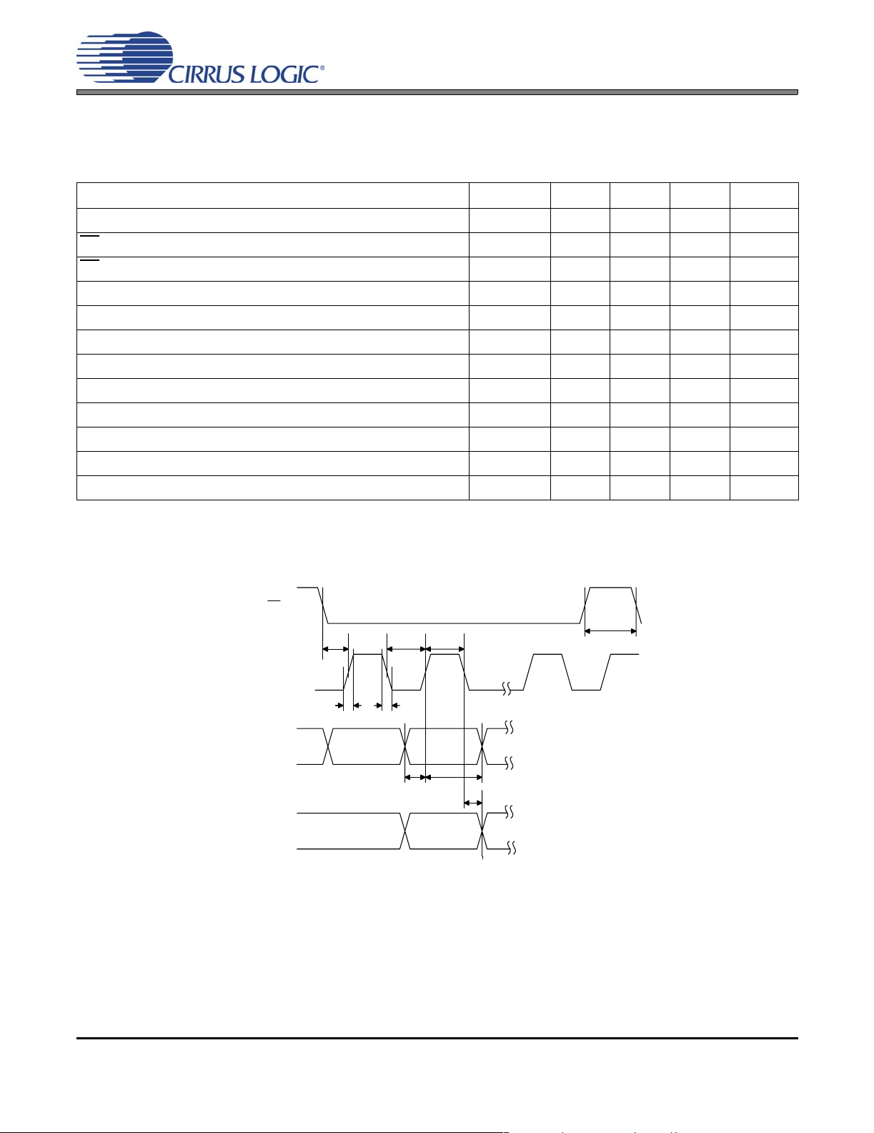
1. CHARACTERISTICS AND SPECIFICATIONS
(All Min/Max characteristics and specifications are guaranteed over the Specified Operating Conditions. Typical
performance characteristics and spe cif icat ion s ar e de riv e d from measurements taken at nominal supply voltages
and T
= 25°C.)
A
SPECIFIED OPERATING CONDITIONS
(GND = 0 V, all voltages with respect to ground)
Parameter Symbol Min Typ Max Units
DC Power Supply
Digital 2.5 V VD 2.37 2.5 2.63 V
XTAL (Note 1) 2.5 V
3.3 V
5.0 V
PWM Interface 3.3 V
5.0 V
Serial Audio Interface 2.5 V
3.3 V
5.0 V
Control Interface 2.5 V
3.3 V
5.0 V
Ambient Operating Temperature
Commercial -CQZ
Automotive -DQZ
VDX 2.37
3.14
4.75
VDP 3.14
4.75
VLS 2.37
3.14
4.75
VLC 2.37
3.14
4.75
T
A
-10
-40
2.5
3.3
5.0
3.3
5.0
2.5
3.3
5.0
2.5
3.3
5.0
-
-
2.63
3.47
5.25
3.47
5.25
2.63
3.47
5.25
2.63
3.47
5.25
+70
+85
V
V
V
V
V
V
V
V
V
V
V
°C
°C
Notes:
1. When using external crystal, VDX = 3.14 V(min). When using clock signal input, VDX = 2.37 V(min).
ABSOLUTE MAXIMUM RATINGS
(GND = 0 V; all voltages with respect to ground.)
Parameters Symbol Min Max Units
DC Power Supply Digital
XTAL
PWM Interface
Serial Audio Interface
Control Interface
Input Current (Note 2) I
Digital Input Voltage PWM Interface
(Note 3) Serial Audio Interface
Control Interface
Ambient Operating Temperature -CQ
(power applied) -DQ
Storag e Temperature T
WARNING:Operation at or beyond these limits may result in permanent damage to the device. Normal operation
is not guaranteed at these extremes.
2. Any pin except supplies. Transient currents of up to ±100 mA on the input pins will not cause SCR latch-up.
3. The maximum over/under voltage is limited by the input current.
VD
VDX
VDP
VLS
VLC
in
V
IND-PWM
V
IND-S
V
IND-C
T
stg
A
-0.3
-0.3
-0.3
-0.3
-0.3
-±10mA
-0.3
-0.3
-0.3
-20
-50
-65 +150 °C
3.5
6.0
6.0
6.0
6.0
VDP+0.4
VLS+0.4
VLC+0.4
+85
+95
V
V
V
V
V
V
V
V
°C
°C
8 DS633F1
Page 9
CS44600
DC ELECTRICAL CHARACTERISTICS
(GND = 0 V, all voltages with respect to ground; DAI_MCLK = 12.288 MHz, XTAL = 24.576 MHz, PWM Switch
Rate = 384 kHz unless otherwise specified.)
Parameter Symbol Min Typ Max Units
Normal Operation (Note 4)
Power Supply Current (Note 5) VD = 2.5 V
VDX = 3.3 V
VDP = 3.3 V
VLS = 3.3 V
VLC = 3.3 V (Note 6)
I
I
I
I
I
D
DX
DP
LS
LC
-
-
-
-
-
150
2
1.2
150
250
-
-
-
-
Power Dissipation VD=2.5 V, VDX = VDP = VLS = VLC = 3.3 V - 387 500 mW
Power Supply Rejection Ratio (Note 7) (1 kHz)
(60 Hz)
PSRR -
15
-
40
-
Power-Down Mode (Note 8)
Power Supply Current All Supplies except VDX (Note 9) I
pd
-80-µA
mA
mA
mA
µA
µA
dB
dB
4. Normal operation is defined as RST
= HI with a 997 Hz, 0 dBFS input.
5. Current consumption increas es with increasing XTAL clock rates and PWM switch rates. Variance between DAI clock rates is negligible.
6. I
measured with no external loading on the SDA pin.
LC
7. Valid with PSRR function enabled and the recommended external ADC (CS4461) and filtering.
8. Power down mode is defined as RST
9. When RST
pin = LOW, the internal oscillator is active to provide a valid clock for the SYS_CLK output.
pin = LOW with all clock and data lines held static.
DIGITAL INTERFACE CHARACTERISTICS
(GND = 0 V, all voltages with respect to ground)
Parameters (Note 10) Symbol Min Typ Max Units
High-Level Input Voltage XTAL
PWM Interface
Serial Audio Interface
Control Interface
Low-Level Input Voltage XTAL
PWM Interface
Serial Audio Interface
Control Interface
High-Level Output Voltage at I
= -2 mA PWM Interface
o
Serial Audio Interface
V
Control Interface
Low-Level Output Voltage at I
= 2 mA PWM Interface
o
Serial Audio Interface
Control Interface
Input Leakage Current I
0.7xVDX
V
IH
0.7xVDP
0.7xVLS
0.7xVLC
-
V
IL
-
-
-
VDP-1.0
OH
VLS-1.0
VLC-1.0
-
V
OL
-
-
in
--±10µA
-
-
-
-
-
-
-
-
-
-
-
-
-
-
Input Capacitance - - 8 pF
10. Serial Port signals include: SYS_CLK, DAI_MCLK, DAI_SCLK, DAI_LRCK, DAI_SDIN1-3
Control Port signals include: SCL/CCLK, SDA/CDOUT, AD0/CS
, AD1/CDIN, INT, RST, MUTE
PWM signals include: PWMOUTA1-B3, PSR_MCLK, PSR_SYNC, PSR_DATA, PS_SYNC, GPIO[6:0]
-
-
-
-
0.2xVDX
0.2xVDP
0.2xVLS
0.2xVLC
-
-
-
0.45
0.45
0.45
V
V
V
V
V
V
V
V
V
V
V
V
V
V
DS633F1 9
Page 10
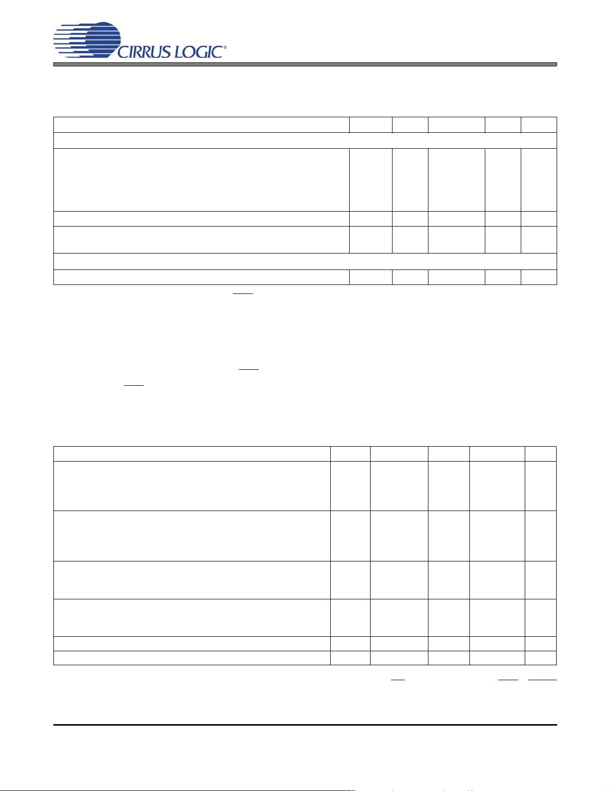
CS44600
PWM OUTPUT PERFORMANCE CHARACTERISTICS
(Logic “0” = GND = 0 V; Logic “1” = VLS = VLC; VD = 2.5 V; DAI_MCLK = 12.288 MHz; XTAL= 24.576 MHz; PWM
Switch Rate = 384 kHz; Fs = 32 kHz to 192 kHz; Measurement bandwidth is 10 Hz to 20 kHz unless otherwise
specified; Performance measurements taken with a full-scale 997 Hz.)
Parameter Symbol Min Typ Max Unit
Dynamic Performance (Note 11)
24-Bits A-Weighted
unweighted
16-Bits unweighted
Total Harmonic Distortion + Noise (Note 11)
24-Bits 0 dB
THD+N -
-20 dB
-60 dB
Idle Channel Noise / Signal-to-Noise Ratio - 110 - dB
Interchannel Isolation (1 kHz) - 100 - dB
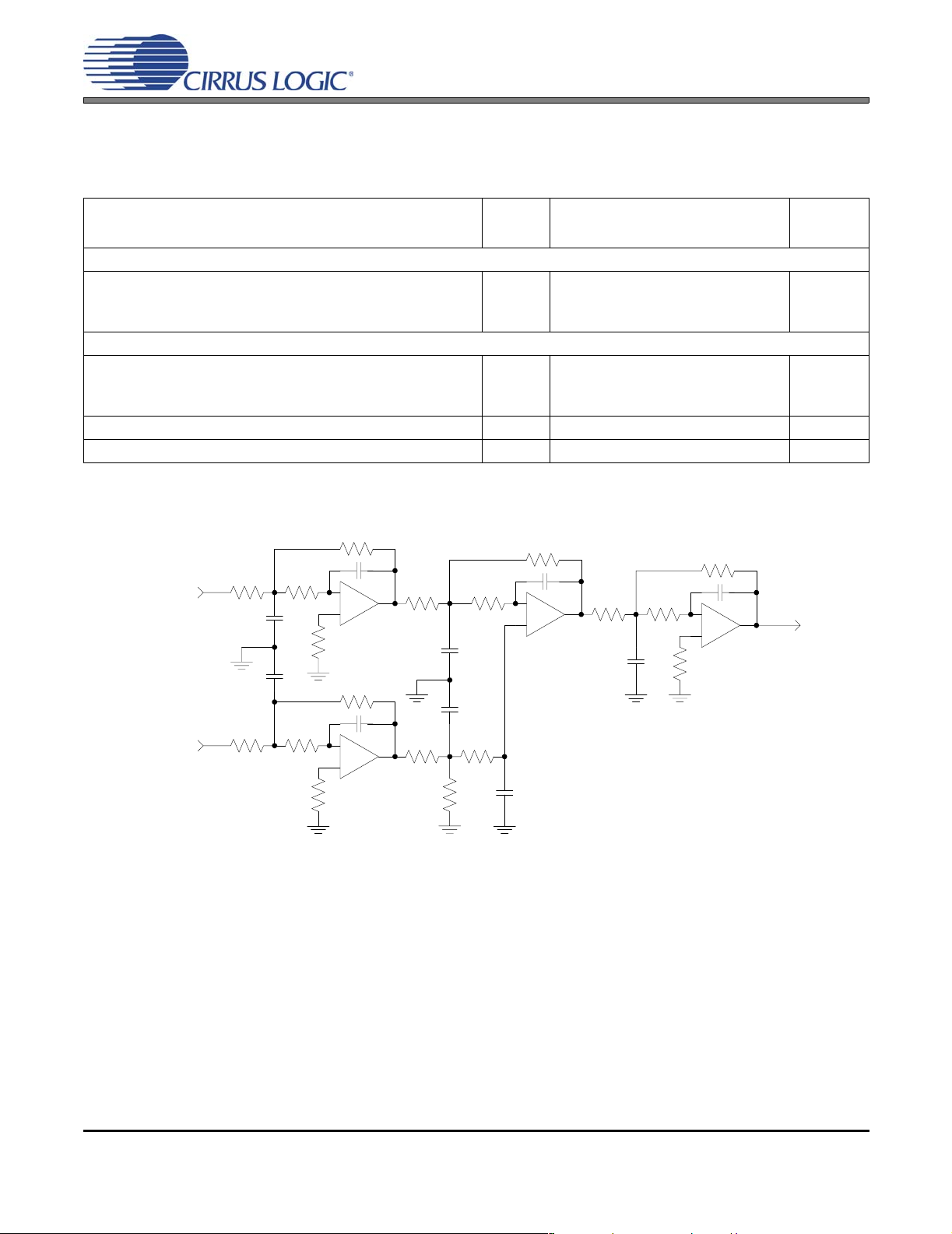
11. Performance characteristics measured using filter shown in Figure 1.
102
99
-
-
-
108
105
96
-90
-77
-45
-
-
-
-85
-
-
dB
dB
dB
dB
dB
dB
PWMOUTxx+
PWMOUTxx-
+
+
Figure 1. Performance Characteristics Evaluation Active Filter Circuit
+
+
Analog
Output
10 DS633F1
Page 11
CS44600
PWM FILTER CHARACTERISTICS
(Logic “0” = GND = 0 V; Logic “1” = VLS = VLC; VD = 2.5 V; DAI_MCLK = 12.288 MHz; XTAL = 24.576 MHz; PWM
Switch Rate = 384 kHz; Fs = 32 kHz to 192 kHz; Measurement bandwidth is 10 Hz to 20 kHz unless otherwise
specified.)
Parameter UnitMin Typ Max
Digital Filter Response (Note 12)
Passband
OSRATE = 0b to -0.01 dB corner
to -3 dB corner
OSRATE = 1b (Note 13) to -0.01 dB corner
to -3 dB corner
Frequency Response
OSRATE = 0b 10 Hz to 20 kHz
OSRATE = 1b (Note 13) 10 Hz to 40 kHz
Group Delay (Note 14) ms
De-emphasis Error Fs = 32 kHz
(Relative to 1 kHz) Fs = 44.1 kHz
Fs = 48 kHz
12. Filter response is not production tested but is characterized and guaranteed by design.
13. XTAL = 49.152 MHz; PWM Switch Rate = 768 kHz; Fs = 96 kHz to 192 kHz.
14. The equation for the group delay through the sample rate converter with OSRATE = 0b is (8.5 / Fsi) + (10
/ Fso) ± (4.5 / Fsi). The equation for the group delay through the sample rate converter with OSRATE = 1b
is (8.5 / Fsi) + (20 / Fso) ± (4.5 / Fsi).
0
0
0
0
-0.8
-1.2
-
-
-
-
-
-
-
-
-
-
-
-
1.6
24.0
3.3
44.5
+0.02
+0.02
±0.23
±0.14
±0.09
kHz
kHz
kHz
kHz
dB
dB
dB
dB
dB
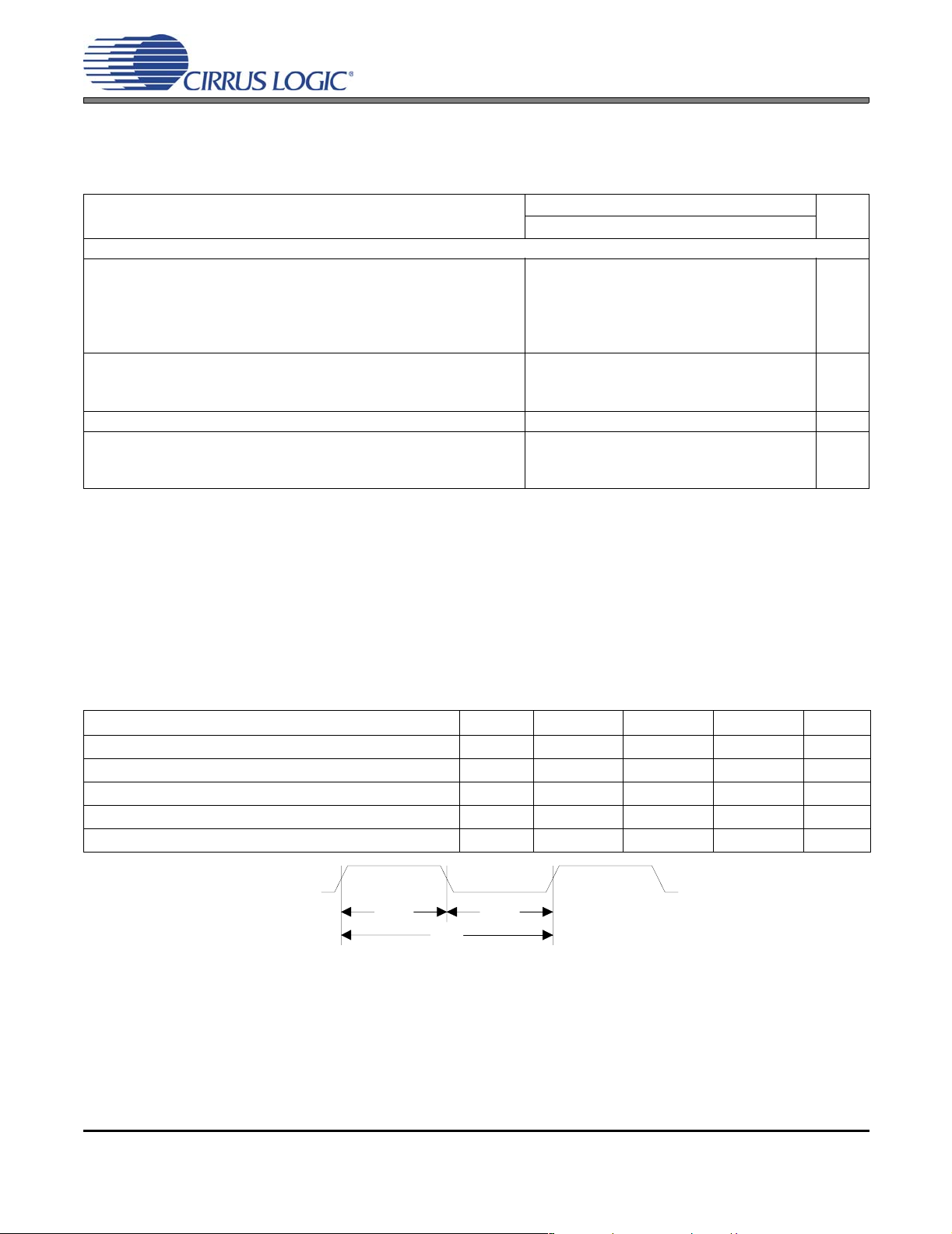
SWITCHING CHARACTERISTICS - XTI
(VD = 2.5 V, VDP = VLC = VLS = 3.3 V, VDX = 2.5 V to 5.0 V; Inputs: Logic 0 = GND, Logic 1 = VDX)
Parameter Symbol Min Typ Max Unit
XTI period t
XTI high time t
XTI low time t
XTI Duty Cycle 45 50 55 %
External Crystal operating frequency 24.576 --- 54 MHz
clki
clkih
clkil
XTI
t
clkih
t
Figure 2. XTI Timings
clki
t
clkil
18.518 --- 40.69 ns
8.34 --- 22.38 ns
8.34 --- 22.38 ns
DS633F1 11
Page 12
CS44600
SWITCHING CHARACTERISTICS - SYS_CLK
(VD = 2.5 V, VDP = VLC = VDX = 3.3 V, VLS = 2.5 V to 5.0 V, Cload = 50 pF)
Parameter Symbol Min Typ Max Unit
SYS_CLK Period t
SYS_CLK Duty Cycle 45 50 55 %
sclki
18.518 --- --- ns
SYS_CLK
t
sclki
Figure 3. SYS_CLK Timings
SWITCHING CHARACTERISTICS - PWMOUTA1-B3
(VD = 2.5 V, VLS = VLC = VDX = 3.3 V, VDP = 3.3 V to 5.0 V unless otherwise specified, Cload = 10 pF)
Parameter Symbol Min Typ Max Unit
PWMOUTxx Period t
Rise Time of PWMOUTxx VDP = 5.0 V
VDP = 3.3 V
Fall Time of PWMOUTxx VDP = 5.0 V
VDP = 3.3 V
pwm
t
r
t
f
2.60 - 1.18 µs
-
-
-
-
1.6
2.1
1.1
1.4
-
-
-
-
ns
ns
ns
ns
t
r
t
f
PWMOUTxx
t
pwm
Figure 4. PWMOUTxx Timings
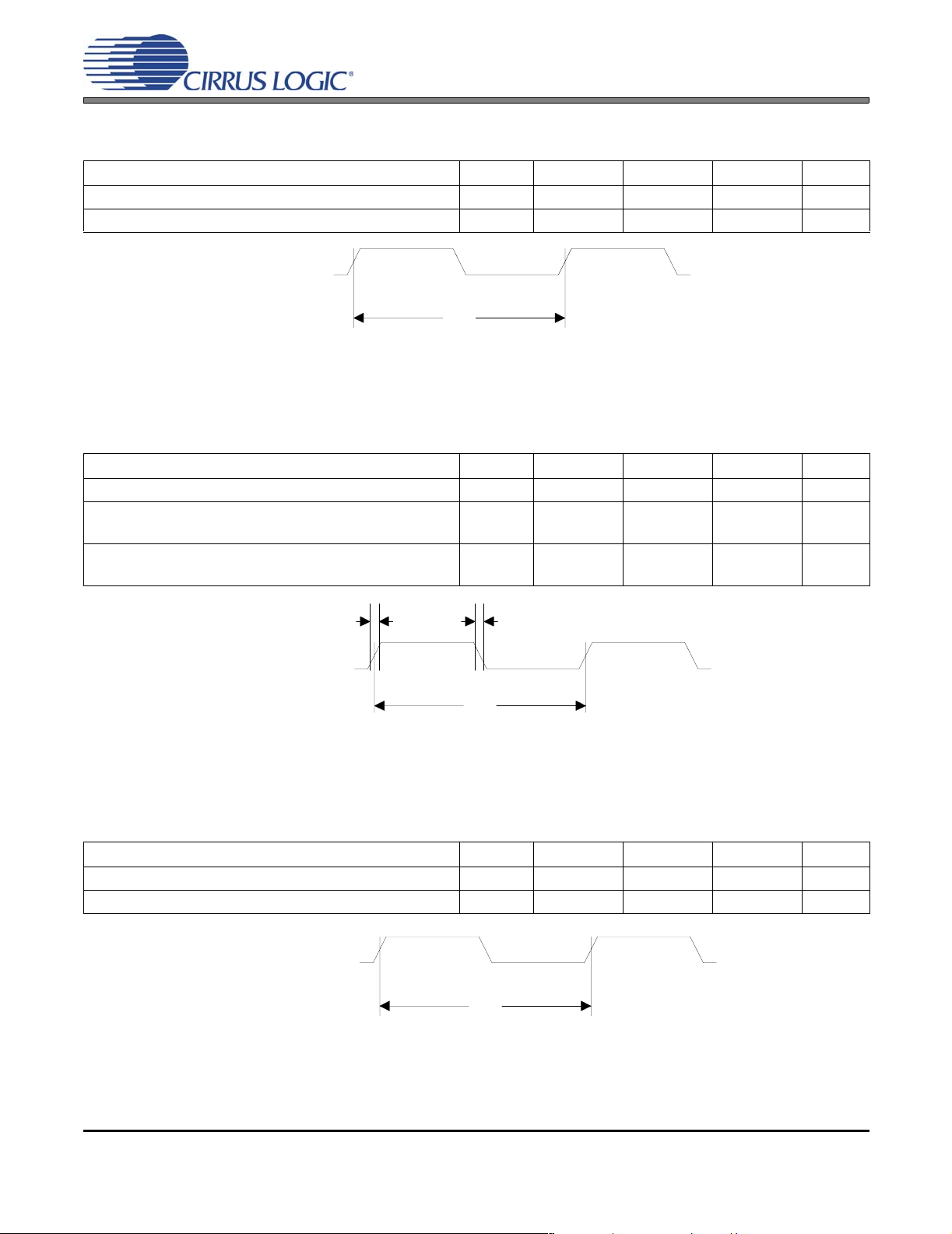
SWITCHING CHARACTERISTICS - PS_SYNC
(VD = 2.5 V, VLS = VLC = VDX = 3.3 V, VDP = 3.3 V to 5.0 V, Cload = 20 pF)
Parameter Symbol Min Typ Max Unit
PS_SYNC Period t
PS_SYNC Duty Cycle 45 50 55 %
psclki
PS_SYNC
t
psclki
Figure 5. PS_SYNC Timings
592.576 --- --- ns
12 DS633F1
Page 13
CS44600
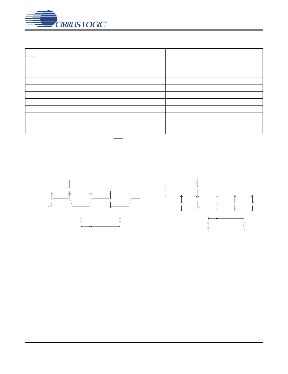
SWITCHING CHARACTERISTICS - DAI INTERFACE
(VD = 2.5 V, VDX = VDP = VLC = 3.3 V, VLS = 2.5 V to 5.0 V; Inputs: Logic 0 = GND, Logic 1 = VLS.)
Parameters Symbol Min Max Units
RST
pin Low Pulse Width (Note 15) 1-ms
DAI_MCLK Duty Cycle (Note 16) 40 60 %
DAI_SCLK Duty Cycle 45 55 %
DAI_LRCK Duty Cycle 45 55 %
DAI Sample Rate (Note 17) F
DAI_SDIN Setup Time Before DAI_SCLK Rising Edge t
DAI_SDIN Hold Time After DAI_SCLK Rising Edge t
DAI_SCLK High Time t
sckh
DAI_SCLK Low Time t
DAI_LRCK Setup Time Before DAI_SCLK Rising Edge t
DAI_SCLK Rising Edge Before DAI_LRCK Edge t
lrckd
s
ds
dh
sckl
lrcks
32 192 kHz
10 - ns
10 - ns
20 - ns
20 - ns
25 - ns
25 - ns
15. After powering up, the CS44600, RST
should be held low until after the power supplies and clocks are set-
tled.
16. See Table 1 on page 26 for suggested MCLK frequencies.
17. Max DAI sample rate is 96 kHz for One Line and TDM modes of operation.
DAI_LRCK
DAI_SCLK
DAI_SDINx
t
lrckd
t
lrcks
t
sckh
t
ds
t
dh
t
sckl
Figure 6. Serial Audio Interface Timing Figure 7. Serial Audio Interface Timing - TDM Mode
DAI_LRCK
(input)
DAI_SCLK
(input)
DAI_SDIN1
t
lrcks
t
lrckd
t
lrcks
t
sckh
t
ds
t
dh
MSB MSB-1
t
sckl
DS633F1 13
Page 14
CS44600
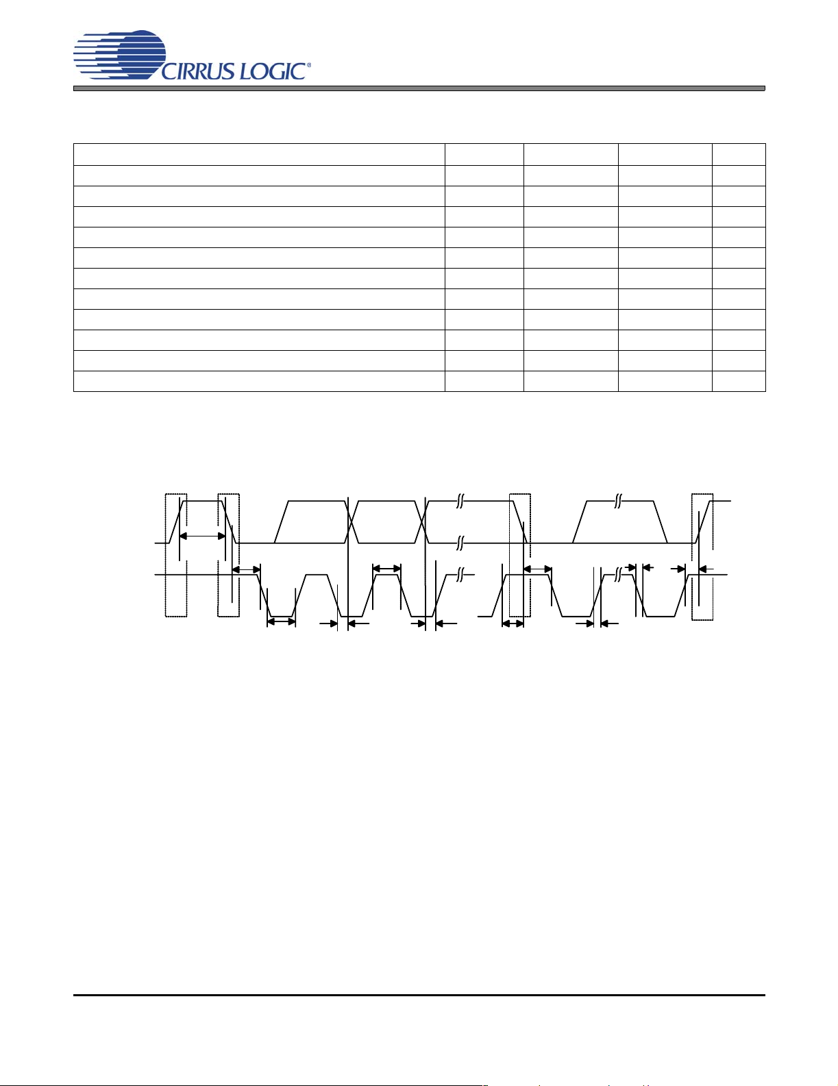
SWITCHING CHARACTERISTICS - CONTROL PORT - I²C FORMAT
(VD = 2.5 V, VDX = VDP = VLS = 3.3 V; VLC = 2.5 V to 5.0 V; Inputs: Logic 0 = GND, Logic 1 = VLC, CL=30pF)
Parameter Symbol Min Max Unit
SCL Clock Frequency f
Bus Free Time between Transmissions t
Start Condition Hold Time (prior to first clock pulse) t
Clock Low time t
Clock High Time t
Setup Time for Repeated Start Condition t
SDA Hold Time from SCL Falling (Note 18) t
SDA Setup time to SCL Rising t
Rise Time of SCL and SDA t
Fall Time SCL and SDA t
Setup Time for Stop Condition t
susp
scl
buf
hdst
low
high
sust
hdd
sud
r
f
- 100 kHz
4.7 - µs
4.0 - µs
4.7 - µs
4.0 - µs
4.7 - µs
10 - ns
250 - ns
-1000ns
-300ns
4.7 - µs
18. Data must be held for sufficient time to bridge the transition time, t
Repeated
Stop Start
Start
SDA
t
buf
t
hdst
t
high
SCL
t
low
t
hdd
Figure 8. Control Port Timing - I²C Format
t
sud
t
sust
, of SCL.
f
t
hdst
Stop
t
f
t
r
t
susp
14 DS633F1
Page 15
CS44600
SWITCHING CHARACTERISTICS - CONTROL PORT - SPI FORMAT
(VD = 2.5 V, VDP = VLS = 3.3 V; VLC = 2.5 V to 5.0 V; Inputs: Logic 0 = GND, Logic 1 = VLC, CL=30pF)
Parameter Symbol Min Typ Max Units
CCLK Clock Frequency f
CS
High Time between Transmissions t
CS
Falling to CCLK Edge t
CCLK Low Time t
CCLK High Time t
CDIN to CCLK Rising Setup Time t
CCLK Rising to DATA Hold Time (Note 19) t
CCLK Falling to CDOUT Stable t
Rise Time of CDOUT t
Fall Time of CDOUT t
Rise Time of CCLK and CDIN (Note 20) t
Fall Time of CCLK and CDIN (Note 20) t
sck
csh
css
scl
sch
dsu
dh
pd
r1
f1
r2
f2
19. Data must be held for sufficient time to bridge the transition time of CCLK.
20. For f
<1 MHz.
sck
CS
0-6.0MHz
1.0 - - µs
20 - - ns
66 - - ns
66 - - ns
40 - - ns
15 - - ns
- - 50 ns
- - 25 ns
- - 25 ns
- - 100 ns
- - 100 ns
CCLK
CDIN
CDOUT
t
t
sch
t
dsu
scl
t
f2
t
dh
t
pd
t
css
t
r2
Figure 9. Control Port Timing - SPI Format
t
csh
DS633F1 15
Page 16
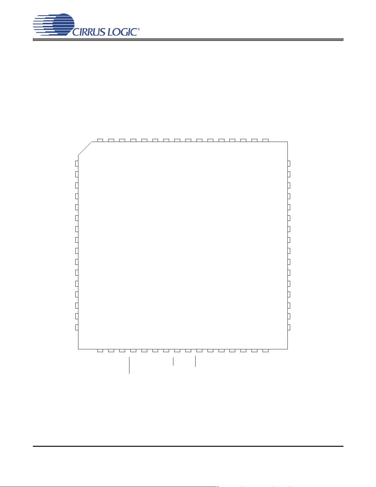
2. PIN DESCRIPTIONS
CS44600
GND
PSR_EN
PS_SYNC
GND
XTI
XTO
VDX
SYS_CLK
DAI_MCLK
DAI_SCLK
DAI_LRCK
DAI_SDIN1
DAI_SDIN2
DAI_SDIN3
PWMOUTA1+
64 63 62 61 60 59 58 57 56 55 54 53 52 51 50 49
1
2
3
4
5
6
7
8
9
10
11
12
13
14
VDP
PWMOUTA1-
PWMOUTB1+
PWMOUTB1-
GND
PWMOUTA2+
CS44600
VDP
PWMOUTA2-
PWMOUTB2+
GND
PWMOUTB2-
PSR_SYNC
PSR_RESET
PSR_DATAL
PSR_MCLK
GND
48
PWMOUTA3+
47
PWMOUTA3-
46
VDP
45
PWMOUTB3+
44
PWMOUTB3-
43
GND
42
NC
41
NC
40
VDP
39
NC
38
NC
37
GND
36
GPIO0
35
NC
VLS
15
16
17 18 19 20 21 22 23 24 25 26 27 28 29 30 31 32
VLC
VD
GND
MUTE
SCL/CCLK
Figure 10. CS44600 Pinout Diagram
AD1/CDIN
SDA/CDOUT
INT
AD0/CS
RST
VD
GND
GPIO3
GPIO6
GPIO4
GPIO5
34
33
GPIO1
GPIO2
16 DS633F1
Page 17

Pin Name Pin # Pin Description
PS_SYNC 3
XTI 5
XTO 6 Crystal Oscillator Output (Output) - Crystal Oscillator output.
SYS_CLK 8
DAI_MCLK 9 Digital Audio Input Master Clock (Input) - Master audio clock.
Power Supply Synchronization Clock (Output) - The PWM synchronized clock to the
switch mode power supply.
Crystal Oscillator Input (Input) - Crystal Oscillator input or accepts an external clock
input signal that is used to drive the internal PWM core logic.
External System Clock (Output) - Clock output. This pin provides a divided down clock
derived from the XTI input.
CS44600
DAI_SCLK 10
DAI_LRCK 11
DAI_SDIN1
DAI_SDIN2
DAI_SDIN3
MUTE 20
SCL/CCLK 21
SDA/CDOUT 22
AD1/CDIN 23
AD0/CS
INT 25
RST 26
GPIO6 29
12
1314Digital Audio Input Serial Data (Input) - Input for two’s complement serial audio data.
24
Digital Audio Input Serial Clock (Input) - Serial clock for the Digital Audio Input Inter-
face. The clock frequency is a multiple of the Left/Right Clock running at Fs.
Digital Audio Input Left/Right Clock (Input) - Determines which channel, Left or Right,
is currently active on the serial audio data line. The rate is determined by the sampling frequency Fs.
Mute (Input) - The device will perform a hard mute on all channels. All internal registers
are not reset to their default settings.
Serial Control Port Clock (Input) - Serial clock for the serial control port. Requires an
external pull-up resistor to the logic interface voltage in I²C mode as shown in the Typical
Connection Diagram.
Serial Control Data (Input/Output) - SDA is a data I/O line in I²C mode and requires an
external pull-up resistor to the logic interface voltage, as shown in the Typical Connection
Diagram.; CDOUT is the output data line for the control port interface in SPI mode.
Address Bit 1 (I²C)/Serial Control Data (SPI) (Input) - AD1 is a chip address pin in I²C
mode.;CDIN is the input data line for the control port interface in SPI mode.
Address Bit 0 (I²C)/Control Port Chip Select (SPI) (Input) - AD0 is a chip address pin in
I²C mode; CS
Interrupt Request (Output) - CMOS or open-drain interrupt request output. This pin is
driven to the configured active state to indicate that the PWM Controller has status data
that should be read by the host.
Reset (Input) - The device enters a low power mode and all internal registers are reset to
their default settings when low.
General Purpose Input, Output (Input/Output) - This pin is configured as an input follow-
ing a RST
be individually controlled by the Host Controller.
is the chip select signal in SPI mode.
condition. It can be configured as a general purpose input or output which can
General Purpose Input, Output (Input/Output) - This pin is configured as an input follow-
GPIO5 30
GPIO4 31
DS633F1 17
ing a RST
be individually controlled by the Host Controller.
General Purpose Input, Output (Input/Output) - This pin is configured as an input follow-
ing a RST
be individually controlled by the Host Controller.
condition. It can be configured as a general purpose input or output which can
condition. It can be configured as a general purpose input or output which can
Page 18
GPIO3 32
GPIO2 33
GPIO1 34
GPIO0 35
PSR_MCLK 49
PSR_DATAL 50
CS44600
General Purpose Input, Output (Input/Output) - This pin is configured as an input follow-
ing a RST condition. It can be configured as a general purpose input or output which can
be individually controlled by the Host Controller.
General Purpose Input, Output (Input/Output) - This pin is configured as an input follow-
ing a RST
be individually controlled by the Host Controller.
General Purpose Input, Output (Input/Output) - This pin is configured as an input follow-
ing a RST
be individually controlled by the Host Controller.
General Purpose Input, Output (Input/Output) - This pin is configured as an input follow-
ing a RST
be individually controlled by the Host Controller.
Power Supply Rejection Master Clock (Output) - Master audio clock for externa l PSR
ADC (CS4461).
Power Supply Rejection Input Serial Data (Input) - Input for serial audio data from
external PSR ADC (CS4461).
condition. It can be configured as a general purpose input or output which can
condition. It can be configured as a general purpose input or output which can
condition. It can be configured as a general purpose input or output which can
PSR_SYNC 51
PSR_RESET 52
PSR_EN 2
PWMOUTA1+
PWMOUTA1PWMOUTB1+
PWMOUTB1PWMOUTA2+
PWMOUTA2PWMOUTB2+
PWMOUTB2PWMOUTA3+
PWMOUTA3PWMOUTB3+
PWMOUTB3-
VDX 7 Crystal Power (Input) - Positive power supply for the Crystal section.
VD 19, 27 Digital Power (Input) - Positive power supply for the digital section.
VLC 17
VLS 16
Power Supply Rejection Sync Clock (Input) - Synchronization signal for external PSR
ADC (CS4461).
Power Supply Rejection Reset (Output) - The reset pin for the external Power Supply
Rejection circuitry.
Power Supply Rejection Enable (Output) - The enable pin for the external Power Supply
Rejection circuitry.
64
63
61
60
58
57
PWM Output (Output) - PWM control signals for the Class D amplifier backend.
55
54
47
46
44
43
Host Interface Power (Input) - Determines the required signal level for the digital
input/output signals for the host interface.
Digital Audio Interface Power (Input) - Dete rmines the required signal level fo r the digital
input signals for the digital audio interface.
VDP
GND
18 DS633F1
39, 45,
56, 62
1, 4,
18, 28,
36, 42,
48, 53,
PWM Interface Power (Input) - Determines the required signal level for the digital
input/output signals for the PWM and GPIO interface.
Digital Ground (Input) - Ground reference for digital circuits.
59
Page 19
CS44600
2.1 I/O Pin Characteristics
Power
Signal Name
RST VLC Input - 2.5 V and 3.3/5.0 V TTL Compatible.
SCL/CCLK VLC Input - 2.5 V and 3.3/5.0 V TTL Compatible, with Hysteresis.
Rail I/O Driver Receiver
SDA/CDOUT VLC
AD0/CS
AD1/CDIN VLC Input - 2.5 V and 3.3/5.0 V TTL Compatible, Internal pull-up.
INT VLC Output
MUTE VLC Input - 2.5 V and 3.3/5.0 V TTL Compatible.
DAI_SDINx VLS Input - 2.5 V and 3.3/5.0 V TTL Compatible.
DAI_SCLK VLS Input - 2.5 V and 3.3/5.0 V TTL Compatible.
DAI_LRCK VLS Input - 2.5 V and 3.3/5.0 V TTL Compatible.
DAI_MCLK VLS Input - 2.5 V and 3.3/5.0 V TTL Compatible.
SYS_CLK VLS Output 2.5-5.0 V, CMOS XTI VDX Input - 2.5 V and 3.3/5.0 V TTL Compatible, Internal pull-down.
XTO VDX Output - -
GPIOx VDP
PWMOUTAx+/- VDP Outp ut 3.3/5.0 V, CMOS -
PWMOUTBx+/- VDP Output 3.3/5.0 V, CMOS -
VLC Input - 2.5 V and 3.3/5.0 V TTL Compatible, Internal pull-up.
Input /
Output
Input /
Output
2.5-5.0 V,
CMOS/Open Drain
2.5-5.0 V,
CMOS/Open Drain
3.3/5.0 V,
CMOS/Open Drain
2.5 V and 3.3/5.0 V TTL Compatible, with Hysteresis.
-
3.3/5.0 V TTL Compatible.
PSR_MCLK VDP Output 3.3/5.0 V, CMOS PSR_SYNC VDP Input - 3.3/5.0 V TTL Compatible, Internal pull-up.
PSR_DATA VDP Input - 3.3/5.0 V TTL Compatible, Internal pull-up.
PSR_EN VDP Output 3.3/5.0 V, CMOS PSR_RESET VDP Output 3.3/5.0 V, CMOS PS_SYNC VDP Output 3.3/5.0 V, CMOS -
DS633F1 19
Page 20
3. TYPICAL CONNECTION DIAGRAMS
CS44600
+2.5 V
+3.3 V to
+5.0 V
+2.5 V to
+5.0 V
10 µF
+
0.1 µF
0.1 µF
0.1 µF
24.576 MHz
to 54 MHz
0.1 µF
Digital
Audio
Processor
0.01 µF
0.01 µF
0.01 µF
XTAL
0.01 µF
0.1 µF
0.01 µF
VD
VD
CS44600
VDX
XTI
XTO
VLS
SYS_CLK
DAI_MCLK
DAI_SCLK
DAI_LRCK
DAI_SDIN1
DAI_SDIN2
DAI_SDIN3
0.1 µF
0.01 µF
VDP
0.1 µF
0.01 µF
0.01 µF
PWMOUTA1+
PWMOUTA1-
GPIO1
PWMOUTB1+
PWMOUTB1-
GPIO2
PWMOUTA2+
PWMOUTA2-
GPIO3
PWMOUTB2+
PWMOUTB2-
GPIO4
PWMOUTA3+
PWMOUTA3-
GPIO5
PWMOUTB3+
PWMOUTB3-
GPIO6
GPIO0
0.1 µF
10 µF
+3.3 V to +5.0 V
PWM IN1
CONTROL
PWM IN2
CONTROL
PWM IN3
CONTROL
PWM IN4
CONTROL
PWM IN5
CONTROL
PWM IN6
CONTROL
OUT1
STATUS
OUT2
STATUS
OUT3
STATUS
OUT4
STATUS
OUT5
STATUS
OUT6
STATUS
Front Left
Front Right
Surr. Left
Surr. Right
Center
Subwoofer
MUTE
INT
Ω
2 k
RST
SCL/CCLK
SDA/CDOUT
AD1/CDIN
AD0/CS
VLC
GND
PS_SYNC
PSR_MCLK
PSR_SYNC
PSR_DATA
PSR_EN
PSR_RESET
Power Supply Sync Clock
Power Supply Rail
CS4461
ADC
Optional
Micro-
Controller
Ω
+2.5 V
to +5.0 V
Note: Resistors are required for
I²C control port operation
2 k
See
Note
0.1 µF
Figure 11. Typical Full-Bridge Connection Diagram
20 DS633F1
Page 21
CS44600
+2.5 V
+3.3 V to
+5.0 V
+2.5 V to
+5.0 V
10 µF
+
0.1 µF
0.1 µF
0.1 µF
24.576 MHz
to 54 MHz
0.1 µF
Digital
Audio
Processor
0.01 µF
0.01 µF
0.01 µF
XTAL
0.01 µF
0.1 µF
0.01 µF
VD
VD
CS44600
VDX
XTI
XTO
VLS
SYS_CLK
DAI_MCLK
DAI_SCLK
DAI_LRCK
DAI_SDIN1
DAI_SDIN2
DAI_SDIN3
0.1 µF
0.01 µF
VDP
0.1 µF
0.01 µF
0.01 µF
PWMOUTA1+
PWMOUTA1PWMOUTB1+
PWMOUTB1-
GPIO3
GPIO0
PWMOUTA2+
PWMOUTA2-
PWMOUTB2+
PWMOUTB2-
GPIO4
GPIO1
PWMOUTA3+
PWMOUTA3-
PWMOUTB3+
PWMOUTB3-
GPIO5
GPIO2
0.1 µF
10 µF
+3.3 V to +5.0 V
PWM IN1
PWM IN2
CONTROL
PWM IN1
PWM IN2
CONTROL
PWM IN1
PWM IN2
CONTROL
OUT1
Front Left
OUT2
Front Right
STATUS
OUT1
Surr. Left
OUT2
Surr. Right
STATUS
OUT1
Center
OUT2
Subwoofer
STATUS
MUTE
INT
Ω
2 k
RST
SCL/CCLK
SDA/CDOUT
AD1/CDIN
AD0/CS
VLC
GND
PS_SYNC
PSR_MCLK
PSR_SYNC
PSR_DATA
PSR_EN
PSR_RESET
Power Supply Sync Clock
Power Supply Rail
CS4461
ADC
Optional
Micro-
Controller
Ω
+2.5 V
to +5.0 V
Note: Resistors are required for
I²C control port operation
2 k
See
Note
0.1 µF
Figure 12. Typical Half-Bridge Connection Diagram
DS633F1 21
Page 22

4. APPLICATIONS
4.1 Overview
The CS44600 is a multi-channel digital-to-PWM Class D audio system controller including interpolation,
sample rate conversion, half- and full-bridge PWM driver outputs, and power supply rejection feedb ack in a
64-pin LQFP package. The architecture uses a di rect-t o-digital ap proach that maintains digita l signal integrity to the final output filter, minimizing analog interference effects which negatively affect system performance.
The CS44600 integrates on-chip sample rate conversion, digital volume control, peak detect with volume
limiter, de-emphasis, programmab le interrup t condit ions, and th e abilit y to chan ge the PW M switch ra te to
eliminate AM frequency interference. The CS44600 also has a programmable load compensation filter,
which allows the speaker load to vary while the output filter remains fixed, maintaining a flat frequency response. For single-ended half-bridge applications PWM Popguard
and realtime power supply feedback reduces noise coupling from the power supp ly. The PWM amplifier can
achieve greater than 90% efficiency. This efficiency provides for a smaller device package, less heat sink
requirements, and smaller power supplies.
The CS44600 is ideal for audio systems requiring wide dynamic range, negligible distortion, and low noise
such as A/V receivers, DVD receivers, digital speaker, and automotive audio systems.
4.2 Feature Set Summary
CS44600
®
reduces the transient pops an d clicks
Core Features
• 2.5 V digital core voltage, VD.
• VLC voltage pin for host interface logic levels between 2.5 V and 5.0 V.
• VLS voltage pin for digital audio interface logic levels between 2.5 V and 5.0 V.
• VDP voltage pin for PWM backend interface logic levels between 3.3 V and 5.0 V.
• VDX voltage pin for clock input signals between 2.5 V and 5.0 V.
Clocking
• Minimum of 128Fs DAI_MCLK for DAI serial interface.
• DAI interface uses automatic detection of LRCK/MCLK ratio to configure internal DAI/SRC clocks.
• All PWM Processing clocks generated internally via:
– An external crystal - 24.576 MHz to 54 MHz, or
– XTI input pin capable of supporting a clock signal at the VDX voltage level.
• Programmable divide of XTI by 1, 2, 4, 8 for SYS_CLK output.
• Programmable divide of XTI by 32, 64, 128, 256 for PS_SYNC (power supply synchronization signal).
Digital Audio Playback
• Supports 32 kHz, 44.1 kHz, 48 kHz, 88.2 kHz, 96 kHz, 176.4 kHz and 192 kHz sample frequencies.
• High performance sample rate converter.
• 16, 20 and 24 bit audio sample lengths.
• De-emphasis for 32 kHz, 44.1 kHz, 48 kHz.
22 DS633F1
Page 23
• Digital volume control with soft ramp.
• Individual channel volume gain, attenuation and mute capability; +24 to -127 dB in 0.25 dB steps.
• Master volume attenuation; +24 to -127 dB in 0.25 dB steps.
• Peak Detect and Volume Limiter with programmable attack and release rates.
• Signal-clipping interrupt indicator.
Additional Features
• Contains a two-stage digital output filter for speaker impedance compensation.
• Provide s 7 prog ram mabl e GPIO pins with interr upt ge neratio n for easily int erfa cing to a va riety of com-
monly available power state parts. Interrupts can be masked.
• Selectable over-sample rate for increased audio bandwidth.
• Power supply clock output, PS_SYNC, with programmable divider
CS44600
FsIn FsOut
1,2,4,8
De-
Emphasis
128Fs
DAI_MCLK
DAI_LRCK
DAI_SCLK
DAI_SDINx
XTO
XTI
SYS_CLK
1, 1.5, 2,
3, 4, 6, 8
Ratio Detect
Digital Audio
Input Port
XTAL /
CLKIN
Figure 13. CS44600 Data Flow Diagram (Single Channel Shown)
4.3 Clock Generation
The sources for internal clock generation for the PWM processing are as follows:
• FsIn Domain:
– DAI_MCLK, minimum 128Fs
• FsOut Domain:
– XTI/XTO (Fundamental or 3
– Clock signal on XTI (VDX is used to set logic voltage level)
SRC
SRC_MCLK (128Fs)
Master
Volume
Channel
Volume
2-pole Load
Compensation
Filter
2.25
Clock Control
Σ
VOL
MOD_MCLK
PWM_MCLK
1,1.5,
2,4
AM Freq. Hop
(AM_FREQ_HOP)
rd
overtone crystal), or
mute
Over Sample
(OSRATE)
LIMITER
PEAK
DETECT
Over Sample
(OSRATE)
x2
Multibit
Σ∆
Modulator
PSR
Feedback
PWM Engine
Delay
Delay
PWM_OUT+
PWM_OUT-
DS633F1 23
Page 24

4.3.1 FsIn Domain Clocking
Common DAI_MCLK frequencies and sample rates are shown in Table 1.
Mode
(sample-rate range)
DAI_MCLK/LRCK Ratio −> 256x 384x 512x 768x 1024x
Single Speed
(4 to 50 kHz)
DAI_MCLK/LRCK Ratio −> 128x 192x 256x 384x 512x
Double Speed
(50 to 100 kHz)
DAI_MCLK/LRCK Ratio −> 64x 96x 128x 192x 256x
Quad Speed
(100 to 200 kHz)
Sample
Rate
(kHz)
32 8.1920 12.2880 16.3840 24.5760 32.7680
44.1 11.2896 16.9344 22.5792 33.8688 45.1584
48 12.2880 18.4320 24.5760 36.8640 49.1520
64 8.1920 12.2880 16.3840 24.5760 32.7680
88.2 11.2896 16.9344 22.5792 33.8688 45.1584
96 12.2880 18.4320 24.5760 36.8640 49.1520
176.4 n/a n/a 22.5792 33.8688 45.1584
192 n/a n/a 24.5760 36.8640 49.1520
Table 1. Common DAI_MCLK Frequencies
DAI_MCLK (MHz)
4.3.2 FsOut Domain Clocking
CS44600
To ensure the highest quality conversion of PWM signals, the CS44600 is capable of operating from a
fundamental mode or 3
to 54 MHz. If XTI is being directly driven by a clock signal, XTO can be left floating or tied to ground
through a pull-down resistor and the internal oscillator should be powered down using the PDN_XTAL bit
in register 02h.
rd
overtone crystal, or a clock signal attached to XTI, at a frequency of 24.576 MHz
XTI
Y1
C1
XTO
C2
Figure 14. Fundamental Mode Crystal Configuration
24 DS633F1
Page 25

CS44600
Y1
XTI
C1
XTO
L1
C3
Figure 15. 3rd Overtone Crystal Configuration
Appropriate clock dividers for each functional block and a programmable divider to support an output for
switched-mode power supply synchronization are provided. The clock generation for the CS44600 is
shown in the Figure 16.
XTO
XTI
System Clock
Divider
PWM Master
Clock Divider
C2
PWM_MCLK
PWM Modulator
Clock Divider
MOD_MCLKSYS_CLK
PS_SYNC
Power Supply
Sync. Divider
Figure 16. CS44600 Internal Clock Generation
Sample Rate Converter
Clock Divider
SRC_MCLK
DS633F1 25
Page 26
4.4 FsIn Clock Domain Modules
4.4.1 Digital Audio Input Port
The CS44600 interfaces to an external Digita l Audio Processor via the Digital Audio Input serial port, the
DAI serial port. The DAI port has 3 stereo data inputs with support for I²S, left-justified and right-justified
formats. The DAI port operates in slave operation only, where DAI_LRCK, DAI_SCLK and DAI_MCLK are
always inputs. The signal DAI_LR CK must be equal to the sample rate, Fs and must be synchronously
derived from the supplied master c lock, DAI_MCLK. The serial bit clock, DAI_SCLK, is used to sample
the data bits and must be synchronously derived from the master clock.
DAI_SDIN1, DAI_SDIN2, and DAI_SDIN3 are the serial data input pins supplying the associated internal
PWM channel modulators. The serial data interface format selection (left-justified, right-justified, I²S, one
line mode, or TDM) for the DAI serial port data input pins is configured using the appropriate bits in the
register “Misc. Configuration (address 04h)” on pag e 52. The serial audio data is presented in 2's complement binary form with the MSB first in all formats.
When operated in One Line Data Mode, 6 channels of PWM data are input on DAI_SDIN1. In TDM mode,
all 6 channels are multiplexed onto the DAI_SDIN1 data line. Table 2 outlines the serial port channel allocations.
Serial Data Input s Data mode Channel Assignments
DAI_SDIN1 Normal (I²S,LJ,RJ)
One Line #1 or #2
TDM
DAI_SDIN2 Normal (I²S,LJ,RJ)
One Line #1 or #2
TDM
DAI_SDIN3 Normal (I²S,LJ,RJ)
One Line #1 or #2
TDM
Table 2. DAI Serial Audio Port Channel Allocations
The DAI digital audio serial ports support 6 formats with varying bit depths from 16 to 24 as shown in Fig-
ure 17, Figure 18, Figure 19, Figure 20, Figure 21 and Figure 22. These formats are selected using the
configuration bits in the “Misc. Configuration (address 04h)” on page 52.
PWMOUTA1(left channel)/PWMOUTB1(right channel)
PWMOUTA1/A2/A3/B1/B2/B3
PWMOUTA1/A2/A3/B1/B2/B3
PWMOUTA2(left channel)/PWMOUTB2(right channel)
not used
not used
PWMOUTA3(left channel)/PWMOUTB3(right channel)
not used
not used
CS44600
26 DS633F1
Page 27
CS44600
4.4.1.1 I²S Data Format
For I²S, data is received most si gnificant bit first, one DAI_SCLK delay after the transition of DAI_LRCK,
and is valid on the rising edge of DAI_SCLK. For the I²S format, the left channel data is presente d when
DAI_LRCK is low; the right channel data is presented when DAI_LRCK is high.
DAI_LRCK
DAI_SCLK
DAI_ S DINx
MSB
-2 -3 -4 -5
-1
Left Channel
+3 +2 +1+5 +4
I²S Mode, Data Valid on Rising Edge of DAI_SCLK
Bits/Sample SCLK Rates
16 32, 48, 64, 128, 256 Fs
18 to 24 48, 64, 128, 256 Fs
4.4.1.2 Left-Justified Data Format
For left-justified format, data is received most significant bit first on the first DAI_SCLK after a DAI_LRCK
transition and is valid on the rising edge of DAI_SCLK. For the left-justified format, the left channel data
is presented when DAI_LRCK is high and the right channel data is presented when DAI_LRCK is low.
DAI_LRCK
DAI_SCLK
Left Channel
Right C hannel
LSB LSB
MSB
-1
-2 -3 -4
Figure 17. I²S Serial Audio Formats
Right Channel
+3 +2 +1+5 +4
DAI_S D INx
MSB LSB MSB LSB
-1 -2 -3 -4 -5
+3 +2 +1+5 +4
-1
-2 -3 -4
+3 +2 +1+5 +4
Left-Justified Mode, Data Valid on Rising Edge of DAI_SCLK
Bits/Sample SCLK Rate(s)
16 32, 48, 64, 128, 256 Fs
18 to 24 48, 64, 128, 256 Fs
Figure 18. Left-Justified Serial Audio Formats
DS633F1 27
Page 28

CS44600
4.4.1.3 Right-Justified Data Format
In the right-justified format, data is received most significant bit first and with the least significant bit presented on the last DAI_SCLK before the DAI_LRCK transition and is valid on the rising edge of
DAI_SCLK. For the right-justified format, the left channel data is presented when DAI_LRCK is high and
the right channel data is presented when DAI_LRCK is low. Either 16 bits per sample or 24 bits per sample are supported.
DAI_LRCK
DAI_SCLK
DAI_ S DINx
Left Channel
15 14 13 12 11 10
6543210987
15 14 13 12 11 10
Right Channel
6543210987
Right-Justified Mode, Data Valid on Rising Edge of DAI_SCLK
Bits/Sample SCLK Rate(s)
16 32, 48, 64, 128, 256 Fs
24 48, 64, 128, 256 Fs
Figure 19. Right-Justified Serial Audio Formats
4.4.1.4 One Line Mode #1
In One Line mode #1 format, data is received most significant bit first on the first DAI_SCLK after a
DAI_LRCK transition and is valid on the rising edge of DAI_SCLK. DAI_SCL K must oper ate at a 128F s
rate. DAI_LRCK identifies the start of a new frame and is eq ual to th e sa mple p eri od. DAI_L RCK is sa mpled as valid on the same clock edge as the most significant bit of the first data sample an d must be h eld
high for 64 DAI_SCLK periods. Each time slot is 20 bits wide, with the valid data sample left-justified within
the time slot. Valid data lengths are 16, 18, or 20 bits. Valid samples rates for this mode are 32 kHz to
96 kHz.
64 clks 64 clks
DAI_LRCK
DAI_SCLK
DAI_SDIN1
LSBMSB
PWMOUTA1 PWMOUTB1PWMOUTA2 PWMOUTB2PWMOUTA3
20 clks
Left Channels
LSBMSB LSBMSB LSBMSB LSBMSB LSBMSB MSB
20 clks 20 clks 20 clks 20 clks 20 clks
Figure 20. One Line Mode #1 Serial Audio Format
28 DS633F1
Right Channels
PWMOUTB3
Page 29

4.4.1.5 One Line Mode #2
In One Line mode #2 format, data is received most significant bit first on the first DAI_SCLK after a
DAI_LRCK transition and is valid on the rising edge of DAI_SCLK. DAI_SCLK must operate at a 256 Fs
rate. DAI_LRCK identifies the start of a new frame and is equal to the sample period. DAI_LRCK is sampled as valid on the same clock edge as the most significant bit of the first data sample and must be held
high for 128 DAI_SCLK periods. Each time slot is 24 bits wide, with the valid data sample left-justified within the time slot. Valid data lengths are 16, 18, 20, or 24 bits. Valid samples rates for this mode are 32 kHz
to 96 kHz.
128 clks 128 clks
DAI_LRCK
DAI_SCLK
Left Channels
Right Channels
CS44600
DAI_SDIN1
DAI_LRCK
DAI_SCLK
DAI_SDIN1
LSBMSB LSBMSB LSBMSB LSBMSB LSBMSB LSBMSB MSB
PWMOUTA1 PWMOUTB1PWMOUTA2 PWMOUTB2PWMOUTA3
24 clks 24 clks 24 clks 24 clks 24 clks 24 clks
PWMOUTB3
Figure 21. One Line Mode #2 Serial Audio Format
4.4.1.6 TDM Mode
In TDM mode format, data is received most significant bit first on the first DAI_SCLK after a DAI_LRCK
transition and is valid on the rising edge of DAI_SCLK. DAI_SCLK must operate at a 256 Fs rate.
DAI_LRCK identifies the start of a new frame and is equal to the sample period. DAI_LRCK is sampled
as valid on the proceeding clock edge as the most significant bit of the first data sample and must be he ld
valid for at least 1 DAI_SCLK period. Each time slot is 32 bits wide, with the valid data sample left-justified
within the time slot. Valid data lengths are 16, 18, 20, 24 or 32 bits. Valid samples rates for this mode are
32 kHz to 96 kHz.
256 clks
LSBMSB LSBMSB LSBMSB LSBMSB LSBMSB
PWMOUTA1 PWMOUTA2 PWMOUTB1PWMOUTA3
32 clks 32 clks 32 clks 32 clks 32 clks 32 clks
PWMOUTB2
LSBMSB
PWMOUTB3
32 clks 32 clks
Figure 22. TDM Mode Serial Audio Format
DS633F1 29
Page 30

4.4.2 Auto Rate Detect
The CS44600 will automatically determine the incoming sample rate, DAI_LRCK, to master clock,
DAI_MCLK, ratio and configure the appropriate internal cloc k divi der suc h that the sampl e ra te co nver tor
receives the required clock rate. A min imum DAI_MCLK rate of 128F s is required for proper ope ration.
The supported DAI_MCLK to DAI_LRCK ratios are shown in Table 1 on page 26.
4.4.3 De-Emphasis
The CS44600 includes on-chip digital de-emphasis filters. The de-em phasis feature is included to accommodate older audio recordings that utilize pre-emphasis equalization as a means of noise reduction.
Figure 23 shows the de-emphasis curve. The frequency response of the de-emphasis curve will scale pro-
portionally with changes in sample rate, Fs. The required de-emphasis filter for 32 kHz, 44.1 kHz, or
48 kHz is selected via the de-emphasis control bits in “Misc. Configuration (address 04h)” on page 52.
CS44600
Gain
dB
T1=50 µs
0dB
-10dB
T2 = 15 µs
F1 F2
3.183 kHz 10.61 kHz
Figure 23. De-Emphasis Curve
Frequency
30 DS633F1
Page 31

4.5 FsOut Clock Domain Modules
4.5.1 Sample Rate Converter
One of the characteristics of a PWM amplifier is that the frequ ency content of out-of-band noise genera ted
by the modulator is dependent on the PWM switching frequency. The power stage external LC an d snubber filter component values are based on this switching frequency. To accommodate input sample rates
ranging from 32 kHz to 192 kHz the CS44600 utilizes a Sample Rate Converter (SRC) and several clocking modes that keep the PWM switching frequency fixed.
The SRC supports a range of sample rate conversion to upsample rates from 32 kHz to 192 kHz to a fixed
FsOut sample rate. This is typically 384 kHz for most audio applications. The SRC also allows the PWM
modulator output to be independent of the input clock jitter since the output of the SRC is clocked from a
very stable crystal or oscillator. This results in very low jitter PWM output and higher dynamic range.
4.5.2 Load Compensation Filter
To accommodate varying speaker impedances, the CS44600 incorporates a 2-pole load compensation
filter to adjust the effective frequency response of the on-card L/C de-modulation filter. The frequency response of the 2-pole inductor/capacitor filter used on the board to filter out the high-frequency PWM
switching clock is highly dependant on the resistive load (speaker) attached.
If the L/C filter implemented was designed for a low impedance load (4 Ω speaker), but an 8 Ω speaker
was attached, the frequency response would have a large peaking near the resonant frequency of the
L/C. The peaking usually starts at around 15 kHz, with about a +4 dB of gain at around 20 kHz. This phenomenon will cause the system to not meet the frequency response requirements as specified by Dolby
Labs.
CS44600
By using the programmable 2-pole load compensation filter, the overall frequency respo nse of the system
can be modified to cut the amount of peaking. The 2 poles of the filter are indep endently configurable and
are concatenated to form the overall filter response. The first filter is defined as a coarse setting. This filter
should be programmed to provide most of the attenuation of the peaking. The second filte r, defined as the
fine adjust, is used to achieve incremental improvements to the overall frequency response. Table 3
shows example register settings based on an output filter that has been designed for a 4 Ω load impedance. See “Channel Compensation Filter - Coarse Adjust (CHXX_CORS[5:0])” on page 62 and “Channel
Compensation Filter - Fine Adjust (CHXX_FINE[5:0])” on page 63.
Load Impedance Coarse Filter Setting Fine Filter Setting
6 Ω -1.2 dB 0 dB
8 Ω -1.8 dB 0 dB
16 Ω -3.4 dB 0 dB
T able 3. Load Compensation Example Settings
4.5.3 Digital Volume and Mute Control
The CS44600 provides two levels of volume control. A Master Volume Control Register is used to set the
volume level across all PWM channels. The register value, which selects a volume range of +24 dB to 127 dB in 0.25 dB steps, is used to control the overall volume setting of all the amplifier channels. Volume
control changes are programmable to ramp in increme nts of 0.125 dB at a variable rate controlled by the
SZC[1:0] bits in “Volume Control Configuration (address 06h)” on page 55.
Each PWM channel’s output level is controlled via a Channel Volume Control register operating over the
range of +24 dB to -127 dB attenuation with 0.25 dB resolution. See “Channel XX Volume Control - Inte-
DS633F1 31
Page 32

ger (addresses 09h - 10h)” on page 58. Volume control changes are programmable to ramp in increments
of 0.125 dB at a variable rate controlled by the SZC[1:0] bits.
Each PWM channel output can be independentl y muted via mute control bits in the register “Channel Mute
(address 13h)” on page 60.
When enabled, each CHXX_MUTE bit attenuates the corresponding PWM channel to its maximum va lue
(-127 dB). When the CHXX_MUTE bit is disabled, the corresponding PWM channel returns to the attenuation level set in the Volume Control register. The attenuation is ramped up and down at the rate specified by the SZC[1:0] bits.
4.5.4 Peak Detect / Limiter
The CS44600 has the ability to limit the maximum signal amplitude to prevent clipping. The “Peak Limiter
Control Register (address 15h)” on page 60 is used to configure the peak detect and limiter engines’ op-
eration. Peak Signal Limiting is performed by digital attenuation. The attack rate is d etermined by the “Lim-
iter Attack Rate (address 16h)” on page 61. The release rate is determined by the “Limiter Release Rate
(address 17h)” on page 61.
4.5.5 PWM Engines
There are three stereo PWM Engines: PWM_ENG_1, PWM_ENG_2, and PWM_ENG_3. Each PWM can
handle one stereo pair and connects to a driver or a pair of drivers, depending on the output configuration.
Each PWM Engine receives the master clock, PWM_MCLK, from the Clock Control block, and the associated channel data and audio sample timings from the Sample Rate Converter.
CS44600
The “PWM Configuration Register ( address 3 1h)” o n page 68 is used to configure the PWM engines’ operation. This register controls the par ameters of the PWM engines and can only be changed while the
PWM engines are in the power down state.
Features:
• Up to 6 channel support
• 64 Quantizat ion leve ls
• PSRR compensation feedback
• Programmable Over Sampling - interpolate times 2 (2x) or filter by-pass. By-pass is intended for
• Programma b le re gisters to move PWM edges for delay adjustment. This lowers the overall noise con-
• Programmable Modulation Setup
The table below shows the available settings for the PWM Engine for a 384 kHz/768 kHz or
421.875 kHz/843.75 kHz PWM Fswitch rate verses the supported Fsin sample rates using the SRC with
a maximum PWM_MCLK of 49.152 MHz/54 MHz.
384 kHz (single-speed) PWM switch rate sup port. The interpolate 2x filter is used to upsam ple the data
to support a PWM switch rate of 768 kHz (double speed mode). This enables the output frequency response to extend past 20 kHz when the DAI sample rate is 96 kHz or 192 kHz.
tribution by allowing each PWM edge to switch at different times.
– Min/Max PWM pulse width allowed
– Programmable Modulation index.
32 DS633F1
Page 33

(
Fsin (kHz)
32, 44.1, 48, 88. 2, 96,
176.4, 192
32, 44.1, 48, 88. 2, 96,
176.4, 192
4.5.6 Interpolation Filter
The times 2 (2x) interpolation filter is part of the Quantizer and is used to up sample the data to support
a higher PWM switch rate. The interpolator is controlled by the OSRATE bit in the “PWM Configuration
Register (address 31h)” on page 68 and employs digital filtering to provide high quality interpolation.
4.5.7 Quantizer
The quantizer takes the input audio data at a typical 384 kHz or 768 kHz rate (depending on whether the
2x Interpolator is on or not) from the Interpolator as input. When PSRR is enabled, the quantizer take s the
input from PSRR Decimator and uses it to correct for power_supply noise. It also provides protection
through min/max pulse limiting hardware to generate ou tputs tha t wo ul dn’t violate minimum pulse widths
required at the PWM drivers. Its stereo outputs are ru nnin g at th e PWM sw itch rat e.
Fsout
using SRC
kHz)
Qua n t Level OS RATE
384
421.875
Table 4. Typical PWM Switch Rate Settings
64 1 384 24.576
64 2 768 49.152
64 1 421.875 27.000
64 2 843.75 54.000
PWM
Switch Rate
(kHz)
CS44600
Required XTAL
or SYS_CLK
(MHz)
4.5.8 Modulator
Each output from the Quantizer goes to the Modulator. The Modulator takes the parallel input data at a
384 kHz or 768 kHz, depending on the setting of the OSRATE bit, and changes the parallel data to serial,
one-bit outputs. The result is modulated pulses at the selected switch rate with 64 level resolution. The
modulator maintains low frequency audio signals, allowing the output to reproduce all low frequency audio
content down to 0 Hz.
4.5.9 PWM Outputs
The Modulators outputs are followed by the PWM Configuration blo ck. Th ese signals are routed through
delay control blocks where they generate two outputs each. These final o utputs are modulated pulses running at the PWM switch rate as determined by the settings shown in Table 4.
Circuitry in the PWM Configuration block guarantees, that no pulses shorter than the minimum pulse are
generated. The minimum pulse width is configured using the MIN_PULSE[4:0] bits in the “PWM Minimum
Pulse Width Register (address 32h)” on page 69.
The PWM Configuration block also provides the PWM output signal delay mechanism. Adjusting the outputs’ delays allows for managing the switching noise between channels, as well as differential signal
noise. The “PWMOUT Delay Register (address 33h)” on page 70 specify the delay amount for each PWM
Output. The delay is measured in periods of PWM_MCLK.
DS633F1 33
Page 34

4.5.10 Power Supply Rejection (PSR) Real-Time Feedback
Inherent to most Class D power amplifier solutions is the requirement for a clean and well-regulated high
voltage power supply. Any noise or tones present on the power rail will couple through each channel’s
power MOSFET output device. These spurious distortion components on the output sign al consist of discrete tones, which can be audible from the speaker, and ton es that modulate ar ound the audio signal being played.
To remove the requirement for a well-regulat ed power supply, and there fore reduce overall system costs,
the rejection of harmonic distortion from the power supply and tones coupled onto the power rail is accomplished by the patented power supply rejection realtime feedback. By using the CS4461 and associated attenuation circuitry, the scaled AC and DC components of the power supply rail are fed back into
the PWM modulator. All delays through the feedback path have been minim ized su ch that the n oise cancellation is accomplished in real-time allowing for substantial noise rejection within the output audio signal.
See “Typical Connection Diagrams” on page 22 for examples on how to connect the external ADC
(CS4461) to the CS44600 for PSR feedback, “Recommended PSR Calibration Sequence” on page 44,
and the CS4461 datasheet.
CS44600
34 DS633F1
Page 35

4.6 Control Port Description and Timing
The control port is used to access the registers, allowing the CS44600 to be configured for the desired operational modes and formats. The operation of the control port may be completely asynchronous with respect to the audio sample rates. However, to avoid potential interference problems, the control port pins
should remain static if no operation is required.
The control port has 2 modes: SPI and I²C, with the CS44600 acting as a slave device. SPI mode is selected
if there is a high to low transition on the AD0/CS
selected by connecting the AD0/CS
pin through a resistor to V LC or GND, there by permanently selecting
the desired AD0 bit address state.
4.6.1 SPI Mode
In SPI mode, CS is the CS44600 chip select signal, CCLK is the control port bit clock (i nput into the
CS44600 from the microcontroller), CDIN is the input data line from the microcontroller, CDOUT is the
output data line to the microcontroller. Data is clocked in on the rising edge of CCLK and out on the falling
edge.
CS44600
pin, after the RST pin has been brought high. I²C mode is
CS
CCLK
CDIN
Figure 24 shows the operation of the control port in SPI mode. To write to a register, bring CS
low. The
first seven bits on CDIN form the chip address and must be 1001111. The eighth bit is a read/write indicator (R/W
), which should be low to write. The next eight bits form the Memory Address Pointer (MAP),
which is set to the address of the register that is to be updated. The next eight bits are the data which will
be placed into the register designated by the MAP. During writes, the CDOUT output stays in the Hi-Z
state. It may be externally pulled high or low with a 47 kΩ resistor, if desired
There is a MAP auto increment capability, enabled by the INCR bit in the MAP register. If INCR is a zero,
the MAP will stay constant for successive read or writes. If INCR is set to a 1, the MAP will autoincrement
after each byte is written, allowing block writes of successive registers. Autoincrement reads are no t supported.
To read a register, the MAP has to be set to the correct address by executing a partial write cycle which
finishes (CS
as desired. To begin a read, bring CS
high) immediately after the MAP byte. The MAP auto increment bit (INCR) may be set or not,
low, send out the chip address and set the read/wr ite bit (R/W) high.
The next falling edge of CCLK will clock out the MSB of the addressed register (CDOUT will leave the high
impedance state).
CHIP
ADDRESS
1001111
R/W
MAP
MSB
byte 1
DAT A
LSB
byte n
CHIP
ADDRESS
1001111
R/W
CDOUT
High Impedance
MAP = Memory Address Pointer,8 bits, MSB first
Figure 24. Control Port Timing in SPI Mode
MSB
LSB
MSB
LSB
DS633F1 35
Page 36

4.6.2 I²C Mode
In I²C mode, SDA is a bidirectional data line. Data is clocked into and out of the part by the clock, SCL.
There is no CS
be connected through a resistor to VLC or GND as desired. The state of the pins is sensed while the
CS44600 is being reset.
The signal timings for a read and write cycle are shown in Figure 25 and Figure 26. A Start condition is
defined as a falling transition of SDA while the clock is high. A Stop condition is a rising transition while
the clock is high. All other transitions of SDA occur while the clock is low. The first byte sent to the
CS44600 after a Start condition consists of a 7 bit chip address field and a R/W
for a write). The upper 5 bits of the 7-bit address field a re fixed at 10011. To communicate with a CS44600,
the chip address field, which is the first byte sent to the CS44600, should match 10011 followed by the
settings of the AD1 and AD0. The eighth bit of the address is the R/W
next byte is the Memory Address Pointer (MAP) which selects the register to be read or written. If the operation is a read, the contents of the register pointed to by the MAP will be output. Setting the auto increment bit in MAP allows successive writes of consecutive registers. Each byte is separated by an
acknowledge bit. The ACK bit is output from the CS44600 after each input byte is read, and is input to the
CS44600 from the microcontroller after each transmitted byte. Autoincrement reads are not supported.
CS44600
pin. Pins AD0 and AD1 form the two least significant bits of the chip addr ess an d should
bit (high for a read, low
bit. If the operation is a write, the
26
DATA +1
DATA +n
ACKACKACK
STOP
SCL
SDA
0 1 2 3 8 9 12 16 17 18 1910 11 13 14 15 27 28
CHIP ADDRESS (WRITE) MAP BYTE DATA
1 0 0 1 1 AD1 AD0 0
START
4 5 6 7 24 25
INCR 6 5 4 3 2 1 0 7 6 1 0 7 6 1 0 7 6 1 0
ACK
Figure 25. Control Port Timing, I²C Slave Mode Write
168 9 12 13 14 154 5 6 7 0 1 20 21 22 23 24
STOP
ACK
CHIP ADDRESS (READ)
1 0 0 1 1 AD1 AD0 1
START
26 27 28
DATA
7 0 7 0 7 0
ACK
DATA +1
ACK
DATA + n
NO
ACK
STOP
SCL
SDA
2 3 10 11 17 18 19 25
CHIP ADDRESS (WRITE)
1 0 0 1 1 AD1 AD0 0
START
MAP BYTE
INCR 6 5 4 3 2 1 0
ACK
Figure 26. Control Port Timing, I²C Slave Mode Read
Since the read operation can not set the MAP, an aborted write operation is used as a preamble. As
shown in Figure 26, the write operation is aborted after the acknowledge for the MAP byte by sending a
stop condition. The following pseudocode illustrates an aborted write operation followed by a read operation.
Send start condition.
Send 10011xx0 (chip address & write operation).
Receive acknowledge bit.
Send MAP byte, auto increment off.
Receive acknowledge bit.
Send stop condition, aborting write.
Send start condition.
Send 10011xx1(chip address & read operation).
36 DS633F1
Page 37

Receive acknowledge bit.
Receive byte, contents of selected register.
Send acknowledge bit.
Send stop condition.
Each byte is separated by an acknowledge bit.
4.6.3 GPIOs
The CS44600 GPIO pins will have the following features:
• Data directio n contr ol.
• Programmable open-drain or push-pull driver when configured as an output pin.
• Maskable interrupt for GPIO[3:0] pins when set as a general purpose input.
• Level-sensitive or edge-trigger event selector for all GPIO pins.
4.6.4 Host Interrupt
The CS44600 has a comprehensive interrupt capability. The INT output pin is intended to drive the interrupt input pin on the host microcontroller. The INT pin may be set to be active low, active high or active
low with an open-drain driver. This last mode is used for active low, wired-OR hook-ups, with multiple peripherals connected to the microcontroller interrupt input pin.
CS44600
Many conditions can cause an interrupt, as listed in the interrupt status register descriptions. See “Interrupt Status (address 2Ah) (read only)” on pa ge 64. Each source may be masked off through mask register
bits. In addition, each source may be set to rising edge, falling edge, or level sensitive . Combined with the
option of level sensitive or edge sensitive modes within the microcontroller, many different configurations
are possible, depending on the needs of the equipment designer.
DS633F1 37
Page 38

CS44600
5. POWER SUPPLY, GROUNDING, AND PCB LAYOUT
The CS44600 requires a 2.5 V digital power supply for the core logic. In order to support a number of PWM backend
solutions, separate VDP power pins are provided to condition the interface sign als to support up to 5.0 V levels. The
VDP power pins control the voltage levels for all PWM interface signals, PSR interface signals and GPIO for control
and status.
Extensive use of power and ground planes, ground plane fill in unused areas and surface mount decoupling capacitors are recommended. It is necessary to decouple the power supply by placing capacitors directly between the
power and ground of the CS44600. The recommended procedure is to place th e lowest value capacitor as close as
physically possible to each power pin. Decoupling capacitors sho uld be a s near to the p ins of the CS44600 as possible, with the low value ceramic capacitor being the nearest and mounted on the same side of the board as the
CS44600 to minimize inductance effects.
Figure 27 shows the recommended power su pply decoupling layout. U1 is the CS44600. C2, C3, C6, C8, C10, C12,
C14, and C16 are 0.01 µF X7R capacitors. These should be placed as close as possible to their respective power
supply pins. C1, C4, C5, C7, C9, C11, C13, C15, and C17 are 0.1 µF X7R capacitors . C18 is a 10 µF electrolytic
capacitor. Top and bottom ground fill should be used as much as possible around all components shown.
Figure 27. Recommended CS44600 Power Supply Decoupling Layout
38 DS633F1
Page 39
CS44600
Figure 28 shows the recommended crystal circuit layout. U1 is the CS44600. C1 and C2 are the VDX power supply
decoupling capacitors. Y1 is the crystal and C3, C4, L1 and C5 are the associated components for the crystal circuit.
L1 and C5 are only used for 3
taken to minimize the distance between the CS44600 XTI/XTO pins and C3. Top and bottom ground fill should be
used as much as possible around and in between all crystal circuit components to minimize noise.
rd
overtone crystals. C3 and C4 should have a C0G (NPO) dielectric. Care should be
Figure 28. Recommended CS44600 Crystal Circuit Layout
DS633F1 39
Page 40

CS44600
Figure 29 shows the recommended PSR circuit layout. See the CS4461 datasheet for further details on the input
buffer and other associated external components. U1 is the CS4461 and U2 is the input buffer op-amp. All supply
decoupling should be placed as close as possible to their respective power supply pins. C4 shou ld have a C0G
(NPO) dielectric and be placed as close as possible to the CS4461 AIN+/- pins. The CS4461 and input buffer should
be placed on the board between the CS44600 an d the high voltag e power su pply. The sens e point of the high voltage power supply (the point at which the input buffer taps off of the high voltage power supply) should be close to
the middle of the amplifier output channels. If the sense p oint is taken a t either end of th e amplifier output channels,
inaccurate reading could occur due to localized channel disturbances causing noise on the high voltage power supply. Optimally, the high voltage power connecto r should also be placed in the middle of the amplifier output channels
Figure 29. Recommended PSR Circuit Layout
40 DS633F1
Page 41

5.1 Reset and Power-Up
Reliable power-up can be accomplished by keeping the device in reset until the power supplies, clocks, and
configuration pins are stable. It is also recommended that the RST
drop below the recommended operating condition to prevent power-glitch- related issues.
CS44600
pin be activated if the voltage supplies
When RST
control port and registers. When RST
should be loaded into the control registers. Writing a 0 to the PDN bit in the Power Control Register will then
cause the part to leave the low-power state and begin operation.
is low, the CS44600 enters a low-power mode and all internal states are reset, including the
is high, the control port becomes operational and the d esired settings
5.1.1 PWM PopGuard® Transient Control
The CS44600 uses PopGuard® technology to minimize the effects of output t ransients during powe r-up
and power-down. This technique reduces the audio tran sients commonly produced by half-bridge , singlesupply amplifiers when implemented with external DC-blocking capacitors connected in series with the
audio outputs. Each PWM channel can individually be controlled for ramp-up and ramp-down cycles.
When the device is initially powered-up and configured for ramp-up, the PWMOUTxx outputs are clamped
to GND. Following a write of a 0 to the PDN_PWMxx bit in the PWM Channel Power Down Control (ad-
dress 03h) register, each output begins to increase the PWM duty cycle toward the bias voltage point. By
a speed set by the RAMP_SPDx bits, the PWMOUTxx outputs will ramp from 0 V (GND) and reach the
bias point (50% PWM duty cycle). This gradual voltage ramping allows time for the external DC-blocking
capacitor to charge to the bias voltage, minimizing the power-up transient.
To prevent an audible transient at the next power-on , the DC-blocking capacitors must fully discharge before turning off the power. If full discharge does not occur, a transient will occur when the audio outputs
are initially clamped to GND.
To prevent transients at power-down, the user must first mute the outputs. When this occurs, audio output
ceases and the PWM duty cycle is approximately 50% duty cycle, which represents the mute condition.
Once the channels are powered down, the PWMOUTxx outputs slowly decrease the DC offset until it
reaches GND. The time required to reach GND is determined by the RAMP_SPDx bits. This allows the
DC-blocking capacitors to slowly discharge. Once this charge is dissipated, the power to the device may
be turned off, and the system is ready for the next power-on.
5.1.2 Recommended Power-Up Sequence
1. Hold RST low until the power supply and clocks are stable. In this state, all control port registers are
reset to the default settings. The PWMOUTxx pins are driven low.
2. The SYS_CLK pin will output a divided-down clock of the signal attached to the XTI pin. If the MUTE
pin is held low, SYS_CLK is equal to the XTI frequency. If the MUTE
is equal to the XTI frequency divided by 2.
3. Bring RST
default value. The logic state of the MUTE
SYS_CLK. The control port will be accessible at this time.
4. With the CS44600 in the power-down state, PDN bit is ‘1’b, set up the required PWM configuration
registers and volume control registers. Configure the GPIO pins for normal operation. Do not enable
the power stages at this time.
5. Mute all channel outputs by setting the corresponding CHxx_MUTE bits to ‘1’b.
DS633F1 41
high. The device will remain in a low power state and all registers will contain the specified
pin will be latched and used to specify the clock divider for
pin is held high, then SYS_CLK
Page 42

CS44600
6. When driving a single-ended (half-bridged) power output stage, set the RAMP[1:0] bits to ‘11’b and
the required ramp speed, to initiate a ramp cycle when the channel is powered on. Set
MIN_PULSE[4:0] to ‘00000’b.
7. Set the PDN bit to ‘0’b to take the CS44600 out of the power-down state.
8. Start all clocks on the DAI interface (DAI_MCLK, DAI_SCLK, DAI_LRCK). This will initiate the SRC to
begin the lock sequence. The SRC lock function can be configured to cause an interrupt condition
when lock has been completed. This will be indicated by an active INT
9. Wait for the SRC to lock.
10.If using the PSR feedback, jump to “Recommended PSR Calibration Sequence” on page 44. When
finished, continue to step 12. If not using PSR feedback, continue to step 12.
11.Set the appropriate GPIO pin, or other control signal, to enable the power output stage.
12.Enable each channel’s PWM modulator by setting the PDN_PWMxx bit to ‘0’b. If full-bridged, go to
step 14. If single-ended (half-bridged), this will initiate a sequence which will slowly increase the DC
voltage, from 0V to Vpower÷2, across the AC coupling capacitor. This will eliminate the instantaneous
charge across the capacitor which would have caused an audible pop from the speaker.
13.Wait for the ramp-up sequence to complete. The ramp-up function can be configured to cause an
interrupt condition when the ramp period has completed. This will be indicated by an active INT
Once the ramp-up sequence has completed, set the RAMP[1:0] bits to ‘01’b
signal.
signal.
14.For full-bridged power output stage configurations, the ramp-up sequence is not required. Enabling
the power output stage will not cause an audible pop from the speaker.
15.If using the PSR feedback, set the FEEDBACK_EN bit to ‘1’b.
16.Un-mute all active channels.
17. At this point, the CS44600 is ready to accept audio samples and begin playback.
5.1.3 Recommended PSR Calibration Sequence
1. Set the DEC_SHIFT[2:0]/DEC_SCALE[18:0] coef ficie nt (C
36h = 00h, 37h = 00h).
2. Set the PSR_RESET bit to ‘1’b.
3. Set the PSR_EN bit to ‘1’b.
4. Set the PSR_EN bit to ‘0’b.
5. Read DEC_OUTD[23:0].
6. See Figure 30 to adjust the DEC_SHIFT[2:0]/DEC_SCALE[18:0] registers.
7. Continue Recommended Power-Up Sequence.
) to decimal 1.0 (register 35h = 22h,
PSR
42 DS633F1
Page 43
CS44600
Set PSR_RESET = 1b
Set PSR_EN = 1b
Set PSR_EN = 0b
Read DEC_OUTD[23:0]
YN
Done
3FEF90h <
DEC_OUTD[23:0] <
400FFFh?
C
=C
- 9Bh
PSR
PSR
YN
DEC_OUTD[23:0] >
Figure 30. PSR Calibration Sequence
5.1.4 Recommended Power-Down Sequence
1. Mute all channel outputs by setting the corresponding CHxx_MUTE bits to ‘1’b.
2. When driving a single-ended (half-bridged) power output stage, set the RAMP[1:0] bits to ‘01’b and
the required ramp speed, to initiate a ramp cycle when the channel is powered down.
3. Power down each channel’s PWM modulator by setting the PDN_PWMxx bit to ‘1’b. If single-ended,
this will initiate a sequence which will slowly decrease the DC voltage, from Vpower÷2 to 0 V, across
the AC-coupling capacitor.
4. The ramp-down function can be configured to cause an interrupt condition when the ramp period has
completed. This will be indicated by an active INT
400FFFh?
signal.
C
=C
+ 9Bh
PSR
PSR
5. Once the ramp-down sequence has completed, set the appropriate GPIO pin, o r other control signal,
to power down the power output stage.
6. For full-bridged power output stage configurations, the ramp-down sequence is not required. Powering
down the power output stage will not cause an audible pop from the speaker.
7. Concurrently with the ramp-down sequence, if desired, stop all clocks on the DAI interface
(DAI_MCLK, DAI_SCLK, DAI_LRCK).
8. Set the PDN bit to ‘1’b to put the CS44600 in the power down state.
DS633F1 43
Page 44

44 DS633F1
6. REGISTER QUICK REFERENCE
Addr Function 7 6 5 4 3 2 1 0
01h ID / Rev. CHIP_ID3 CHIP_ID2 CHIP_ID1 CHIP_ID0 REV_ID3 REV_ID2 REV_ID1 REV_ID0
page 48 default 1 1 0 0 0 0 0 1
Clock Config / Power
02h
Control
page 49. default 1 0 0 0 0 0 0 1
03h Chnl Power Down
page 50. default 1 1 1 1 1 1 1 1
04h Misc. Config. DIF2 DIF1 DIF0 RESERVED AM_FREQ_HOP FREEZE DEM1 DEM0
page 51 default 0 0 1 0 0 0 0 0
05h Ramp Config RESERVED RESERVED RESERVED RAMP1 RAMP0 RESERVED RAMP_SPD1 RAMP_SPD0
page 52 default 0 0 0 0 0 0 0 1
06h Vol Control Config SNGVOL SZC1 SZC0 RESERVED MUTE_50/50 SRD_ERR SRU_ERR AMUTE
page 53 default 0 1 0 0 0 0 0 1
Master Vol. Control
07h
- Integer
page 55 default 0 0 0 0 0 0 0 0
Master Vol.
08h
Control - Fraction
page 55 default 0 0 0 0 0 0 0 0
Channel A1 Vol.
09h
Control - Integer
page 57 default 0 0 0 0 0 0 0 0
Channel B1 Vol.
0Ah
Control - Integer
page 57 default 0 0 0 0 0 0 0 0
Channel A2 Vol.
0Bh
Control - Integer
page 57 default 0 0 0 0 0 0 0 0
Channel B2 Vol.
0Ch
Control - Integer
page 57 default 0 0 0 0 0 0 0 0
Channel A3 Vol.
0Dh
Control - Integer
page 57 default 0 0 0 0 0 0 0 0
Channel B3 Vol.
0Eh
Control - Integer
page 57 default 0 0 0 0 0 0 0 0
0Fh
Reserved
default
10h
Reserved
default
EN_SYS_CLK SYS_CLK_DIV1 SYS_CLK_DIV0 PWM_MCLK_DIV1 PWM_MCLK_DIV0 PDN_XTAL PDN_OUTPUT_MO
DE
RESERVED RESERVED PDN_PWMB3 PDN_PWMA3 PDN_PWMB2 PDN_PWMA2 PDN_PWMB1 PDN_PWMA1
MSTR_IVOL7 MSTR_IVOL6 MSTR_IVOL5 MSTR_IVOL4 MSTR_IVOL3 MSTR_IVOL2 MSTR_IVOL1 MSTR_IVOL0
RESERVED RESERVED RESERVED RESERVED RESERVED RESERVED MSTR_FVOL1 MSTR_FVOL0
CHA1_IVOL7 CHA1_IVOL6 CHA1_IVOL5 CHA1_IVOL4 CHA1_IVOL3 CHA1_IVOL2 CHA1_IVOL1 CHA1_IVOL0
CHB1_IVOL7 CHB1_IVOL6 CHB1_IVOL5 CHB1_IVOL4 CHB1_IVOL3 CHB1_IVOL2 CHB1_IVOL1 CHB1_IVOL0
CHA2_IVOL7 CHA2_IVOL6 CHA2_IVOL5 CHA2_IVOL4 CHA2_IVOL3 CHA2_IVOL2 CHA2_IVOL1 CHA2_IVOL0
CHB2_IVOL7 CHB2_IVOL6 CHB2_IVOL5 CHB2_IVOL4 CHB2_IVOL3 CHB2_IVOL2 CHB2_IVOL1 CHB2_IVOL0
CHA3_IVOL7 CHA3_IVOL6 CHA3_IVOL5 CHA3_IVOL4 CHA3_IVOL3 CHA3_IVOL2 CHA3_IVOL1 CHA3_IVOL0
CHB3_IVOL7 CHB3_IVOL6 CHB3_IVOL5 CHB3_IVOL4 CHB3_IVOL3 CHB3_IVOL2 CHB3_IVOL1 CHB3_IVOL0
RESERVED RESERVED RESERVED RESERVED RESERVED RESERVED RESERVED RESERVED
00 000000
RESERVED RESERVED RESERVED RESERVED RESERVED RESERVED RESERVED RESERVED
00 000000
PDN
CS44600
Page 45

DS633F1 45
Addr Function 7 6 5 4 3 2 1 0
Channel Vol. Con-
11h
trol 1-Fraction
page 57. default 0 0 0 0 0 0 0 0
Channel Vol. Con-
12h
trol 2-Fraction
page 57 default 0 0 0 0 0 0 0 0
13h Channel Mute
page 58 default 0 0 0 0 0 0 0 0
14h Channel Invert
page 58 default 0 0 0 0 0 0 0 0
Peak Limiter
15h
Control
page 59 default 0 0 0 0 0 0 0 0
16h Limiter Attack Rate ARATE7 ARATE6 ARATE5 ARATE4 ARATE3 ARATE2 ARATE1 ARATE0
page 59 default 0 0 0 1 0 0 0 0
17h Limiter Release Rate RRATE7 RRATE6 RRATE5 RRATE4 RRATE3 RRATE2 RRATE1 RRATE0
page 60 default 0 0 1 0 0 0 0 0
Chnl A1 Comp.
18h
Filter - Coarse Adj
page 60 default 0 0 0 0 0 0 0 0
Chnl A1 Comp.
19h
Filter - Fine Adj
page 61 default 0 0 0 0 0 0 0 0
Chnl B1 Comp.
1Ah
Filter - Coarse Adj
page 60 default 0 0 0 0 0 0 0 0
Chnl B1 Comp.
1Bh
Filter - Fine Adj
page 61 default 0 0 0 0 0 0 0 0
Chnl A2 Comp.
1Ch
Filter - Coarse Adj
page 60 default 0 0 0 0 0 0 0 0
Chnl A2 Comp.
1Dh
Filter - Fine Adj
page 61 default 0 0 0 0 0 0 0 0
Chnl B2 Comp.
1Eh
Filter - Coarse Adj
page 60 default 0 0 0 0 0 0 0 0
Chnl B2 Comp.
1Fh
Filter - Fine Adj
page 61 default 0 0 0 0 0 0 0 0
Chnl A3 Comp.
20h
Filter - Coarse Adj
page 60 default 0 0 0 0 0 0 0 0
CHB2_FVOL1 CHB2_FVOL0 CHA2_FVOL1 CHA2_FVOL0 CHB1_FVOL1 CHB1_FVOL0 CHA1_FVOL1 CHA1_FVOL0
RESERVED RESERVED RESERVED RESERVED CHB3_FVOL1 CHB3_FVOL0 CHA3_FVOL1 CHA3_FVOL0
RESERVED RESERVED CHB3_MUTE CHA3_MUTE CHB2_MUTE CHA2_MUTE CHB1_MUTE CHA1_MUTE
RESERVED RESERVED CHB3_INV CHA3_INV CHB2_INV CHA2_INV CHB1_INV CHA1_INV
RESERVED RESERVED RESERVED RESERVED RESERVED RESERVED LIMIT_ALL LIMIT_EN
RESERVED RESERVED CHA1_CORS5 CHA1_CORS4 CHA1_CORS3 CHA1_CORS2 CHA1_CORS1 CHA1_CORS0
RESERVED RESERVED CHA1_FINE5 CHA1_FINE4 CHA1_FINE3 CHA1_FINE2 CHA1_FINE1 CHA1_FINE0
RESERVED RESERVED CHB1_CORS5 CHB1_CORS4 CHB1_CORS3 CHB1_CORS2 CHB1_CORS1 CHB1_CORS0
RESERVED RESERVED CHB1_FINE5 CHB1_FINE4 CHB1_FINE3 CHB1_FINE2 CHB1_FINE1 CHB1_FINE0
RESERVED RESERVED CHA2_CORS5 CHA2_CORS4 CHA2_CORS3 CHA2_CORS2 CHA2_CORS1 CHA2_CORS0
RESERVED RESERVED CHA2_FINE5 CHA2_FINE4 CHA2_FINE3 CHA2_FINE2 CHA2_FINE1 CHA2_FINE0
RESERVED RESERVED CHB2_CORS5 CHB2_CORS4 CHB2_CORS3 CHB2_CORS2 CHB2_CORS1 CHB2_CORS0
RESERVED RESERVED CHB2_FINE5 CHB2_FINE4 CHB2_FINE3 CHB2_FINE2 CHB2_FINE1 CHB2_FINE0
RESERVED RESERVED CHA3_CORS5 CHA3_CORS4 CHA3_CORS3 CHA3_CORS2 CHA3_CORS1 CHA3_CORS0
CS44600
Page 46

46 DS633F1
Addr Function 7 6 5 4 3 2 1 0
Chnl A3 Comp.
21h
Filter - Fine Adj
page 61 default 0 0 0 0 0 0 0 0
Chnl B3 Comp.
22h
Filter - Coarse Adj
page 60 default 0 0 0 0 0 0 0 0
Chnl B3 Comp.
23h
Filter - Fine Adj
page 61 default 0 0 0 0 0 0 0 0
Reserved RESERVED RESERVED RESERVED RESERVED RESERVED RESERVED RESERVED RESERVED
24h
default 0 0 0 0 0 0 0 0
Reserved RESERVED RESERVED RESERVED RESERVED RESERVED RESERVED RESERVED RESERVED
25h
default 0 0 0 0 0 0 0 0
Reserved RESERVED RESERVED RESERVED RESERVED RESERVED RESERVED RESERVED RESERVED
26h
default 0 0 0 0 0 0 0 0
Reserved RESERVED RESERVED RESERVED RESERVED RESERVED RESERVED RESERVED RESERVED
27h
default 0 0 0 0 0 0 0 0
Interrupt Mode
28h
Control
page 61 default 0 0 0 0 0 0 0 0
29h Interrupt Mask M_SRC_UNLOCK M_SRC_LOCK M_RMPUP_DONE M_RMPDN_DONE M_MUTE_DONE M_OVFL_INT RESERVED RESERVED
page 62 default 0 0 0 0 0 0 0 0
2Ah Interrupt Status SRC_UNLOCK SRC_LOCK RMPUP_DONE RMPDN_DONE MUTE_DONE OVFL_INT GPIO_INT RESERVED
page 62 default 0 0 0 0 0 0 0 0
Chnl Over Flow Sta-
2Bh
tus
page 64 default 0 0 0 0 0 0 0 0
2Ch GPIO Pin I/O RESERVED GPIO6_I/O GPIO5_I/O GPIO4_I/O GPIO3_I/O GPIO2_I/O GPIO1_I/O GPIO0_I/O
page 64 default 0 0 0 0 0 0 0 0
GPIO Pin Polar-
2Dh
ity/Type
ppage 64 default 0 1 1 1 1 1 1 1
GPIO Pin Level/Edge
2Eh
trigger
page 65 default 0 0 0 0 0 0 0 0
2Fh GPIO Pin Status RESERVED GPIO6_STATUS GPIO5_STATUS GPIO4_STATUS GPIO3_STATUS GPIO2_STATUS GPIO1_STATUS GPIO0_STATUS
page 65 default X X X X X X X X
30h GPIO Interrupt Mask RESERVED RESERVED RESERVED RESERVED M_GPIO3 M_GPIO2 M_GPIO1 M_GPIO0
page 66 default 0 0 0 0 0 0 0 0
31h PWM Config OSRATE RESERVED RESERVED A1/B1_OUT_CNFG A2/B2_OUT_CNFG A3_OUT_CNFG B3_OUT_CNFG
page 66 default 0 0 0 0 0 0 0 0
RESERVED RESERVED CHA3_FINE5 CHA3_FINE4 CHA3_FINE3 CHA3_FINE2 CHA3_FINE1 CHA3_FINE0
RESERVED RESERVED CHB3_CORS5 CHB3_CORS4 CHB3_CORS3 CHB3_CORS2 CHB3_CORS1 CHB3_CORS0
RESERVED RESERVED CHB3_FINE5 CHB3_FINE4 CHB3_FINE3 CHB3_FINE2 CHB3_FINE1 CHB3_FINE0
INT1 INT0 RESERVED RESERVED RESERVED RESERVED RESERVED OVFL_L/E
RESERVED RESERVED CHB3_OVFL CHA3_OVFL CHB2_OVFL CHA2_OVFL CHB1_OVFL CHA1_OVFL
RESERVED GPIO6_P/T GPIO5_P/T GPIO4_P/T GPIO3_P/T GPIO2_P/T GPIO1_P/T GPIO0_P/T
RESERVED GPIO6_L/E GPIO5_L/E GPIO4_L/E GPIO3_L/E GPIO2_L/E GPIO1_L/E GPIO0_L/E
CS44600
RESERVED
Page 47

DS633F1 47
Addr Function 7 6 5 4 3 2 1 0
PWM Minimum Pulse
32h
Width
page 67 default 0 0 0 0 0 0 0 0
33h PWMOUT Delay DIFF_DLY2 DIFF_DLY1 DIFF_DLY0 CHNL_DLY4 CHNL_DLY3 CHNL_DLY2 CHNL_DLY1 CHNL_DLY0
page 68 default 0 0 0 0 0 0 0 0
PSR / Power Supply
34h
Config
page 69 default 0 0 0 0 0 0 0 0
PSR_Decimator
35h
Scaled
page 70 default 0 0 1 0 0 0 1 0
PSR_Decimator
36h
Scaled
page 70 default 0 1 0 1 1 0 0 0
PSR_Decimator
37h
Scaled
page 70 default 0 1 1 0 1 0 0 0
38h Reserved RESERVED RESERVED RESERVED RESERVED RESERVED RESERVED RESERVED RESERVED
default 0 0 0 0 0 0 0 0
39h Reserved RESERVED RESERVED RESERVED RESERVED RESERVED RESERVED RESERVED RESERVED
default 0 0 0 0 0 0 0 0
3Ah Reserved RESERVED RESERVED RESERVED RESERVED RESERVED RESERVED RESERVED RESERVED
default 0 0 0 0 0 0 0 0
3Bh PSR_Decimator Outd DEC_OUTD23 DEC_OUTD22 DEC_OUTD21 DEC_OUTD20 DEC_OUTD19 DEC_OUTD18 DEC_OUTD17 DEC_OUT D16
page 71 default 0 0 0 0 0 0 0 0
3Ch PSR_Decimator Ou td DEC_OUTD15 DEC_OUTD14 DEC_OUTD13 DEC_OUTD12 DEC_OUTD11 DEC_OUTD10 DEC_OUTD09 DEC_OUTD08
page 71 default 0 0 0 0 0 0 0 0
3Dh PSR_Decimator Ou td DEC_OUTD07 DEC_OUTD06 DEC_OUTD05 DEC_OUTD04 DEC_OUTD03 DEC_OUTD02 DEC_OUTD01 DEC_OUTD00
page 71 default 0 0 0 0 0 0 0 0
DISABLE_
PWMOUTxx-
PSR_EN PSR_RESET FEEDBACK_ EN RESERVED RESERVED PS_SYNC_DIV2 PS_SYNC_DIV1 PS_SYNC_DIV0
RESERVED DEC_SHIFT2 DEC_SHIFT1 DEC_SHIFT0 RESERVED DEC_SCALED18 DEC_SCALED17 DEC_SCALED16
DEC_SCALED15 DEC_SCALED14 DEC_SCALED13 DEC_SCALED12 DEC_SCALED11 DEC_SCALED10 DEC_SCALED09 DEC_SCALED08
DEC_SCALED07 DEC_SCALED06 DEC_SCALED05 DEC_SCALED04 DEC_SCALED03 DEC_SCALED02 DEC_SCALED01 DEC_SCALED00
RESERVED RESERVED MIN_PULSE4 MIN_PULSE3 MIN_PULSE2 MIN_PULSE1 MIN_PULSE0
CS44600
Page 48
CS44600
7. REGISTER DESCRIPTION
All registers are read/write except for I.D. and Revision Register, Interrupt Status and Decimator OutD registers
which are read only. See the following bit definition tables for bit assignment information. The default state of each
bit after a power-up sequence or reset is listed in each bit description.
7.1 Memory Address Pointer (MAP)
Not a register
76543210
INCR MAP6 MAP5 MAP4 MAP3 MAP2 MAP1 MAP0
7.1.1 Increment (INCR)
Default = 1
Function:
memory address pointer auto increment control
– 0 - MAP is not incremented automatically.
– 1 - Internal MAP is automatically incremented after each read or write.
7.1.2 Memory Address Pointer (MAPx)
Default = 0000001
Function:
Memory address pointer (MAP). Sets the register address that will be read or written by the control port.
7.2 CS44600 I.D. and Revision Register (address 01h) (Read Only)
76543210
CHIP_ID3 CHIP_ID2 CHIP_ID1 CHIP_ID0 REV_ID3 REV_ID2 REV_ID1 REV_ID0
7.2.1 Chip I.D. (Chip_IDx)
Default = 1101
Function:
I.D. code for the CS44600. Permanently set to 1101.
7.2.2 Chip Revision (Rev_IDx)
Default = 0001
Function:
CS44600 revision level. Revision A is coded as 0001.
48 DS633F1
Page 49

CS44600
7.3 Clock Configuration and Power Control (address 02h)
76 5 4 3 2 10
EN_SYS_CLK SYS_CLK_DIV1 SYS_CLK_DIV0 PWM_MCLK_DIV1 PWM_MCLK_DIV0 PDN_XTAL PDN_OUTPUT_MODE PDN
7.3.1 Enable SYS_CLK Output (E N_SYS_CLK)
Default = 1
Function:
This bit enables the driver for the SYS_CLK signal. If the SYS_CLK output is unused, this bit should be
set to ‘0’b to disable the driver.
7.3.2 SYS_CLK Clock Divider Settings (SYS_CLK_DI V[1:0])
Default = 00
Function:
These two bits determine the divider for the XTAL clock signal for generating the SYS_CLK signal. During
a reset condition, with the RST
divider used for the SYS_CLK output. If MUTE
the clock frequency on XTI by a factor of 1. If the MUTE
set to perform a divide-by-2 on the XTI clock. The state of the MUTE
of the RST
. The MUTE pin can then be used as defined.
input pin held low, the logic level on the MUTE input pin will determine the
is pulled low, the SYS_CLK divider will be set to divide
pin is pulled high, the SYS_CLK output will be
pin will be latched on the rising edge
SYS_CLK_DIV[1:0] SYS_CLK Clock Divider
00 Use state of MUTE
01 Divide by 2
10 Divide by 4
1 1 Divide by 8
input pin following RST
condition
7.3.3 PWM Master Clock Divider Settings (PWM_MCLK_DIV[1:0])
Default = 00
Function:
These two bits determine the divider for the XTAL clock signal for generating the PWM_MCLK signal.
PWM_MCLK_DIV[1:0] PWM Master Clock
Divider
00 Divide by 1
01 Divide by 2
10 Divide by 4
1 1 Divide by 8
7.3.4 Power Down XTAL (PDN_XTAL)
Default = 0
0 - Crystal Oscillator Circuit is running.
1 - Crystal Oscillator Circuit is powered down.
Function:
This bit is used to power down the crystal oscillator circuitry when not being used. When using a clock
signal attached to the XTI input, this bit should be set to ‘1’b.
DS633F1 49
Page 50

7.3.5 Power Down Output Mode (PDN_OUTPUT_MODE)
Default = 0
0 - PWM Outputs are driven low during power down
1 - PWM Outputs are driven to the inactive state during power down
Function:
This bit is used to select the power-down state of the PWM output signals. When set to 0, each channel
which has been powered down, following the ramp-down cycle if enabled, will drive the output signals,
PWMOUTxx+ and PWMOUTxx-, low.
When set to 1, each channel which has been powered down, following the ramp-down cycle if enabled,
will drive the output signals to the inactive state. PWMOUTxx+ is driven low and PWMOUTxx- is driven
high.
7.3.6 Power Down (PDN)
Default = 1
0 - Normal Operation
1 - Power down
Function:
The entire device will enter a low-power state when this function is enabled, and the contents of the control
registers are retained in this mode. The power-down bit defaults to ‘enabled’ on power-up and must be
disabled before normal operation can occur.
CS44600
7.4 PWM Channel Power Down Control (address 03h)
76543210
RESERVED RESERVED PDN_PWMB3 PDN_PWMA3 PDN_PWMB2 PDN_PWMA2 PDN_PWMB1 PDN_PWMA1
7.4.1 Power Down PWM Channels (PDN_PWMB3:PDN_PWMA1)
Default = 11111111
0 - Normal Operation
1 - Power down PWM channel
Function:
The specific PWM channel is in the power-down state. All processing is halted for the specific channel,
but does not alter the setup or delay register values. The PWM output signals are driven to the appropriate
logic level as defined by the Power-Down Output Mode bit, PDN_OUTPUT_MODE. When set to normal
operation, the specific channel will power up according to the state of the RAMP[1:0] bits and the channel
output configuration selected. When transitioning from normal op eration to power down, the specific channel will power down according to the state of the RAMP[1:0] bits and the channel output configuration selected. Ramp control is found in “Ramp Configuration (address 05h)” on page 54.
50 DS633F1
Page 51

CS44600
7.5 Misc. Configuration (address 04h)
7654 3210
DIF2 DIF1 DIF0 RESERVED AM_FREQ_HOP FREEZE DEM1 DEM0
7.5.1 Digital Interface Format (DIFX)
Default = 001
Function:
These bits select the digital inte rface format used f or the DAI Serial Port. The r equired relationship be-
tween the Left/Right clock, serial clock, and serial data is defined by the Digital Interface Format and the
options are detailed in Figures 17 - 22.
DIF2 DIF1 DIF0 Description Figure
0 0 0 Left-Justified, up to 24-bit data 18
0 0 1 I²S, up to 24-bit data 17
0 1 0 Right-Justified, 16-bit data 19
0 1 1 Right-Justified, 24-bit data 19
1 0 0 One-Line mode #1, 20-bit data 20
1 0 1 One-Line mode #2, 24-bit data 21
1 1 0 TDM Mode, up to 32-bit data 22
Table 5. Digital Audio Interface Formats
7.5.2 AM Frequency Hopping (AM_FREQ_HOP)
Default = 0
Function:
Enables the modulator to alter the PWM switch timings to remove interfer ence when the desired frequen-
cy from an AM tuner is positioned near the PWM switching rate. The PWM modulator circuitry must first
be powered down using the PDN bit in the Clock Conf iguration and Power Control (address 02h) Register
before this feature can be enabled. There will be a delay following the power-up sequence due to the relocking of the SRC. Once this feature is enabled, the output switch rate is divided by 2.25, resulting in a
lowered PWM switch rate. Care should be taken to ensure that:
PWM_MCLK / 16 > the upper frequency limit of the AM tuner used
7.5.3 Freeze Controls (FREEZE)
Default = 0
Function:
This function will freeze the previous output of, and allow modifications to be made to the Master Volume
Control (address 07h-08h), Channel XX Volume Control (add ress 09h-12h) , and Channel Mu te (address
13h) registers without the changes taking effect until the FREEZE bit is disabled. To make multiple changes in these control port registers take effect simultaneously, enable the FREEZE bit, make all register
changes, then disable the FREEZE bit.
DS633F1 51
Page 52

CS44600
7.5.4 De-Emphasis Control (DEM[1:0])
Default = 00
00 - no de-emphasis
01 - 32 kHz de-emphasis filter
10 - 44.1 kHz de-emphasis filter
11 - 48 kHz de-emphasis filter
Function:
Enables the appropriate digit al filter to maintain the stan dard 15 ms/50 ms digital de-emphasis filter response.
7.6 Ramp Configuration (address 05h)
76543210
RESERVED RESERVED RESERVED RAMP1 RAMP0 RESERVED RAMP_SPD1 RAMP_SPD0
7.6.1 Ramp-Up/Down Setting (RAMP[1:0])
Default = 00
00 - Ramp-up and ramp-down are disabled
01 - Ramp-up is disabled. Ramp-down is enabled.
10 - Reserved
11 - Ramp-up and ramp-down are enabled. Note that after a ramp-u p sequence has completed, audio will
not play until RAMP[1:0] is set to 01.
Function:
When ramping is enabled, the duty cy cle of th e ou tp ut PWM sig n al is in crea sed ( ra m p- up ) or de cr ea se d
(ramp-down) at a rate determined by the Ra mp Speed variable (RA MP_SPDx). This function is used in
single-ended applications to reduce pops in the output caused by the DC-blocking capacitor. When the
ramp-up/down function is disabled in single-ended applications, there will be a n abrupt change in the output signal. Refer to Section 5.1.1 .
If ramp-up or down is not needed, as in a full-bridge application, these bits should be set to 00. If rampup or down is needed, as in a single-ended half-bridge application, these bits must be used in the proper
sequence as outlined in “Recommended Power-Up Sequence” on page 43 and “Recommended Power-
Down Sequence” on page 45.
7.6.2 Ramp Speed (RAMP_SPD[1:0])
Default = 01
00 - Ramp speed = approximately 0.1 seconds
01 - Ramp speed = approximately 0.2 seconds
10 - Ramp speed = approximately 0.3 seconds
11 - Ramp speed = approximately 0.65 seconds
Function:
This feature is used in single-ended applications to reduce pops in the output caused by the DC-blocking
capacitor. The Ramp Speed sets th e time for the PW M signal to lin early ramp-up a nd down fr om the bia s
point (50% PWM duty cycle). Refer to Section 5.1.1
52 DS633F1
Page 53

CS44600
7.7 Volume Control Configuration (address 06h)
76543210
SNGVOL SZC1 SZC0 RESERVED MUTE_50/50 SRD_ERR SRU_ERR AMUTE
7.7.1 Single Volume Control (SNGVOL)
Default = 0
Function:
The individual channel volume levels are independently contro lled by their respective Volume Control reg-
isters when this function is disabled . When enabled, the volume on all channels is determined by the A1
Channel Volume Control register. The other Volume Control registers are ignored.
7.7.2 Soft Ramp and Zero Cross Control (SZC[1:0])
Default = 10
00 - Immediate Change
01 - Zero Cross
10 - Soft Ramp
11 - Soft Ramp on Zero Crossings
Function:
Immediate Change
When Immediate Change is selected, all level changes will take effect immediately in one step.
Zero Cross
Zero Cross Enable dictates that signal level changes, either by attenuation changes or muting, will occur
on a signal zero crossing to minimize audible artifacts. The requested level change will occur after a timeout period (approximately 18.7 ms for a PWM switch rate of 384/768 kHz and 17.0 ms for a PWM switch
rate of 421.875/843.75 kHz) if the signal does not encounter a zero crossing. The zero cross function is
independently monitored and implemented for each channel.
Soft Ramp
Soft Ramp allows level changes, both muting and attenuation, to be implemente d by incrementally ramp-
ing, in 1/8 dB steps, from the current level to the new level at a rate of 1 dB per 8 left/right clock periods.
Soft Ramp on Zero Crossing
Soft Ramp and Zero Cross Enable dictates that signal level changes, either by attenuation changes or
muting, will occur in 1/8-dB steps and be implemented on a signal zero crossing. The 1/8-dB level change
will occur after a timeout period (approximately 18.7 ms for a PWM switch rate of 384/768 kHz and
17.0 ms for a PWM switch rate of 421.875/843.75 kHz) if the signal does not encounter a zero crossing.
The zero cross function is independently monitored and implemented for each channel.
7.7.3 Enable 50% Duty Cycle for Mute Condition (MUTE_50/50)
Default = 0
0 - Disabled
1 - Enabled
Function:
This bit enables the modulator to output an exact 50%-duty-cycle PWM signal (not modulated), which cor-
responds to digital silence, for all mute conditions. The muting function is affected, similar to volume con-
DS633F1 53
Page 54

trol changes, by the Soft and Zero Cross bits (SZC[1:0]). This bit does not cause a mute condition to occur.
The MUTE_50/50 bit only defines operation during a normal mute condition.
When MUTE_50/50 is set and a mute condition occurs, PSR will not affect the output of the modulator,
regardless if PSR is enabled. Output noise may be increased in this case if the noise on the high voltage
power supply is greater than the system noise. Theref ore, it is recommended that if a noisy power supp ly
is used in a single-ended half-bridg e configuration with PSR enabled, MUTE_50/50 should be disabled
and a normal, modulated mute should be used. This will allow the modulator to use the PSR feedback to
reject power supply noise and improve system performance.
7.7.4 Soft Ramp-Down on Interface Error (SRD_ERR)
Default = 0
0 - Disabled
1 - Enabled
Function:
A mute will be performed upon detection of a timing error on the Digital Audio Interface or if an
SRC_LOCK error has occurred. An SRC_LOCK interrupt is an indication that the sample rate converter
timings have become unstable, or have changed abruptly. Audio data from the SRC is no longer considered valid and could cause unwanted pops or clicks.
When this feature is enabled, this mute is affected, similar to attenuation changes, by the Soft and Zero
Cross bits (SZC[1:0]). When disabled, an immediate mute is performed on detection of an error.
CS44600
Note: For best results, it is recommended that this bit be used in conjunction with the SRU_ERR bit.
7.7.5 Soft Ramp-Up on Recovered Interface Erro r (SRU_ERR)
Default = 0
0 - Disabled
1 - Enabled
Function:
An un-mute will be performed after a MCLK/LRCK ratio change, recovered DAI timing error, or after the
SRC has gained lock. When this feature is enabled, this un-mute is af fected, similar to attenua tion changes, by the Soft and Zero Cross bits (SZC[1:0]). When disabled, an immediate un-mute is performed in
these instances.
Note: For best results, it is recommended that this bit be used in conjunction with the SRD_ERR bit.
7.7.6 Auto-Mute (AMUTE)
Default = 1
0 - Disabled
1 - Enabled
Function:
The PWM converters of the CS44600 will mute the output following the reception of 8192 consecutive
audio samples of static 0 or -1. A single sample of non-static data will release the mute. Detection and
muting is done independently for each channel. The muting function is affected, sim ilar to volume con trol
changes, by the Soft and Zero Cross bits (SZC[1:0]).
54 DS633F1
Page 55
CS44600
7.8 Master Volume Control - Integer (address 07h)
76543210
MSTR_IVOL7 MSTR_IVOL6 MSTR_IVOL5 MSTR_IVOL4 MSTR_IVOL3 MSTR_IVOL2 MSTR_IVOL1 MSTR_IVOL0
7.8.1 Master Volume Control - Integer (MSTR_IVOL[7:0])
Default = 00000000
Function:
The Master Volume Control - In teger registe r allows gl obal control of the signal levels on all channels in
1 dB increments from +24 to -127 dB. Volume settings are decoded as shown in Table 6. The volume
changes are implemented as specified by the Soft and Zero Cross bits (SZC[1:0]). All volume settings
greater than 00011000b are equivalent to +24 dB. Binary values for integer volume settings less than
0 dB are in two’s complement form.
MSTR_IVOL[7:0] Hex Value Volume Setting
0001 1000 18 +24 dB
0001 0111 17 +23 dB
0000 0001 01 +1 dB
0000 0000 00 0 dB
1111 1111 FF -1 dB
1111 1110 FE -2 dB
1000 0001 81 -127 dB
T a ble 6. Master Integer Volume Settings
7.9 Master Volume Control - Fraction (address 08h)
76543210
RESERVED RESERVED RESERVED RESERVED RESERVED RESERVED MSTR_FVOL1 MSTR_FVOL0
7.9.1 Master Volume Control - Fraction (MSTR_FVOL[1:0])
Default = 00
00 - +0.00 dB
01 - +0.25 dB
10 - +0.50 dB
11 - +0.75 dB
Function:
The Master Volume Control - Fraction register is an additional offset to the value in the Master Volume
Control - Integer register and allows global control of the signal levels on all channels in 0.25 dB increments. Volume settings are decoded as shown in Table 7. These volume changes are implemented as
specified by the Soft and Zero Cross bits (SZC[1:0]). All volume settings greater than 00011000b are
equivalent to +24 dB. Binary values for integer and fractional volume settings less than 0 dB are in two’s
complement form.
To calculate from a positive decimal integer:fraction value to a binary positive integer:fraction value, do
the following:
1. Convert the decimal integer to binary. This is MSTR_IVOL[7:0].
2. Select the bit representation of the desired 0.25 fractional increment. This is MSTR_FVOL[1:0].
To calculate from a negative de cimal integer:fraction valu e to a binary, 2’s complem ent integer:fraction
value, do the following:
DS633F1 55
Page 56

CS44600
1. Convert the decimal integer to binary. This is MSTR_IVOL[7:0].
2. Select the bit representation of the desired 0.25 fractional increment. This is MSTR_FVOL[1:0].
3. Concatenate MSTR_IVOL[7:0]: MSTR_FVOL[1:0] to form a 10-bit binary value.
4. Perform a 2’s complement conversion on all 10 bits.
The upper 8 bits are now the new MSTR_FVOL[7:0] and the two lower bits are MSTR_FVOL[1:0].
To convert from a 2’s complement integer:fraction value to a negative decimal, do the following:
1. Conc atenate MSTR_IVOL[7:0]: MSTR_FVOL[ 1:0] to form a 10-bit binary value.
2. Perform a 2’s complement conversion on all 10 bits.
3. Convert the 10-bit binary number to a decimal value.
4. Divide the decimal value by 4.
MSTR_IVOL[7:0] MSTR_FVOL(1:0) Volume Setting
0001 1000 00 +24.00 dB
0001 0111 10 +23.50 dB
0000 0001 11 +1.75 dB
0000 0001 00 +1.00 dB
0000 0000 01 +0.25 dB
0000 0000 00 0 dB
1111 1111 10 -0.50 dB
1111 1111 00 -1.00 dB
1111 1110 11 -1.25 dB
1111 1101 10 -2.50 dB
1000 0010 00 -126.00 dB
1000 0001 11 -126.25 dB
1000 0001 00 -127.00 dB
Table 7. Master Fractional Volume Settings
56 DS633F1
Page 57

CS44600
7.10 Channel XX Volume Control - Integer (addresses 09h - 0Eh)
76543210
CHXX_IVOL7 CHXX_IVOL6 CHXX_IVOL5 CHXX_IVOL4 CHXX_IVOL3 CHXX_IVOL2 CHXX_IVOL1 CHXX_IVOL0
7.10.1 Channel Volume Control - Integer (CHXx_IVOL[7:0])
Default = 00000000
Function:
The Channel X Volume Control - Integer register allows global control of the signal levels on all channels
in 1 dB increments from +24 to -127 dB. Volume settings are decoded as shown in Table 6. The volume
changes are implemented as specified by the Soft and Zero Cross bits (SZC[1:0]. All volume settings
greater than 00011000b are equivalent to +24 dB. Binary values for integer volume settings less than
0 dB are in two’s complement form.
CHXX_IVOL[7:0] Hex Value Volume Setting
0001 1000 18 +24 dB
0001 0111 17 +23 dB
0000 0001 01 +1 dB
0000 0000 00 0 dB
1111 1111 FF -1 dB
1111 1110 FE -2 dB
1000 0001 81 -127 dB
Table 8. Channel Integer Volume Settings
7.11 Channel XX Volume Control1 - Fraction (address 11h)
76543210
CHB2_FVOL1 CHB2_FVOL0 CHA2_FVOL1 CHA2_FVOL0 CHB1_FVOL1 CHB1_FVOL0 CHA1_FVOL1 CHA1_FVOL0
7.12 Channel XX Volume Control2 - Fraction (address 12h)
76543210
RESERVED RESERVED RESERVED RESERVED CHB3_FVOL1 CHB3_FVOL0 CHA3_FVOL1 CHA3_FVOL0
7.12.1 Channel Volume Control - Fraction (CHXX_FVOL[1:0])
Default = 00
00 - +0.00 dB
01 - +0.25 dB
10 - +0.50 dB
11 - +0.75 dB
Function:
The Channel X Volume Control - Fraction register is an additional offset to the value in the Channel Vol-
ume Control - Integer register and allows global control of the signal levels on all channels in 0.25 dB increments. Volume settings are decoded as shown in Table 7. These volume changes are implemented
as specified by the Soft and Zero Cross bits (SZC[1:0]). All volume settings greater than 00011000b are
equivalent to +24 dB. Binary values for integer and fractional volume settings less than 0 dB are in two’s
complement form.
See “Master Volume Control - Fraction (address 08h)” on page 57 for hints o n converting decimal nu mbers to 2’s complement binary values.
DS633F1 57
Page 58
CS44600
CHXX_IVOL[7:0] CHXX_FVOL(1:0) Volume Setting
0001 1000 00 +24.00 dB
0001 0111 10 +23.50 dB
0000 0001 11 +1.75 dB
0000 0001 00 +1.00 dB
0000 0000 01 +0.25 dB
0000 0000 00 0 dB
1111 1111 10 -0.50 dB
1111 1111 00 -1.00 dB
1111 1110 11 -1.25 dB
1111 1101 10 -2.50 dB
1000 0010 00 -126.00 dB
1000 0001 11 -126.25 dB
1000 0001 00 -127.00 dB
Table 9. Channel Fractional Volume Settings
7.13 Channel Mute (address 13h)
76543210
RESERVED RESERVED CHB3_MUTE CHA3_MUTE CHB2_MUTE CHA2_MUTE CHB1_MUTE CHA1_MUTE
7.13.1 Independent Channel Mute (CHXX_MUTE)
Default = 0
0 - Disabled
1 - Enabled
Function:
The PWM outputs of the CS44600 will mute when enabled. The muting function is affected, similar to attenuation changes, by the Soft and Zero Cross bits (SZC[1:0]).
7.14 Channel Invert (address 14h)
76543210
RESERVED RESERVED CHB3_INV CHA3_INV CHB2_INV CHA2_INV CHB1_INV CHA1_INV
7.14.1 Invert Signal Polarity (CHXX_INV)
Default = 0
0 - Disabled
1 - Enabled
Function:
When enabled, these bits will invert the signal polarity of their respective channels.
58 DS633F1
Page 59

CS44600
7.15 Peak Limiter Control Register (address 15h)
76543210
RESERVED RESERVED RESERVED RESERVED RESERVED RESERVED LIMIT_ALL LIMIT_EN
7.15.1 Peak Signal Limit All Channels (LIMIT_ALL)
Default = 0
0 - individual channel
1 - all channels
Function:
When set to 0, the peak signal limiter will limit the maximum signal amplitude to prevent clipping on the
specific channel indicating clipping. The other channels will not be affected.
When set to 1, the peak signal limiter will limit the maximum signal amplitude to prevent clipping on ALL
channels in response to ANY single channel indicating clipping.
7.15.2 Peak Signal Limiter Enable (LIMIT_EN)
Default = 0
0 - Disabled
1 - Enabled
Function:
The CS44600 will limit the maximum signal amplitude to prevent clipping when this function is enabled.
Peak Signal Limiting is performed by digital attenuation. The attack rate is determined by the Limiter Attack Rate register.
7.16 Limiter Attack Rate (address 16h)
76543210
ARATE7 ARATE6 ARATE5 ARATE4 ARATE3 ARATE2 ARATE1 ARATE0
7.16.1 Attack Rate (ARATE[7:0])
Default = 00010000
Function:
The limiter attack rate is user selectable. The effective rate is a function of the SRC output sampling fre-
quency and the value in the Limiter Attack Rate register. Rates are calculated using the function
RATE = (32/{value})/SRC Fs, where {value} is the decimal value in the Limiter Attack Rate register and
SRC Fs is the output sample rate of the SRC which is determined by the PWM master clock frequency.
SRC Fs equals 384 kHz for 24.576 MHz based clocks and 421.875 kHz for 27.000 MHz based clocks.
Note: A value of zero in this register is not recommended, as it will induce erratic behavior of the limiter.
Use the LIM_EN bit to disable the limiter function (see Peak Limiter Control Register (address 15h)).
DS633F1 59
Page 60

CS44600
Binary Code Decimal Value Attack Rate - 384 kHz
(µs per
00000001 1 83.33 75.852
00010100 20 4.167 3.793
00101000 40 2.083 1.896
00111100 60 1.389 1.264
01011010 90 0.926 0.843
Table 10. Limiter Attack Rate Settings
1
/8dB)
7.17 Limiter Release Rate (address 17h)
76543210
RRATE7 RRATE6 RRATE5 RRATE4 RRATE3 RRATE2 RRATE1 RRATE0
7.17.1 Release Rate (RRATE[7:0])
Default = 00100000
Function:
The limiter release rate is user selectable. The effective rate is a function of the SRC output sampling fr e-
quency and the value in the Release Rate register. Rates are calculated using the function
RATE = (512/{value})/SRC Fs, where {value} is the decimal value in the Release Rate register and SRC
Fs is the output sample rate of the SRC which is determined by the PWM master clock frequency. SRC
Fs equals 384 kHz for 24.576 MHz based clocks and 421.875 kHz for 27.000 MHz based clocks.
Attack Rate - 421.875 kHz
(µs per1/8dB)
Note: A value of zero in this register is not recommended, as it will induce erratic behavior of the limiter.
Use the LIM_EN bit to disable the limiter function (see Peak Limiter Control Register (address 15h)).
Binary Code Decimal Value Release Rate - 384 kHz
(µs per
00000001 1 1333.333 1213.630
00010100 20 66.667 60.681
00101000 40 33.333 30.341
00111100 60 22.222 20.227
01011010 90 14.815 13.485
Table 11. Limiter Release Rate Settings
1
/8dB)
Release Rate - 421.875 kHz
(µs per1/8dB)
7.18 Chnl XX Load Compensation Filter - Coarse Adjust
(addresses 18h, 1Ah, 1Ch, 1Eh, 20h, 22h)
76543210
RESERVED RESERVED CHXX_CORS5 CHXX_CORS4 CHXX_CORS3 CHXX_CORS2 CHXX_CORS1 CHXX_CORS0
7.18.1 Channel Compensation Filter - Coarse Adjust (CHXX_CORS[5:0])
Default = 000000
Function:
The Channel Load Compensation Filter Coarse Adjustment settings control the amount of attenuation of
this single-pole filter and are used in conjunction with the Fine Adjustment bits to compensate for speaker
impedance load variations. Each PWM channel is controlled by an associated register. The coarse adjustment bits will attenuate the audio response curve according to the table below in 0.1 dB increments.
Filter setting values less than -4.0 dB will cause the PWM output to mute.
60 DS633F1
Page 61

CS44600
CHXX_CORS[5:0] Coarse Filter Setting
000000 0 dB
000001 -0.1 dB
001010 -1.0 dB
011001 -2.5 dB
100000 -3.2 dB
101000 -4.0 dB
Table 12. Channel Load Compensation Filter Coarse Adjust
7.19 Chnl XX Load Compensation Filter - Fine Adjust
(addresses 19h, 1Bh, 1Dh, 1Fh, 21h, 23h)
76543210
RESERVED RESERVED CHXX_FINE5 CHXX_FINE4 CHXX_FINE3 CHXX_FINE2 CHXX_FINE1 CHXX_FINE0
7.19.1 Channel Compensation Filter - Fine Adjust (CHXX_FINE[5:0])
Default = 000000
Function:
The Channel Load Compensation Filter Fine Adjustment settings control the amount of attenuation of this
single-pole filter which follows the Coarse Adjustment Compensatio n Filter. These bits are used in conjunction with the Coarse Adjustment bits to fine tune the total frequency response of the system to compensate for speaker impedance load variations. Each PWM channel is controlled by an associated
register. The fine adjustment bits will attenuate the audio response curve according to the table below in
0.1 dB increments. Filter setting values less than -4.0 dB will cause the PWM output to mute.
CHXX_FINE[5:0] Fine Filter Setting
000000 0 dB
000001 -0.1 dB
001010 -1.0 dB
011001 -2.5 dB
100000 -3.2 dB
101000 -4.0 dB
Table 13. Channel Load Compensation Filter Fine Adjust
7.20 Interrupt Mode Control (address 28h)
76543210
INT1 INT0 RESERVED RESERVED RESERVED RESERVED RESERVED OVFL_L/E
7.20.1 Interrupt Pin Control (INT1/INT0)
Default = 00
00 - Active high, high output indicates interrupt condition has occurred
01 - Active low, low output indicates an interrupt condition has occurred
10 - Open drain, active low. Requires an external pull-up resistor on the INT pin.
11 - Reserved
Function:
Determines how the interrupt pin (INT) will indicate an interrupt condition. If any of the mask bits in the
Interrupt Mask Register are set to a 1b, re ad the Interrupt Status Register to determine which condition
caused the interrupt.
DS633F1 61
Page 62

CS44600
7.20.2 Overflow Level/Edge Select (OVFL_L/E)
Default = 0
Function:
This bit defines the OVFL interrupt type (0 = level sensitive, 1 = edge trigger). The Over Flow status of all
the audio channels when configured as “edge trigger” is cleared by reading the Channel Over Flow Status
(address 2Bh) (Read Only), and by reset. After a Reset this bit defaults to 0b, specifying “l evel sensitive”.
7.21 Interrupt Mask (address 29h)
765 4 3210
M_SRC_UNLOCK M_SRC_LOCK M_RMPUP_DONE M_RMPDN_DONE M_MUTE_DONE M_OVFL_INT RESERVED RESERVED
Default = 00000000
Function:
The bits of this register serve as a mask for the interrupt sources found in the Interrupt Status register. If a
mask bit is set to 1b, the interrupt is unmasked, meaning that its occurrence will affect the INT pin and the
Interrupt Status register. If a ma sk b it is se t to 0b , the condition is masked, meaning that its occurrence will
not affect the INT pin. The bit positions align with the corresponding bits in the Interrupt Status register. The
mask bits for the GPIO_INT interrupt are located in the GPIO Interrupt Mask Register.
7.22 Interrupt Status (address 2Ah) (Read Only)
7 6 5 4 3210
SRC_UNLOCK SRC_LOCK RMPUP_DONE RMPDN_DONE MUTE_DONE OVFL_INT GPIO_INT RESERVED
For all bits in this register, a ‘1’ means the associated interrupt condition has occurred at leas t once since
the register was last read. A ‘0’ means the associated interrupt condition has NOT occurred since the last
reading of the register. Reading the register resets the SRC_UNLOCK, SRC_LOCK, RMPUP_DONE,
RMPDN_DONE and MUTE_DONE bits to 0. These bits are considered “edge-trigger” interrupts.
The OVFL_INT and GPIO_INT bits will not reset to 0 by reading this register. The OVFL_INT bit will be set
to 0 by a read to the “Channel Over Flow Status (address 2Bh) (Read Only)” on page 66 only when the interrupt type is set to “edge-trigger”. The GPIO_INT bit will be set to 0 by a read to the “GPIO Status Register
(address 2Fh)” on page 67 only when the interrupt type is set to “edge trigger”. If either of these interrupt
types are configured as “level sensitive”, then reading the appropriate status register will not clear the corresponding status bit in this register. OVFL_INT or GPIO_INT will remain set as long as the logic active level
is present. Once the level is cleared, then a read to the proper status register will clear the status bit.
7.22.1 SRC Unlock Interrupt (SRC_UNLOCK)
Default = 0
Function:
When high, indicates that the DAI interface has detected an error condition and/or the SRC has lost lock.
Conditions which cause the SRC to loose lock, such as loss of DAI_LRCK, DAI_MCLK or a DAI_LRCK/
DAI_MCLK ratio change, will cause an interrupt condition. This interrupt is an edge-triggered event.
If this bit is set to a 1b, indicating an unlock condition, and an SRC_LOCK interrupt is detected, then this
bit will be reset to 0b before a read of the Interrupt Status Register. Only the last valid state of the SRC
will be reported.
62 DS633F1
Page 63

7.22.2 SRC Lock Interrupt (SRC_LOCK)
Default = 0
Function:
When high, indicates that on all active channels, the sample rate converters have achieved lock. This
interrupt is an edge-triggered event.
If this bit is set to a 1b, indicating a lock condition, and an SRC_UNLOCK condition is detected, then this
bit will be reset to 0b before a read of the Interrupt Status Register. Only the last valid state of the SRC
will be reported.
7.22.3 Ramp-Up Complete Interrupt (RMPUP_DONE)
Default = 0
Function:
When high, indicates that all active channels have completed the configured ramp-up interval.
7.22.4 Ramp-Down Complete Interrupt (RMPDN_DONE)
Default = 0
Function:
CS44600
When high, indicates that all active channels have completed the configured ramp-down interval.
7.22.5 Mute Complete Interrupt (Mute_DONE)
Default = 0
Function:
When high, indicates that all muted channels have completed the mute cycle-do wn interval as de fined by
the SZC[1:0] bits in the “Volume Control Configuration (address 06h)” on page 55.
7.22.6 Channel Over Flow Interrupt (OVFL_INT)
Default = 0
Function:
When high, indicates that the magnitude of an output sample on one of the channels has exceeded full
scale and has been clipped to positive or negative full scale as appropriate. This bit is the logical OR of
all the bits in the Channel Over Flow Status Register. Read the Channel Over Flow Status Register to
determine which channel(s) had the overflow condition.
7.22.7 GPIO Interrupt Condition (GPIO_INT)
Default = 0
Function:
When high, indicates that a transition as configured on one of the un-masked GPIO pins has occurred.
This bit is the logical OR of all the supported un-masked bits in the GPIO Status Register. Read the GPIO
Status Register to determine which GPIO input(s) caused the interrupt condition. The GPIO interrupt is
not removed by reading this register. The GPIO Status Register must be read to clear this interrupt. If the
GPIO input is configured as “edge trigger” the interrupt will clear. If the GPIO input is configured as “level
sensitive”, the interrupt condition will remain as long as the GPIO input remains at the active level.
DS633F1 63
Page 64

CS44600
7.23 Channel Over Flow Status (address 2Bh) (Read Only)
76543210
RESERVED RESERVED CHB3_OVFL CHA3_OVFL CHB2_OVFL CHA2_OVFL CHB1_OVFL CHA1_OVFL
For all bits in this register, a ‘1’ means the associated condition has occurred at least once since the register
was last read. A ‘0’ means the associated condition has NOT occurred since the last reading of the register.
Reading the register resets all bits to 0 if the Overflow Level/Edge interrupt type is set to “edge trigger”.
These channel overflow status bits are not effected by the interrupt mask bit, M_OVFL_INT. The ove rflow
condition of each channel can be polled instead of generating an interrupt as required.
7.23.1 ChXX_OVFL
Default = 0
Function:
When high, indicates that the magnitude of the current output sample on the associated channel ha s ex-
ceeded full scale and has been clipped to positive or negative full scale as appropriate.
7.24 GPIO Pin In/Out (address 2Ch)
76543210
RESERVED GPIO6_I/O GPIO5_I/O GPIO4_I/O GPIO3_I/O GPIO2_I/O GPIO1_I/O GPIO0_I/O
7.24.1 GPIO In/Out Selection (GPIOX_I/O)
Default = 0
0 - General Purpose Input
1 - General Purpose Output
Function:
General Purpose Input
General Purpose Output
- The pin is configured as an input.
- The pin is configured as a general purpose output.
7.25 GPIO Pin Polarity/Type (address 2Dh)
76543210
RESERVED GPIO6_P/T GPIO5_P/T GPIO4_P/T GPIO3_P/T GPIO2_P/T GPIO1_P/T GPIO0_P/T
7.25.1 GPIO Polarity/Type Selection (GPIOX_P/T)
Default = 1
Function:
General Purpose Input
Low, 1 = Active High).
General Purpose Output
output type (0 = CMOS, 1 = OPEN-DRAIN).
- If the pin is configured as an input, this bit defines the input polarity (0 = Active
- If the pin is configured as a general purpose output, this bit defines the GPIO
64 DS633F1
Page 65

CS44600
7.26 GPIO Pin Level/Edge Trigger (address 2Eh)
76543210
RESERVED GPIO6_L/E GPIO5_L/E GPIO4_L/E GPIO3_L/E GPIO2_L/E GPIO1_L/E GPIO0_L/E
7.26.1 GPIO Level/Edge Input Sensitive (GPIOX_L/E)
Default = 0
Function:
General Purpose Inpu
a GPIO pin is configured as an input. The GPIO pin status of an input configured as “edge trigger” is
cleared by reading the GPIO Status Register when not enabled to generate an interrupt (MASK bit equals
0b) and by reset. After a reset this bit defaults to 0b, specifying “level sensitive”.
General Purpose Output
t - This bit defines the GPIO input type (0 = level sensitive, 1 = edge trigger) when
- Not Used.
7.27 GPIO Status Register (address 2Fh)
76 543210
RESERVED GPIO6_STATUS GPIO5_STATUS GPIO4_STATUS GPIO3_STATUS GPIO2_STATUS GPIO1_STATUS GPIO0_STATUS
7.27.1 GPIO Pin Status (GPIOX_STATUS)
Default = x
Function:
General Purpose Inpu
as an input. Each bit indicates the status of the GPIO pin. The corresponding bit of a GPIO input configured as “edge trigger” is cleared by reading the GPIO Status Register. GPIO inputs configured as “level
sensitive” will not be automatically cleared, but will reflect the logic state on the GPIO input. The mask bits
in the GPIO Interrupt Mask Register have no effect on the operation of these status bits.
When a GPIO is un-masked and enabled to generate an interrupt, and is configured as “edge trigger”, a
read operation to this register will clear the status bit and remove the interrupt condition. A read operation
to the Interrupt Status (address 2Ah) (read only) when a GPIO is configured to gene rate an interr upt condition will not clear any bits in this register.
t - Bits in this register are read only when the corresponding GPIO pin is configured
General Purpose Output
signal level. A 1b written to a particular bit will cause the corresponding GPIO pin to be driven to a logic
high. A 0b will cause a logic low.
DS633F1 65
- For GPIO pins configured as outputs, these bits are used to control the output
Page 66

CS44600
7.28 GPIO Interrupt Mask Register (address 30h)
76543210
RESERVED RESERVED RESERVED RESERVED M_GPIO3 M_GPIO2 M_GPIO1 M_GPIO0
7.28.1 GPIO Pin Interrupt Mask (M_GPIOX)
Default = 0
Function:
General Purpose Inpu
bit is set to 1, the interrupt is unmasked, meaning that its occurrence will affect the INT pin and the Interrupt Status register. If a mask bit is set to 0, the condition is masked, meaning that its occurrence will not
affect the INT pin or Interrupt Status Register. The proper pin status will be reported in the GPIO Status
Register. The bit positions align with the corresponding bits in the GPIO Status register.
General Purpose Output
t - The bits of this registe r serve as a mask for GPIO[ 3:0] interrupt source s. If a mask
- This register is not used.
7.29 PWM Configuration Register (address 31h)
76 5 4 3 2 1 0
OSRATE RESERVED RESERVED A1/B1_OUT_CNFG A2/B2_OUT_CNFG A3_OUT_CNFG B3_OUT_CNFG RESERVED
7.29.1 Over Sample Rate Selection (OSRATE)
Default = 0
0 - modulated PWM output pulses run at single-mode switch rate. Typically 384 kHz or 421.875 kHz.
1 - modulated PWM output pulses run at double-mode switch rate. Typically 768 kHz or 843.75 kHz.
Function:
Enables the interpolation filter in the modulator to over-sample the incoming audio to support a double-
speed PWM switch rate. This parameter can only be changed when all modulators and associated logic
are in the power-down state by setting the PDN bit i n the register “Clock Configuration and Power Control
(address 02h)” on page 51 to a 1b. Attempts to write this register while the PDN is not set will be ignored.
7.29.2 Channels A1 and B1 Output Configuration (A1/B1_OUT_CNFG)
Default = 0
0 - pwm outputs for both channels A1 and B1 are configured for half-bridge operation
1 - pwm outputs for both channels A1 and B1 are configured for full-bridge operation
Function:
Identifies the output configuration. The value selected for this bit is applicable to the outputs for channels
A1 and B1. This parameter can only be changed when all m odulators and associated logic are in th e power-down state by setting the PDN bit in the register “Clock Configuration and Power Control (address 02h)”
on page 51 to a 1b. Attempts to write this register while the PDN is not set will be ignored.
7.29.3 Channels A2 and B2 Output Configuration (A2/B2_OUT_CNFG)
Default = 0
0 - pwm outputs for both channels A2 and B2 are configured for half-bridge operation
1 - pwm outputs for both channels A2 and B2 are configured for full-bridge operation
Function:
Identifies the output configuration. The value selected for this bit is applicable to the outputs for channels
A2 and B2. This parameter can only be changed when all m odulators and associated logic are in th e pow-
66 DS633F1
Page 67

er-down state by setting the PDN bit in the register “Clock Configuration and Power Co ntrol (address 02h)”
on page 51 to a 1b. Attempts to write this register while the PDN is not set will be ignored.
7.29.4 Channel A3 Output Configuration (A3_OUT_CNFG)
Default = 0
0 - pwm outputs for channel A3 are configured for half-bridge operation
1 - pwm outputs for channel A3 are configured for full-bridge operation
Function:
Identifies the output configuration. The value selected for this bit is applicable to the outputs for only chan-
nel A3. This parameter can only be changed when all modulators and associated logic are in the power
down state by setting the PDN bit in the register “Clock Configuration and Power Control (address 02h)”
on page 51 to a ‘1’b. Attempts to write this register while the PDN is not set will be ignored.
7.29.5 Channel B3 Output Configuration (B3_OUT_CNFG)
Default = 0
0 - pwm outputs for channel B3 are configured for half-bridge operation
1 - pwm outputs for channel B3 are configured for full-bridge operation
Function:
Identifies the output configuration. The value selected for this bit is applicable to the outputs for only chan-
nel B3. This parameter can only be changed when all modulators and associated logic are in the powerdown state by setting the PDN bit in the register “Clock Configuration and Power Control (address 02h)”
on page 51 to a 1b. Attempts to write this register while the PDN is not set will be ignored.
CS44600
7.30 PWM Minimum Pulse Width Register (address 32h)
76543210
DISABLE_PWMOUTXX- RESERVED RESERVED MIN_PULSE4 MIN_PULSE3 MIN_PULSE2 MIN_PULSE1 MIN_PULSE0
7.30.1 Disable PWMOUTXX - Signal (DISABLE_PWMOUTXX-)
Default = 0
0 - PWM minus (“-”) differential signal is operational when PWM channel is configured for half-bridge.
1 - PWM minus (“-”) differential signal is disabled when PWM channel is configured for half-bridge.
Function:
Determines if the PWM minus (“-”) differential signal is disabled when the particular PWM channel is con-
figured for half-bridge operation. This bit is ignored for channels configured for full-bridge operation. The
value selected for this bit is applicable to the outputs for all channels configured for half-bridge operation.
This parameter can only be changed when all modulators and associated logic are in the power-down
state by setting the PDN bit in the re gister “Clock Configuration and Power Control (address 02h)” on
page 51 to a 1b. Attempts to write this register while the PDN is not set will be ignored.
7.30.2 Minimum PWM Output Pulse Settings (MIN_PULSE[4:0])
Default = 00000
Function:
The PWM Minimum Pulse registers allow settings for the minimum allowable pulse width on each of the
PWMOUT differential signal pairs, PWMOUTxx+ and PWMOUTxx-. The value selected in this register is
applicable to all PWM channels. The effective minimum pulse is calculated by multiplying the register value by the period of the PWM_MCLK. This parameter can only be changed when all modulators and associated logic are in the power-down state by setting the PDN bit in the register “Clock Configuration and
DS633F1 67
Page 68

CS44600
Power Control (address 02h)” on page 51 to a 1b. Attempts to write this register while the PDN is not set
will be ignored.
Binary Code
MIN_PULSE[4:0]
00000 0 - no minimum
00110 6
10100 20
11111 31
Table 14. PWM Minimum Pulse Width Settings
Minimum Pulse
Setting (multiply by
PWM_MCLK period)
7.31 PWMOUT Delay Register (address 33h)
76543210
DIFF_DLY2 DIFF_DLY1 DIFF_DLY0 CHNL_DLY4 CHNL_DLY3 CHNL_DLY2 CHNL_DLY1 CHNL_DLY0
7.31.1 Differential Signal Delay (DIFF_DLY[2:0])
Default = 000
Function:
The Differential Signal Delay bits allow delay adjustment between each channel’s differential signals,
PWMOUTxx+ and PWMOUTxx-. This set of bits control the delay between PWMOUTxx+ and PWMOUTxx- across all active channels. The value of this register determines the amount of delay inserted
in the output path. The effective delay is calculated by multiplying the register value by the period of the
PWM_MCLK. This parameter can only be changed when all modulators and associated logic are in the
power-down state by setting the PDN bit in the register “Clock Configuration and Power Control (address
02h)” on page 51 to a 1b. Attempts to write this register while the PDN is not set will be ignored.
Binary Code Delay Setting (multiply by
PWM_MCLK period)
000 0 - no delay
001 1
100 4
111 7
Table 15. Differential Signal Delay Settings
7.31.2 Channel Delay Settings (CHNL_DLY[4:0])
Default = 00000
Function:
The Channel Delay bits allow delay adjustment of each of the PWMOUT differential signal pairs, PW-
MOUTAx+/PWMOUTAx- from the associated PWMOUTBx+/PWMOUTBx-. The value of this register determines the amount of delay inserted in the output path. The effective delay is calculated by multiplying
the register value by the period of the PWM_MCLK. This parameter can only be changed when all modulators and associated logic are in the power-down state by setting the PDN bit in the reg ister “Clock Con-
figuration and Power Control (address 02h)” on page 51 to a 1b. Attempts to write this register while the
PDN is not set will be ignored.
Binary Code Delay Setting(multiply by PWM_MCLK period)
00000 0 - no delay
00110 6
11000 24
11111 31
Table 16. Channel Delay Settings
68 DS633F1
Page 69

CS44600
PWMOUTA1+
PWMOUTA1-
PWMOUTB1+
PWMOUTB1-
PWMOUTA2+
PWMOUTA2-
PWMOUTB2+
PWMOUTB2-
PWMOUTA3+
PWMOUTA3-
tdif
tch
tdif
tch
tdif
tch
dly
dly
tdif
dly
dly
dly
tdif
dly
dly
dly
PWMOUTB3+
tdif
dly
PWMOUTB3-
Figure 31. PWM Output Delay
7.32 PSR and Power Supply Configuration (address 34h)
76 5 4 3 2 1 0
PSR_EN PSR_RESET FEEDBACK_EN RESERVED RESERVED PS_SYNC_DIV2 PS_SYNC_DIV1 PS_SYNC_DIV0
7.32.1 Power Supply Rejection Enable (PSR_EN)
Default = 0
0 - disable
1 - enable
Function:
Enables the on-card and internal power supply rejection circuitry. This bit will cause the PSR_EN output
signal to change logic level. A ‘0’b in this bit will cause the PSR_EN to drive a logic low. A ‘1’b will drive a
logic high.
DS633F1 69
Page 70

7.32.2 Power Supply Rejection Reset (PSR_RESET)
Default = 0
0 - force reset condition
1 - remove reset condition
Function:
This bit is used to assert a reset condition to the on-card PSR components. When set to a ‘0’b, the
PSR_RESET signal will be asserted low. The reset condition will continue as long as this bit is set to a
‘0’b. This bit must be set to a ‘1’b for proper PSR operation.
7.32.3 Power Supply Rejection Feedback Enable (FEEDBACK_EN)
Default = 0
0 - disable
1 - enable
Function:
Enables the internal power supply rejection feedback logic.
7.32.4 Power Supply Sync Clock Divider Settings (PS_SYNC_DIV[2:0])
Default = 000
Function:
CS44600
These three bits determine the divider for the XTAL clock signal for generating the PS_SYNC clock signal.
PS_SYNC_DIV[2:0] PS_SYNC Clock Divider
000 Output Disabled
001 Divide by 32
010 Divide by 64
011 Divide by 128
100 Divide by 256
101 Divide by 512
110 Divide by 1024
T able 17. Power Supply Sync Clock Divider Settings
7.33 Decimator Shift/Scale (addresses 35h, 36h, 37h)
76543210
RESERVED DEC_SHIFT2 DEC_SHIFT1 DEC_SHIFT0 RESERVED DEC_SCALE18 DEC_SCALE17 DEC_SCALE16
76543210
DEC_SCALE15 DEC_SCALE14 DEC_SCALE13 DEC_SCALE12 DEC_SCALE11 DEC_SCALE10 DEC_SCALE09 DEC_SCALE08
76543210
DEC_SCALE07 DEC_SCALE06 DEC_SCALE05 DEC_SCALE04 DEC_SCALE03 DEC_SCALE02 DEC_SCALE01 DEC_SCALE00
7.33.1 Decimator Shift (DEC_SHIFT[2:0])
Default = 010
Function:
These bits are used to scale the power supply reading (Decimator Outd (addresses 3Bh, 3Ch, 3Dh)) dur-
ing the PSR feedback calibration sequence. The combination of shift and scale factors
(DEC_SCALE[18:0]*2^(DEC_SHIFT[2:0])) can be viewed as a floating point coefficient. The floating point
coefficient will be determined during the PSR feedback calibration sequence. See Decimator Scale
(DEC_SCALE[18:0]) register description and “Recommended PSR Calibration Sequence” on page 44.
70 DS633F1
Page 71

CS44600
7.33.2 Decimator Scale (DEC_SCALE[18:0])
Default = 25868h
Function:
These bits are used to scale the power supply reading ( Decimator Outd (addresses 3Bh, 3Ch, 3Dh)) dur-
ing the PSR feedback calibration sequence. DEC_SCALE[ 18:0] has 19-bit precision, formatted as signed
1.18 with decimal values from -1 to 1-2^(-18). The combination of shift and scale factors
(DEC_SCALE[18:0]*2^(DEC_SHIFT[2:0])) can be viewed as a floating point coe fficient. The floating point
coefficient will be determined during the PSR feedback calibration sequence. See Decimator Shift
(DEC_SHIFT[2:0]) register description and “Recommended PSR Calibration Sequence” on page 44.
DEC_SCALE[18:0] DEC_SHIFT[2:0] Calculated Coefficient (C
20000h=0.5 001b=1 0.5*2^(1)=1
28851h=0.6331 010b=2 0.6331*2^(2)=2.5325
Table 18. Decimator Shift/Scale Coefficient Calculation Examples
7.34 Decimator Outd (addresses 3Bh, 3Ch, 3Dh)
76543210
DEC_OUTD23 DEC_OUTD22 DEC_OUTD21 DEC_OUTD20 DEC_OUTD19 DEC_OUTD18 DEC_OUTD17 DEC_OUTD16
76543210
DEC_OUTD15 DEC_OUTD14 DEC_OUTD13 DEC_OUTD12 DEC_OUTD11 DEC_OUTD10 DEC_OUTD09 DEC_OUTD08
76543210
DEC_OUTD07 DEC_OUTD06 DEC_OUTD05 DEC_OUTD04 DEC_OUTD03 DEC_OUTD02 DEC_OUTD01 DEC_OUTD00
PSR
)
7.34.1 Decimator Outd (DEC_OUTD[23:0])
Default = 000000h (Read Only)
Function:
These bits reflect the real-time power su pply value as measured by the external PSR feedback circuit.
DEC_OUTD[23:0] has 24-bit precision, formatted as signed 2.22 with decimal values from -4 to 4-2^(-22).
Calibration needs to be done to corr elate the value of DEC_OUTD[23:0] with the real power su pply value.
A quiet DC power supply without any ripple is treated as 1.0 with DEC_OUTD[23:0] calibrated at 400000h.
See “Recommended PSR Calibration Sequence” on page 44.
DS633F1 71
Page 72

8. PARAMETER DEFINITIONS
Dynamic Range (DR)
The ratio of the rms value of the signal to the rms sum of all other spectral components over the specified
bandwidth, typically 20 Hz to 20 kHz. Dynamic Range is a signal-to-noise ratio measuremen t over the specified band width made with a -6 0 dBFS signal. 60 dB is then added to the resu lting measurement to refer
the measurement to full-scale, with units in dB FS A. This technique ensures that the distortion components
are below the noise level and do not effect the measurement. This measurement technique has been accepted by the Audio Engineering Society, AES17-1991, and the Electronic Industries Association of Japan,
EIAJ CP-307.
Frequency Response (FR)
FR is the deviation in signal level verses frequency. The 0 dB reference point is 1 kHz. The amplitude corner, Ac, lists the maximum deviation in amplitude above and below the 1 kHz reference point. The listed
minimum and maximum frequencies are guaranteed to be within the Ac from minimum frequency to maximum frequency inclusive.
Interchannel Isolation
A measure of crosstalk between the left and right channels. Measured for each channel at the converter's
output with no signal to the input under test and a full-scale signal applied to the other channel. Units in decibels.
CS44600
Interchannel Gain Mismatch
The gain difference between left and right channels. Units in decibels.
Gain Error
The deviation from the nominal full-scale analog output for a full-scale digital input.
Gain Drift
The change in gain value with temperature. Units in ppm/°C.
Offset Error
The deviation of the mid-scale transition (111...111 to 000...000) from the ideal. Units in mV.
dB FS A
dB FS is defined as dB relative to full-scale. The “A” indicates an A weighting filter was used.
Differential Nonlinearity
The worst case deviation from the ideal code width. Units in LSB.
FFT
Fast Fourier Transform.
Fs
Sampling Frequency.
Resolution
The number of bits in the output words to the DACs, and in the input words to the ADCs.
72 DS633F1
Page 73

CS44600
Signal to Noise Ratio (SNR)
SNR, similar to DR, is the ratio of an arbitrary sinusoidal input signal to the RMS sum of the noise floor, in
the presence of a signal. It is measured over a 20 Hz to 20 kHz bandwidth with units in dB.
SRC
Sample Rate Converter. Converts data derived at one sample rate to a differing sample rate. The CS44 600
operates at a fixed sample frequency. The internal sample rate converter is used to convert digital audio
streams playing back at other frequencies to the PWM output rate.
Total Harmonic Distortion + Noise (THD+N)
The ratio of the rms value of the signal to the rms sum of all other spectral components over the specified
band width (typically 10 Hz to 20 kHz), including distortion components. Expressed in decibels. Measured
at -1 and -20 dBFS as suggested in AES17-1991 Annex A.
9. REFERENCES
1. Cirrus Logic, “Audio Quality Measurement Specification,” Version 1.0, 1997.
http://www.cirrus.com/products/papers/meas/meas.html
2. Cirrus Logic, “AN18: Layout and Design Rules for Data Converters and Other Mixed Signal Devices,”
Version 6.0, February 1998.
3. Cirrus Logic, “AN22: Overview of Digital Audio Interface Data Structures, Version 2.0”, February 1998.; A
useful tutorial on digital audio specification s.
4. Philips Semiconductor, “The I²C-Bus Specification: Version 2,” Dec. 1998.
http://www.semiconductors.philips.com
DS633F1 73
Page 74
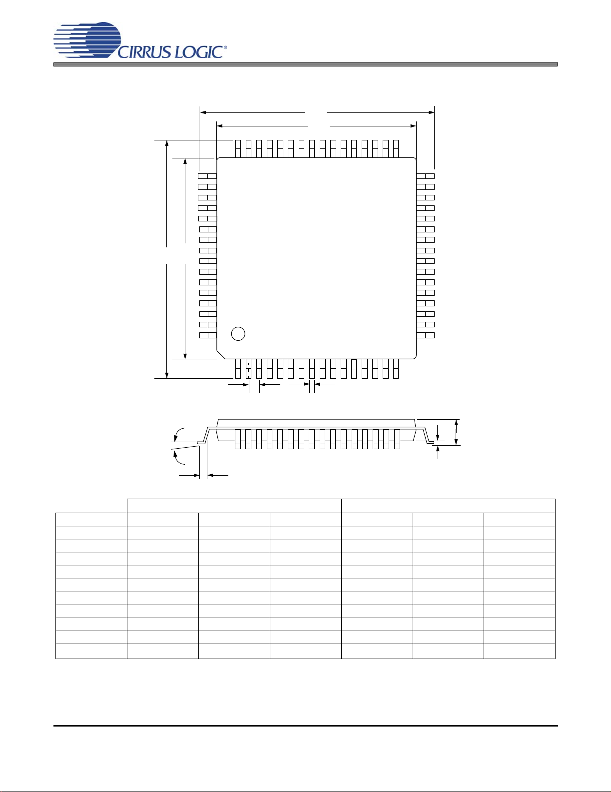
10.PACKAGE DIMENSIONS
64L LQFP PACKAGE DRAWING
D1
D
CS44600
E
E1
1
e
B
∝
Note: See Legend Below
A
A1
Figure 32. 64-Pin LQFP Package Drawing
L
INCHES MILLIMETERS
DIM MIN NOM MAX MIN NOM MAX
A --- 0.55 0.063 --- 1.40 1.60
A1 0.002 0.004 0.006 0.05 0.10 0.15
B 0.007 0.008 0.011 0.17 0.20 0.27
D 0.461 0.472 BSC 0.484 11.70 12.0 BSC 12.30
D1 0.390 0.39 3 BSC 0.398 9.9 0 10.0 BSC 10.10
E 0.461 0.472 BSC 0.484 11.70 12.0 BSC 12.30
E1 0.390 0.393 BSC 0.398 9.90 10.0 BSC 10.10
e* 0.016 0.020 BSC 0.024 0.40 0.50 BSC 0.60
L 0.018 0.024 0.030 0.45 0.60 0.75
∝
0.000° 4° 7.000° 0.00° 4° 7.00°
* Nominal pin pitch is 0.50 mmControlling dimension is mm.
JEDEC Designation: MS022
74 DS633F1
Page 75
11.THERMAL CHARACTERISTICS
Parameter Symbol Min Typ Max Units
Junction to Ambient Thermal Impedance 2 Layer Board
4 Layer Board
12.ORDERING INFORMATION
CS44600
θ
JA
-
-
48
38
-
°C/Watt
-
Product Description Package
CS44600
CS44600
CS44600
CS44600
CDB44800
CRD44800
CRD44800-ST-FB
CRD44600-PH-FB
6-Channel Digital Ampli-
fier Controller
6-Channel Digital Ampli-
fier Controller
6-Channel Digital Ampli-
fier Controller
6-Channel Digital Ampli-
fier Controller
CS44600/800 Evalua-
tion Board
8x50 W Half-Bridge
Reference Design Board
8x60 W Full-Bridge
Reference Design Board
2x100 W Full-Bridge
Reference Design Board
13.REVISION HISTORY
Pb-Free
LQFP YES -10° to +70°C Rail CS44600-CQZ
LQFP YES -10° to +70°C
LQFP YES -40° to +85°C Rail CS44600-DQZ
LQFP YES -40° to +85°C
- - - - CDB44800
- - - - CRD44800
- - - - CRD44800-ST-FB
- - - - CRD44600-PH-FB
Temp Range Container
Tape and
Reel
Tape and
Reel
Order#
CS44600-CQZR
CS44600-DQZR
Release Date Changes
-Updated “Features” on page 1
-Correcte “Power Supply Current” on page 9
-Corrected “High-Level Input Voltage” on page 9
-Corrected “Low-Level Input Voltage” on page 9
-Corrected “High-Level Output Voltage at Io = -2 mA” on page 9
PP1 May 2005
F1 March 2006 -Final Datasheet Release
DS633F1 75
-Corrected “Low-Level Output Voltage at Io = 2 mA” on page 9
-Corrected “Digital Filter Response (Note 12)” on page 11
-Updated “Typical Full-Bridge Connection Diagram” on page 22
-Updated “Typical Half-Bridge Connection Diagram” on page 23
-Corrected Figure 13 on page 23
-Updated Section 7.5.2 "AM Frequency Hopping (AM_FREQ_HOP)" on page 51
-Updated “Ordering Information” on page 75
Page 76

CS44600
Contacting Cirrus Logic Support
For all product questions and inquiries, contact a Cirrus Logic Sales Representative.
To find the one nearest to you, go to www.cirrus.com.
IMPORTANT NOTICE
Cirrus Logic, Inc. and its subsidiaries ("Cirrus") believe that the information contained in this document is accurate and reli able. However, the informatio n is subject
to change without notice and is prov ided "AS IS " without warrant y of any ki nd (expres s or impli ed). Custo mers are ad vised to obtai n the lat est ver sion of rel evant
information to verify, before placing orders, that informa tion be in g re lied on is c urr ent an d com pl ete. All prod ucts are sold subject to the terms and conditions of sale
supplied at the time of order acknowledgment, including those pertaining to warranty, indemnification, and limitation of liability. No responsibility is assumed by Cirrus
for the use of this information, including use of this information as the basis for manufacture or sale of any items, or for infringement of patents or other rights of third
parties. This document is the property of Cirrus and by furnishing this information, Cirrus grants no license, express or implied under any patents, mask work rights,
copyrights, trademarks, trade secrets or other intellectual proper ty rights. Cirrus owns th e copyrights associated with the information contained herein and gives consent for copies to be made of the information only for use within your organization with respect to Cirrus integrated circuits or other products of Cirrus. Th is co nse nt
does not extend to other copying such as copying for ge ne ral distribution, advertising or promotional purpo s es, or for cre atin g any wo rk for resale.
CERTAIN APPLICATIONS USING SEMICONDUCTOR PRODUCTS MAY INVOLVE POTENTIAL RISKS OF DEATH, PERSONAL INJURY, OR SEVERE PROPERTY OR ENVIRONMENTAL DAMAGE (“CRITICAL APPLICATIONS”). CIRRUS PRODUCTS ARE NOT DESIGNED, AUTHORIZED OR WARRANTED FOR USE
IN AIRCRAFT SYSTEMS, MILITARY APPLICATIONS, PRODUCTS SURGICALLY IMPLANTED INTO THE BODY, AUTOMOTIVE SAFETY OR SECURITY DEVICES, LIFE SUPPORT PRODUCTS OR OTHER CRITICAL APPLICATIONS. INCLUSION OF CIRRUS PRODUCTS IN SUCH APPLICATIONS IS UNDERSTOOD TO BE FULLY AT THE CUSTOMER’S RISK AND CIRRUS DISCLAIMS AND MAKES NO WARRANTY, EXPRESS, STATUTORY OR IMPLIED,
INCLUDING THE IMPLIED WARRANTIES OF MERCHANTABILITY AND FITNESS FOR PARTICULAR PURPOSE, WITH REGARD TO ANY CIRRUS PRODUCT
THAT IS USED IN SUCH A MANNER. IF THE CUSTOMER OR CUSTOMER’S CU STOMER USES O R PERMITS THE USE OF CIRRUS PRODUCTS IN CRITICAL
APPLICATIONS, CUSTOMER AGREES, BY SUCH USE, TO FULL Y INDE MNIFY CI RRUS, ITS OFF ICERS, DI RE CTORS , EMPLOY EES, DISTRIB UTORS AND
OTHER AGENTS FROM ANY AND ALL LIABILITY, INCLUDING ATTORNEYS’ FEES AND COSTS, THAT MAY RESULT FROM OR ARISE I N CONNECTION
WITH THESE USES.
Cirrus Logic, Cirrus, the Cirrus Logic logo designs, and Popguard are trademarks of Cirrus Logic, Inc. All other brand and product names in this document may be
trademarks or service marks of their respective owners.
SPI is a trademark of Motorola, Inc.
I²C is a registered tradem ar k of P h ilips Semiconductor.
76 DS633F1
 Loading...