

Page 1
1.8 V to 3.3 V
Multibit
Modulator
Charge
Pump
Left HP Out
Right HP Out
Serial Audio
Input
1.8 V to 2.5 V
PCM Serial Interface
Register
Configuration
Level Translator
Reset
Hardware
Mode or I
2
C &
SPI Software
Mode
Control Data
Beep
Generator
MUX
MUX
Headphone
Amp - GND
Centered
Headphone
Amp - GND
Centered
1.8 V to 2.5 V
Switched
Capacitor DAC
and Filter
Switched
Capacitor DAC
and Filter
Digital
Signal
Processing
Engine
CS43L21
Low-Power, Stereo Digital-to-Analog Converter
FEATURES
98 dB dynamic range (A-weighted)
-86 dB THD+N
Headphone amplifier–GND centered
– On-chip charge pump provides -VA_HP
– No DC-blocking capacitor required
– 46 mW power into stereo 16 @ 1.8 V
– 88 mW power into stereo 16 @ 2.5 V
– -75 dB THD+N
Digital signal processing engine
– Bass and treble tone control, de-emphasis
– PCM mix with independent volume control
– Master digital volume control and limiter
– Soft-ramp and zero-cross transitions
Beep generator
– Tone selections across two octaves
– Separate volume control
– Programmable On and Off time intervals
– Continuous, periodic, or one-shot beep
selections
Programmable peak-detect and limiter
Pop and click suppression
SYSTEM FEATURES
24-bit Conversion
4- to 96-kHz sample rate
Multibit delta–sigma architecture
Low power operation
– Stereo playback: 12.93 mW @ 1.8 V
Variable power supplies
– 1.8- to 2.5-V digital and analog
– 1.8- to 3.3-V interface logic
Power-down management
Software Mode (I²C™ and SPI™ control)
Hardware mode (standalone control)
Digital routing/mixes:
– Mono mixes
Flexible clocking options
– Master or slave operation
– High-impedance digital output option (for
easy MUXing between DAC and other data
sources)
– Quarter-speed mode (allows 8-kHz Fs
while maintaining a flat noise floor up to
16 kHz)
APPLICATIONS
Portable audio players
MD players
PDAs
Personal media players
Portable game consoles
Smart phones
Wireless headsets
http://www.cirrus.com
Copyright Cirrus Logic, Inc. 2013
(All Rights Reserved)
DS723F1
JAN ‘13
Page 2

CS43L21
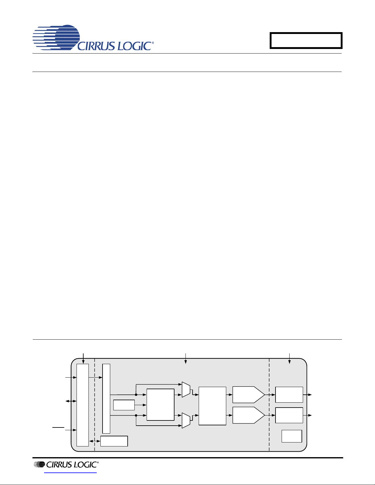
GENERAL DESCRIPTION
The CS43L21 is a highly integrated, 24-bit, 96 kHz, low power stereo DAC. Based on multi-bit, delta-sigma modulation, it allows infinite sample rate adju stm e nt be tw ee n 4 kH z an d 96 kHz. The DAC offers many features suit ab le
for low power, portable system applications.
The DAC output path includes a digital signal processing engine. Tone Control provides bass an d treble adjustment
of four selectable corner frequencies. The Mixer allows independent volume control for PCM mix, as well as a master digital volume control for the analog output. All volume level changes may be configured to occur on soft ramp
and zero cross transitions. The DAC also includes de-emphasis, limiting functions and a beep generator delivering
tones selectable across a range of two full octaves.
The stereo headphone amplifier is powered from a separate positive supply and the integrated charge pump provides a negative supply. This allows a ground-centered analog output with a wide signal swing and eliminates
external DC-blocking capacitors.
In addition to its many features, the CS43L21 operates from a low- voltage analog and digital core, makin g this DAC
ideal for portable systems that require extremely low power consumption in a minimal amount of space.
The CS43L21 is available in a 32-pin QFN package in both Commercial (-10 to +70° C) and Automotive grades (40 to +85° C). The CS43L21 Customer Demonstration b oa rd is a lso availa ble for d evice evaluation and imp leme ntation suggestions. Please see “Ordering Information” on page 64 for complete details.
2 DS723F1
Page 3

TABLE OF CONTENTS
1. PIN DESCRIPTIONS - SOFTWARE (HARDWARE) MODE .................................................................. 6
1.1 Digital I/O Pin Characteristics ........................................................................................................... 8
2. TYPICAL CONNECTION DIAGRAMS ................................................................................................... 9
3. CHARACTERISTIC AND SPECIFICATION TABLES ......................................................................... 11
SPECIFIED OPERATING CONDITIONS ............................................................................................. 11
ABSOLUTE MAXIMUM RATINGS .......................................................................................................11
ANALOG OUTPUT CHARACTERISTICS (COMMERCIAL - CNZ) ...................................................... 12
ANALOG OUTPUT CHARACTERISTICS (AUTOMOTIVE - DNZ) ................ ... ... .... ... ... ...................... 13
LINE OUTPUT VOLTAGE CHARACTERISTICS ................................................................................. 14
HEADPHONE OUTPUT POWER CHARACTERISTICS ................................... ... .... ... ... ... ... .... ... ... ... ... 15
COMBINED DAC INTERPOLATION & ON-CHIP ANALOG FILTER RESPONSE .............................. 16
SWITCHING SPECIFICATIONS - SERIAL PORT ............................................................................... 16
SWITCHING SPECIFICATIONS - I²C CONTROL PORT ..................................................................... 18
SWITCHING CHARACTERISTICS - SPI CONTROL PORT ................................................................ 19
DC ELECTRICAL CHARACTERISTICS .............................................................................................. 20
DIGITAL INTERFACE SPECIFICATIONS & CHARACTERISTICS ..................................................... 20
POWER CONSUMPTION .................................................................................................................... 21
4. APPLICATIONS ................................................................................................................................... 22
4.1 Overview ......................................................................................................................................... 22
4.1.1 Architecture ........................................................................................................................... 22
4.1.2 Line & Headphone Outputs ................................................................................................... 22
4.1.3 Signal Processing Engine ..................................................................................................... 22
4.1.4 Beep Generator ..................................................................................................................... 22
4.1.5 Device Control (Hardware or Software Mode) ...................................................................... 22
4.1.6 Power Management .............................................................................................................. 22
4.2 Hardware Mode .............................................................................................................................. 23
4.3 Analog Outputs ............................................................................................................................... 24
4.3.1 De-Emphasis Filter ................................................................................................................ 24
4.3.2 Volume Controls .................................................................................................................... 25
4.3.3 Mono Channel Mixer ............................................................................................................. 25
4.3.4 Beep Generator ..................................................................................................................... 25
4.3.5 Tone Control .......................................................................................................................... 26
4.3.6 Limiter .................................................................................................................................... 26
4.3.7 Line-Level Outputs and Filtering ........................................................................................... 27
4.3.8 On-Chip Charge Pump .......................................................................................................... 28
4.4 Serial Port Clocking ........................................................................................................................ 28
4.4.1 Slave ..................................................................................................................................... 29
4.4.2 Master ................................................................................................................................... 29
4.4.3 High-Impedance Digital Output ............................................................................................. 30
4.4.4 Quarter- and Half-Speed Mode .................................... .........................................................30
4.5 Digital Interface Formats ................................................................................................................ 30
4.6 Initialization ..................................................................................................................................... 31
4.7 Recommended Power-Up Sequence ............................................................................................. 31
4.8 Recommended Power-Down Sequence ........................................................................................ 32
4.9 Software Mode ............................................................................................................................... 34
4.9.1 SPI Control .............................................................................................................
4.9.2 I²C Control ............................................................................................................................. 34
4.9.3 Memory Address Pointer (MAP) ......................... .......... ......... .......... .......... ......... .......... ......... 36
4.9.3.1 Map Increment (INCR) ..................... ....... ...... ....... ...... ....... ...... ....... ...... ...... ....... ...... ... 36
5. REGISTER QUICK REFERENCE ........................................................................................................ 37
6. REGISTER DESCRIPTION .................................................................................................................. 40
6.1 Chip I.D. and Revision Register (Address 01h) (Read Only) ......................................................... 40
CS43L21
............... 34
DS723F1 3
Page 4

CS43L21
6.2 Power Control 1 (Address 02h) ...................................................................................................... 40
6.3 Speed Control (Address 03h) ......................................................................................................... 41
6.4 Interface Control (Address 04h) ..................................................................................................... 42
6.5 DAC Output Control (Address 08h) ................................................................................................ 42
6.6 DAC Control (Address 09h) ............................................................................................................ 43
6.7 PCMX Mixer Volume Control:
PCMA (Address 10h) & PCMB (Address 11h) ..................................................................................... 45
6.8 Beep Frequency & Timing Configuration (Address 12h) ................................................................ 46
6.9 Beep Off Time & Volume (Address 13h) ........................................................................................ 46
6.10 Beep Configuration & Tone Configuration (Address 14h) ... ......................................................... 48
6.11 Tone Control (Address 15h) ......................................................................................................... 49
6.12 AOUTx Volume Control:
AOUTA (Address 16h) & AOUTB (Address 17h) ................................................................................. 49
6.13 PCM Channel Mixer (Address 18h) .............................................................................................. 50
6.14 Limiter Threshold SZC Disable (Address 19h) ............................................................................. 51
6.15 Limiter Release Rate Register (Address 1Ah) .............................................................................. 52
6.16 Limiter Attack Rate Register (Address 1Bh) ................................................................................. 53
6.17 Status (Address 20h) (Read Only) ............................................................................................... 53
6.18 Charge Pump Frequency (Address 21h) ...................................................................................... 54
7. ANALOG PERFORMANCE PLOTS .......... ... .... ... ... ... .... ... ... ... .... ... ... .......................................... ... ... ...55
7.1 Headphone THD+N versus Output Power Plots ............................................................................ 55
7.2 Headphone Amplifier Efficiency ................................................................................................ ...... 57
8. EXAMPLE SYSTEM CLOCK FREQUENCIES .................................................................................... 58
8.1 Auto Detect Enabled ....................................................................................................................... 58
8.2 Auto Detect Disabled ...................................................................................................................... 59
9. PCB LAYOUT CONSIDERATIONS ..................................................................................................... 60
9.1 Power Supply, Grounding ............................................................................................................... 60
9.2 QFN Thermal Pad .......................................................................................................................... 60
10. DIGITAL FILTERS .............................................................................................................................. 61
11. PARAMETER DEFINITIONS .............................................................................................................. 62
12. REFERENCES .................................................................................................................................... 62
13. PACKAGE DIMENSIONS ............................................................................................................. 63
THERMAL CHARACTERISTICS .......................................................................................................... 63
14. ORDERING INFORMATION ............................................................................................................. 64
15. REVISION HISTORY ......................................................................................................................... 64
LIST OF FIGURES
Figure 1.Typical Connection Diagram (Software Mode) ............................................................................. 9
Figure 2.Typical Connection Diagram (Hardware Mode) .......................................................................... 10
Figure 3.Headphone Output Test Load ..................................................................................................... 15
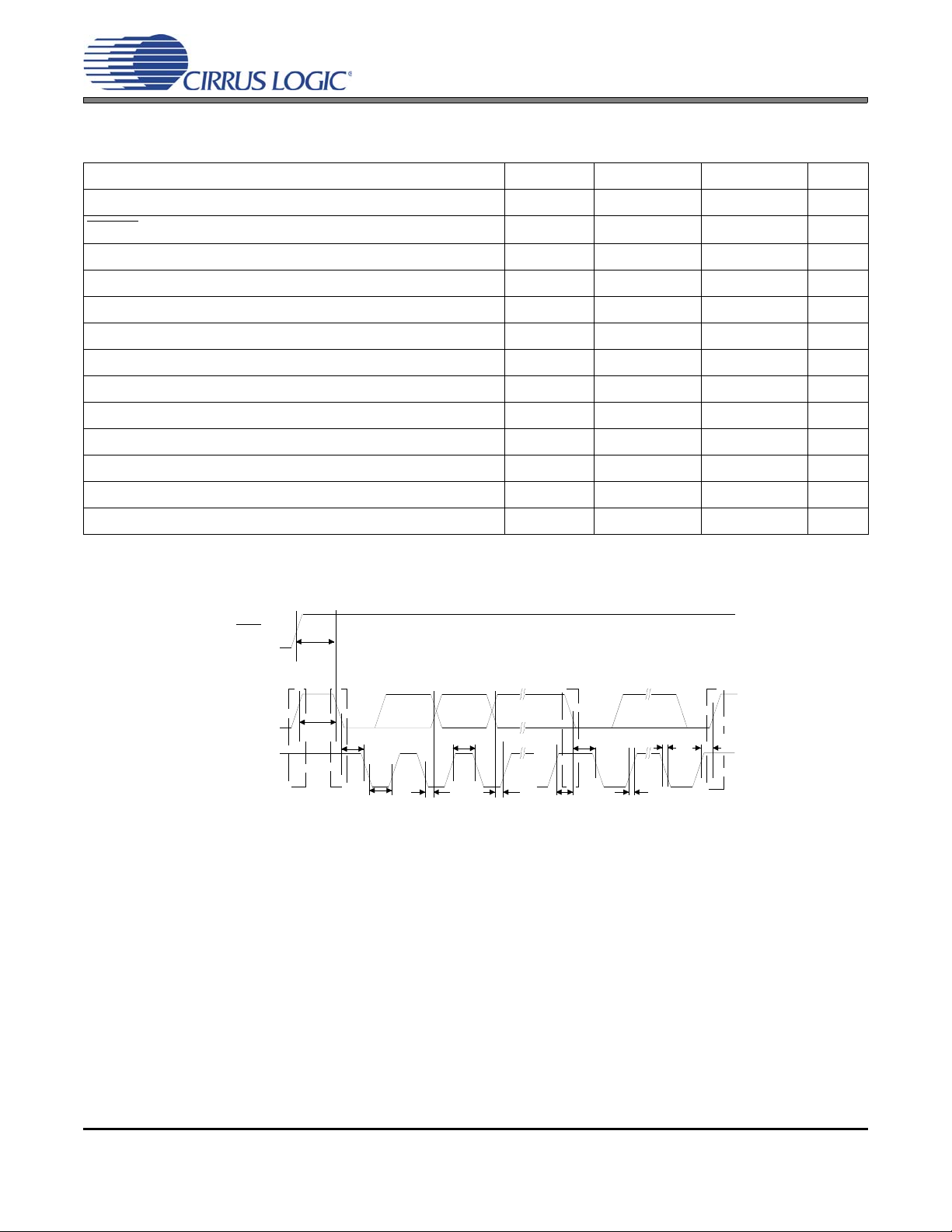
Figure 4.Serial Audio Interface Slave Mode Timing ..................... .......................................... ................... 17
Figure 5.Serial Audio Interface Master Mode Timing ....................................... ... ... ... .... ... ... ... ... .... ... ... ...... 17
Figure 6.Control Port Timing - I²C ... ... .... ... ... ... ... .......................................... .... ... ... ... .... ... ... ... ................... 18
Figure 7.Control Port Timing - SPI Format ............................. ... ... .... ... ... ... ................................................ 19
Figure 8.Output Architecture ..................................................................................................................... 24
Figure 9.De-Emphasis Curve .................................... ... ... .... ... ... ... .... ... ... ... ... .... ... ... ... .... ... ......................... 25
Figure 10.Beep Configuration Options ...................................................................................................... 26
Figure 11.Peak Detect & Limiter ............................................................................................................... 27
Figure 12.Master Mode Timing .................... ... ... .... ... ... ... .... ... ... ... .... ... ... ... ................................................ 29
Figure 13.Tri-State SCLK/LRCK .................. ... ... ....................................................................................... 30
Figure 14.I²S Format ............. .... ... ... ... .... ... .......................................... ... ... ... .... ... ... ... .... ... ......................... 30
Figure 15.Left-Justified Format .............. ... ... ... ... .... ... ... ... .... ... ... ... .... ......................................................... 31
Figure 16.Right-Justified Format (DAC only) ..... .... ... ... ... .... ... ... ... .... ... ... ... ... .... ......................................... 31
Figure 17.Initialization Flow Chart ................................ .......................................... ................................... 33
4 DS723F1
Page 5

Figure 18.Control Port Timing in SPI Mode .............................. ... .... ... ... ... ... .... ... ...................................... 34
Figure 19.Control Port Timing, I²C Write ................................................................................................... 35
Figure 20.Control Port Timing, I²C Read ................................................................................................... 35
Figure 21.THD+N vs. Output Power per Channel at 1.8 V (16 load) .................................................... 55
Figure 22.THD+N vs. Output Power per Channel at 2.5 V (16 load) .................................................... 55
Figure 23.THD+N vs. Output Power per Channel at 1.8 V (32 load) .................................................... 56
Figure 24.THD+N vs. Output Power per Channel at 2.5 V (32 load) .................................................... 56
Figure 25.Power Dissipation vs. Output Power into Stereo 16
Figure 26.Power Dissipation vs. Output Power into Stereo 16 (Log Detail) .... ... ... .... ... ......................... 57
Figure 27.Passband Ripple ....................................................................................................................... 61
Figure 28.Stopband ................................................................................................................................... 61
Figure 29.Transition Band ......................................................................................................................... 61
Figure 30.Transition Band (Detail) ............................................................................................................ 61
LIST OF TABLES
Table 1. I/O Power Rails ............................................................................................................................. 8
Table 2. Hardware Mode Feature Summary ............................................................................................. 23
Table 3. MCLK/LRCK Ratios .................... ... ... ... .... ... .......................................... ... ... .... ... ... ...................... 29
CS43L21
DS723F1 5
Page 6
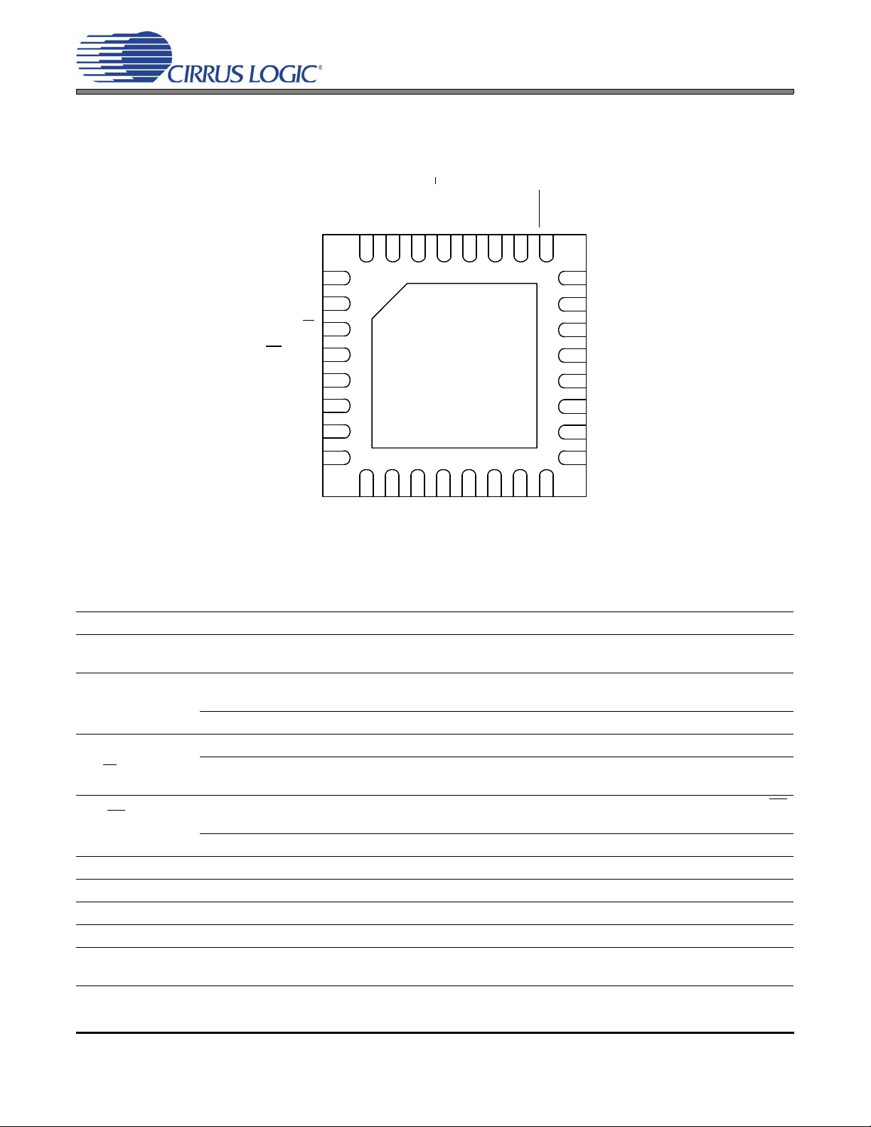
1. PIN DESCRIPTIONS - SOFTWARE (HARDWARE) MODE
109
8
7
6
5
4
3
2
1
11
12
13 14 15 16
17
18
19
20
21
22
23
24
25
262728
29
303132
CS43L21
VD
DGND
TSTO(M/S
)
MCLK
SDIN
SCLK
VSS_HP
AOUTB
AOUTA
VA
AGND
FILT+
NIC
VQ
SDA/CDIN (MCLKDIV2)
SCL/CCLK (I²S/LJ
)
ADO/CS
(DEM)
FLYP
VL
RESET
GND_HP
FLYN
TSTO
TSTO
TSTO
TSTO
TSTO
TSTO
TSTO
TSTO
VA_HP
LRCK
CS43L21
Pin Name # Pin Description
Left Right Clock (Input/Output) - Determines which channel, Left or Right, is currently active on the
LRCK
SDA/CDIN
(MCLKDIV2)
SCL/CCLK
)
(I²S/LJ
AD0/CS
(DEM)
VA_HP
FLYP
GND_HP
FLYN
VSS_HP
6 DS723F1
1
serial audio data line.
Serial Control Data (Input/Output) - SDA is a data I/O in I²C Mode. CDIN is the input data line for the
control port interface in SPI Mode.
2
MCLK Divide by 2 (Input) - Hardware Mode: Divides the MCLK by 2 prior to all internal circuitry.
Serial Control Port Clock (Input) - Serial clock for the serial control port.
3
Interface Format Selection (Input) - Hardware Mode: Selects between I²S & Left-Justified interface for-
mats for the DAC.
Address Bit 0 (I²C) / Control Port Chip Select (SPI) (Input) - AD0 is a chip address pin in I²C Mode; CS
is the chip-select signal for SPI format.
4
De-Emphasis (Input) - Hardware Mode: Enables/disables the de-emphasis filter.
5
Analog Power For Headphone (Input) - Positive power for the internal analog headphone section.
6
7
8
9
Charge Pump Cap Positive Node (Input) - Positive node for the external charge pump capacitor.
Analog Ground (Input) - Ground reference for the internal headphone/charge pump section.
Charge Pump Cap Negative Node (Input) - Negative node for the external charge pump capacitor.
Negative Voltage From Charge Pump (Output) - Negative voltage rail for the internal analog head-
phone section.
Page 7
CS43L21
AOUTB
AOUTA
VA
AGND
FILT+
VQ
NIC
TSTO
TSTO
TSTO
TSTO
TSTO
TSTO
RESET
VL
VD
DGND
TSTO
(M/S
)
MCLK
SCLK
SDIN
Thermal Pad
10
Analog Audio Output (Output) - The full-scale output level is specified in the DAC Analog Characteris-
11
tics specification table
12
Analog Power (Input) - Positive power for the internal analog section.
13
Analog Ground (Input) - Ground reference for the internal analog section.
14
Positive Voltage Reference (Output) - Positive reference voltage for the internal sampling circuits.
15
Quiescent Voltage (Output) - Filter connection for internal quiescent voltage.
Not Internally Connected - This pin is not connected internal to the device and may be connected to
16
ground or left “floating”. No other external connection should be made to this pin.
Test Out (Output) - This pin is an output used for test purposes only and must be left “floating” (no con-
17
nection external to the pin).
Test Out (Output) - This pin is an output used for test purposes only and must be left “floating” (no con-
18
nection external to the pin).
Test Out (Output) - This pin is an output used for test purposes only and must be left “floating” (no con-
19
nection external to the pin).
Test Out (Output) - This pin is an output used for test purposes only and must be left “floating” (no con-
20
nection external to the pin).
21
Test Out (Output) - This pin is an output used for test purposes only and must be left “floating” (no con-
22
nection external to the pin).
23
Test Out (Output) - This pin is an output used for test purposes only and must be left “floating” (no con-
24
nection external to the pin).
25
Reset (Input) - The device enters a low power mode when this pin is driven low.
Digital Interface Power (Input) - Determines the required signal level for the serial audio interface and
26
host control port. Refer to the Recommended Operating Conditions for appropriate voltages.
27
Digital Power (Input) - Positive power for the internal digital section.
28
Digital Ground (Input) - Ground reference for the internal digital section.
Test Out (Output) - This pin is an output used for test purposes only and must be left “floating” (no con-
nection external to the pin).
29
Serial Port Master/Slave (Input/Output) - Hardware Mode Startup Option: Selects between Master and
Slave Mode for the serial port.
30
Master Clock (Input) - Clock source for the delta-sigma modulators.
31
Serial Clock (Input/Output) - Serial clock for the serial audio interface.
32
Serial Audio Data Input (Input) - Input for two’s complement serial audio data.
-
Thermal relief pad for optimized heat dissipation. See “QFN Thermal Pad” on page 60.
DS723F1 7
Page 8
1.1 Digital I/O Pin Characteristics
The logic level for each input should not exceed the maximum ratings for the VL power supply.
CS43L21
Pin Name
SW/(HW)
RESET Input
SCL/CCLK
(I²S/LJ)
SDA/CDIN
(MCLKDIV2)
AD0/CS
(DEM)
MCLK Input
LRCK Input/Output
SCLK Input/Output
TSTO
(M/S)
SDIN Input
Input
Input/Output
Input
Input/Output
I/O Driver Receiver
- 1.8 V - 3.3 V
- 1.8 V - 3.3 V, with Hysteresis
1.8 V - 3.3 V, CMOS/Open Drain 1.8 V - 3.3 V, with Hysteresis
- 1.8 V - 3.3 V
- 1.8 V - 3.3 V
1.8 V - 3.3 V, CMOS 1.8 V - 3.3 V
1.8 V - 3.3 V, CMOS 1.8 V - 3.3 V
1.8 V - 3.3 V, CMOS 1.8 V - 3.3 V
- 1.8 V - 3.3 V
Table 1. I/O Power Rails
8 DS723F1
Page 9
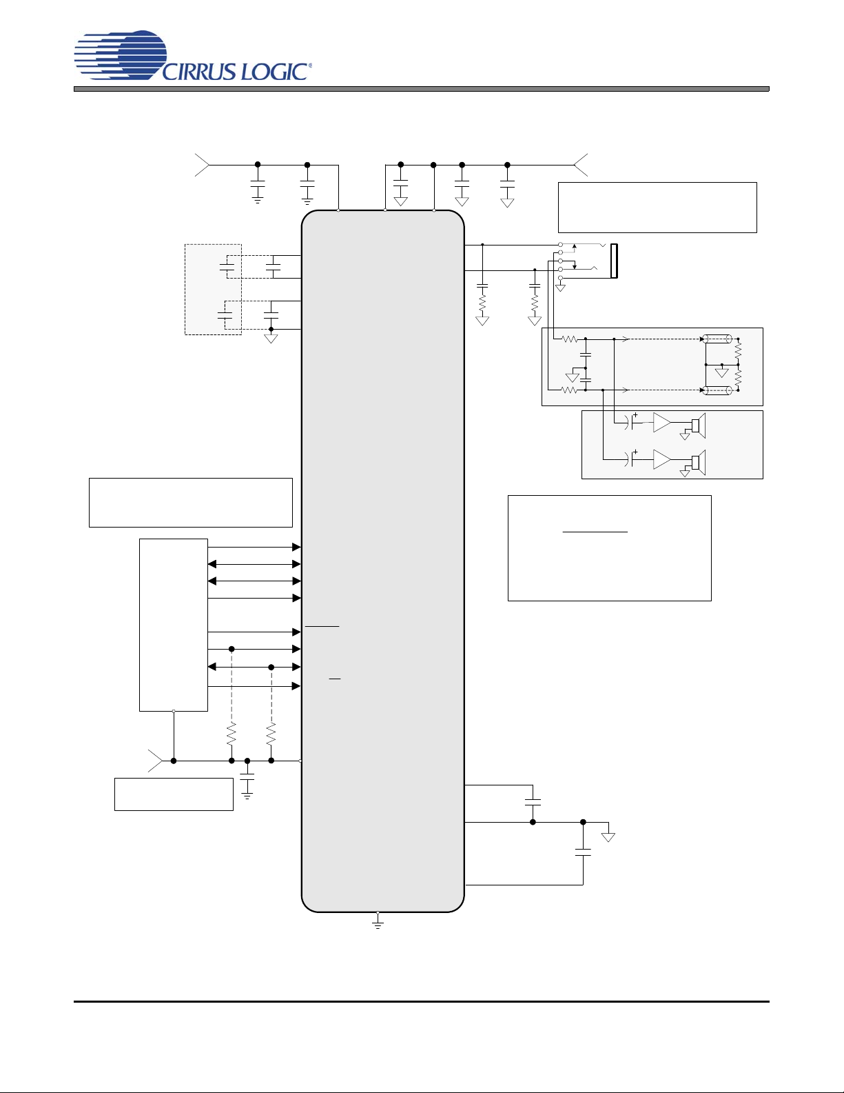
2. TYPICAL CONNECTION DIAGRAMS
1 µF
+1.8 V or +2.5 V
1 µF
VQ
FILT+
0.1 µF
1 µF
DGND
VL
0.1 µF
+1.8 V, +2.5 V
or +3.3 V
SCL/CCLK
SDA/CDIN
RESET
2 k
See Note 1
LRCK
AGND
AD0/CS
MCLK
SCLK
0.1 µF
VA_HP
VD
SDIN
CS43L21
2 k
1 µF
+1.8 V or +2.5 V
AOUTB
AOUTA
470
470
C
C
R
ext
R
ext
See Note 2
Note 1:
Resistors are required for I²C
control port operation
For best response to Fs/2 :
4704
470
ext
ext
RFs
R
C
This circuitry is intended for applications where the
CS43L21 connects directly to an unbalanced output of the
device. For internal routing applications please see the
DAC Analog Output Characteristics section for loading
limitations.
Note 2 :
Digital Audio
Processor
0.1 µF
VA
Headphone Out
Left & Right
Line Level Out
Left & Right
Speaker Driver
FLYP
FLYN
VSS_HP
GND_HP
1 µF
51.1
0.022 µF
1 µF
**
**
* *Use low ESR ceramic capacitors.
See Note 3
Note 3:
Series resistance in the path of the power supplies must
be avoided. Any voltage drop on VA_HP will directly
impact the negative charge pump supply (VSS_HP) and
result in clipping on the audio output .
1.5 µF
1.5 µF
See Note 4
Note 4 :
Larger capacitors, such as 1.5 µF, improves the charge
pump performance (and subsequent THD+N) at the full
scale output power achieved with gain (G) settings
greater than default.
**
**
Figure 1. Typical Connection Diagram (Software Mode)
CS43L21
DS723F1 9
Page 10
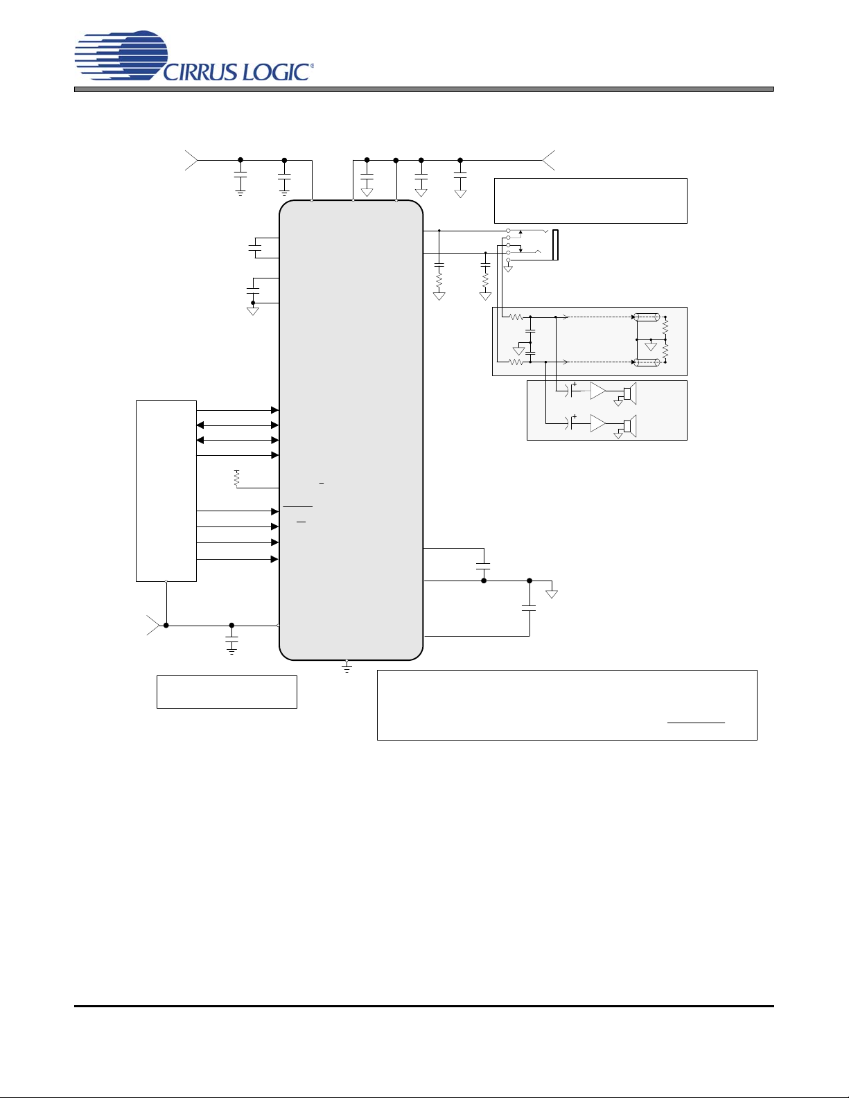
CS43L21
+1.8V or +2.5V
1 µF
VQ
FILT+
0.1 µF
1 µF
DGND
VL
0.1 µF
+1.8V, 2.5 V
or +3.3V
I²S/LJ
MCLKDIV2
RESET
LRCK
AGND
DEM
MCLK
SCLK
0.1 µF
VA_HP
VD
SDIN
CS43L21
1 µF
+1.8V or +2.5V
AOUTB
AOUTA
470
470
C
C
R
ext
R
ext
See Note 2
For best response to Fs/2 :
4704
470
ext
ext
RFs
R
C
This circuitry is intended for applications where the CS43L21 connects directly to an unbalanced output of the device . For
internal routing applications please see the DAC Analog Output Characteristics section for loading limitations .
Note 2 :
Digital Audio
Processor
0.1 µF
VA
Headphone Out
Left & Right
Line Level Out
Left & Right
Speaker Driver
FLYP
FLYN
VSS_HP
GND_HP
51.1
0.022 µF
1 µF
See Note 1
Note 1:
Series resistance in the path of the power supplies (typically
used for added filtering) must be avoided. Any voltage drop
on VA_HP will directly impact the negative charge p ump
supply (VSS_HP) and result in clipping on the audio output.
1 µF
1 µF
**
**
* *Use low ESR ceramic capacitors.
See Note 3
Note 3:
Pull-up to VL (47 kfor Master Mode. Pull-
down to DGND for Slave Mode.
47k
TSTO/M/S
VL or DGND
k
Figure 2. Typical Connection Diagram (Hardware Mode)
10 DS723F1
Page 11
CS43L21
3. CHARACTERISTIC AND SPECIFICATION TABLES
(All Min/Max characteristics and specifications are guaranteed over the Specified Operating Conditions. Typical performance characteristics and specifications are derived from measurements taken at nominal supply voltages and
T
= 25° C.)
A
SPECIFIED OPERATING CONDITIONS
(AGND=DGND=0 V, all voltages with respect to ground.)
Parameters Symbol Min Max Units
DC Power Supply (Note 1)
Analog Core
Headphone Amplifier
Digital Core
Serial/Control Port Interface
Ambient Temperature Commercial - CNZ
Automotive - DNZ
VA 1.65 2.63 V
VA_HP 1.65 2.63 V
VD 1.65 2.63 V
VL 1.65 3.47 V
T
A
-10
-40
+70
+85
C
C
ABSOLUTE MAXIMUM RATINGS
(AGND = DGND = 0 V; all voltages with respect to ground.)
Parameters Symbol Min Max Units
DC Power Supply Analog
Digital
Serial/Control Port Interface
Input Current (Note 2)
External Voltage Applied to Analog Output
External Voltage Applied to Digital Input (Note 3) V
Ambient Operating Temperature (power applied)
Storage Temperature
VA, VA_HP
VD
VL
V
T
T
I
in
IN
IND
A
stg
-0.3
-0.3
-0.3
-±10mA
-VA_HP - 0.3 +VA_HP + 0.3
-0.3 VL+ 0.3 V
-50 +115 °C
-65 +150 °C
3.0
3.0
4.0
V
V
V
V
WARNING:Operation at or beyo nd these limits may result in permanent damage to the device. Normal operation
is not guaranteed at these extremes.
Notes:
1. The device will operate properly over the full range of the analog, headphone amplifier, digital core and
serial/control port interface supplies.
2. Any pin except supplies. Transient currents of up to ±100 mA on the analog input pins will not cause
SCR latch-up.
3. The maximum over/under voltage is limited by the input current.
DS723F1 11
Page 12
CS43L21
ANALOG OUTPUT CHARACTERISTICS (COMMERCIAL - CNZ)
(Test conditions (unless otherwise specified): Input test signal is a full-scale 997 Hz sine wave; measurement
bandwidth is 10 Hz to 20 kHz; Sample Frequency = 48 kHz; test load R
(see Figure 3), and test load R
= 16 CL = 10 pF (see Figure 3) for the headphone output. HP_GAIN[2:0] = 011.)
L
= 10 k CL = 10 pFfor the line output
L
Parameter (Note 4)
R
= 10 k
L
Dynamic Range
18 to 24-Bit A-weighted
unweighted
16-Bit A-weighted
unweighted
Total Harmonic Distortion + Noise
18 to 24-Bit 0 dB
-20 dB
-60 dB
16-Bit 0 dB
-20 dB
-60 dB
RL = 16
Dynamic Range
18 to 24-Bit A-weighted
unweighted
16-Bit A-weighted
unweighted
Total Harmonic Distortion + Noise
18 to 24-Bit 0 dB
-20 dB
-60 dB
16-Bit 0 dB
-20 dB
-60 dB
Other Characteristics for RL = 16 or 10 k
Output Parameters Modulation Index (MI)
(Note 5) Analog Gain Multiplier (G)
Full-scale Output Voltage (2•G•MI•VA) (Note 5)
Full-scale Output Power (Note 5)
Interchannel Isolation (1 kHz) 16
Interchannel Gain Mismatch
Gain Drift
AC-Load Resistance (R
Load Capacitance (C
) (Note 6)
L
) (Note 6)
L
10 k
VA = 2.5V (nominal)
Min Typ Max
92
89
-
-
-
-
-
-
-
-
92
89
-
-
-
-
-
-
-
-
-
Refer to Table “Line Output Voltage Characteristics” on
Refer to Table “Headphone Output Power Characteristics”
-
-
- 0.1 0.25 - 0.1 0.25 dB
- ±100 - - ±100 -
16 - - 16 - -
- - 150 - - 150 pF
98
95
96
93
-86
-75
-35
-86
-73
-33
98
95
96
93
-75
-75
-35
-75
-73
-33
0.6787
0.6047
80
95
-
-
-
-
-78
-
-
-
-
-
-
-
-
-
-69
-
-
-
-
-
--
page 14
on page 15
-
-
VA = 1.8V (nominal)
Min Typ Max Unit
89
86
-
-
-
-
-
-
-
-
89
86
-
-
-
-
-
-
-
-
-
-
95
92
93
90
-88
-72
-32
-88
-70
-30
95
92
93
90
-75
-72
-32
-75
-70
-30
0.6787
0.6047
80
93
-
-
-
-
-82
-
-
-
-
-
-
-
-
-
-69
-
-
-
-
-
-
-
-
dB
dB
dB
dB
dB
dB
dB
dB
dB
dB
dB
dB
dB
dB
dB
dB
dB
dB
dB
dB
Vpp
mW
dB
dB
ppm/°
C
12 DS723F1
Page 13
CS43L21
ANALOG OUTPUT CHARACTERISTICS (AUTOMOTIVE - DNZ)
(Test conditions (unless otherwise specified): Input test signal is a full-scale 997 Hz sine wave; measurement
bandwidth is 10 Hz to 20 kHz; Sample Frequency = 48 kHz and 96 kHz; test load R
line output (see Figure 3), and test load R
= 16 CL = 10 pF (see Figure 3) for the headphone output.
L
HP_GAIN[2:0] = 011.)
= 10 k CL = 10 pFfor the
L
Parameter (Note 4)
R
= 10 k
L
Dynamic Range
18 to 24-Bit A-weighted
unweighted
16-Bit A-weighted
unweighted
Total Harmonic Distortion + Noise
18 to 24-Bit 0 dB
-20 dB
-60 dB
16-Bit 0 dB
-20 dB
-60 dB
RL = 16
Dynamic Range
18 to 24-Bit A-weighted
unweighted
16-Bit A-weighted
unweighted
Total Harmonic Distortion + Noise
18 to 24-Bit 0 dB
-20 dB
-60 dB
16-Bit 0 dB
-20 dB
-60 dB
Other Characteristics for RL = 16 or 10 k
Output Parameters Modulation Index (MI)
(Note 5) Analog Gain Multiplier (G)
Full-scale Output Voltage (2•G•MI•VA) (Note 5)
Full-scale Output Power (Note 5)
Interchannel Isolation (1 kHz) 16
Interchannel Gain Mismatch
Gain Drift
AC-Load Resistance (R
Load Capacitance (C
) (Note 6)
L
) (Note 6)
L
10 k
VA = 2.5V (nominal)
Min Typ Max
90
87
-
-
-
-
-
-
-
-
90
87
-
-
-
-
-
-
-
-
-
Refer to Table “Line Output Voltage Characteristics” on
Refer to Table “Headphone Output Power Characteristics”
-
-
- 0.1 0.25 - 0.1 0.25 dB
- ±100 - - ±100 -
16 - - 16 - -
- - 150 - - 150 pF
98
95
96
93
-86
-75
-35
-86
-73
-33
98
95
96
93
-75
-75
-35
-75
-73
-33
0.6787
0.6047
80
95
-
-
-
-
-73
-
-
-
-
-
-
-
-
-
-67
-
-
-
-
-
--
page 14
on page 15
-
-
VA = 1.8V (nominal)
Min Typ Max Unit
87
84
-
-
-
-
-
-
-
-
87
84
-
-
-
-
-
-
-
-
-
-
95
92
93
90
-88
-72
-32
-88
-70
-30
95
92
93
90
-75
-72
-32
-75
-70
-30
0.6787
0.6047
80
93
-
-
-
-
-80
-
-
-
-
-
-
-
-
-
-67
-
-
-
-
-
-
-
-
dB
dB
dB
dB
dB
dB
dB
dB
dB
dB
dB
dB
dB
dB
dB
dB
dB
dB
dB
dB
Vpp
mW
dB
dB
ppm/°
C
DS723F1 13
Page 14
CS43L21
LINE OUTPUT VOLTAGE CHARACTERISTICS
Test conditions (unless otherwise specified): Input test signal is a full-scale 997 Hz sine wave; measurement bandwidth is 10 Hz to 20 kHz; Sample Frequency = 48 kHz; test load R
= 10 k CL = 10 pF (see Figure 3).
L
Parameter
AOUTx Voltage Into R
HP_GAIN[2:0]
000 0.3959
001 0.4571
010 0.5111
011 (default) 0.6047
100 0.7099
101 0.8399
110 1.0000
111 1.1430
Analog
Gain (G)
= 10 k
L
VA = 2.5V (nominal)
Min Typ Max
VA = 1.8V (nominal)
Min Typ Max Unit
VA_HP
1.8 V - 1.34 - - 0.97 - V
2.5 V - 1.34 - - 0.97 - V
1.8 V - 1.55 - - 1.12 - V
2.5 V - 1.55 - - 1.12 - V
1.8 V - 1.73 - - 1.25 - V
2.5 V - 1.73 - - 1.25 - V
1.8 V - 2.05 - 1.41 1.48 1.55 V
2.5 V 1.95 2.05 2.15 - 1.48 - V
1.8 V - 2.41 - - 1.73 - V
2.5 V - 2.41 - - 1.73 - V
1.8 V - 2.85 - 2.05 V
2.5 V - 2.85 - - 2.05 - V
1.8 V - 3.39 - - 2.44 - V
2.5 V - 3.39 - - 2.44 - V
1.8 V
2.5 V - 3.88 - - 2.79 - V
(See (Note 7) 2.79 V
pp
pp
pp
pp
pp
pp
pp
pp
pp
pp
pp
pp
pp
pp
pp
pp
14 DS723F1
Page 15
CS43L21
AOUTx
AGND
R
L
C
L
0.022 F
51
Figure 3. Headphone Output Test Load
HEADPHONE OUTPUT POWER CHARACTERISTICS
Test conditions (unless otherwise specified): Input test signal is a full-scale 997 Hz sine wave; measurement bandwidth is 10 Hz to 20 kHz; Sample Frequency = 48 kHz; test load R
= 16 CL = 10 pF (see Figure 3).
L
Parameter
AOUTx Power Into R
HP_GAIN[2:0]
000 0.3959
001 0.4571
010 0.5111
011 (default) 0.6047
100 0.7099
101 0.8399
110 1.0000
111 1.1430
Analog
Gain (G)
4. One LSB of triangular PDF dither is added to data.
5. Full-scale output voltage and power is determined by the gain setting, G, in register “Headphone Analog
Gain (HP_GAIN[2:0])” on page 42. High gain settings at certain VA and VA_HP supply levels may
cause clipping when the audio signal approaches full-scale, maximum power output, as shown in
Figures 21 - 24 on page 56.
6. See Figure 3. R
quired for the internal op-amp's stability and signal integrity. In this circuit topology, C
move the band-limiting pole of the amp in the output stage. Increasing this value beyond the recommended 150 pF can cause the internal op-amp to become unstable.
7. VA_HP settings lower than VA reduces the headroom of the headph one amplifier. As a result, the DAC
may not achieve the full THD+N performance at full-scale output voltage and power.
= 16
L
VA = 2.5V (nominal)
Min Typ Max
VA = 1.8V (nominal)
Min Typ Max Unit
VA_HP
1.8 V - 14 - - 7 - mW
2.5 V - 14 - - 7 - mW
1.8 V - 19 - - 10 - mW
2.5 V - 19 - - 10 - mW
1.8 V - 23 - - 12 - mW
2.5 V - 23 - - 12 - mW
1.8 V (Note 7) -17 -mW
2.5 V - 32 - - 17 - mW
1.8 V (Note 7) -23 -mW
2.5 V - 44 - - 23 - mW
1.8 V (Note 5) mW
2.5 V -32 -mW
1.8 V
2.5 V mW
(Note 5, 7)
1.8 V mW
2.5 V mW
and CL reflect the recommended minimum resistance and maximum capacitance re-
L
will effectively
L
mW
rms
rms
rms
rms
rms
rms
rms
rms
rms
rms
rms
rms
rms
rms
rms
rms
DS723F1 15
Page 16

CS43L21
COMBINED DAC INTERPOLATION & ON-CHIP ANALOG FILTER RESPONSE
Parameter
Frequency Response 10 Hz to 20 kHz
Passband to -0.05 dB corner
StopBand
StopBand Attenuation (Note 9)
Group Delay
De-emphasis Error Fs = 32 kHz
(Note 8) Min Typ Max Unit
to -3 dB corner
Fs = 44.1 kHz
Fs = 48 kHz
Notes:
8. Response is clock dependent and will scale with Fs. Note that the response plots (Figure 27 to Figure 30
on page 61) have been normalized to Fs and can be denormalized by multiplying the X-axis scale by Fs.
9. Measurement Bandwidth is from Stopband to 3 Fs.
SWITCHING SPECIFICATIONS - SERIAL PORT
(Inputs: Logic 0 = DGND, Logic 1 = VL.)
Parameters Symbol Min Max Units
RESET
MCLK Frequency
MCLK Duty Cycle (Note 11)
Slave Mode
Input Sample Rate (LRCK) Quarter-Speed Mode
LRCK Duty Cycle
SCLK Frequency
SCLK Duty Cycle
LRCK Setup Time Before SCLK Rising Edge
SDIN Setup Time Before SCLK Rising Edge
SDIN Hold Time After SCLK Rising Edge
pin Low Pulse Width (Not e 10)
Half-Speed Mode
Single-Speed Mode
Double-Speed Mode
-0.01 - +0.08 dB
0
0
0.5465 - - Fs
50 - - dB
- 10.4/Fs - s
-
-
-
F
s
F
s
F
s
F
s
1/t
P
t
s(LK-SK)
t
s(SD-SK)
t
h
-
-
-
-
-
1-ms
1.024 38.4 MHz
45 55 %
4
8
4
50
45 55 %
-64•FsHz
45 55 %
40 - ns
20 - ns
20 - ns
0.4780
0.4996
+1.5/+0
+0.05/-0.25
-0.2/-0.4
12.5
25
50
100
kHz
kHz
kHz
kHz
Fs
Fs
dB
dB
dB
16 DS723F1
Page 17
Master Mode (Note 12)
MCLK
128
-----------------
//
//
//
//
//
//
t
s(SD-SK)
MSB MSB-1
LRCK
SCLK
SDIN
t
s(LK-SK)
t
P
t
h
Figure 4. Serial Audio Interface Slave Mode Timing
//
//
//
//
//
//
t
s(SD-SK)
MSB MSB-1
LRCK
SCLK
SDIN
t
d(MSB)
t
P
t
h
Figure 5. Serial Audio Interface Master Mode Timing
CS43L21
Parameters Symbol Min Max Units
Output Sample Rate (LRCK) All Speed Modes
(Note 13)
LRCK Duty Cycle
SCLK Frequency
SCLK Duty Cycle
LRCK Edge to SDIN MSB Rising Edge
SDIN Setup Time Before SCLK Rising Edge
SDIN Hold Time After SCLK Rising Edge
10. After powering up the CS43L21, RESET should be held low after the power supplies and clocks are
settled.
11. See “Example System Clock Frequencies” on page 58 for typical MCLK frequencies.
12. See“Master” on page 29.
13. “MCLK” refers to the external master clock applied.
F
s
1/t
P
t
d(MSB)
t
s(SD-SK)
t
h
-Hz
45 55 %
- 64•F
s
Hz
45 55 %
52 ns
20 - ns
20 - ns
DS723F1 17
Page 18
SWITCHING SPECIFICATIONS - I²C CONTROL PORT
t
buf
t
hdst
t
hdst
t
low
t
r
t
f
t
hdd
t
high
t
sud
t
sust
t
susp
Stop Start
Start
Stop
Repeated
SDA
SCL
t
irs
RST
Figure 6. Control Port Timing - I²C
(Inputs: Logic 0 = DGND, Logic 1 = VL, SDA CL=30pF)
Parameter Symbol Min Max Unit
SCL Clock Frequency
RESET Rising Edge to Start
Bus Free Time Between Transmissions
Start Condition Hold Time (prior to first clock pulse)
Clock Low time
Clock High Time
Setup Time for Repeated Start Condition
SDA Hold Time from SCL Falling (Note 14)
SDA Setup time to SCL Rising
Rise Time of SCL and SDA
Fall Time SCL and SDA
Setup Time for Stop Condition
Acknowledge Delay from SCL Falling
f
t
t
t
hdst
t
low
t
high
t
sust
t
hdd
t
sud
t
t
t
susp
t
ack
scl
irs
buf
rc
fc
CS43L21
- 100 kHz
500 - ns
4.7 - µs
4.0 - µs
4.7 - µs
4.0 - µs
4.7 - µs
0-µs
250 - ns
-1µs
- 300 ns
4.7 - µs
300 3450 ns
14. Data must be held for sufficient time to bridge the transition time, t
, of SCL.
fc
18 DS723F1
Page 19
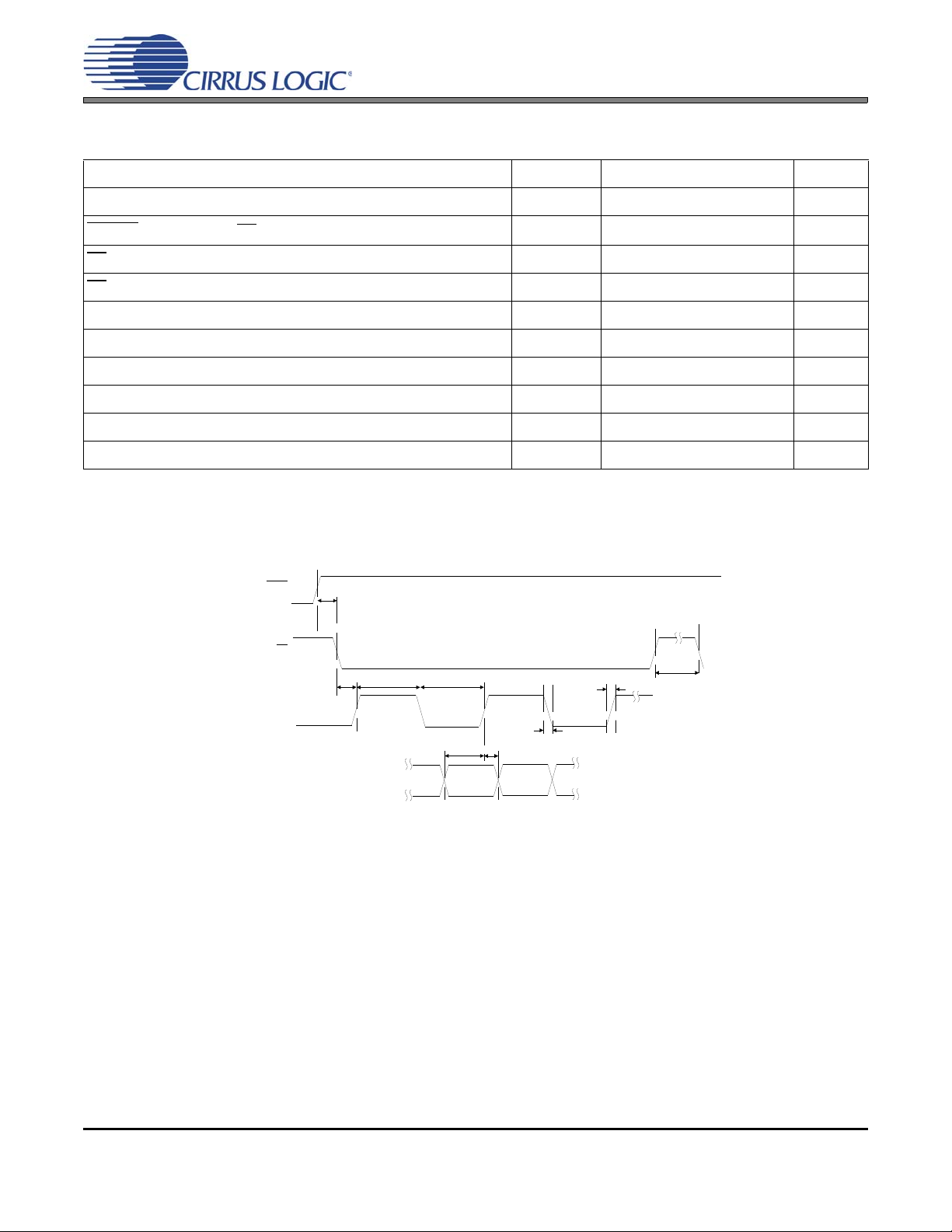
SWITCHING CHARACTERISTICS - SPI CONTROL PORT
CS
CCLK
CDIN
RST
t
srs
t
scl
t
sch
t
css
t
r2
t
f2
t
csh
t
dsu
t
dh
Figure 7. Control Port Timing - SPI Format
(Inputs: Logic 0 = DGN D, Lo gic 1 = VL)
Parameter Symbol Min Max Units
CS43L21
CCLK Clock Frequency
RESET Rising Edge to CS Falling
Falling to CCLK Edge
CS
CS
High Time Between Transmissions
CCLK Low Time
CCLK High Time
CDIN to CCLK Rising Setup Time
CCLK Rising to DATA Hold Time (Note 15)
Rise Time of CCLK and CDIN (Note 16)
Fall Time of CCLK and CDIN (Note 16)
15. Data must be held for sufficient time to bridge the transition time of CCLK.
16. For f
<1 MHz.
sck
f
t
t
t
t
sck
t
srs
css
csh
t
scl
sch
dsu
t
t
t
06.0MHz
20 - ns
20 - ns
1.0 - s
66 - ns
66 - ns
40 - ns
dh
r2
f2
15 - ns
-100ns
-100ns
DS723F1 19
Page 20
DC ELECTRICAL CHARACTERISTICS
(AGND = 0 V; all voltages with respect to ground.)
Parameters Min Typ Max Units
VQ Characteristics
Nominal Voltage
Output Impedance
DC Current Source/Sink (Note 17)
FILT+
-
-
-
-VA-V
0.5•VA
23
-
VSS_HP Characteristics
Nominal Voltage
DC Current Source
Power Supply Rejection Ratio (PSRR) (Note 18) 1 kHz
-
-
-60-dB
-0.8•(VA_HP) -
17. The DC current draw represents the allowed current draw from the VQ pin due to typical leakage
through electrolytic de-coupling capacitors.
18. Valid with the recommended capacitor values on FILT+ and VQ. Increasing the capacitance will also
increase the PSRR.
DIGITAL INTERFACE SPECIFICATIONS & CHARACTERISTICS
Parameters (Note 19) Symbol Min Max Units
Input Leakage Current
Input Capacitance
1.8 V - 3.3 V Logic
High-Level Output Voltage (I
Low-Level Output Voltage
High-Level Input Voltage
Low-Level Input Voltage
= -100 A)
OH
(IOL = 100 A)
I
in
V
OH
V
OL
V
IH
V
IL
-±10A
-10pF
VL - 0.2 - V
-0.2V
0.68•VL - V
- 0.32•VL V
CS43L21
-
-
10
10
V
k
A
V
A
19. See “Digital I/O Pin Characteristics” on page 8 for serial and control port power rails.
20 DS723F1
Page 21
POWER CONSUMPTION
See (Note 20)
Power Control Registers Typical Current (mA)
02h 03h
Operation
PDN_DACB
PDN_DACA
BIT 4
BIT 3
BIT 2
BIT 1
PDN
BIT 3
BIT 2
1
Off
(Note 21)
2 Standby (Note 22)
5 Mono Playback 1011110111
6 Stereo Playback
20. Unless otherwise noted, test conditions are as follows: All zeros input, slave mode, sample rate =
48 kHz; No load. Digital (VD) and logic (VL) supply current will vary depending on speed mode and master/slave operation.
21. RESET
22. RESET
pin 25 held LO, all clocks and data lines are held LO.
pin 25 held HI, all clocks and data lines are held HI.
23. VL current will slightly increase in master mode.
xxxxxxxxxx
xxxxxx1xxx
0011110111
CS43L21
i
i
VA_HP
V
BIT 1
1.8 0 0 0 0 0
2.5 0 0 0 0 0
1.8 0 0.01 0.02 0 0.05
2.5 0 0.01 0.03 0 0.10
1.8 1.66 1.40 2.35 0.01 9.74
2.5 2.03 1.71 3.48 0.02 18.08
1.8 2.77 2.05 2.35 0.01 12.93
2.5 3.21 2.50 3.49 0.02 23.02
i
VA
i
VD
VL
(Note
23)
Total
Power
(mW
rms
)
DS723F1 21
Page 22

4. APPLICATIONS
4.1 Overview
4.1.1 Architecture
The CS43L21 is a highly integrated, low power, 24-bit audio D/A comprised of stereo digital-to-analog
converters (DAC) designed using multi-bit delta-sigma techni ques. The DAC operates at an oversamp ling
ratio of 128 Fs. The D/A operates in one of four sample ra te speed modes: Quarter , Half, Single and Double. It accepts and is capable of generating serial port cl ocks (SCLK, LRCK) derived from an input Master
Clock (MCLK).
4.1.2 Line & Headphone Outputs
The analog output portion of the D/A includes a headphone amplifier capable of driving headphone and
line-level loads. An on-chip charge pump creates a negative headphone supply allowing a full-scale output swing centered around ground. This eliminates the need for large DC-Blocking capacitors and allows
the amplifier to deliver more power to headphone loads at lower supply voltages. Eight gain settings for
the headphone amplifier are available.
4.1.3 Signal Processing Engine
A signal processing engine is available to process serial input D/A data be fore output to the DAC. The
D/A data has independent volume controls and mixing functions such as mo no mixes a nd left/right cha nnel swaps. A Tone Control provides bass and treble at four selectable corner frequencies. An automatic
level control provides limiting capabilities at programmable attack and release rates, maximum thresholds
and soft ramping. A 15/50 s de-emphasis filter is also available at a 44.1 kHz sample rate.
CS43L21
4.1.4 Beep Generator
A beep may be generated internally at select frequencies across approximately two octave major scales
and configured to occur continuously, periodically or at single time interva ls controlled by the user. Volume
may be controlled independently.
4.1.5 Device Control (Hardware or Software Mode)
In Software Mode, all functions and features may be controlled via a two-wire I²C or three-wire SPI control
port interface. In Hardware Mode, a limited feature set may be controlled via stand-alone control pins.
4.1.6 Power Management
Two Software Mode control registers provid e independen t power-down control of the DAC, allo wing operation in select applications with minimal power consumption.
22 DS723F1
Page 23

4.2 Hardware Mode
A limited feature-set is available when the D/A powers up in Hardware Mode (see “Recommended Power-
Up Sequence” section on page 31) and may be controlled via stand-alone control pins. Table 2 shows a list
of functions/features, the default configuration and the associated stand-alone control available.
Hardware Mode Feature/Function Summary
Feature/Function Default Configuration Stand-Alone Control Note
Power Control Device
DACx
Auto-Detect
Speed Mode Serial Port Slave
Serial Port Master
MCLK Divide
Serial Port Master / Slave Selection
Interface Control DAC
DAC Volume & Gain HP Gain
AOUTx Volume
Invert
Soft Ramp
Zero Cross
DAC De-Emphasis
Signal Processing Engine (SPE) Mix
Beep
Tone Control
Peak Detect and Limiter
Data Selection
Channel Mix DAC
Charge Pump Frequency
Table 2. Hardware Mode Feature Summary
CS43L21
Powered Up
Powered Up
Enabled - -
Auto-Detect Speed Mode
Single-Speed Mode
(Selectable) “MCLKDIV2” pin 2
(Selectable) “M/S” pin 29
(Selectable) “I²S/LJ” pin 3
G = 0.6047
0 dB
Disabled
Enabled
Disabled
(Selectable) “DEM” pin 4
Disabled
Disabled
Disabled
Disabled
Data Input (PCM) to DAC - -
PCMA = L; PCMB = R - -
(64xFs)/7 - -
--
-see Section
4.4 on page 28
see Section
4.4 on page 28
see Section
4.5 on page 30
--
see Section
on page 24
--
DS723F1 23
Page 24
4.3 Analog Outputs
Charge
Pump
Left/Right
HP Out
Switched
Capacitor DAC
and Filter
Headphone
Amp - GND
Centered
PDN_DACA
PDN_DACB
DATA_SEL[1:0]
00
CHRG_FREQ[3:0]
01
HP_GAIN[2:0]
Beep
Generator
Bass/
Treble/
Control
VOL
Peak
Detect
Limiter
Chnl Vol.
Settings
Demph
VOL
VOL
+12dB/-102dB
0.5dB steps
OUTA_VOL[7:0]
OUTB_VOL[7:0]
+12dB/-51.5dB
0.5dB steps
PCMMIXA_VOL[6:0]
PCMMIXB_VOL[6:0]
0dB/-50dB
2.0dB steps
BPVOL[4:0]
MUTE_PCMMIXA
MUTE_PCMMIXB
DEEMPH
BASS[3:0]
TREB[3:0]
+12.0dB/-10.5dB
1.5dB steps
BASS_CF[1:0]
TREB_CF[1:0]
TC_EN
SIGNAL PROCESSING ENGINE (SPE)
DAC_SZC[1:0]
DACA_MUTE
DACB_MUTE
INV_DACA
INV_DACB
DAC_SNGVOL
AMUTE
ARATE[7:0]
RRATE[7:0]
MAX[2:0]
MIN[2:0]
LIM_SRDIS
LIM_ZCDIS
LIMIT_EN
PCMA[1:0]
PCMB[1:0]
PCM Serial Interface
OFFTIME[2:0]
ONTIME[3:0]
FREQ[3:0]
REPEAT
BEEP
Channel
Swap
Figure 8. Output Architecture
AOUTA and AOUTB are the ground-centered line or headpho ne outputs. Various signal processing options
are available, including an internal Beep Generator. The desired path to the DAC must be selected using
the DATA_SEL[1:0] bits.
CS43L21
Software
Controls:
“DAC Control (Address 09h)” on page 43.
4.3.1 De-Emphasis Filter
The device includes on-chip digital de-emphasis optimized for a sample rate of 44.1 kHz. The filter response is shown in Figure 9. The de-emphasis feature is included to accommodate audio recordings that
utilize 50/15 s pre-emphasis equalization as a means of noise reduction. De-emphasis is only available
in Single-Speed Mode.
Software
Controls:
Hardware
Control:
24 DS723F1
“DAC Control (Address 09h)” on page 43.
Pin
“DEM” pin 4.
Setting Selection
LO
HI
No De-Emphasis
De-Emphasis Applied
Page 25
4.3.2 Volume Controls
Gain
dB
-10dB
0dB
Frequency
T2 = 15 µs
T1=50 µs
F1 F2
3.183 kHz 10.61 kHz
Figure 9. De-Emphasis Curve
Two digital volume control functions offer independent control of the SDIN signal path into the mixer as
well as a combined control of the mixed signals. The volume controls are programmable to ramp in increments of 0.125 dB at a rate controlled by the soft ramp/zero cross settings.
The signal paths may also be muted via mute control bits. When enabled, each bit attenuates the signal
to its maximum value. When the mute bit is disabled, the signal returns to the attenuation level set in the
respective volume control register. The attenuation is ramped up and down at the rate specified by the
DAC_SZC[1:0] bits.
CS43L21
Software
Controls:
“PCMX Mixer Volume Control: PCMA (Address 10h) & PCMB (Address 11h)” on page 45“AOUTx
Volume Control: AOUTA (Address 16h) & AOUTB (Address 17h)” on page 49“DAC Output Control
(Address 08h)” on page 42
4.3.3 Mono Channel Mixer
A channel mixer may be used to create a mix of the left and right channels for the SDIN data. This mix
allows the user to produce a MONO signal from a stereo source. The mixer may also be used to implement a left/right channel swap.
Software
Controls:
“PCM Channel Mixer (Address 18h)” on page 50.
4.3.4 Beep Generator
The Beep Generator generates audio frequencies across approximately two octave major sca les. It offers
three modes of operation: Continuous, multiple and single (one-shot) beeps. Sixteen on and eight off
times are available.
Note: The Beep is generated before the limiter and ma y affe ct desire d limitin g perfo rmance. If th e limiter
function is used, it may be required to set the Beep volume sufficiently below the threshold to prevent the
peak detect from triggering. Since the master volume control, AOUTx_VOL[7:0], will affect the Beep volume, DAC volume may alternatively be controlled using the PCMMIXx_VOL[6:0] bits.
Software
Controls:
“Beep Frequency & Timing Configuration (Address 12h)” on page 46, “Beep Off Time & Volume
(Address 13h)” on page 46, “Beep Configuration & Tone Confi guration (Address 14h)” on page 48
DS723F1 25
Page 26

4.3.5 Tone Control
FREQ[3:0]
...
BPVOL[4:0]
ONTIME[3:0] OFFTIME[2:0]
REPEAT = '0'
BEEP = '1'
REPEAT = '1'
BEEP = '0'
REPEAT = '1'
BEEP = '1'
SINGLE-BEEP: Beep turns on at a
configurable frequency (FREQ) and
volume (BPVOL) for the duration of
ONTIME. BEEP must be cleared
and set for additional beeps.
MULTI-BEEP: Beep turns on at a configurable frequency (FREQ)
and volume (BPVOL) for the duration of ONTIME and turns off for
the duration of OFFTIME. On and off cycles are repeated until
REPEAT is cleared.
CONTINUOUS BEEP: Beep turns on at a configurable frequency (FREQ) and volume (BPVOL) and remains
on until REPEAT is cleared.
Figure 10. Beep Configuration Options
Shelving filters are used to implement bass and treble (boost and cut) with four selectable corner frequencies. Boosting will affect peak detect and limiting when levels exceed the maximum threshold settings.
CS43L21
Software
Controls:
4.3.6 Limiter
When enabled, the limiter monitors the digital input signal before th e DAC modulator, detects when leve ls
exceed the maximum threshold settings and lowers the AOUT volume at a programmable attack rate below the maximum threshold. When the input signal level falls below the maximum threshold, the AOUT
volume returns to its original level set in the Volume Control register at a programmable release rate. Attack and release rates are affected by the DAC soft ramp/zero cross settings and sample rate, Fs. Limiter
soft ramp and zero cross dependency may be independently enabled/disabled.
Recommended settings: Best limiting performance may be realized with the fastest attack and slowest
release setting with soft ramp enabled in th e control registe rs. The “cushio n” bits allow the user to set a
threshold slightly below the maximum threshold for hysteresis control - this cushions the sound as the limiter attacks and releases.
Note:
1. When the Limiter is enab led, the AOUT Volume is automatically controlled and should not be adjusted
manually. Alternative volume control may be realized using the PCMMIXx_VOL[6:0] bits.
2. The Limiter maintains the output signal between the CUSH and MAX thresholds. As the digita l input
signal level changes, the level-controlled output may not always be the same but will always fall within
the thresholds.
Software
Controls:
“Tone Control (Address 15h)” on page 49.
“Limiter Release Rate Register (Address 1Ah)” on page 52, “Limiter Attack Rate Register (Address
1Bh)” on page 53, “DAC Control (Address 09h)” on page 43
26 DS723F1
Page 27

CS43L21
MAX[2:0]
Output
(after Limiter)
Input
RRATE[5:0]ARATE[5:0]
Volume
Limiter
CUSH[2:0]
ATTACK/RELEASE SOUND
CUSHION
MAX[2:0]
AOUTx_VOL[7:0] volume
control should NOT be
adjusted manually when
Limiter is enabled.
Figure 11. Peak Detect & Limiter
4.3.7 Line-Level Outputs and Filtering
The device contains on-chip buffer amplifiers capable of producing line level single-ended outputs on
AOUTA and AOUTB. These amplifiers are ground centere d and do not have any DC of fset. A load stabilizer circuit, shown in the “Typical Connection Diagram (Software Mode)” on page 9 and the “Typical Con-
nection Diagram (Hardware Mo de)” on pa ge 10, is required on the analog outputs. This allows the DAC
amplifiers to drive line or headphone outputs.
Also shown in the Typical Connection diagrams is the recom mended passive output filter to support high-
er impedances such as those found on the inputs to operational amplifiers. “Rext”, shown in the typical
connection diagrams, is the input impedanc e of the re ce ivin g de vice .
The invert and digital gain controls may be used to provide phase and/or amplitude compensation for an
external filter.
The delta-sigma conversion process produces high fr equency noise beyond the audio passband, most of
which is removed by the on-chip analog filters. The remaining out-of-band noise can be attenu ated using
an off-chip low pass filter.
Software
Controls:
“DAC Output Control (Address 08h)” on page 42, “AOUTx Volume Control: AOUTA (Address 16h)
& AOUTB (Address 17h)” on page 49.
DS723F1 27
Page 28

4.3.8 On-Chip Charge Pump
An on-chip charge pump derives a negative supply voltage from the VA_HP supply. This provides dual
rail supplies allowing a full-scale output swing centered around ground and eliminates the need for large,
DC-blocking capacitors. Added benefits include greater pop suppression and improved low frequency
(bass) response. Note: Series resistance in the path of the power supplies must be avoided. Any voltage
drop on the VA_HP supply will directly impact the derived negative voltage on the charge pump supply,
VSS_HP, and may result in clipping.
The FLYN and FLYP pins connect to internal switches that char ges and discharges the externa l capacitor
attached, at a default switching frequency. This frequency may be adjusted in the control port registers.
Increasing the charge-pumping capacitor will slightly decease the pumping frequency. The capacitor connected to VSS_HP acts as a charge reservoir for the negative supply as well as a filter for the ripple induced by the charge pump. Increasing this capacitor will decrease the ripple on VSS_HP. Refer to the
typical connection diagrams in Figure 1 on page 9 or Figure 2 on page 10 for the recommended capacitor
values for the charge pump circuitry.
CS43L21
Software
Controls:
4.4 Serial Port Clocking
The D/A serial audio interface port operates either as a slave or master. It accepts externally generated
clocks in slave mode and will generate synchronous clocks derived from an input master clock (MCLK) in
master mode.
The frequency of the MCLK must be an integer multiple of, and synchronous with, the system sample rate,
Fs. The LRCK frequency is equal to Fs, the frequency at which audi o samples for each cha nnel are clocked
into or out of the device.
The SPEED and MCLKDIV2 software control bits or the M/S
figure the device to generate the proper clocks in Master Mode and receive the proper clocks in Slave Mode.
The value on the M/S
Software
Control:
Hardware
Control:
pin is latched immediately after powering up in Hardware Mode.
“Charge Pump Frequency (Address 21h)” on page 54.
and MCLKDIV2 stand-alone control pins, con-
, “DAC Control (Address 09h)” on page 43.
Pin Setting Selection
“M/S” pin 29
“MCLKDIV2” pin 2
47 k Pull-down
47 k Pull-up
LO
HI
Slave
Master
No Divide
MCLK is divided by 2 prior
to all internal circuitry.
28 DS723F1
Page 29

4.4.1 Slave
÷ 256
÷ 128
÷ 512
LRCK Output
(Equal to Fs)
Single
Speed
Quarter
Speed
Half
Speed
01
10
11
SCLK Output
÷ 2
÷ 1
0
1
MCLK
MCLKDIV2
÷ 128
00
÷ 4
÷ 2
÷ 8
Single
Speed
Quarter
Speed
Half
Speed
01
10
11
÷ 2
00
Double
Speed
Double
Speed
SPEED[1:0]
Figure 12. Master Mode Timing
LRCK and SCLK are inputs in Slave Mode. The speed of the D/A is automatically determined based on
the input MCLK/LRCK ratio when the Auto-Detect function is enabled. Certain input clock ratios will then
require an internal divide-by-two of MCLK* using eith er the MCLKDIV2 bit or the MCLK DIV2 stand-alon e
control pin.
Additional clock ratios are allowed when the Auto-Detect function is disabled; but the appropriate speed
mode must be selected using the SPEED[1:0] bits.
Auto-Detect QSM HSM SSM DSM
Disabled
(Software
Mode only)
Enabled
*MCLKDIV2 must be enabled.
4.4.2 Master
LRCK and SCLK are internally derived from the internal MCLK (after the divide, if MCLKDIV2 is enabled).
In Hardware Mode the D/A operates in single-speed only. In Software Mode, the D/A operates in either
quarter-, half-, single- or double-speed depending on the setting of the SPEED[1:0] bits.
512, 768, 1024, 1536,
2048, 3072
1024, 1536, 2048*,
3072*
CS43L21
256, 384, 512, 768,
1024, 1536
512, 768, 1024*, 1536* 256, 384, 512*, 768* 128, 192, 256*, 384*
Table 3. MCLK/LRCK Ratios
128, 192, 256, 384,
512, 768
128, 192, 256, 384
DS723F1 29
Page 30

4.4.3 High-Impedance Digital Output
CS43L21
Transmitting Device #1
Transmitting Device #2
Receiving Device
3ST_SP
SCLK/LRCK
Figure 13. Tri-State SCLK/LRCK
LRCK
SCLK
MSB LSB
MSB
LSB
AOUTA
Lef t Channel Right Channel
SDIN
AOUTB
MSB
Figure 14. I²S Format
The serial port may be placed on a clock/data bus that allows multiple masters for the SCLK/LRCK I/O
without the need for external buffers. The 3ST_SP bit places the internal buffers for these I/O in a highimpedance state, allowing another devic e to tran sm it c loc ks wi th ou t bu s cont ent i on .
4.4.4 Quarter- and Half-Speed Mode
Quarter-Speed Mode (QSM) and Half-Speed Mode (HSM) allow lower sample rates while maintaining a
relatively flat noise floor in the typical audio band of 20 Hz - 20 kHz. Single-Speed Mode (SSM) will allow
lower frequency sample rates; however, the DAC's noise floor, that normally rises out-of-band, will scale
with the lower sample rate and begin to rise within the audio band. QSM and HSM corrects for most of
this scaling, effectively increasing the dynamic range of the device at lower sample rates, relative to SSM.
CS43L21
4.5 Digital Interface Formats
The serial port operates in standard I²S, Left-Justified or Right-Justified digital interface formats with varying
bit depths from 16 to 24. Data is clocked into the DAC on the rising edge of SCLK. Figures14-16 illustrate
the general structure of each format. Refer to “Switching Specifications - Serial Port” on page 16 for exact
timing relationship between clocks and data.
Software
Control:
“Interface Control (Address 04h)” on page 42.
Pin Setting Selection
Hardware
Control:
“I²S/LJ” pin 3
LO
HI
Left-Justified Interface
I²S Interface
30 DS723F1
Page 31

LRCK
SCLK
MSB LSB
MSB
LSB
Left Channel Right Channel
SDIN
MSB
AOUTA
AOUTB
Figure 15. Left-Justified Format
LRCK
SCLK
MSB LSB
MSB
LSB
Left Channel Right C hannel
SDIN
AOUTA
AOUTB
Figure 16. Right-Justified Format (DAC only)
4.6 Initialization
The initialization and Power-Down sequence flowchart is shown in Figure 16 on page 31. The device enters
a Power-Down state upon initial power-up. The interpolation and decimati on filters, delta-sigma mod ulators
and control port registers are reset. The internal voltage reference, multi-bit DAC and switched-capacitor
low-pass filters are powered down.
CS43L21
The device will remain in the Power-Down state until the RESET
cessible once RESET
is high and the desired register settings can be loaded per the interface descrip tions
in “Softwar e Mode” on page 34. If a valid write sequence to the control port is not made within appro ximately
10 ms, the device will enter Hardware Mode.
Once MCLK is valid, the quiescent voltage, VQ, and the internal voltage reference, FILT+ will begin powering
up to normal oper a tion. The charge p ump slowl y powers up and cha rges the c apacitors. Power is then applied to the headphone amplifiers and switched-capacitor filters, and the analog/digital outputs enter a muted
state. Once LRCK is valid, MCLK occurrences are counted over one LRCK period to determine the MCLK/LRCK frequency ratio and normal operation begins.
4.7 Recommended Power-Up Sequence
1. Hold RESET low until the power supplies are stable; no specific power supply sequencing is required.
2. Bring RESET
3. For Software Mode operation, set the PDN bit to ‘1’b in under 10 ms. This will place the device in “stand-
by”.
4. Load the desired register settings while keeping the PDN bit set to ‘1’b.
5. Start MCLK to the appropriate frequency, as discussed in Section 4.4. SCLK may be applied or set to
master at any time; LRCK may only be applied or set to master while the PDN bit is set to 1.
6. Set the PDN bit to ‘0’b.
7. Bring RESET
prevent power glitch related issues.
high. After approximately 10 ms, the device will enter Hard wa re Mod e .
low if the analog or digital supplies drop below the recommended operating condition to
pin is brought high. The control port is ac-
DS723F1 31
Page 32
4.8 Recommended Power-Down Sequence
To minimize audible pops when turning off or placing th e de vice in stand by ,
1. Mute the DACs.
2. Disable soft ramp and zero cross volume transitions.
3. Set the PDN bit to 1.
4. Wait at least 100 µs.
The DAC will be fully powered down after this 100 µs delay. Prior to the removal of the master clock
(MCLK), this delay of at least 100 µs must be implemented after step 3 to avoid premature disruption
of the device’s power down sequence.
A disruption in the DAC’s power down sequence (i.e. removing the MCLK signal before this 100 µs delay) has consequences on the headphone amplifier: The charge pump may stop abruptly, causing the
headphone amplifiers to drive the outputs up to the +VA_HP supply.
The disruption of the DAC’s power down sequence may al so cause clicks and pops on the output of the
DAC’s as the modulator holds the last output level before the MCLK signal was removed.
5. Optionally, MCLK may be removed at this time.
6. To achieve the lowest operating quiescent current, bring RESET
reset to their default state.
7. Power Supply Removal (Option 1): Switch power supplies to a high impedance state.
8. Power Supply Removal (Option 2): To minimize pops when the power supplies are pulled to ground, a
discharge resistor must be added in parallel with the capacitor on the FILT+ pin. With a 1 M resistor
and a 2.2 µF capacitor on FILT+, FILT+ will ramp to ground in approximately 5 seconds. A 1 M resistor
on FILT+ reduces the full scale input/output voltage by approximately 0.25 dB.
CS43L21
low. All control port registers will be
After step 5, wait the required time for FILT+ to ramp to ground before pulling VA to ground.
32 DS723F1
Page 33
Initialization
Software Mode
Registers setup to
desired settings.
RESET = Low?
No Power
1. No audio signal
generated.
Off Mode (Power Applied)
1. No audio signal generated.
2. Control Port Registers reset
to default.
Control Port
Active
Control Port Valid
Write Seq. within
10 ms?
Hardware Mode
Minimal feature
set support.
PDN bit = '1'b?
Sub-Clocks Applied
1. LRCK valid.
2. SCLK valid.
3. Audio samples
processed.
Valid
MCLK/LRCK
Ratio?
No
Yes
No
Yes
No
Yes
Yes
No
Normal Operation
Audio signal generated per control port or stand-
alone settings.
Analog Output Freeze
1. Aout bias = last audio sample.
2. DAC Modulators stop operation.
3. Audible pops.
ERROR: MCLK removed
PDN bit set to '1'b
(software mode only)
Standby Mode
1. No audio signal generated.
2. Control Port Registers retain
settings.
Reset Transition
1. Pops suppressed.
Power Off Transition
1. Audible pops.
ERROR: Power removed
Valid
MCLK Applied?
No
20 ms delay
Charge Caps
1. VQ Charged to
quiescent voltage.
2. Filtx+ Charged.
Digital/Analog
Output Muted
50 ms delay
Charge Pump
Powered Up
Headphone Amp
Powered Up
20 s delay
Headphone Amp
Powered Down
20 s delay
Stand-By
Transition
1. Pops suppressed.
ERROR: MCLK/LRCK ratio change
RESET = Low
Figure 17. Initialization Flow Chart
CS43L21
DS723F1 33
Page 34
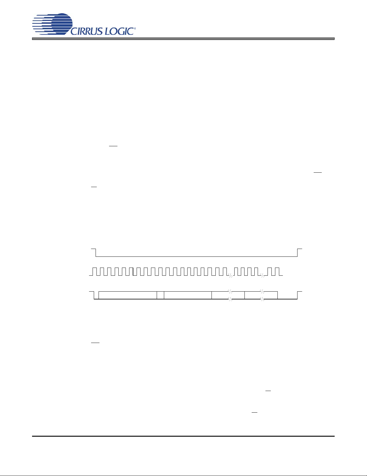
4.9 Software Mode
4 5 6 7
CCLK
CHIP ADDRESS (WRITE) MAP BYTE DATA
1 0 0 1 0 1 0 0
CDIN
INCR 6 5 4 3 2 1 0 7 6 1 0
0 1 2 3 8 9 12 16 1710 11 13 14 15
DATA +n
CS
7 6 1 0
Figure 18. Control Port Timing in SPI Mode
The control port is used to access the registers allowi ng the D/A to be configured for the desired operatio nal
modes and formats. The operation of the control port may be completely asynchronous with respect to the
audio sample rates. However, to avoid potential interference problems, the control port pins should remain
static if no operation is required.
The device enters software mode only af ter a success ful write comm and using one of two softwa re protocols: SPI or I²C, with the device acting as a slave. The SPI p rotocol is permanen tly selected whenever there
is a high-to-low transition on the AD0/CS pin after reset. If using the I²C protocol, pin AD0/CS should be
permanently connected to either VL or GND; this option allows the user to slightly alter the chip address as
desired.
4.9.1 SPI Control
In Software Mode, CS is the CS43L21 chip-select signal, CCLK is the control port bit clock (input into the
from the microcontroller), CDIN is the input data line from the microcontroller. Data is clocked in on the
rising edge of CCLK. The D/A will only support write operations. Read request will be ignored.
CS43L21
Figure 18 shows the operation of the control port in Software Mode. To write to a register, bring CS
The first seven bits on CDIN form the chip address and must be 1001010. The eighth bit is a read/write
indicator (R/W
which is set to the address of the register that is to be updated. Th e next eight bits are the data wh ich will
be placed into the register designated by the MAP.
There is MAP auto-increment capability, enabled by the INCR bit in the MAP register. If INCR is a zero,
the MAP will stay constant for successive read or writes. If INCR is set to a 1, the MAP will auto-increment
after each byte is read or written, allowing block reads or writes of successive registers.
4.9.2 I²C Control
In I²C Mode, SDA is a bidirectional data line. Data is clocked into and out of the part by the clock, SCL.
There is no CS
through a resistor to VL or DGND as desired. The state of the pin is sensed while the CS43L21 is being
reset.
low.
), which should be low to write. The next eight bits form the Memor y Address Pointer (MAP),
pin. Pin AD0 forms the least significant bit of the chip address and should be connected
The signal timings for a read and write cycle are shown in Figure 19 and Figure 20. A Start c ondition is
defined as a falling transition of SDA while the clock is high. A Stop condition is a rising transition while
the clock is high. All other transitions of SDA occur while the clock is low. The first byte sent to the
CS43L21 after a Start condition consists of a 7-bit chip address field and a R/W
bit (high for a read, low
for a write). The upper 6 bits of the 7-bit address field are fixed at 100101. To communicate with a
CS43L21, the chip address field, which is the first byte sent to the CS43L21, should match 100101 followed by the setting of the AD0 pin. The eighth bit of the address is the R/W
bit. If the operation is a write,
the next byte is the Memory Address Pointer (MAP) which selects the register to be read or written. If the
34 DS723F1
Page 35
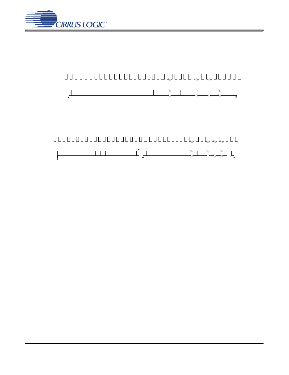
CS43L21
4 5 6 7 24 25
SCL
CHIP ADDRESS (WRITE) MAP BYTE DATA
DATA +1
START
ACK
STOP
ACKACKACK
1 0 0 1 0 1 AD0 0
SDA
INCR 6 5 4 3 2 1 0 7 6 1 0 7 6 1 0 7 6 1 0
0 1 2 3 8 9 12 16 17 18 1910 11 13 14 15 27 28
26
DATA +n
Figure 19. Control Port Timing, I²C Write
SCL
CHIP ADDRESS (WRITE)
MAP BYTE
DATA
DATA +1
START
ACK
STOP
ACK
ACK
ACK
1 0 0 1 0 1 AD0 0
SDA
1 0 0 1 0 1 AD0 1
CHIP ADDRESS (READ)
START
INCR 6 5 4 3 2 1 0
7 0 7 0 7 0
NO
168 9 12 13 14 154 5 6 7 0 1 20 21 22 23 24
26 27 28
2 3 10 11 17 18 19 25
ACK
DATA + n
STOP
Figure 20. Control Port Timing, I²C Read
operation is a read, the contents of the register pointed to by the MAP will be output. Setting the autoincrement bit in MAP allows successive reads or writes of consecutive registers. Each byte is separated
by an acknowledge bit. The ACK bit is output from the CS43L21 after each input byte is read and is in put
to the CS43L21 from the microcontroller after each transmitted byte.
Since the read operation cannot set the MAP, an aborted write operation is used as a preamble. As shown
in Figure20, the write operation is aborted after the acknowledge for the MAP byte by sending a stop condition. The following pseudocode illustrates an aborted write operation followed by a read operation.
Send start condition.
Send 100101x0 (chip address & write operation).
Receive acknowledge bit.
Send MAP byte, auto-increment off.
Receive acknowledge bit.
Send stop condition, aborting write.
Send start condition.
Send 100101x1 (chip address & read operation).
Receive acknowledge bit.
Receive byte, contents of selected register.
Send acknowledge bit.
Send stop condition.
Setting the auto-increment bit in the MAP allows successive reads or writes of consecutive registers. Each
byte is separated by an acknowledge bit.
DS723F1 35
Page 36

4.9.3 Memory Address Pointer (MAP)
The MAP byte comes after the address byte and selects the register to be read or written. Refer to the
pseudo code above for implementation details.
4.9.3.1 Map Increment (INCR)
The device has MAP auto-increment capability enabled by the INCR bit (the MSB) of the MAP. If INCR is
set to 0, MAP will stay constant for successive I²C writes or reads and SPI writes. If INCR is set to 1, MAP
will auto-increment after each byte is read or written, allowing block reads or writes of successive registers.
CS43L21
36 DS723F1
Page 37

CS43L21
5. REGISTER QUICK REFERENCE
Software mode register defaults are as shown. “Reserved” registers must maintain their default state.
AddrFunction7 6543210
01h ID Chip_ID4 Chip_ID3 Chip_ID2 Chip_ID1 Chip_ID0 Rev_ID2 Rev_ID1 Rev_ID0
p40
default
02h Power Ctl. 1 Reserved PDN_DACB PDN_DACA
p40
default
03h Speed Ctl. &
Power Ctl. 2
p41
default
04h Interface Ctl.
p42
default
05h
Reserved Reserved Reserved Reserved Reserved Reserved Reserved Reserved Reserved
default
06h
Reserved Reserved Reserved Reserved Reserved Reserved Reserved Reserved Reserved
default
07h
Reserved Reserved Reserved Reserved Reserved Reserved Reserved Reserved Reserved
11011001
Reserve Reserved Reserved Reserved
000
AUTO SPEED1 SPEED0 3-ST_SP
10101110
Reserved
00000000
00000000
10100000
M/S DAC_DIF2 DAC_DIF1 DAC_DIF0
1(See Note
2 on page
40)
1(See Note
2 on page
40)
1(See Note
2 on page
40)
1(See Note
2 on page
40)
Reserved Reserved Reserved
Reserved Reserved Reserved
PDN
0
MCLKDIV2
00000000
default
08h DAC Output
Control
p42
default
09h DAC Control DATA_SEL1 DATA_SEL0 FREEZE Reserved DEEMPH AMUTE DAC_SZC1 DAC_SZC0
p43
default
0Ah
Reserved Reserved Reserved
default
0Bh
Reserved Reserved Reserved
default
0Ch
Reserved Reserved Reserved Reserved Reserved Reserved Reserved Reserved Reserved
default
0Dh
Reserved Reserved Reserved Reserved Reserved Reserved Reserved Reserved Reserved
default
0Eh
Reserved Reserved Reserved Reserved Reserved Reserved Reserved Reserved Reserved
default
0Fh
Reserved Reserved Reserved Reserved Reserved Reserved Reserved Reserved Reserved
default
HP_GAIN2 HP_GAIN1 HP_GAIN0 DAC_SNG
VOL
01100000
00000110
Reserved
00000000
Reserved
00000000
00000000
00000000
10000000
10000000
Reserved Reserved Reserved Reserved Reserved
Reserved Reserved Reserved Reserved Reserved
INV_PCMB INV_PCMA DACB_
MUTE
DACA_
MUTE
DS723F1 37
Page 38
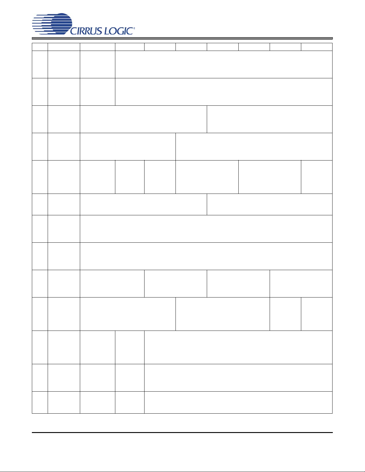
CS43L21
AddrFunction7 6543210
10h Vol. Control
PCMMIXA
p45
default
11h Vol. Control
PCMMIXB
p45
default
12h BEEP Freq. &
OnTime
p46
default
13h BEEP Off
Tim e & Vol
p46
default
14h BEEP Con-
trol & Tone
Config
p48
default
15h Tone Control TREB3 TREB2 TREB1 TREB0 BASS3 BASS2 BASS1 BASS0
p49
default
16h Vol. Control
AOUTA
p49
default
17h Vol. Control
AOUTB
p49
default
18h PCM Channel
Mixer
p50
default
19h Limiter
Threshold &
SZC Disable
p51
default
1Ah Limiter Con-
fig & Release
Rate
p52
default
1Bh Limiter Attack
Rate
p53
default
1Ch Reserved
default
MUTE_PCM
MIXA
10000000
MUTE_PCM
MIXB
10000000
FREQ3 FREQ2 FREQ1 FREQ0 ONTIME3 ONTIME2 ONTIME1 ONTIME0
00000000
OFFTIME2 OFFTIME1 OFFTIME0 BPVOL4 BPVOL3 BPVOL2 BPVOL1 BPVOL0
00000000
REPEAT BEEP Reserved TREB_CF1 TREB_CF0 BASS_CF1 BASS_CF0 TC_EN
00000000
10001000
AOUTA_
VOL7
00000000
AOUTB_
VOL7
00000000
PCMA1 PCMA0 PCMB1 PCMB0
00000000
MAX2 MAX1 MAX0 CUSH2 CUSH1 CUSH0 LIM_SRDIS LIM_ZCDIS
00000000
LIMIT_EN LIMIT_ALL LIM_R-
01111111
Reserved Reserved LIM_ARATE5 LIM_ARATE4 LIM_ARATE3 LIM_ARATE2 LIM_ARATE1 LIM_ARATE0
00000000
PCMMIXA
VOL6
PCMMIXB
VOL6
AOUTA_
VOL6
AOUTB_
VOL6
PCMMIXA
VOL5
PCMMIXB
VOL5
AOUTA_
VOL5
AOUTB_
VOL5
RATE5
PCMMIXA
VOL4
PCMMIXB
VOL4
OUTA_ VOL4 AOUTA_
AOUTB_
VOL4
PCMMIXA
VOL3
PCMMIXB
VOL3
VOL3
AOUTB_
VOL3
Reserved Reserved Reserved Reserved
LIM_R-
RATE4
LIM_RRATE3
PCMMIXA
VOL2
PCMMIXB
VOL2
AOUTA_
VOL2
AOUTB_
VOL2
LIM_RRATE2
PCMMIXA
VOL1
PCMMIXB
VOL1
AOUTA_
VOL1
AOUTB_
VOL1
LIM_RRATE1
PCMMIXA
VOL0
PCMMIXB
VOL0
AOUTA_
VOL0
AOUTB_
VOL0
LIM_RRATE0
Reserved Reserved Reserved Reserved Reserved Reserved Reserved Reserved
00000000
38 DS723F1
Page 39

CS43L21
AddrFunction7 6543210
1Dh Reserved Reserved Reserved
default
1Eh Reserved
default
1Fh Reserved
default
20h Status Reserved SP_CLK
p53
default
21h CHRG_
p54
default
00111111
Reserved Reserved Reserved Reserved Reserved Reserved
00000000
Reserved Reserved Reserved Reserved Reserved Reserved Reserved Reserved
00000000
ERR
00000000
CHRG_
FREQ3
01010000
FREQ2
Reserved Reserved Reserved Reserved Reserved Reserved
Reserved Reserved
SPEB_OVFL SPEA_OVFL PCMA_OVFL PCMB_OVFL
CHRG_
FREQ1
CHRG_
FREQ0
Reserved Reserved Reserved Reserved
Reserved Reserved
DS723F1 39
Page 40
CS43L21
6. REGISTER DESCRIPTION
All registers are read/write except for the chip I.D. and Revision Register and Interrupt Status Register which are
read only. See the following bit definition tables for bit assignment information. The default stat e of ea ch b it afte r a
power-up sequence or reset is listed in each bit description.
All “Reserved” registers must maintain their default state.
6.1 Chip I.D. and Revision Register (Address 01h) (Read Only)
76543210
Chip_ID4 Chip_ID3 Chip_ID2 Chip_ID1 Chip_ID0 Rev_ID2 Rev_ID1 Rev_ID0
Chip I.D. (Chip_ID[4:0])
Default: 11011
Function:
I.D. code for the CS43L21. Permanently set to 11011.
Chip Revision (Rev_ID[2:0])
Default: 001
Function:
CS43L21 revision level. Revision B is coded as 001. Revision A is coded as 000.
6.2 Power Control 1 (Address 02h)
76543210
Reserved PDN_DACB PDN_DACA Reserved Reserved Reserved Reserved PDN
Notes:
1. To activate the power-down sequence for individual channels (A or B,) both channels must first be powered down either by enabling the PDN bit or by enabling the power-down bits for both channels. Enabling the power-down bit on an individual channel basis after the D/A has fully powered up will mute
the selected channel without achieving any power savings.
2. Reserved bits 1 - 4 should always be set “high” by the user to minimize powe r consumption d uring normal operation.
Recommended channel power-down sequence: 1.) Enable the PDN bit, 2.) enable power-d own for the select channels, 3.) disable the PDN bit.
Power Down DAC X (PDN_DACX)
Default: 0
0 - Disable
1 - Enable
Function:
DAC channel x will either enter a power-down or muted state when this bit is enabled. See above.
Power Down (PDN)
Default: 0
0 - Disable
1 - Enable
40 DS723F1
Page 41

CS43L21
Function:
The entire D/A will enter a low-power state when this function is enabled. The contents of the control port
registers are retained in this mode.
6.3 Speed Control (Address 03h)
76543210
AUTO SPEED1 SPEED0 3-ST_SP Reserved Reserved Reserved MCLKDIV2
Auto-Detect Speed Mode (AUTO)
Default: 1
0 - Disable
1 - Enable
Function:
Enables the auto-detect circuitry for detecting the speed mo de of the D/A when oper ating as a slave. When
AUTO is enabled, the MCLK/LRCK ratio must be implemented according to Table 3 on page 29. The
SPEED[1:0] bits are ignored when this bit is enabled. Speed is determined by the MCLK/LRCK ratio.
Speed Mode (SPEED[1:0])
Default: 01
11 - Quarter-Speed Mode (QSM) - 4 to 12.5 kHz sample rates
10 - Half-Speed Mode (HSM) - 12.5 to 25 kHz sample rates
01 - Single-Speed Mode (SSM) - 4 to 50 kHz sample rates
00 - Double-Speed Mode (DSM) - 50 to 100 kHz sample rates
Function:
Sets the appropriate speed mode for the D/A in Master or Slave Mod e. QSM is optimized for 8 kHz sample
rate and HSM is optimized for 16 kHz sample rate. These bits are ignored when the AUTO bit is enabled
(see Auto-Detect Speed Mode (AUTO) above).
Tri-State Serial Port Interface (3ST_SP)
Default: 0
0 - Disable
1 - Enable
Function:
When enabled and the device is configured as a master, the SCLK/LRCK signals are placed in a high-im-
pedance output state. If the serial port is configured as a slave, SCLK/LRCK are configured as inputs.
MCLK Divide By 2 (MCLKDIV2)
Default: 0
0 - Disabled
1 - Divide by 2
Function:
Divides the input MCLK by 2 prior to all internal circuitry. This bit is ignored when the AUTO bit is disabled
in Slave Mode.
DS723F1 41
Page 42

CS43L21
6.4 Interface Control (Address 04h)
76543210
Reserved M/S
Master/Slave Mode (M/S)
Default: 0
0 - Slave
1 - Master
Function:
Selects either master or slave operation for the serial port.
DAC Digital Interface Format (DAC_DIF[2:0])
Default = 000
DAC_DIF[2:0] Description Figure
000 Left-Justified, up to 24-bit data 15 on page 31
001 I²S, up to 24-bit data 14 on page 30
010 Right-Justified, 24-bit data 16 on page 3116 on page 31
011 Right-Justified, 20-bit data 16 on page 3116 on page 31
100 Right-Justified, 18-bit data 16 on page 3116 on page 31
101 Right-Justified, 16-bit data 16 on page 3116 on page 31
110 Reserved 100 Reserved -
DAC_DIF2 DAC_DIF1 DAC_DIF0 Reserved Reserved Reserved
Function:
Selects the digital interface format used for the data in on SDIN. The required relationship between the
Left/Right clock, serial clock and serial data is defined by the Digital Interface Format and the options are
detailed in the section “Digital Interface Formats” on page 30.
6.5 DAC Output Control (Address 08h)
76543210
HP_GAIN2 HP_GAIN1 HP_GAIN0
Headphone Analog Gain (HP_GAIN[2:0])
Default: 011
HP_GAIN[2:0] Gain Setting
000 0.3959
001 0.4571
010 0.5111
011 0.6047
100 0.7099
101 0.8399
110 1.0000
111 1.1430
Function:
DAC_
SNGVOL
INV_PCMB INV_PCMA DACB_MUTE DACA_MUTE
42 DS723F1
Page 43

CS43L21
These bits select the gain multiplier for the headphone/line outputs. See “Line Output Voltage Character is-
tics” on page 14 and “Headphone Output Power Characteristics” on page 15.
DAC Single Volume Control (DAC_SNGVOL)
Default: 0
Function:
The individual channel volume levels are independently controlled by their respective Volume Control reg-
isters when this function is disabled. When enabled, the volume on all channels is determined by the AOUTA Volume Control register and the AOUTB Volume Control register is ignored.
PCMX Invert Signal Polarity (INV_PCMX)
Default: 0
0 - Disabled
1 - Enabled
Function:
When enabled, this bit will invert the signal polarity of the PCM x channel.
DACX Channel Mute (DACX_MUTE)
Default: 0
0 - Disabled
1 - Enabled
Function:
The output of channel x DAC will mute when enabled. The muting function is affected by the DACx Soft and
Zero Cross bits (DACx_SZC[1:0]).
6.6 DAC Control (Address 09h)
76543210
DATA_SEL1 DATA_SEL0 FREEZE Reserved DEEMPH AMUTE DAC_SZC1 DAC_SZC0
DAC Data Selection (DATA_SEL[1:0])
Default: 00
00 - PCM Serial Port to DAC
01 - Signal Processing Engine to DAC
10 - Reserved
11 - Reserved
Function:
Selects the digital signal source for the DAC.
Note: Certain functions are only available when the “Signal Processing Engine to DAC” option is selected
using these bits.
Freeze Controls (FREEZE)
Default: 0
Function:
DS723F1 43
Page 44

CS43L21
This function will freeze the previous settings of, and allow modifications to be made to all control port registers without the changes taking effect until the FREEZE is disabled. To have multiple chang es in the control port registers take effect simultaneously, enable the FREEZE bit, make all register changes, then
disable the FREEZE bit.
Notes:
1. This bit should only be used to synchronize run-time controls, such as volume and mute, during
normal operation. Using this bit before the relevant circuitry begins normal operation could cause the
change to take effect immediately, ignoring the FREEZE bit.
DAC De-Emphasis Control (DEEMPH)
Default: 0
0 - No De-Emphasis
1 - De-Emphasis Enabled
Function:
Note: The DATA_SEL[1:0] bits in reg09h must be set to ‘01’b to enable function control.
Enables the digital filter to apply the standard 15s/50s digital de-emphasis filter response for a sample
rate of 44.1 kHz.
Analog Output Auto MUTE (AMUTE)
Default: 0
0 - Auto Mute Disabled
1 - Auto Mute Enabled
Function:
Enables (or disables) Automatic Mute of the analog outputs after 8192 “0” samples on each digital input
channel.
DAC Soft Ramp and Zero Cross Control (DAC_SZC[1:0])
Default = 10
00 - Immediate Change
01 - Zero Cross
10 - Soft Ramp
11 - Soft Ramp on Zero Crossings
Function:
Note: The DATA_SEL[1:0] bits in reg09h must be set to ‘01’b to enable function control
Immediate Change
When Immediate Change is selected all volume-level changes will take effect immediately in one step.
Zero Cross
This setting dictates that signal-level changes, either by gain changes, attenuation changes or muting, will
occur on a signal zero crossing to minimize audible artifacts. The requested level change will occur after a
timeout period between 1024 and 2048 sample periods (21.3 ms to 42.7 ms at 48 kHz sample rate) if the
signal does not encounter a zero crossing . The zer o cross func tion is indep endently monitored and imple mented for each channel. Note: The LIM_SRDIS bit is ignored.
44 DS723F1
Page 45

Soft Ramp
Soft Ramp allows level changes, either by gain changes, attenuati on changes or muting, to be implemente d
by incrementally ramping, in 1/8 dB steps, from the current level to the new level at a rate of 0.5 dB per 4
left/right clock periods.
Soft Ramp on Zero Crossing
This setting dictates that signal-level changes, either by gain changes, attenuation changes or muting, will
occur in 1/8 dB steps and be implemented on a signal zero crossing. The 1/8 dB level change will occur
after a timeout period between 512 and 1024 sample periods (10.7 ms to 21.3 ms at 48 kHz sample rate) if
the signal does not encounter a zero crossing. The zero cross fu nctio n is indepe nde ntly mon ito red an d implemented for each channel. Note: The LIM_SRDIS bit is ignored.
6.7 PCMX Mixer Volume Control: PCMA (Address 10h) & PCMB (Address 11h)
76543210
MUTE_
PCMMIXx
Note: The DATA_SEL[1:0] bits in reg09h must be set to ‘01’b to enable function control in this register.
PCMX Mixer Channel Mute (MUTE_PCMMIXX)
PCMMIXx_
VOL6
PCMMIXx_
VOL5
PCMMIXx_
VOL4
PCMMIXx_
VOL3
PCMMIXx_
VOL2
PCMMIXx_
VOL1
CS43L21
PCMMIXx_
VOL0
Default = 1
0 - Disabled
1 - Enabled
Function:
The PCM channel X input to the output mixer will mute when enabled. The muting function is affected by
the DACX Soft and Zero Cross bits (DACX_SZC[1:0]).
PCMX Mixer Volume Control (PCMMIXX_VOL[6:0])
Default: 000 0000
Binary Code Volume Setting
001 1000 +12.0 dB
··· ···
000 0000 0 dB
111 1111 -0.5 dB
111 1110 -1.0 dB
··· ···
001 1001 -51.5 dB
Function:
The level of the PCMX input to the output mixer can be adjusted in 0.5 dB increments as dictated by the
DACX Soft and Zero Cross bits (DACX_SZC[1:0]) from +12 to -51.5 dB. Levels are decoded as described
in the table above.
DS723F1 45
Page 46

CS43L21
6.8 Beep Frequency & Timing Configuration (Address 12h)
76543210
FREQ3 FREQ2 FREQ1 FREQ0 ONTIME3 ONTIME2 ONTIME1 ONTIME0
Note: The DATA_SEL[1:0] bits in reg09h must be set to ‘01’b to enable function control in this register.
Beep Frequency (FREQ[3:0])
Default: 0000
FREQ[3:0] Frequency
Pitch
Fs = 12, 24, 48 or 96
kHz
0000 260.87 Hz C4
0001 521.74 Hz C5
0010 585.37 Hz D5
0011 666.67 Hz E5
0100 705.88 Hz F5
0101 774.19 Hz G5
0110 888.89 Hz A5
0111 1000.00 Hz B5
1000 1043.48 Hz C6
1001 1200.00 Hz D6
1010 1333.33 Hz E6
1011 1411.76 Hz F6
1100 1600.00 Hz G6
1101 1714.29 Hz A6
1110 2000.00 Hz B6
1111 2181.82 Hz C7
Function:
The frequency of the beep signal can be adjusted from 260.87 Hz to 2181.82 Hz. Beep frequency will scale
directly with sample rate, Fs, but is fixe d at th e no m ina l F s wit hin e ac h s peed m o de . R efe r to Figure 10 on
page 26 for single, multiple and continuous beep configurations using the REPEAT and BEEP bits.
Beep On Time Duration (ONTIME[3:0])
Default: 0000
TIME[3:0]
0000 86 ms
··· ···
1111 5.2 s
Fs = 12, 24, 48 or 96 kHz
On Time
Function:
The on-duration of the beep signal can be adjusted from approximate ly 86 ms to 5.2 s. The on-duration will
scale inversely with sample rate, Fs, but is fixed at the nominal Fs within each speed mode. Refer to Figure
10 on page 26 for single-, multiple- and continuous-beep configurations using the REPEAT and BEEP bits.
6.9 Beep Off Time & Volume (Address 13h)
76543210
OFFTIME2 OFFTIME1 OFFTIME0 BPVOL4 BPVOL3 BPVOL2 BPVOL1 BPVOL0
46 DS723F1
Page 47

Note: The DATA_SEL[1:0] bits in reg09h must be set to ‘01’b to enable function control in this register.
Beep Off Time (OFFTIME[2:0])
Default: 000
OFFTIME[2:0] Off Time
Fs = 12, 24, 48 or
96 kHz
000 1.23 s
001 2.58 s
010 3.90 s
011 5.20 s
100 6.60 s
101 8.05 s
110 9.35 s
111 10.80 s
Function:
The off-duration of the beep signal can be adjus ted from approximately 75 ms to 680 ms. The off-duration
will scale inversely with sample rate, Fs, but is fixed at the nominal Fs within each speed mode. Refer to
Figure 10 on page 26 for single-, multiple- and continuous-beep configurations using the REPEAT and
BEEP bits.
CS43L21
Beep Volume (BPVOL[4:0])
Default: 00000
Binary Code Volume Setting
00110 +12 .0 dB
··· ···
00000 0 dB
11111 -2 dB
11110 -4 dB
··· ···
00111 -50 dB
Function:
The level of the beep into the output mixer can be adjusted in 2.0 dB increments from +12 dB to -50 dB.
Refer to Figure 10 on page 26 for single-, multiple- and continuous-beep configurations using the REPEAT
and BEEP bits. Levels are decoded as described in the table above.
DS723F1 47
Page 48

CS43L21
6.10 Beep Configuration & Tone Configuration (Address 14h)
76543210
REPEAT BEEP Reserved TREB_CF1 TREB_CF0 BASS_CF1 BASS_CF0 TC_EN
Note: The DATA_SEL[1:0] bits in reg09h must be set to ‘01’b to enable function control in this register.
Repeat Beep (REPEAT)
Default: 0
0 - Disabled
1 - Enabled
Function:
This bit is used in conjunction with the BEEP bit to mix a continuous or periodic beep with the analog output.
Refer to Figure 10 on page 26 for a description of each configuration option.
Beep (BEEP)
Default: 0
0 - Disabled
1 - Enabled
Function:
This bit is used in conjunction with the REPEAT bit to mix a continuous or periodic beep with the analog
output. Note: Re-engaging the beep be fore it has completed its initial cycle will cause the beep signal to
remain ON for the maximum ONTIME duration. Refer to Figure 10 on page 26 fo r a description of each configuration option.
Treble Corner Frequency (TREB_CF[1:0])
Default: 00
00 - 5 kHz
01 - 7 kHz
10 - 10 kHz
11 - 15 kHz
Function:
The treble corner frequency is user selectable as shown above.
Bass Corner Frequency (BASS_CF[1:0])
Default: 00
00 - 50 Hz
01 - 100 Hz
10 - 200 Hz
11 - 250 Hz
Function:
The bass corner frequency is user-selectable as shown above.
48 DS723F1
Page 49
CS43L21
Tone Control Enable (TC_EN)
Default = 0
0 - Disabled
1 - Enabled
Function:
The Bass and Treble tone control features are active when this bit is enabled.
6.11 Tone Control (Address 15h)
76543210
TREB3 TREB2 TREB1 TREB0 BASS3 BASS2 BASS1 BASS0
Note: The DATA_SEL[1:0] bits in reg09h must be set to ‘01’b to enable function control in this register.
Treble Gain Level (TREB[3:0])
Default: 1000 dB (No Treble Gain)
Binary Code Gain Setting
0000 +12.0 dB
··· ···
01 11 +1.5 dB
1000 0 dB
1001 -1.5 dB
··· ···
1111 -10.5 dB
Function:
The level of the shelving treble gain filter is set by Treble Gain Level. The level can be adjusted in 1.5 dB
increments from +12.0 to -10.5 dB.
Bass Gain Level (BASS[3:0])
Default: 1000 dB (No Bass Gain)
Binary Code Gain Setting
0000 +12.0 dB
··· ···
01 11 +1.5 dB
1000 0 dB
1001 -1.5 dB
··· ···
1111 -10.5 dB
Function:
The level of the shelving ba ss ga in filte r is s et by Bass Gain Level. The level can be adjusted in 1.5 dB in-
crements from +10.5 to -10.5 dB.
6.12 AOUTx Volume Control:
DS723F1 49
Page 50
CS43L21
LR+
2
------------
LR+
2
------------
AOUTA (Address 16h) & AOUTB (Address 17h)
76543210
AOUTx_VOL7 AOUTx_VOL6 AOUTx_VOL5 AOUTx_VOL4 AOUTx_VOL3 AOUTx_VOL2 AOUTx_VOL1 AOUTx_VOL0
Note: The DATA_SEL[1:0] bits in reg09h must be set to ‘01’b to enable function control in this register.
AOUTX Volume Control (AOUTX_VOL[7:0])
Default = 00h
Binary Code Volume Setting
0001 1000 +12.0 dB
··· ···
0000 0000 0 dB
1111 1111 -0.5 dB
1111 1110 -1.0 dB
··· ···
0011 0100 -102 dB
··· ···
0001 1001 -102 dB
Function:
The analog output levels can be adjusted in 0.5 dB increments from +12 to - 102 dB as dictated by the DAC
Soft and Zero Cross bits (DACX_SZC[1:0]). Levels are decoded in unsigned binary as described in the table
above.
Note: When the limiter is enabled, the AOUT Volume is automatically controlled and should not be ad-
justed manually. Alternative volume control may be achieved using the PCMMIXx_VOL[6:0] bits.
6.13 PCM Channel Mixer (Address 18h)
76543210
PCMA1 PCMA0 PCMB1 PCMB0 Reserved Reserved Reserved Reserved
Note: The DATA_SEL[1:0] bits in reg09h must be set to ‘01’b to enable function control in this register.
Channel Mixer (PCMx[1:0] )
Default: 00
PCMA[1:0] AOUTA PCMB[1:0] AOUTB
00 L 00 R
01 01
10 10
11 R 11 L
Function:
Implements mono mixes of the left and right channels as well as a left/right channel swap.
50 DS723F1
Page 51
CS43L21
6.14 Limiter Threshold SZC Disable (Address 19h)
76543210
MAX2 MAX1 MAX0 CUSH2 CUSH1 CUSH0 LIM_SRDIS LIM_ZCDIS
Note: The DATA_SEL[1:0] bits in reg09h must be set to ‘01’b to enable function control in this register.
Maximum Threshold (MAX[2:0])
Default: 000
MAX[2:0] Threshold
Setting
(dB)
000 0
001 -3
010 -6
011 -9
101 -12
101 -18
110 -24
111 -30
Function:
Sets the maximum level, below full scale, at which to limit and attenuate the output signal at the attack rate.
Bass, Treble and digital gain settings that boost the signal beyond the maximum threshold may trigger an
attack.
Cushion Threshold (CUSH[2:0])
Default: 000
CUSH[2:0] Threshold
Setting
(dB)
000 0
001 -3
010 -6
011 -9
101 -12
101 -18
110 -24
111 -30
Function:
Sets a cushion level below full scale. This setting is usually set slightly below the maximum (MAX[2:0])
threshold. The Limiter uses this cushion as a hysteresis point for the input signal as it maintains the signal
below the maximum as well as below the cushion setting. This provides a more natural sound as the limiter
attacks and releases.
DS723F1 51
Page 52

CS43L21
Limiter Soft Ramp Disable (LIM_SRDIS)
Default: 0
0 - Off
1 - On
Function:
Overrides the DAC_SZC setting. When this bit is set, the Limiter attack and release rate will not be dictated
by the soft ramp setting. Note: This bit is ignored when the zero-cross function is enabled (i.e. when
DAC_SZC[1:0] = ‘01’b or ‘11’b.)
Limiter Zero Cross Disable (LIM_ZCDIS)
Default: 0
0 - Off
1 - On
Function:
Overrides the DAC_SZC setting. When this bit is set, the Limiter attack and release rate will not be dictated
by the zero-cross setting.
6.15 Limiter Release Rate Register (Address 1Ah)
76543210
LIMIT_EN LIMIT_ALL RRATE5 RRATE4 RRATE3 RRATE2 RRATE1 RRATE0
Note: The DATA_SEL[1:0] bits in reg09h must be set to ‘01’b to enable function control in this register.
Peak Detect and Limiter Enable (LIMIT_EN)
Default: 0
0 - Disabled
1 - Enabled
Function:
Limits the maximum signal amplitude to prevent cli pping when this function is enabled. Peak Signal Limiting
is performed by digital attenuation. Note: When the limiter is enabled, the AOUT Volume is automatically
controlled and should not be adjusted manually. Alternative volume control may be realized using the PCMMIXx_VOL[6:0] bits.
Peak Signal Limit All Channels (LIMIT_ALL)
Default: 1
0 - Individual Channel
1 - Both channels A & B
Function:
When set to 0, the peak signal limiter will limit the maximum signal amplitude to prevent clipping on the spe-
cific channel indicating clipping. The other channels will not be affected.
When set to 1, the peak signal limiter will limit the maximum signal amplitude to prevent clipping on both
channels in response to any single channel indicating clipping.
52 DS723F1
Page 53

Limiter RELEASE Rate (RRATE[5:0])
CS43L21
Default: 111111
Binary Code Release Time
000000 Fastest Release
111111 Slowest Release
Function:
Sets the rate at which the limiter releases the digital attenuation from levels below the minimum setting in
the limiter threshold register, and returns the analog output level to the AOUTx_VOL[7:0] setting.
The limiter release rate is user selectable but is also a function of the sampling frequency, Fs, and the
DAC_SZC setting unless the disable bit is enabled.
··· ···
6.16 Limiter Attack Rate Register (Address 1Bh)
76543210
Reserved Reserved ARATE5 ARATE4 ARATE3 ARATE2 ARATE1 ARATE0
Note: The DATA_SEL[1:0] bits in reg09h must be set to ‘01’b to enable function control in this register.
Limiter Attack Rate (ARATE[5:0])
Default: 000000
Binary Code Attack Time
000000 Fastest Attack
··· ···
111111 Slowest Attack
Function:
Sets the rate at which the limiter attenuates the analog ou tput from levels above the maximum setting in th e
limiter threshold register.
The limiter attack rate is user-selectable but is also a function of the sampling frequency, Fs, and the
DAC_SZC setting unless the disable bit is enabled.
6.17 Status (Address 20h) (Read Only)
76543210
Reserved SP_CLKERR SPEA_OVFL SPEB_OVFL PCMA_OVFL PCMB_OVFL Reserved Reserved
For all bits in this register, a “1” means the associated error condition has occurred at least once since the
register was last read. A ”0” means the associated error condition has NOT occurred since the last reading
of the register. Reading the register resets all bits to 0.
Serial Port Clock Error (SP_CLK Error)
Default: 0
Function:
Indicates an invalid MCLK to LRCK ratio. See “Serial Port Clocking” section on page 28“Serial Port Clock-
ing” on page 28 for valid clock ratios.
Note: On initial power up and application of clocks, this bit will be high as the serial port re-synchronizes.
DS723F1 53
Page 54

CS43L21
64xFs
N2+
---------------- -
Signal Processing Engine Overflow (SPEX_OVFL)
Default: 0
Function:
Indicates a digital overflow condition within the data path after the signal processing engine.
PCMX Overflow (PCMX_OVFL)
Default: 0
Function:
Indicates a digital overflow condition within the data pat h of th e PCM mi x.
6.18 Charge Pump Frequency (Address 21h)
76543210
CHRG_-
FREQ3
Charge Pump Frequency (CHRG_FREQ[3:0])
Default: 0101
N CHRG_FREQ[3:0] Frequency
... ...
15 1111
CHRG_-
FREQ2
0 0000
CHRG_-
FREQ1
CHRG_-
FREQ0
Reserved Reserved Reserved Reserved
Function:
Alters the clocking frequency of the charge pump in 1/(N+2) fractions of the DAC o versampling rate, 128 Fs,
should the switching frequency interfere with other system frequencies such as those in the AM radio band.
Note: Distortion performance may be affected.
54 DS723F1
Page 55
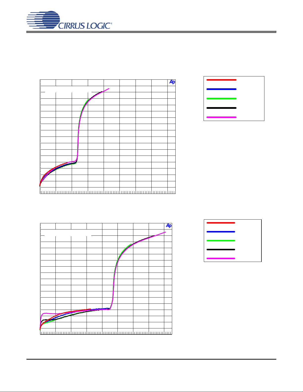
7. ANALOG PERFORMANCE PLOTS
G = 0.6047
G = 0.7099
G = 0.8399
G = 1.0000
G = 1.1430
Legend
-100
-10
-95
-90
-85
-80
-75
-70
-65
-60
-55
-50
-45
-40
-35
-30
-25
-20
-15
d
B
r
A
0 80m10m 20m 30m 40m 50m 60m 70m
W
Figure 21. THD+N vs. Output Power per Channel at 1.8 V (16 load)
VA_HP = VA = 1.8 V
NOTE: Graph shows the output power per channel (i.e.
Output Power = 23 mW into
single 16 and 46 mW into
stereo 16 with THD+N = 75 dB).
G = 0.6047
G = 0.7099
G = 0.8399
G = 1.0000
G = 1.1430
Legend
-100
-10
-95
-90
-85
-80
-75
-70
-65
-60
-55
-50
-45
-40
-35
-30
-25
-20
-15
d
B
r
A
0 80m10m 20m 30m 40m 50m 60m 70m
W
Figure 22. THD+N vs. Output Power per Channel at 2.5 V (16 load)
VA_HP = VA = 2.5 V
NOTE: Graph shows the output power per channel (i.e.
Output Power = 44 mW into
single 16 and 88 mW into
stereo 16 with THD+N = 75 dB).
7.1 Headphone THD+N versus Output Power Plots
Test conditions (unless otherwise spec ified): Input test signal is a 99 7 Hz sine wave; measurement bandwidth is 10 Hz to 20 kHz; Fs = 48 kHz. Plots were taken from the CDB43L21 using an Audio Precision analyzer.
CS43L21
DS723F1 55
Page 56
G = 0.6047
G = 0.7099
G = 0.8399
G = 1.0000
G = 1.1430
Legend
-100
-20
-95
-90
-85
-80
-75
-70
-65
-60
-55
-50
-45
-40
-35
-30
d
B
r
A
0 60m6m 12m 18m 24m 30m 36m 42m 48m 54m
W
Figure 23. THD+N vs. Output Power per Channel at 1.8 V (32 load)
VA_HP = VA = 1.8
NOTE: Graph shows the output power per channel (i.e.
Output Power = 22 mW into
single 32 and 44 mW into
stereo 32 with THD+N = 75 dB).
G = 0.6047
G = 0.7099
G = 0.8399
G = 1.0000
G = 1.1430
Legend
-100
-20
-95
-90
-85
-80
-75
-70
-65
-60
-55
-50
-45
-40
-35
-30
-25
d
B
r
A
0 60m5m 10m 15m 20m 25m 30m 35m 40m 45m 50m 55m
W
Figure 24. THD+N vs. Output Power per Channel at 2.5 V (32 load)
VA_HP = VA = 2.5 V
NOTE: Graph shows the output power per channel (i.e.
Output Power = 42 mW into
single 32 and 84 mW into
stereo 32 with THD+N = 75 dB).
CS43L21
56 DS723F1
Page 57

7.2 Headphone Amplifier Efficiency
Figure 25. Power Dissipation vs. Output Power into Stereo 16
VA_HP = VA = 1.8 V
Figure 26. Power Dissipation vs. Output Power into Stereo 16 (Log Detail)
VA_HP = VA = 1.8 V
The architecture of the headphone amplifier is that of typical class AB amplifiers. Test conditions (unless
otherwise specified): Input test signal is a 997 Hz sine wave; Power Consumption Mode 6 - Stereo Playback
with 16- load. HP_GAIN = 1.1430. Best efficiency is realized when the amplifier outputs maximum power.
CS43L21
DS723F1 57
Page 58

8. EXAMPLE SYSTEM CLOCK FREQUENCIES
8.1 Auto Detect Enabled
CS43L21
Sample Rate
LRCK (kHz)
8 8.1920 12.2880 16.3840 24.5760
11.025 11.2896 16.9344 22.5792 33.8688
12 12.2880 18.4320 24.5760 36.8640
1024x 1536x 2048x* 3072x*
Sample Rate
LRCK (kHz)
16 8.1920 12.2880 16.3840 24.5760
22.05 11.2896 16.9344 22.5792 33.8688
24 12.2880 18.4320 24.5760 36.8640
512x 768x 1024x* 1536x*
Sample Rate
LRCK (kHz)
32 8.1920 12.2880 16.3840 24.5760
44.1 11.2896 16.9344 22.5792 33.8688
48 12.2880 18.4320 24.5760 36.8640
256x 384x 512x* 768x*
Sample Rate
LRCK (kHz)
64 8.1920 12.2880 16.3840 24.5760
88.2 11.2896 16.9344 22.5792 33.8688
96 12.2880 18.4320 24.5760 36.8640
128x 192x 256x* 384x*
MCLK (MHz)
MCLK (MHz)
MCLK (MHz)
MCLK (MHz)
*The”MCLKDIV2” pin 4 must be set HI.
58 DS723F1
Page 59
8.2 Auto Detect Disabled
CS43L21
Sample Rate
LRCK (kHz)
8 - 6.1440 8.1920 12.2880 16.3840 24.5760
11.025 - 8.4672 11.2896 16.9344 22.5792 33.8688
12 6.1440 9.2160 12.2880 18.4320 24.5760 36.8640
512x 768x 1024x 1536x 2048x 3072x
Sample Rate
LRCK (kHz)
16 - 6.1440 8.1920 12.2880 16.3840 24.5760
22.05 - 8.4672 11.2896 16.9344 22.5792 33.8688
24 6.1440 9.2160 12.2880 18.4320 24.5760 36.8640
256x 384x 512x 768x 1024x 1536x
Sample Rate
LRCK (kHz)
32 8.1920 12.2880 16.3840 24.5760
44.1 11.2896 16.9344 22.5792 33.8688
48 12.2880 18.4320 24.5760 36.8640
256x 384x 512x 768x
Sample Rate
LRCK (kHz)
64 8.1920 12.2880 16.3840 24.5760
88.2 11.2896 16.9344 22.5792 33.8688
96 12.2880 18.4320 24.5760 36.8640
128x 192x 256x 384x
MCLK (MHz)
MCLK (MHz)
MCLK (MHz)
MCLK (MHz)
DS723F1 59
Page 60

9. PCB LAYOUT CONSIDERATIONS
9.1 Power Supply, Grounding
As with any high-resolution converter, the CS43L21 requires careful attention to powe r supply and gro unding arrangements if its potential performance is to be realized. Figure 1 on pag e 9 shows the recommended
power arrangements, with VA and VA_HP connected to clean supplies. VD, which powers the digital circuitry, may be run from the system logic supply. Alternatively, VD may be powered from the analog supply via
a ferrite bead. In this case, no additional devices should be powered from VD.
Extensive use of power and ground planes, ground plane fill in unused areas and surface mount decoupling
capacitors are recommended. Decoupling capacitors should be as close to the pins of the CS43L21 as possible. The low value ceramic capacitor should be closest to the pin and should be mounted on the same
side of the board as the CS43L21 to minimize inductance effects. All signals, especially clocks, should be
kept away from the FILT+ and VQ pins in order to avoid unwanted coupling into the modulators. The FILT+
and VQ decoupling capacitors, particularly the 0.1 µF, must be positioned to minimize the electrical path
from FILT+ and AGND. The CS43L21 evaluation board demonstrates the optimum layout and power supply
arrangements.
9.2 QFN Thermal Pad
The CS43L21 is available in a compact QFN package. The under side of the QFN package reveals a large
metal pad that serves as a thermal relief to provide for maxim um heat dissipatio n. This pad must mate with
an equally dimensioned copper pad on the PCB and must be electrically connected to ground. A series of
vias should be used to connect this copper pad to one or more larger ground planes on other PCB layers.
In split ground systems, it is recommended that this thermal pad be connected to AGND for best performance. The CS43L21 evaluation board demonstrates the optimum thermal pad and via configuration.
CS43L21
60 DS723F1
Page 61

10.DIGITAL FILTERS
Figure 27. Passband Ripple Figure 28. Stopband
Figure 29. Transition Band Figure 30. Transition Band (Detail)
CS43L21
DS723F1 61
Page 62

11.PARAMETER DEFINITIONS
Dynamic Range
The ratio of the rms value of the signal t o the rms su m of all other spectral components over the specified
bandwidth. Dynamic Range is a signal-to-noise ra tio measurement over the specified b and width made with
a -60 dBFS signal. 60 dB is added to resulting measurement to refer the measurement to full-scale. This
technique ensures that the distortion components are below the noise level and do not affect the measurement. This measurement technique has been accepted by the Audio Engineering Society, AES17-1991,
and the Electronic Industries Association of Japan, EIAJ CP-307. Expressed in decibels.
Total Harmonic Distortion + Noise
The ratio of the rms value of the signal t o the rms su m of all other spectral components over the specified
band width (typically 10 Hz to 20 kHz), including distortion components. Expressed in decibels. Measured
at -1 and -20 dBFS as suggested in AES17-1991 Annex A.
Frequency Response
A measure of the amplitude r es po ns e va riatio n from 10 Hz to 20 kHz relative to the amplitude res pons e at
1 kHz. Units in decibels.
Interchannel Isolation
A measure of crosstalk between the left and right channel pairs. Measured for each channel at the converter's output with no signal to the input under test and a full-scale signal applied to the other channel. Units in
decibels.
CS43L21
Interchannel Gain Mismatch
The gain difference between left and right channel pairs. Units in decibels.
Gain Error
The deviation from the nominal full-scale analog output for a full-scale digital input.
Gain Drift
The change in gain value with temperature. Units in ppm/°C.
Offset Error
The deviation of the midscale transition (111...111 to 000...000) from the ideal. Units in mV.
12.REFERENCES
1. Philips Semiconductor, The I²C-Bus Specification: Version 2.1, January 2000.
http://www.semiconductors.philips.com
62 DS723F1
Page 63

13.PACKAGE DIMENSIONS
Side View
A1
Bottom View
Top View
A
Pin #1 Corner
D
E
D2
L
b
e Pin #1 Corner
E2
32L QFN (5 X 5 mm BODY) PACKAGE DRAWING
CS43L21
INCHES MILLIMETERS NOTE
DIM MIN NOM MAX MIN NOM MAX
A-- --0.0394-- --1.001
A1 0.0000 -- 0.0020 0.00 -- 0.05 1
b 0.0071 0.0091 0.0110 0.18 0.23 0.28 1,2
D 0.1969 BSC 5.00 BSC 1
D2 0.1280 0.1299 0.1319 3.25 3.30 3.35 1
E 0.1969 BSC 5.00 BSC 1
E2 0.1280 0.1299 0.1319 3.25 3.30 3.35 1
e 0.0197 BSC 0.50 BSC 1
L 0.0118 0.0157 0.0197 0.30 0.40 0.50 1
JEDEC #: MO-220
Controlling Dimension is Millimeters.
1. Dimensioning and tolerance per ASME Y 14.5M-1995.
2. Dimensioning lead width applies to the plated terminal and is measured between 0.20 mm and 0.25 mm
from the terminal tip.
THERMAL CHARACTERISTICS
Junction to Ambient Thermal Impedance 2 Layer Board
Parameter Symbol Min Typ Max Units
4 Layer Board
JA
-
-
52
38
-
-
°C/Watt
DS723F1 63
Page 64
CS43L21
Contacting Cirrus Logic Support
For all product questions and inquiries, contact a Cirrus Logic Sales Representative.
To find one nearest you, go to www.cirrus.com.
Cirrus Logic, Inc. and its subsidiaries ("Cirrus") believe that the information contained in this document is accurate and reliable. However, the i nformation is subj ect
to change without not ice and is provi ded "AS I S" witho ut warran ty of any k ind (ex press or implie d). Custo mers ar e advised to obtain the latest version of relevant
information to verify, before placing orders, that information being relied on is current and complete. All products are sold subject to the terms and conditions of sale
supplied at the time of order acknowled gment, includin g those pertaining to wa rranty, indemnificatio n, and limitation of liability. No responsibility is assumed by Cirrus
for the use of this information, including use of this information as the basis for manufacture or sale of any items, or for infringement of patents or other rights of third
parties. This document is the property of Cirrus and by furnishing this information, Cirrus grants no license, express or implied under any patents, mask work rights,
copyrights, trademarks, trade secrets or other intellectual property rights. Cirrus owns the copyrights associated with the information contained herein and g ives consent for copies to be made of the information only for use within your organization with respect to Cirrus integrated circuits or other products of Cirrus. This consent
does not extend to other copying such as copying for general distribution, advertising or promotional purposes, or for creating any work for resale.
CERTAIN APPLICATIONS USING SEMICONDUCTOR PRODUCTS MAY INVOLVE POTENTIAL RISKS OF DEATH, PERSONAL INJURY, OR SEVERE PROPERTY OR ENVIRONMENTAL DAMAGE (“CRITICAL APPLICATIONS”). CIRRUS PRODUCTS ARE NOT DESIGNED, AUTHORIZED OR WARRANTED FOR USE
IN AIRCRAFT SYSTEMS, MILITARY APPL ICATIONS, PRODUCTS SURGICALLY IMPL ANTED INTO THE BODY, AUTOMOT IVE SAFETY OR SECURIT Y DEVICES, LIFE SUPPORT PRODUCTS OR OTHER CRITI CAL APPLICATIONS. INCLUSION OF CIRRUS PRODUCTS IN SUCH APPLICATIONS IS UNDERSTOOD TO BE FULLY AT THE CUSTOMER’S RISK AND CIRRUS DISCLAIMS AND MAKES NO WARRANTY, EXPRESS, STATUTORY OR IMPLIED,
INCLUDING THE IMPLIED WARRANTIES OF MERCHANTABILITY AND FITNESS FOR PARTICULAR PURPOSE, WITH REGARD TO ANY CIRRUS PRODUCT
THAT IS USED IN SUCH A MANNER. IF THE CUSTOMER OR CUSTOMER’S CU STOMER USES O R PERMITS THE USE OF CIRRUS PRODUCTS IN CRITICAL
APPLICATIONS, CUSTOMER AGREES, BY SUCH USE, TO FULLY INDEMNIFY CIRRUS, ITS OFFICERS, DI RECT ORS, EMPLOYE ES, DI ST RIBUTO RS AND
OTHER AGENTS FROM ANY AND ALL LIABI LITY, INCLUDING AT TORNEYS’ FEES AN D COSTS, THAT MAY RESULT FROM OR ARISE IN CONNECTI ON
WITH THESE USES.
Cirrus Logic, Cirrus, and the Cirrus Logic logo designs are trademarks of Cirrus Logic, Inc. All other brand and product names in this document may be trademarks
or service marks of their respective owners.
I²C is a trademark of Philips Semiconductor.
SPI is a trademark of Motorola, Inc.
14.ORDERING INFORMATION
Product Description Package Pb-Free Grade Temp Range Container Order #
Rail CS43L21-CNZ
Tape & Reel CS43L21-CNZR
Rail CS43L21-DNZ
Tape & Reel CS43L21-DNZR
CS43L21
CDB43L21
Low-Power Stereo D/A
with HP Amp for Portable
Apps
CS43L21 Evaluation
Board
Commercial -10 to +70° C
32L-QFN Yes
Automotive -40 to +85° C
- No - - - CDB43L21
15.REVISION HISTORY
Revision Changes
Updated voltage range in “Specified Operating Conditions” on page 11.
Added and updated absolute maximum parameters in “Absolute Maximum Ratings” on page 11.
Updated Figure 8. Output Architecture on page 24.
F1
Updated Section 4.7 “Recommended Power-Up Sequence” on page 31.
Updated Section 4.8 “Recommended Power-Down Sequence” on page 32.
Updated Section 4.9 “Software Mode” on page 34 .
Added note 1in the FREEZE control register in “DAC Control (Address 09h)” on page 43.
64 DS723F1
 Loading...