

Page 1
CS4392
24-Bit, 192 kHz Stereo DAC with Volume Control
Features
z Complete Stereo DAC System: Interpolation,
D/A, Output Analog Filtering
z 114 dB Dynamic Range
z 100 dB THD+N
z Up to 192kHz Sample Rates
z Direct Stream Digital Mode
z Low Clock Jitter Sensitivity
z Single +5 V Power Supply
z Selectable Digital Filters
– Fast and Slow roll-off
z Volume Control with Soft Ramp
– 1 dB Step Size
– Zero Crossing Click-Free Transitions
z Direct Interface with 5 V to 1.8 V Logic
z ATAPI Mixing Functions
z Pin Compatible with the CS4391
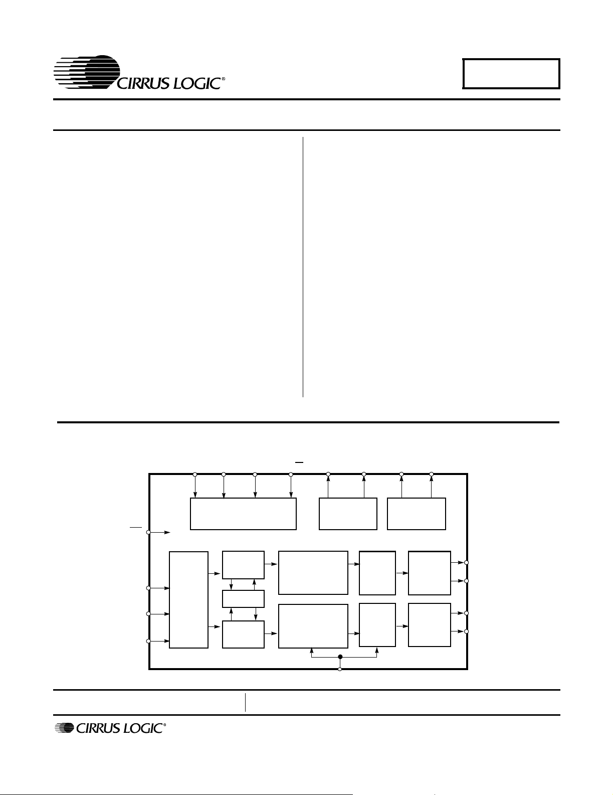
I
Description
The CS4392 is a complete stereo digital-to-analog system including digital interpolation, fifth-order delta-sigma
digital-to-analog conversion, digital de-emphasis, volume control, channel mixing and analog filtering. The
advantages of this architecture include: ideal differential
linearity, no distortion mechanisms due to resistor
matching errors, no linearity drift over time and temperature, and a high tolerance to clock jitter.
The CS4392 accepts PCM data at sample rates from
4 kHz to 192 kHz, DSD audio data, has selectable digital
filters, and consumes very little power. These features
are ideal for DVD, SACD players, A/V receivers, CD and
set-top box systems. The CS4392 is pin and register
compatible with the CS4391, making easy performance
upgrades possible.
ORDERING INFORMATION
CS4392-KS -10 to 70 °C 20-pin SOIC
C S 4 3 9 2 - K Z - 1 0 t o 7 0 ° C 2 0 - p i n T S S O P
C S 4 3 9 2 - K Z Z , L e a d F r e e - 1 0 t o 7 0 ° C 2 0 - p i n T S S O P
CDB4392 Evaluation Board
M1
RST
SCLK
LRCK
SDATA
(SDA/CDIN)
SERIAL
PORT
M3
MODE SELECT
(CONTROL PORT)
Preliminary Product Information
http://www.cirrus.com
M2
(SCL/CCLK) (AD0/CS)
VOLUME
CONTROL
MIXER
VOLUME
CONTROL
M0
AMUTEC
MUTE CONTROL
INTERPOLATION
FILTER
INTERPOLATION
FILTER
EXTERNAL
MCLK
∆Σ
DAC
∆Σ
DAC
CMOUT
REFERENCE
FILT+BMUTEC
ANALOG
FILTER
ANALOG
FILTER
This document contains information for a new product.
Cirrus Logic reserves the right to modify this product without notice.
Copyright © Cirrus Logic, Inc. 2002
(All Rights Reserved)
AOUTA+
AOUTA-
AOUTB+
AOUTB-
SEP ‘04
DS459PP3
Page 2

TABLE OF CONTENTS
1. PIN DESCRIPTION - PCM DATA MODE .................................................................... 5
1.1 PIN DESCRIPTION - DSD mode ..................................................................... 6
2. TYPICAL CONNECTION DIAGRAMS ........................................................................ 7
3. APPLICATIONS ........................................................................................................... 9
3.1 Recommended Power-up Sequence for Hardware Mode ................................ 9
3.2 Recommended Power-up Sequence and Access to
Control Port Mode ............................................................................................. 9
3.3 Analog Output and Filtering .............................................................................. 9
3.4 Interpolation Filter ........................................................................................... 10
3.5 System Clocking ............................................................................................. 10
3.6 Digital Interface Format .................................................................................. 11
3.7 De-Emphasis .................................................................................................. 12
3.8 Oversampling Modes ...................................................................................... 12
3.9 Using DSD mode ............................................................................................ 13
3.10 Mute Control ................................................................................................. 13
4. CONTROL PORT INTERFACE ................................................................................. 14
4.0.1 MAP Auto Increment ............................................................................. 14
4.0.2 I2C Mode ............................................................................................... 14
4.0.3 SPI Mode ............................................................................................... 16
4.1 Memory Address Pointer (MAP) ...................................................................... 16
5. REGISTER QUICK REFERENCE ............................................................................. 17
6. REGISTER DESCRIPTION ........................................................................................ 18
6.1 Mode Control 1 - Address 01h ........................................................................ 18
6.1.1 Auto-Mute (Bit 7) ................................................................................... 18
6.1.2 Digital Interface Formats (Bits 6:4) ........................................................ 18
6.1.3 De-Emphasis Control (Bits 3:2) ............................................................. 19
6.1.4 Functional Mode (Bits 1:0) .................................................................... 19
6.2 Volume and Mixing Control (Address 02h) ..................................................... 20
6.2.1 Channel A Volume = Channel B Volume (Bit 7) .................................... 20
CS4392
I2C Write.................................................................................................... 14
I2C Read ................................................................................................... 15
SPI Write.................................................................................................... 16
Contacting Cirrus Logic Support
For all product questions and inquiries contact a Cirrus Logic Sales Representative.
To find one nearest you go to http://www.cirrus.com/corporate/contacts/sales.cfm
IMPORTANT NOTICE
"Preliminary" product information describes products that are in production, but for which full characterization data is not yet available. "Advance" product information describes products that are in development and subject to development changes. Cirrus Logic, Inc. and its subsidiaries ("Cirrus") believe that the information contained in this document is accurate and reliable. However, the information is subject to change without notice and is provided "AS IS" without warranty
of any kind (express or implied). Customers are advised to obtain the latest version of relevant information to verify, before placing orders, that information being
relied on is current and complete. All products are sold subject to the terms and conditions of sale supplied at the time of order acknowledgment, including those
pertaining to warranty, patent infringement, and limitation of liability. No responsibility is assumed by Cirrus for the use of this information, including use of this
information as the basis for manufacture or sale of any items, or for infringement of patents or other rights of third parties. This document is the property of Cirrus
and by furnishing this information, Cirrus grants no license, express or implied under any patents, mask work rights, copyrights, trademarks, trade secrets or
other intellectual property rights. Cirrus owns the copyrights of the information contained herein and gives consent for copies to be made of the information only
for use within your organization with respect to Cirrus integrated circuits or other parts of Cirrus. This consent does not extend to other copying such as copying
for general distribution, advertising or promotional purposes, or for creating any work for resale.
An export permit needs to be obtained from the competent authorities of the Japanese Government if any of the products or technologies described in this material and controlled under the "Foreign Exchange and Foreign Trade Law" is to be exported or taken out of Japan. An export license and/or quota needs to be
obtained from the competent authorities of the Chinese Government if any of the products or technologies described in this material is subject to the PRC Foreign
Trade Law and is to be exported or taken out of the PRC.
CERTAIN APPLICATIONS USING SEMICONDUCTOR PRODUCTS MAY INVOLVE POTENTIAL RISKS OF DEATH, PERSONAL INJURY, OR SEVERE
PROPERTY OR ENVIRONMENTAL DAMAGE ("CRITICAL APPLICATIONS"). CIRRUS PRODUCTS ARE NOT DESIGNED, AUTHORIZED, OR WARRANTED TO BE SUITABLE FOR USE IN LIFE-SUPPORT DEVICES OR SYSTEMS OR OTHER CRITICAL APPLICATIONS. INCLUSION OF CIRRUS PRODUCTS
IN SUCH APPLICATIONS IS UNDERSTOOD TO BE FULLY AT THE CUSTOMER'S RISK.
Cirrus Logic, Cirrus, and the Cirrus Logic logo designs are trademarks of Cirrus Logic, Inc. All other brand and product names in this document may be trademarks or service marks of their respective owners.
2 DS459PP3
Page 3

CS4392
6.2.2 Soft Ramp or Zero Cross Enable (Bits 6:5) ...........................................20
6.2.3 ATAPI Channel Mixing and Muting (Bits 4:0) .........................................20
6.3 Channel A Volume Control - Address 03h ......................................................22
6.4.1 Mute (Bit 7) ............................................................................................22
6.4.2 Volume Control (Bits 6:0) .......................................................................22
6.5 Mode Control 2 - Address 05h ........................................................................22
6.5.1 Invert Signal Polarity (Bits 7:6) ...............................................................22
6.5.2 Control Port Enable (Bit 5) .....................................................................23
6.5.3 Power Down (Bit 4) ................................................................................23
6.5.4 AMUTEC = BMUTEC (Bit 3) ..................................................................23
6.5.5 Freeze (Bit 2) .........................................................................................23
6.5.6 Master Clock Divide (Bit 1) ....................................................................23
6.6 Mode Control 3 - Address 06h ........................................................................23
6.6.1 Interpolation Filter Select (Bit 4) .............................................................23
6.6.2 Soft Volume Ramp-up after Reset (Bit 3) ..............................................24
6.6.3 Soft Ramp-down before Reset (Bit 2) ....................................................24
6.7 Chip ID - Register 07h .....................................................................................24
7. CHARACTERISTICS/SPECIFICATIONS ..................................................................25
ANALOG CHARACTERISTICS (CS4392-KS/KZ/KZZ)...........................................25
COMBINED INTERPOLATION & ON-CHIP ANALOG FILTER
RESPONSE ............................................................................................................26
SWITCHING CHARACTERISTICS - SERIAL AUDIO INTERFACE .......................32
SWITCHING SPECIFICATIONS - DSD INTERFACE.............................................33
SWITCHING CHARACTERISTICS - CONTROL PORT INTERFACE....................34
SWITCHING CHARACTERISTICS - SPI CONTROL PORT ..................................35
DC ELECTRICAL CHARACTERISTICS .................................................................36
DIGITAL INPUT CHARACTERISTICS & SPECIFICATIONS .................................36
RECOMMENDED OPERATING SPECIFICATIONS ..............................................37
ABSOLUTE MAXIMUM RATINGS ..........................................................................37
8. PARAMETER DEFINITIONS ......................................................................................38
9. REFERENCES ............................................................................................................38
10. PACKAGE DIMENSIONS ........................................................................................39
LIST OF TABLES
Table 1. Clock Ratios .................................................................................................................... 10
Table 2. Single Speed (4 to 50 kHz sample rates) Common Clock Frequencies ......................... 10
Table 3. Double Speed (50 to 100 kHz sample rates) Common Clock Frequencies ................... 10
Table 4. Quad Speed (100 to 200 kHz sample rates) Common Clock Frequencies ................... 10
Table 5. Digital Interface Format, Stand-Alone Mode Options...................................................... 11
Table 5. De-Emphasis Select, Stand-Alone Mode........................................................................ 12
Table 6. Mode Selection, Stand-Alone Mode Options .................................................................. 12
Table 7. Direct Stream Digital (DSD), Stand-Alone Mode Options ............................................... 13
Table 8. Digital Interface Formats - PCM Modes .......................................................................... 18
Table 10. De-Emphasis Mode Selection...................................................................................... 19
Table 11. Functional Mode Selection............................................................................................ 19
Table 12. Soft Cross or Zero Cross Mode Selection.................................................................... 20
Table 13. ATAPI Decode .............................................................................................................. 21
Table 14. Digital Volume Control Example Settings ..................................................................... 22
DS459PP3 3
Page 4

LIST OF FIGURES
Figure 1. Typical Connection Diagram - PCM Mode....................................................................... 7
Figure 2. Typical Connection Diagram - DSD Mode ....................................................................... 8
Figure 3. CS4392 Output Filter ....................................................................................................... 9
Figure 4. Format 0, Left Justified up to 24-Bit Data....................................................................... 11
Figure 5. Format 1, I2S up to 24-Bit Data ..................................................................................... 11
Figure 6. Format 2, Right Justified 16-Bit Data
Format 3, Right Justified 24-Bit Data
Format 4, Right Justified 20-Bit Data. (Available in Control Port Mode only)
Format 5, Right Justified 18-Bit Data. (Available in Control Port Mode only)................ 11
Figure 7. De-Emphasis Curve ....................................................................................................... 12
Figure 8. Control Port Timing, I2C Mode....................................................................................... 15
Figure 9. Control Port Timing, SPI mode ...................................................................................... 16
Figure 10. De-Emphasis Curve ..................................................................................................... 19
Figure 11. ATAPI Block Diagram ..................................................................................................21
Figure 12. Single Speed (fast) Stopband Rejection ...................................................................... 28
Figure 13. Single Speed (fast) Transition Band ............................................................................ 28
Figure 14. Single Speed (fast) Transition Band (detail) ................................................................ 28
Figure 15. Single Speed (fast) Passband Ripple .......................................................................... 28
Figure 16. Single Speed (slow) Stopband Rejection..................................................................... 28
Figure 17. Single Speed (slow) Transition Band ........................................................................... 28
Figure 18. Single Speed (slow) Transition Band (detail) ............................................................... 29
Figure 19. Single Speed (slow) Passband Ripple ......................................................................... 29
Figure 20. Double Speed (fast) Stopband Rejection..................................................................... 29
Figure 21. Double Speed (fast) Transition Band ........................................................................... 29
Figure 22. Double Speed (fast) Transition Band (detail) ............................................................... 29
Figure 23. Double Speed (fast) Passband Ripple ......................................................................... 29
Figure 24. Double Speed (slow) Stopband Rejection ................................................................... 30
Figure 25. Double Speed (slow) Transition Band.......................................................................... 30
Figure 26. Double Speed (slow) Transition Band (detail).............................................................. 30
Figure 27. Double Speed (slow) Passband Ripple........................................................................ 30
Figure 28. Quad Speed (fast) Stopband Rejection ....................................................................... 30
Figure 29. Quad Speed (fast) Transition Band.............................................................................. 30
Figure 30. Quad Speed (fast) Transition Band (detail).................................................................. 31
Figure 31. Quad Speed (fast) Passband Ripple............................................................................ 31
Figure 32. Quad Speed (slow) Stopband Rejection ...................................................................... 31
Figure 33. Quad Speed (slow) Transition Band ............................................................................ 31
Figure 34. Quad Speed (slow) Transition Band (detail) ................................................................ 31
Figure 35. Quad Speed (slow) Passband Ripple .......................................................................... 31
Figure 36. Serial Mode Input Timing .............................................................................................32
Figure 37. Direct Stream Digital - Serial Audio Input Timing ......................................................... 33
Figure 38. I2C Mode Control Port Timing...................................................................................... 34
Figure 39. SPI Control Port Timing ............................................................................................... 35
CS4392
4 DS459PP3
Page 5
1. PIN DESCRIPTION - PCM DATA MODE
CS4392
RST AMUTEC
VL AOUTA-
SDATA AOUTA+
SCLK VA
LRCK AGND
MCLK AOUTB+
M3 AOUTB-
(SCL/CCLK) M2 BMUTEC
(SDA/CDIN) M1 CMOUT
(AD0/CS
RST 1 Reset (Input) - Powers down device and resets all internal registers to their default settings.
VL 2 Logic Power (Input) - Positive power for the digital input/output.
SDATA 3 Serial Audio Data (Input) - Input for two’s complement serial audio data.
SCLK 4 Serial Clock (Input/Output) - Serial clock for the serial audio interface.
LRCK 5 Left Right Clock (Input/Output) - Determines which channel, Left or Right, is currently active on the
serial audio data line.
MCLK 6 Master Clock (Input) - Clock source for the delta-sigma modulator and digital filters.
FILT+ 11 Positive Voltage Reference (Output) - Positive reference voltage for the internal sampling circuits.
CMOUT 12 Common Mode Voltage (Output) - Filter connection for internal quiescent voltage.
AMUTEC
BMUTEC
AOUTBAOUTB+
AOUTA+
AOUTA
AGND 16 Ground (Input)
VA
Control Port Mode Definitions
M3
SCL/CCLK 8 Serial Control Port Clock (Input) - Serial clock for the serial control port.
SDA/CDIN 9 Serial Control Data (Input/Output) - SDA is a data I/O line in I
AD0/CS
Stand-Alone Mode Definitions
M3
M2
M1
M0
20
13
14
15
18
19
17 Analog Power (Input) - Positive power for the analog section.
10 Address Bit 0 (I2C) / Control Port Chip Select (SPI) (Input/Output) - AD0 is a chip address pin in I2C
10
Mute Control (Output) - The Mute Control pin goes high during power-up initialization, reset, muting,
power-down or if the master clock to left/right clock frequency ratio is incorrect.
Differential Analog Output (Outputs) - The full scale differential analog output level is specified in the
Analog Characteristics specification table.
7 Mode Selection (
the control port interface in SPI mode.
mode; CS
7
Mode Selection (Input) - Determines the operational mode of the device.
8
9
) M0 FILT+
Input) - This pins should be tied to GND level during control port mode.
is the chip select signal for SPI format.
1
2
3
4
5
6
7
8
9
10
20
19
18
17
16
15
14
13
12
11
2
C mode. CDIN is the input data line for
DS459PP3 5
Page 6

1.1 PIN DESCRIPTION - DSD mode
CS4392
RST AMUTEC
VL AOUTA-
DSD_A AOUTA+
DSD_B VA
DSD_MODE AGND
MCLK AOUTB+
DSD_SCLK AOUTB-
(SCL/CCLK) M2 BMUTEC
(SDA/CDIN) M1 CMOUT
(AD0/CS
DSD_A
DSD_B
DSD_Mode 5 DSD Mode (Input) - In stand alone mode, this pin must be set to a logic ‘1’ for operation of DSD Mode.
DSD_SCLK 7 DSD Serial Clock (Input/Output) - Serial clock for the Direct Stream Digital audio interface.
3
DSD Data (Input) - Input for Direct Stream Digital serial audio data.
4
) M0 FILT+
1
2
3
4
5
6
7
8
9
10
20
19
18
17
16
15
14
13
12
11
6 DS459PP3
Page 7
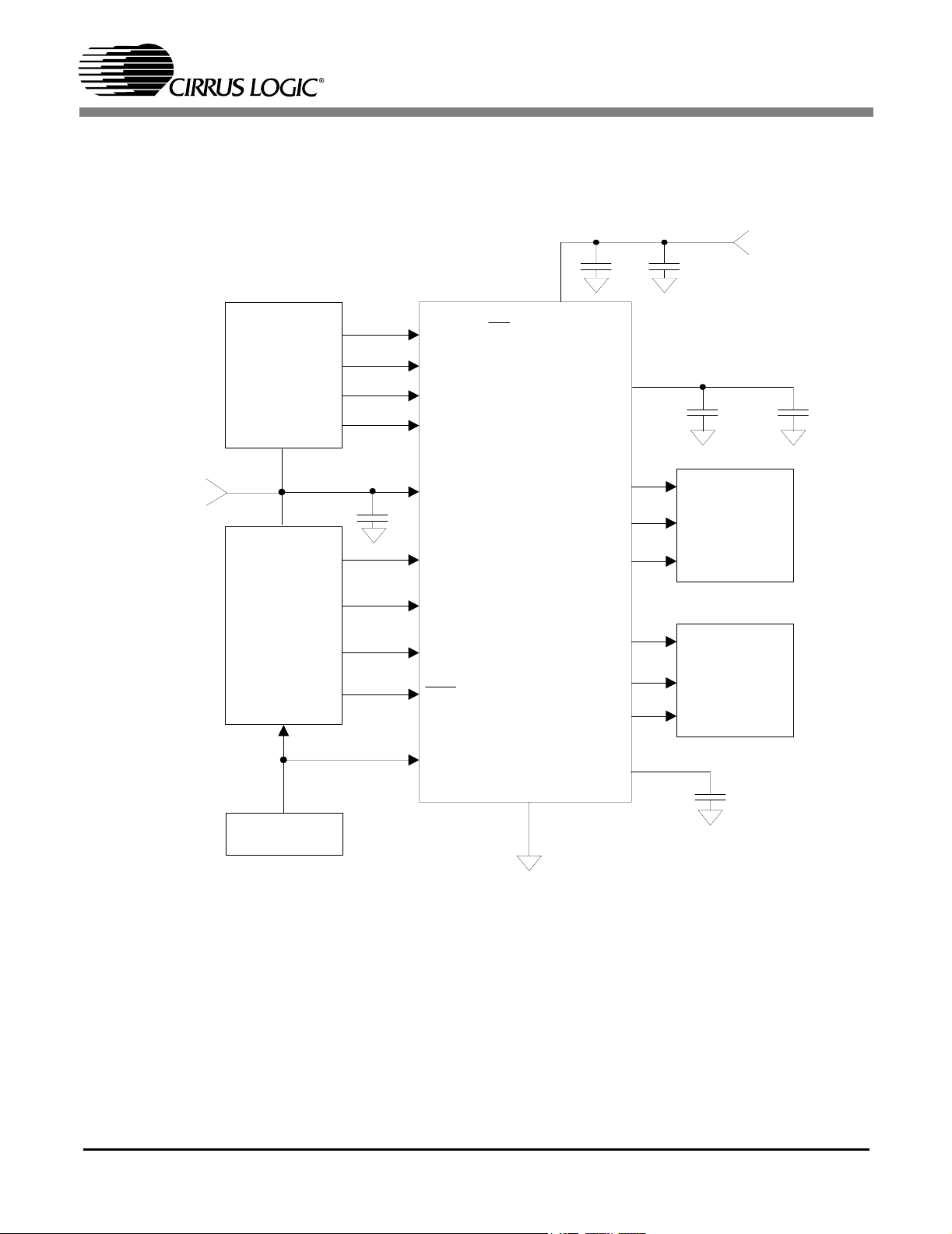
2. TYPICAL CONNECTION DIAGRAMS
CS4392
Logic Power
+5V to 1.8V
Mode
Select
(Control Port)
*
0.1 µf
Audio
Data
Processor
*
10
M0 (AD0/CS)
9
M1 (SDA/CDIN
8
M2 (SCL/CCLK)
7
M3
2
VL
5
LRCK
4
SCLK
3
SDATA
1
RST
17
)
CS4392
VA
AOUTA-
AMUTEC
AOUTA+
AOUTB-
BMUTEC
AOUTB+
0.1 µf
FILT+
11
19
20
18
14
13
15
µ
1.0
f+
0.1 µf 10 µf
Analog
Conditioning
&
Mute
Analog
Conditioning
&
Mute
+5V Analog
+
External Clock
6
MCLK
AGND
CMOUT
16
12
+
1.0 µf
Figure 1. Typical Connection Diagram - PCM Mode
* A high logic level for all digital inputs should not exceed VL.
DS459PP3 7
Page 8
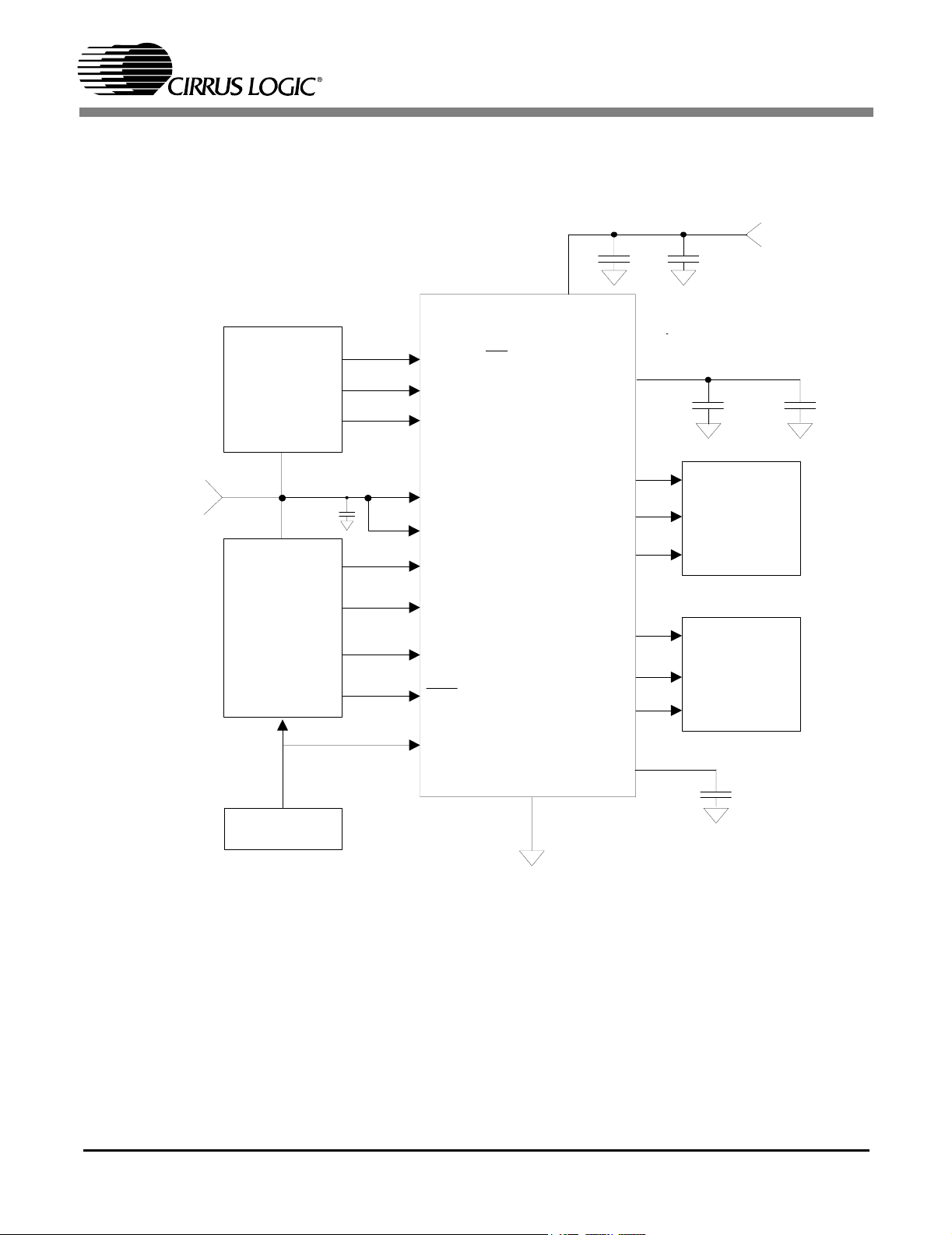
Logic Power
+5V to 1.8V
Mode
Select
(Control Port)
0.1 µf
10
M0 (AD0/CS)
9
M1 (SDA/CDIN)
8
M2 (SCL/CCLK)
2
VL
5
DSD_MODE
7
DSD_CLK
CS4392
17
VA
AMUTEC
FILT+
AOUTA-
AOUTA+
0.1 µf
19
20
18
11
CS4392
+5V Analog
µ
1.0
f+
0.1 µf 10 µf
Analog
Conditioning
&
Mute
+
Audio
Data
Processor
*
External Clock
4
3
1
6
DSD_B
DSD_A
RST
MCLK
AOUTB-
BMUTEC
AOUTB+
CMOUT
AGND
16
Figure 2. Typical Connection Diagram - DSD Mode
* A high logic level for all digital inputs should not exceed VL.
14
13
15
12
Analog
Conditioning
&
Mute
1.0 µf
+
8 DS459PP3
Page 9
CS4392
3. APPLICATIONS
3.1 Recommended Power-up Sequence for Hardware Mode
1) Hold RST low until the power supplies, master, and left/right clocks are stable.
2) Bring RST high. After 10ms the device will begin normal operation.
3.2 Recommended Power-up Sequence and Access to Control Port Mode
1) Hold RST low until the power supply, master, and left/right clocks are stable. In this state, the control
port is reset to its default settings and FILT+ will remain low.
2) Bring RST high. The device will remain in a low power state with FILT+ low and the control port is
accessible.
3) Write 30h to register 05h within 10 ms cycles following the release of RST. If after 10ms the control
port has not been initiated with this command, the device will enter stand-alone mode. The CPEN bit,
however, may be written at any time after 10ms. It is recommended to write CPEN before 10ms in order to reduce the possibility of any extraneous click or pop noise from occurring.
4) The desired register settings can be loaded while keeping the PDN bit set to 1.
5) Set the PDN bit to 0. This will initiate the power-up sequence which requires approximately 10 µS.
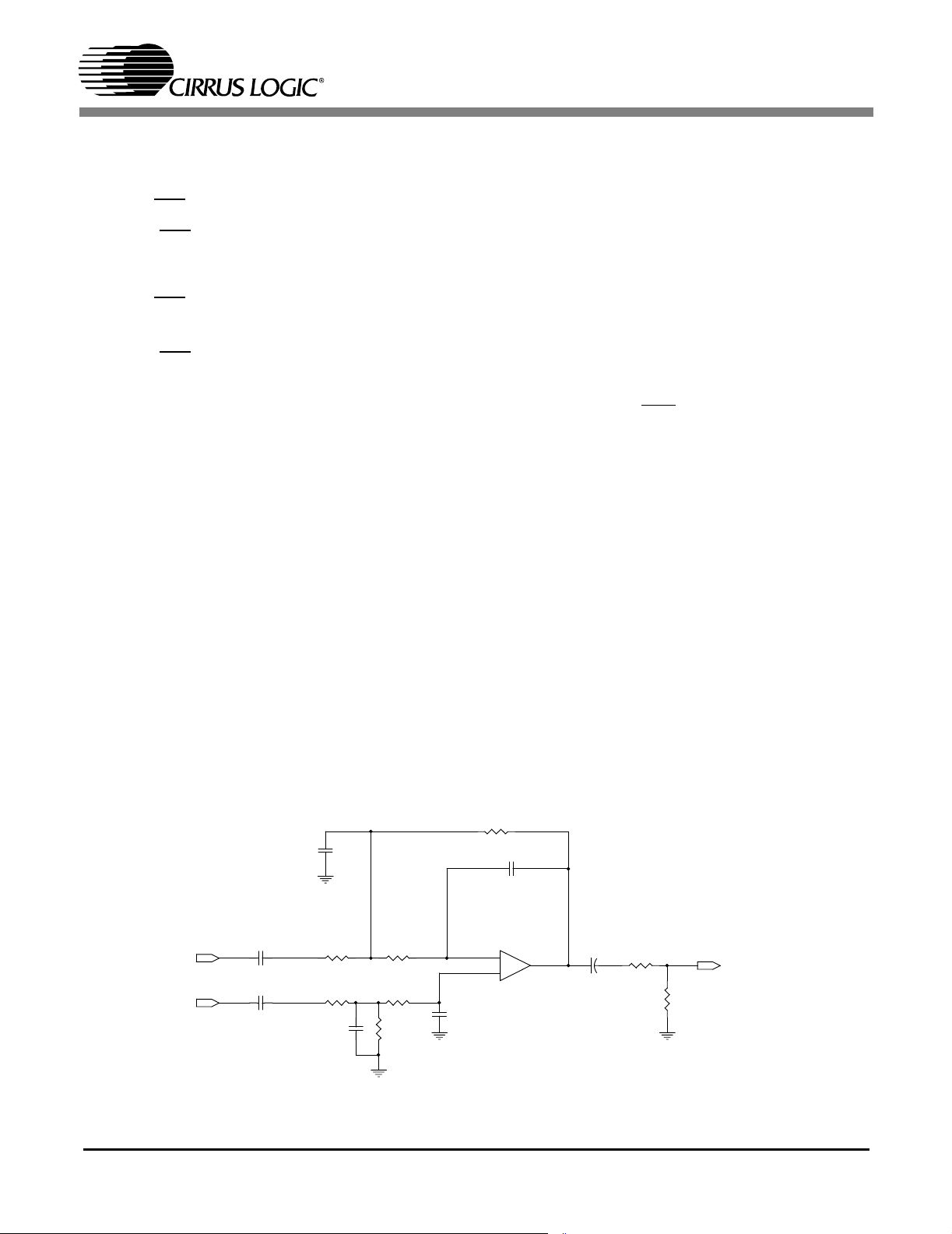
3.3 Analog Output and Filtering
The application note “Design Notes for a 2-Pole Filter with Differential Input” discusses the second-order
Butterworth filter and differential to single-ended converter as seen in Figure 3. An alternate configuration
can be seen on the CDB4392. This alternate filter configuration accounts for the differing AC loads on the
+ and - differential output pins which are normally present in a circuit like Figure 3. It also shows an AC
coupling configuration which reduces the number of required AC coupling capacitors to 2 caps per channel. The circuit in figure 3 may also be DC coupled, however the filter on the CDB4392 must be
AC coupled. The CS4392 is a linear phase design and does not include phase or amplitude compensation
for an external filter. Therefore, the DAC system phase and amplitude response will be dependent on the
external analog circuitry.
3.32k
2700 pF
680 pF
Aout -
Aout +
10 uF 560
10 uF
3.01k 1.58k
3.01k
2700 pF
R17
3.32k
1.58k
C10
680 pF
-
2
1
+
3
10 uF
Analog_Out
47k
Figure 3. CS4392 Output Filter
DS459PP3 9
Page 10
CS4392
3.4 Interpolation Filter
To accommodate the increasingly complex requirements of digital audio systems, the CS4392 incorporates selectable interpolation filters for each mode of operation. A fast and a slow roll-off filter is available
in each of Single, Double, and Quad Speed modes. These filters have been designed to accommodate a
variety of musical tastes and styles. Bit 5 of the Mode Control 3 register (06h) is used to select which filter
is used. Filter specifications can be found in Section 8, and filter response plots can be found in Figures 12
to 35.
In stand-alone mode, only the fast roll-off filter is available.
3.5 System Clocking
The required MCLK to LRCK and suggested SCLK to LRCK ratios are outlined in table 1. MCLK can be
at any phase in regards to LRCK and SCLK. SCLK, LRCK and SDATA must meet the phase and timing
relationships outlined in Section 7. Some common MCLK frequencies have been outlined in tables 2 to 4.
MCLK/LRCK SCLK/LRCK LRCK
Single Speed 256, 384, 512, 768, 1024* 32, 48, 64, 96, 128 Fs
Double Speed 128, 192, 256, 384, 512* 32, 48, 64 Fs
64 32 (16 bits only) Fs
Quad Speed
96 32, 48 Fs
128, 256* 32, 64 Fs
192 32, 48, 64, 96 Fs
Table 1. Clock Ratios
Sample Rate
(kHz)
32 8.1920 12.2880 16.3840 24.5760 32.7680
44.1 11.2896 16.9344 22.5792 33.8688 45.1584
48 12.2880 18.4320 24.5760 36.8640 49.1520
Sample Rate
(kHz)
64 8.1920 12.2880 16.3840 24.5760 32.7680
88.2 11.2896 16.9344 22.5792 33.8688 45.1584
96 12.2880 18.4320 24.5760 36.8640 49.1520
Sample Rate
(kHz)
176.4 11.2896 16.9344 22.5792 33.8688 45.1584
192 12.2880 18.4320 24.5760 36.8640 49.1520
*Note:These clocking ratios are only available in Control Port Mode when the MCLK Divide bit is enabled.
256x 384x 512x 768x 1024x*
Table 2. Single Speed (4 to 50 kHz sample rates) Common Clock Frequencies
128x 192x 256x 384x 512x*
Table 3. Double Speed (50 to 100 kHz sample rates) Common Clock Frequencies
64x 96x 128x 192x 256x*
Table 4. Quad Speed (100 to 200 kHz sample rates) Common Clock Frequencies
MCLK (MHz) See Note
MCLK (MHz) See Note
MCLK (MHz) See Note
10 DS459PP3
Page 11
CS4392
3.6 Digital Interface Format
The device will accept audio samples in several digital interface formats as illustrated in Tables 5 and 8.
The desired format is selected via the M0 and M1 pins for stand alone mode, and through the DIF2:0 bits
in the control port. For an illustration of the required relationship between the Left/Right Clock, Serial
Clock and Serial Audio Data, see Figures 4-6.
M1 M0 DESCRIPTION FORMAT FIGURE
00
01
10
11
LRCK
SCLK
Left Justified, up to 24-bit data
2
I
S, up to 24-bit data
Right Justified, 16-bit Data
Right Justified, 24-bit Data
Table 5. Digital Interface Format, Stand-Alone Mode Options
Left Channel
Right Channel
04
15
26
36
SDATA +3 +2 +1
MSB
-1 -2 -3 -4 -5
+5 +4
Figure 4. Format 0, Left Justified up to 24-Bit Data
LRCK
SCLK
SDATA +3 +2 +1
MSB
-1 -2 -3 -4 -5
Left Channel
+5 +4
Figure 5. Format 1, I2S up to 24-Bit Data
LRCK
SCLK
SDATA
LSB +5
Left Channel
MSB -1 -2 -3 -4 -5
32 clocks
-6
Figure 6. Format 2, Right Justified 16-Bit Data
Format 3, Right Justified 24-Bit Data
Format 4, Right Justified 20-Bit Data. (Available in Control Port Mode only)
Format 5, Right Justified 18-Bit Data. (Available in Control Port Mode only)
LSB
LSB
+6
+4 +3 +2
+5
+3 +2 +1
+3 +2 +1
-6
LSB
LSB
+6
+4 +3 +2
LSB
+1
MSB
-1 -2 -3 -4
MSB
-1 -2 -3 -4
LSB
+1
MSB
+5 +4
+5 +4
Right Channel
-1 -2 -3 -4
Right Channel
-5
DS459PP3 11
Page 12
CS4392
3.7 De-Emphasis
The device includes on-chip digital de-emphasis. Figure 7 shows the de-emphasis curve for FS equal to
44.1 kHz. The frequency response of the de-emphasis curve will scale proportionally with changes in sample rate, Fs. Please see Table 5 for the desired de-emphasis control for Stand-alone mode and Table 10 for
control port mode.
The de-emphasis feature is included to accommodate audio recordings that utilize 50/15 µS pre-emphasis
equalization as a means of noise reduction.
De-emphasis is only available in Single Speed Mode.
Gain
dB
T1=50 µs
0dB
T2 = 15 µs
-10dB
M2
(DEM)
0
1
Table 5. De-Emphasis Select, Stand-Alone Mode
DESCRIPTION FIGURE
No De-Emphasis
De-Emphasis Enabled
7
F1 F2
3.183 kHz 10.61 kHz
Figure 7. De-Emphasis Curve
Frequency
3.8 Oversampling Modes
The CS4392 operates in one of three oversampling modes based on the input sample rate. Mode selection
is determined by the M3 and M2 pins in Stand-Alone mode or the FM bits in Control Port mode. SingleSpeed mode supports input sample rates up to 50 kHz and uses a 128x oversampling ratio. Double-Speed
mode supports input sample rates up to 100 kHz and uses an oversampling ratio of 64x. Quad-Speed mode
supports input sample rates up to 200 kHz and uses an oversampling ratio of 32x
M3 M2 DESCRIPTION
00
01
10
11
Single-Speed without De-Emphasis (4 to 50 kHz sample rates)
Single-Speed with 44.1kHz De-Emphasis
Double-Speed (50 to 100 kHz sample rates)
Quad-Speed (100 to 200 kHz sample rates)
Table 6. Mode Selection, Stand-Alone Mode Options
12 DS459PP3
Page 13

CS4392
3.9 Using DSD mode
In stand-alone mode, DSD operation is selected by holding DSD_EN(LRCK) high and applying the DSD
data and clocks to the appropriate pins. The M2:0 pins set the expected DSD rate and MCLK ratio.
In control-port mode the FM bits set the device into DSD mode (DSD_EN pin is not required to be held
high). The DIF register then controls the expected DSD rate and MCLK ratio.
DSD_Mode M2 M1 M0 DESCRIPTION
1 000
1 001
1 010
1 011
1 100
1 101
1 110
1 111
Table 7. Direct Stream Digital (DSD), Stand-Alone Mode Options
3.10 Mute Control
64x oversampled DSD data with a 4x MCLK to DSD data rate
64x oversampled DSD data with a 6x MCLK to DSD data rate
64x oversampled DSD data with a 8x MCLK to DSD data rate
64x oversampled DSD data with a 12x MCLK to DSD data rate
128x oversampled DSD data with a 2x MCLK to DSD data rate
128x oversampled DSD data with a 3x MCLK to DSD data rate
128x oversampled DSD data with a 4x MCLK to DSD data rate
128x oversampled DSD data with a 6x MCLK to DSD data rate
The Mute Control pins go high during power-up initialization, reset, or if the Master Clock to Left Right
Clock ratio is incorrect. These pins will also go high following the reception of 8192 consecutive audio
samples of static 0 or -1 on both the left and right channels. A single sample of non-zero data on either
channel will cause the Mute Control pins to go low. These pins are intended to be used as control for an
external mute circuit in order to add off-chip mute capability.
Use of the Mute Control function is not mandatory but recommended for designs requiring the absolute
minimum in extraneous clicks and pops. Also, use of the Mute Control function can enable the system designer to achieve idle channel noise/signal-to-noise ratios which are only limited by the external mute circuit. See the CDB4392 data sheet for a suggested mute circuit.
DS459PP3 13
Page 14

CS4392
4. CONTROL PORT INTERFACE
The control port is used to load all the internal register settings (see section 6). The operation of the control
port may be completely asynchronous with the audio sample rate. However, to avoid potential interference
problems, the control port pins should remain static if no operation is required.
The control port operates in one of two modes: I2C
or SPI.
Notes: MCLK must be applied during all I2C communication.
4.0.1 MAP Auto Increment
The device has MAP (memory address pointer) auto increment capability enabled by the INCR bit
(also the MSB) of the MAP. If INCR is set to 0, MAP will stay constant for successive I2C writes
or reads, and SPI writes. If INCR is set to 1, MAP will auto increment after each byte is written,
allowing block reads or writes of successive registers.
4.0.2 I2C Mode
In the I2C mode, data is clocked into and out of the bi-directional serial control data line, SDA, by
the serial control port clock, SCL (see Figure 8 for the clock to data relationship). There is no CS
pin. Pin AD0 enables the user to alter the chip address (001000[AD0][R/W]) and should be tied to
VL or AGND as required, before powering up the device. If the device ever detects a high to low
transition on the AD0/CS pin after power-up, SPI mode will be selected.
4.0.2a I2C Write
To write to the device, follow the procedure below while adhering to the control port
Switching Specifications in section 7.
1) Initiate a START condition to the I2C bus followed by the address byte. The upper 6 bits
must be 001000. The seventh bit must match the setting of the AD0 pin, and the eighth must
be 0. The eighth bit of the address byte is the R/W bit.
2) Wait for an acknowledge (ACK) from the part, then write to the memory address pointer,
MAP. This byte points to the register to be written.
3) Wait for an acknowledge (ACK) from the part, then write the desired data to the register
pointed to by the MAP.
4) If the INCR bit (see section 4.0.1) is set to 1, repeat the previous step until all the desired
registers are written, then initiate a STOP condition to the bus.
5) If the INCR bit is set to 0 and further I2C writes to other registers are desired, it is necessary to initiate a repeated START condition and follow the procedure detailed from step
1. If no further writes to other registers are desired, initiate a STOP condition to the bus.
14 DS459PP3
Page 15

CS4392
4.0.2b I2C Read
To read from the device, follow the procedure below while adhering to the control port
Switching Specifications.
1) Initiate a START condition to the I2C bus followed by the address byte. The upper 6 bits
must be 001000. The seventh bit must match the setting of the AD0 pin, and the eighth must
be 1. The eighth bit of the address byte is the R/W bit.
2) After transmitting an acknowledge (ACK), the device will then transmit the contents of
the register pointed to by the MAP. The MAP register will contain the address of the last
register written to the MAP, or the default address (see section 4.1) if an I2C read is the first
operation performed on the device.
3) Once the device has transmitted the contents of the register pointed to by the MAP, issue
an ACK.
4) If the INCR bit is set to 1, the device will continue to transmit the contents of successive
registers. Continue providing a clock and issue an ACK after each byte until all the desired
registers are read, then initiate a STOP condition to the bus.
5) If the INCR bit is set to 0 and further I2C reads from other registers are desired, it is necessary to initiate a STOP condition and follow the procedure detailed from steps 1 and 2
from the I2C Write instructions followed by step 1 of the I2C Read section. If no further
reads from other registers are desired, initiate a STOP condition to the bus.
Note 1
ADDR
Start
001000
AD0
Figure 8. Control Port Timing, I2C Mode
SDA
SCL
Note : If o p eratio n is a w rite, th is by te c onta in s the M em ory A d dress P o inter, M A P .
R/W
ACK
DATA
1-8
ACK
DATA
1-8
ACK
Stop
DS459PP3 15
Page 16

CS4392
4.0.3 SPI Mode
In SPI mode, data is clocked into the serial control data line, CDIN, by the serial control port clock,
CCLK (see Figure 9 for the clock to data relationship). There is no AD0 pin. Pin CS is the chip
select signal and is used to control SPI writes to the control port. When the device detects a high to
low transition on the AD0/CS pin after power-up, SPI mode will be selected. All signals are inputs
and data is clocked in on the rising edge of CCLK.
4.0.3a SPI Write
To write to the device, follow the procedure below while adhering to the control port
Switching Specifications in section 7.
1) Bring CS low.
2) The address byte on the CDIN pin must then be 00100000.
3) Write to the memory address pointer, MAP. This byte points to the register to be written.
4) Write the desired data to the register pointed to by the MAP.
5) If the INCR bit (see section 4.0.1) is set to 1, repeat the previous step until all the desired
registers are written, then bring CS high.
6) If the INCR bit is set to 0 and further SPI writes to other registers are desired, it is necessary to bring CS high, and follow the procedure detailed from step 1. If no further writes
to other registers are desired, bring CS high.
CS
CCLK
CHIP
ADDRESS
CDIN
Figure 9. Control Port Timing, SPI mode
0010000
MAP = Memory Address Pointer
R/W
MAP
MSB
byte 1
DATA
LSB
byte n
4.1 Memory Address Pointer (MAP)
76543210
INCR Reserved Reserved Reserved MAP3 MAP2 MAP1 MAP0
00000000
4.1.1 INCR (AUTO MAP INCREMENT ENABLE)
Default = ‘0’
0 - Disabled,
1 - Enabled, the MAP will auto increment after each byte is written, allowing block reads or
writes of successive registers
the MAP will stay constant for successive writes
4.1.2 MAP3-0 (MEMORY ADDRESS POINTER)
Default = ‘0000’
16 DS459PP3
Page 17

CS4392
5. REGISTER QUICK REFERENCE
Addr Function 7 6 5 4 3 2 1 0
01h Mode Control 1 AMUTE DIF2 DIF1 DIF0 DEM1 DEM0 FM1 FM0
1000 0 0 00
02h Volume and
MIxing Control
03h Channel A
Volume Control
04h Channel B
Volume Control
05h Mode Control 2 INVERT_A INVERT_B CPEN PDN MUTEC A = B FREEZE MCLKDIV2 Reserved
06h Mode Control 3 Reserved Reserved Reserved FILT_SEL RMP_UP RMP_DN Reserved Reserved
07h Chip ID PART3 PART2 PART1 PART0 REV3 REV2 REV1 REV0
A = B Soft
0100 1 0 01
MUTE VOL6 VOL5 VOL4 VOL3 VOL2 VOL1 VOL0
0000 0 0 00
MUTE VOL6 VOL5 VOL4 VOL3 VOL2 VOL1 VOL0
0000 0 0 00
0001 0 0 00
0000 0 0 00
1000 - - - -
Zero
Cross
ATAPI4 ATAPI3 ATAPI2 ATAPI1 ATAPI0
DS459PP3 17
Page 18

CS4392
6. REGISTER DESCRIPTION
** All registers are read/write in Two-Wire mode and write only in SPI mode, unless otherwise noted**
6.1 Mode Control 1 - Address 01h
76543210
AMUTE DIF2 DIF1 DIF0 DEM1 DEM0 FM1 FM0
6.1.1 Auto-Mute (Bit 7)
Function:
The Digital-to-Analog converter output will mute following the reception of 8192 consecutive audio
samples of static 0 or -1. A single sample of non-static data will release the mute. Detection and
muting is done independently for each channel. (However, Auto-Mute detection and muting can become dependent on either channel if the Mute A = B function is enabled.) The common mode on the
output will be retained and the Mute Control pin for that channel will go active during the mute period.
The muting function is effected, similar to volume control changes, by the Soft and Zero Cross bits in
the Volume and Mixing Control register.
6.1.2 Digital Interface Formats (Bits 6:4)
Function:
PCM Mode - The required relationship between the Left/Right clock, serial clock and serial data is
defined by the Digital Interface Format and the options are detailed in Table 8 and Figures 4-6.
DIF2 DIF1 DIFO DESCRIPTION Format Figure
0 0 0 Left Justified, up to 24-bit data (default) 0 4
001
0 1 0 Right Justified, 16-bit Data 2 6
0 1 1 Right Justified, 24-bit Data 3 6
1 0 0 Right Justified, 20-bit Data 4 6
1 0 1 Right Justified, 18-bit Data 5 6
110 Reserved
111 Reserved
Table 8. Digital Interface Formats - PCM Modes
2
I
S, up to 24-bit data
15
18 DS459PP3
Page 19

DSD Mode - The relationship between the oversampling ratio of the DSD audio data and the required
Master clock to DSD data rate is defined by the Digital interface Format pins. Note that the Functional
Mode registers must be set to DSD Mode. See 9 for register options.
DIF2 DIF1 DIFO DESCRIPTION
0 0 0 64x oversampled DSD data with a 4x MCLK to DSD data rate (default)
0 0 1 64x oversampled DSD data with a 6x MCLK to DSD data rate
0 1 0 64x oversampled DSD data with a 8x MCLK to DSD data rate
0 1 1 64x oversampled DSD data with a 12x MCLK to DSD data rate
1 0 0 128x oversampled DSD data with a 2x MCLK to DSD data rate
1 0 1 128x oversampled DSD data with a 3x MCLK to DSD data rate
1 1 0 128x oversampled DSD data with a 4x MCLK to DSD data rate
1 1 1 128x oversampled DSD data with a 6x MCLK to DSD data rate
Table 9. Digital Interface Formats - DSD Mode
6.1.3 De-Emphasis Control (Bits 3:2)
Function:
Implementation of the standard 15 µs/50 µs digital de-emphasis filter response, Figure 7, requires reconfiguration of the digital filter to maintain the proper filter response for 32, 44.1 or 48 kHz sample
rates. NOTE: De-emphasis is available only in Single-Speed Mode. See 10 below.
DEM1 DEMO DESCRIPTION
0 0 Disabled (default)
0 1 44.1 kHz de-emphasis
1 0 48 kHz de-emphasis
1 1 32 kHz de-emphasis
Table 10. De-Emphasis Mode Selection
Gain
dB
T1=50 µs
0dB
-10dB
CS4392
T2 = 15 µs
F1 F2
3.183 kHz 10.61 kHz
Frequency
Figure 10. De-Emphasis Curve
6.1.4 Functional Mode (Bits 1:0)
Function:
Selects the required range of input sample rates or DSD Mode. See Table 11.
FM1 FM0 MODE
0 0 Single-Speed Mode: 4 to 50 kHz sample rates
(default)
0 1 Double-Speed Mode: 50 to 100 kHz sample rates
1 0 Quad-Speed Mode: 100 to 200 kHz sample rates
1 1 Direct Stream Digital Mode
Table 11. Functional Mode Selection
DS459PP3 19
Page 20

CS4392
6.2 Volume and Mixing Control (Address 02h)
76543210
A = B Soft Zero Cross ATAPI4 ATAPI3 ATAPI2 ATAPI1 ATAPI0
6.2.1 Channel A Volume = Channel B Volume (Bit 7)
Function:
The AOUTA and AOUTB volume levels are independently controlled by the A and the B Channel Volume Control Bytes when this function is disabled. The volume on both AOUTA and AOUTB are determined by the A Channel Volume Control Byte and the B Channel Byte is ignored when this function
is enabled.
6.2.2 Soft Ramp or Zero Cross Enable (Bits 6:5)
Function:
Soft Ramp Enable
Soft Ramp allows level changes, both muting and attenuation, to be implemented by incrementally
ramping, in 1/8 dB steps, from the current level to the new level at a rate of 1dB per 8 left/right clock
periods.
Zero Cross Enable
Zero Cross Enable dictates that signal level changes, either by attenuation changes or muting, will
occur on a signal zero crossing to minimize audible artifacts. The requested level change will occur
after a timeout period between 512 and 1024 sample periods (10.7 ms to 21.3 ms at 48 kHz sample
rate) if the signal does not encounter a zero crossing. The zero cross function is independently monitored and implemented for each channel.
Soft Ramp and Zero Cross Enable
Soft Ramp and Zero Cross Enable dictates that signal level changes, either by attenuation changes
or muting, will occur in 1/8 dB steps and be implemented on a signal zero crossing. The 1/8 dB level
change will occur after a timeout period between 512 and 1024 sample periods (10.7 ms to 21.3 ms
at 48 kHz sample rate) if the signal does not encounter a zero crossing. The zero cross function is
independently monitored and implemented for each channel. See Table 12
SOFT ZERO Mode
0 0 Changes to affect immediately
0 1 Zero Cross enabled
1 0 Soft Ramp enabled (default)
1 1 Soft Ramp and Zero Cross enabled
Table 12. Soft Cross or Zero Cross Mode Selection
6.2.3 ATAPI Channel Mixing and Muting (Bits 4:0)
Function:
The CS4392 implements the channel mixing functions of the ATAPI CD-ROM specification. See
Table 13 on page 21
20 DS459PP3
Page 21

CS4392
ATAPI4 ATAP I 3 ATAPI2 ATAPI1 ATAP I 0 A O U TA AOUTB
00000 MUTE MUTE
00001 MUTE bR
00010 MUTE bL
00011 MUTE b[(L+R)/2]
00100 aR MUTE
00101 aR bR
00110 aR bL
00111 aR b[(L+R)/2]
01000 aL MUTE
01001 aL bR
01010 aL bL
01011 aL b[(L+R)/2]
01100 a[(L+R)/2] MUTE
01101 a[(L+R)/2] bR
01110 a[(L+R)/2] bL
01111 a[(L+R)/2] b[(L+R)/2]
10000 MUTE MUTE
10001 MUTE bR
10010 MUTE bL
10011 MUTE [(bL+aR)/2]
10100 aR MUTE
10101 aR bR
10110 aR bL
10111 aR [(aL+bR)/2]
11000 aL MUTE
11001 aL bR
11010 aL bL
11011 aL [(aL+bR)/2]
11100 [(aL+bR)/2] MUTE
11101 [(aL+bR)/2] bR
11110 [(bL+aR)/2] bL
1 1 1 1 1 [(aL+bR)/2] [(aL+bR)/2]
Table 13. ATAPI Decode
Left Channel
Audio Data
A Channel
Volume
Control
MUTE
AoutA
ΣΣ
Right Channel
Audio Data
Figure 11. ATAPI Block Diagram
DS459PP3 21
B Channel
Volume
Control
MUTE
AoutB
Page 22

CS4392
6.3 Channel A Volume Control - Address 03h
See 4.4 Channel B Volume Control - Address 04h
6.4 CHANNEL B VOLUME CONTROL - ADDRESS 04H
76543210
MUTE VOL6 VOL5 VOL4 VOL3 VOL2 VOL1 VOL0
6.4.1 Mute (Bit 7)
Function:
The Digital-to-Analog converter output will mute when enabled. The common mode voltage on the
output will be retained. The muting function is effected, similiar to attenuation changes, by the Soft
and Zero Cross bits in the Volume and Mixing Control register. The MUTEC pin for that channel will
go active during the mute period if the Mute function is enabled. Both the AMUTEC and BMUTEC
will go active if either MUTE register is enabled and the MUTEC A = B bit (register 5) is enabled.
6.4.2 Volume Control (Bits 6:0)
Function:
The digital volume control allows the user to attenuate the signal in 1 dB increments from 0 to -127 dB.
Volume settings are decoded as shown in Table 14. The volume changes are implemented as dictated
by the Soft and Zero Cross bits in the Volume and Mixing Control register (see section 6.2.2).
Binary Code Decimal Value Volume Setting
0000000 0 0 dB
0010100 20 -20 dB
0101000 40 -40 dB
0111100 60 -60 dB
1011010 90 -90 dB
Table 14. Digital Volume Control Example Settings
6.5 Mode Control 2 - Address 05h
76543210
INVERT_A INVERT_B CPEN PDN MUTEC A = B FREEZE MCLKDIV2 Reserved
6.5.1 Invert Signal Polarity (Bits 7:6)
Function:
When set to 1, this bit inverts the signal polarity for the appropriate channel. This is useful if a board
layout error has occurred, or an other situations where a 180 degree phase shift is desirable. Default
is 0.
22 DS459PP3
Page 23

6.5.2 Control Port Enable (Bit 5)
Function:
This bit defaults to 0, allowing the device to power-up in Stand-Alone mode. The Control port mode
can be accessed by setting this bit to 1. This will allow the operation of the device to be controlled by
the registers and the pin definitions will conform to Control Port Mode. To accomplish a clean powerup, the user should write 30h to register 5 within 10 ms following the release of Reset.
6.5.3 Power Down (Bit 4)
Function:
The device will enter a low-power state whenever this function is activated (set to 1). The power-down
bit defaults to ‘enabled’ (1) on power-up and must be disabled before normal operation will begin. The
contents of the control registers are retained when the device is in power-down.
6.5.4 AMUTEC = BMUTEC (Bit 3)
Function:
When this function is enabled, the individual controls for AMUTEC and BMUTEC are internally connected through a AND gate prior to the output pins. Therefore, the external AMUTEC and BMUTEC
pins will go active only when the requirements for both AMUTEC and BMUTEC are valid.
CS4392
6.5.5 Freeze (Bit 2)
Function:
This function allows modifications to the control port registers without the changes taking effect until
Freeze is disabled. To make multiple changes in the Control port registers take effect simultaneously,
set the Freeze Bit, make all register changes, then Disable the Freeze bit.
6.5.6 Master Clock Divide (Bit 1)
Function:
This function allows the user to select an internal divide by 2 of the Master Clock. This selection is
required to access the higher Master Clock rates as shown in Tables 2 through 4 on page 10.
6.6 Mode Control 3 - Address 06h
B7 B6 B5 B4 B3 B2 B1 B0
Reserved Reserved Reserved FILT_SEL RMP_UP RMP_DN Reserved Reserved
6.6.1 Interpolation Filter Select (Bit 4)
Function:
This Function allows the user to select whether the Interpolation Filter has a fast (set to 0 - default) or
slow (set to 1) roll off. The - 3dB corner is approximately the same for both filters, but the slope of
the roll of is greater for the ‘fast’ roll off filter.
DS459PP3 23
Page 24

6.6.2 Soft Volume Ramp-up after Reset (Bit 3)
Function:
This function allows the user to control whether a soft ramp up in volume is applied when reset is released either by the reset pin or internal to the chip. The modes are as follows:
0 - An instantaneous change is made from max attenuation to the control port volume setting on release of reset (default setting).
1 - Volume is ramped up using the soft-ramp settings in Bits 6:5 of register 02h (see 6.2.2) from max
attenuation to the control port volume setting on release of reset.
6.6.3 Soft Ramp-down before Reset (Bit 2)
Function:
This function allows the user to control if a soft ramp-down in volume is applied before a known reset
condition. The modes are as follows:
0 - An instantaneous change is made from the control port volume setting to max attenuation when
chip resets (default setting).
1 - Volume is ramped down using the soft-ramp settings in Bits 6:5 of register 02h (see 6.2.2) from
the control port volume setting to max attenuation when chip resets.
CS4392
6.7 Chip ID - Register 07h
B7 B6 B5 B4 B3 B2 B1 B0
PART3 PART2 PART1 PART0 REV3 REV2 REV1 REV0
Function:
This register is Read-Only. Bits 7 through 4 are the part number ID which is 1000b (8h) and the remaining Bits (3 through 0) are for the chip revision.
24 DS459PP3
Page 25

CS4392
7. CHARACTERISTICS/SPECIFICATIONS
ANALOG CHARACTERISTICS (CS4392-KS/KZ/KZZ) ((Test conditions (unless otherwise
specified): Input test signal is a 997 Hz sine wave at 0 dBFS; measurement bandwidth is 10 Hz to 20 kHz; test load
=3kΩ, CL = 10 pF. Typical performance characteristics are derived from measurements taken at TA = 25 °C,
R
L
VL = VA = 5.0V. Min/Max performance characteristics are guaranteed over the specified operating temperature
and voltages.)
VA = 5.0V
Parameter
Dynamic Performance for All Speed Modes and DSD
Dynamic Range
(Note 1) unweighted
A-Weighted
Total Harmonic Distortion + Noise
(Note 1) 0 dB
-20 dB
-60 dB
Idle Channel Noise / Signal-to-Noise Ratio - 114 - dB
Interchannel Isolation (1 kHz) - 100 - dB
DC Accuracy
Interchannel Gain Mismatch ICGM - 0.1 - dB
Gain Drift - 100 - ppm/°C
Analog Output Characteristics and Specifications
Full Scale Differential Output Voltage V
Output Resistance
(Note 2) Z
Minimum AC-Load Resistance R
Maximum Load Capacitance C
Symbol Min Typ Max Unit
105
108
THD+N -
-
-
0.95xVA 0.99xVA 1.05xVA Vpp
FS
out
L
L
- 100 - Ω
-3-kΩ
- 100 - pF
111
114
-100
-91
-51
-
-
-94
-
-45
dB
dB
dB
dB
dB
Notes: 1. One-half LSB of Triangular PDF dither is added to data.
2. V
is tested under load RL but does not include attenuation due to Z
FS
OUT
DS459PP3 25
Page 26

CS4392
COMBINED INTERPOLATION & ON-CHIP ANALOG FILTER RESPONSE (The
filter characteristics and the X-axis of the response plots have been normalized to the sample rate (Fs) and can be
referenced to the desired sample rate by multiplying the given characteristic by Fs.)
Fast Roll-Off
Parameter
Single-Speed Mode - (4 kHz to 50 kHz sample rates)
Passband to -0.01 dB corner
to -3 dB corner
Frequency Response 10 Hz to 20 kHz -0.01 - +0.01 dB
StopBand 0.547 - - Fs
StopBand Attenuation
Group Delay - 12/Fs - s
Passband Group Delay Deviation 0 - 20 kHz - - ±0.41/Fs s
De-emphasis Error (Relative to 1kHz) Fs = 32 kHz
(Note 5) Fs = 44.1 kHz
Double-Speed Mode - (50 kHz to 100 kHz sample rates)
Passband to -0.01 dB corner
to -3 dB corner
Frequency Response 10 Hz to 20 kHz -0.01 - 0.01 dB
StopBand 0.583 - - Fs
StopBand Attenuation
Group Delay - 4.6/Fs - s
Passband Group Delay Deviation 0 - 20 kHz - - ±0.03/Fs s
Quad Speed Mode - (100 kHz to 200 kHz)
Passband to -0.01 dB corner
to -3 dB corner
Frequency Response 10 Hz to 20 kHz -0.01 - 0.01 dB
StopBand 0.635 - - Fs
StopBand Attenuation
Group Delay - 4.7/Fs - s
Passband Group Delay Deviation 0 - 20 kHz - - ±0.01/Fs s
DSD Mode
Passband to -0.1 dB corner
to -3 dB corner
Frequency Response 10 Hz to 20 kHz -.01 - 0.1 dB
(Note 4) 90 - - dB
Fs = 48 kHz
(Note 4) 80 - - dB
(Note 4) 90 - - dB
0
0
-
-
-
0
0
0
0
0
0
-
-
-
-
-
-
-
-
-
-
-
0.454
0.499
±0.23
±0.14
±0.09
0.430
0.499
0.105
0.490
20
120
UnitMin Typ Max
Fs
Fs
dB
dB
dB
Fs
Fs
Fs
Fs
kHz
kHz
26 DS459PP3
Page 27

CS4392
COMBINED INTERPOLATION & ON-CHIP ANALOG FILTER RESPONSE (Cont.)
Slow Roll-Off
Parameter
Single-Speed Mode - (4 kHz to 50 kHz sample rates)
Passband to -0.01 dB corner
to -3 dB corner
Frequency Response 10 Hz to 20 kHz -0.01 - +0.01 dB
StopBand 0.583 - - Fs
StopBand Attenuation
Group Delay - 6.5/Fs - s
Passband Group Delay Deviation 0 - 20 kHz - ±0.14/Fs s
De-emphasis Error (Relative to 1kHz) Fs = 32 kHz
(Note 5) Fs = 44.1 kHz
Double-Speed Mode - (50 kHz to 100 kHz sample rates)
Passband to -0.01 dB corner
to -3 dB corner
Frequency Response 10 Hz to 20 kHz -0.01 - 0.01 dB
StopBand 0.792 - - Fs
StopBand Attenuation
Group Delay - 3.9/Fs - s
Passband Group Delay Deviation 0 - 20 kHz - ±0.01/Fs s
Quad Speed Mode - (100 kHz to 200 kHz)
Passband to -0.01 dB corner
to -3 dB corner
Frequency Response 10 Hz to 20 kHz -0.01 - 0.01 dB
StopBand 0.868 - - Fs
StopBand Attenuation
Group Delay - 4.2/Fs - s
Passband Group Delay Deviation 0 - 20 kHz - ±0.01/Fs s
DSD Mode
Passband to -0.1 dB corner
to -3 dB corner
Frequency Response 10 Hz to 20 kHz -.01 - 0.1 dB
(Note 4) 64 - - dB
Fs = 48 kHz
(Note 4) 70 - - dB
(Note 4) 75 - - dB
0
0
-
-
-
0
0
0
0
0
0
-
-
-
-
-
-
-
-
-
-
-
(Note 3)
0.417
0.499
±0.23
±0.14
±0.09
0.296
0.499
0.104
0.481
20
120
UnitMin Typ Max
Fs
Fs
dB
dB
dB
Fs
Fs
Fs
Fs
kHz
kHz
Notes: 3. Slow Roll-Off interpolation filter is only available in control port mode.
4. For Single and Double-Speed Mode, the Measurement Bandwidth is from stopband to 3 Fs.
For Quad-Speed Mode, the Measurement Bandwidth is from stopband to 1.34 Fs.
5. De-emphasis is only available in Single Speed Mode; The 44.1kHz De-emphasis filter is the only filter
available in Stand-Alone Mode.
DS459PP3 27
Page 28

CS4392
0
20
40
60
Amplitude (dB)
80
100
120
0.4 0.5 0.6 0.7 0.8 0.9 1
Frequency(normalized to Fs)
0
20
40
60
Amplitude (dB)
80
100
120
0.4 0.42 0.44 0.46 0.48 0.5 0.52 0.54 0.56 0.58 0.6
Frequency(normalized to Fs)
Figure 12. Single Speed (fast) Stopband Rejection Figure 13. Single Speed (fast) Transition Band
0
1
2
3
4
5
Amplitude (dB)
6
7
8
9
10
0.45 0.46 0.47 0.48 0.49 0.5 0.51 0.52 0.53 0.54 0.55
Frequency(normalized to Fs)
0.02
0.015
0.01
0.005
0
Amplitude (dB)
0.005
0.01
0.015
0.02
0 0.05 0.1 0.15 0.2 0.25 0.3 0.35 0.4 0.45 0.5
Frequency(normalized to Fs)
Figure 14. Single Speed (fast) Transition Band (detail) Figure 15. Single Speed (fast) Passband Ripple
0
20
40
60
Amplitude (dB)
80
100
120
0.4 0.5 0.6 0.7 0.8 0.9 1
Frequency(normalized to Fs)
0
20
40
60
Amplitude (dB)
80
100
120
0.4 0.42 0.44 0.46 0.48 0.5 0.52 0.54 0.56 0.58 0.6
Frequency(normalized to Fs)
Figure 16. Single Speed (slow) Stopband Rejection Figure 17. Single Speed (slow) Transition Band
28 DS459PP3
Page 29

CS4392
0
1
2
3
4
5
Amplitude (dB)
6
7
8
9
10
0.45 0.46 0.47 0.48 0.49 0.5 0.51 0.52 0.53 0.54 0.55
Frequency(normalized to Fs)
0.02
0.015
0.01
0.005
0
Amplitude (dB)
0.005
0.01
0.015
0.02
0 0.05 0.1 0.15 0.2 0.25 0.3 0.35 0.4 0.45 0.5
Frequency(normalized to Fs)
Figure 18. Single Speed (slow) Transition Band (detail) Figure 19. Single Speed (slow) Passband Ripple
0
20
40
60
Amplitude (dB)
80
0
20
40
60
Amplitude (dB)
80
100
120
0.4 0.5 0.6 0.7 0.8 0.9 1
Frequency(normalized to Fs)
100
120
0.4 0.42 0.44 0.46 0.48 0.5 0.52 0.54 0.56 0.58 0.6
Frequency(normalized to Fs)
Figure 20. Double Speed (fast) Stopband Rejection Figure 21. Double Speed (fast) Transition Band
0
1
2
3
4
5
Amplitude (dB)
6
7
8
9
10
0.45 0.46 0.47 0.48 0.49 0.5 0.51 0.52 0.53 0.54 0.55
Frequency(normalized to Fs)
0.02
0.015
0.01
0.005
0
Amplitude (dB)
0.005
0.01
0.015
0.02
0 0.05 0.1 0.15 0.2 0.25 0.3 0.35 0.4 0.45 0.5
Frequency(normalized to Fs)
Figure 22. Double Speed (fast) Transition Band (detail) Figure 23. Double Speed (fast) Passband Ripple
DS459PP3 29
Page 30

CS4392
0
20
40
60
Amplitude (dB)
80
100
120
0.2 0.3 0.4 0.5 0.6 0.7 0.8 0.9 1
Frequency(normalized to Fs)
0
20
40
60
Amplitude (dB)
80
100
120
0.2 0.3 0.4 0.5 0.6 0.7 0.8
Frequency(normalized to Fs)
Figure 24. Double Speed (slow) Stopband Rejection Figure 25. Double Speed (slow) Transition Band
0
1
2
3
4
5
Amplitude (dB)
6
7
8
9
10
0.45 0.46 0.47 0.48 0.49 0.5 0.51 0.52 0.53 0.54 0.55
Frequency(normalized to Fs)
0.02
0.015
0.01
0.005
0
Amplitude (dB)
0.005
0.01
0.015
0.02
0 0.05 0.1 0.15 0.2 0.25 0.3 0.35
Frequency(normalized to Fs)
Figure 26. Double Speed (slow) Transition Band (detail) Figure 27. Double Speed (slow) Passband Ripple
0
20
40
60
Amplitude (dB)
80
100
120
0.2 0.3 0.4 0.5 0.6 0.7 0.8 0.9 1
Frequency(normalized to Fs)
0
20
40
60
Amplitude (dB)
80
100
120
0.2 0.3 0.4 0.5 0.6 0.7 0.8
Frequency(normalized to Fs)
Figure 28. Quad Speed (fast) Stopband Rejection Figure 29. Quad Speed (fast) Transition Band
30 DS459PP3
Page 31

CS4392
0
1
2
3
4
5
Amplitude (dB)
6
7
8
9
10
0.45 0.46 0.47 0.48 0.49 0.5 0.51 0.52 0.53 0.54 0.55
Frequency(normalized to Fs)
0.2
0.15
0.1
0.05
0
Amplitude (dB)
0.05
0.1
0.15
0.2
0 0.05 0.1 0.15 0.2 0.25
Frequency(normalized to Fs)
Figure 30. Quad Speed (fast) Transition Band (detail) Figure 31. Quad Speed (fast) Passband Ripple
0
20
40
60
Amplitude (dB)
80
0
20
40
60
Amplitude (dB)
80
100
120
0.1 0.2 0.3 0.4 0.5 0.6 0.7 0.8 0.9 1
Frequency(normalized to Fs)
100
120
0.1 0.2 0.3 0.4 0.5 0.6 0.7 0.8 0.9
Frequency(normalized to Fs)
Figure 32. Quad Speed (slow) Stopband Rejection Figure 33. Quad Speed (slow) Transition Band
0
1
2
3
4
5
Amplitude (dB)
6
7
8
9
10
0.45 0.46 0.47 0.48 0.49 0.5 0.51 0.52 0.53 0.54 0.55
Frequency(normalized to Fs)
0.02
0.015
0.01
0.005
0
Amplitude (dB)
0.005
0.01
0.015
0.02
0 0.02 0.04 0.06 0.08 0.1 0.12
Frequency(normalized to Fs)
Figure 34. Quad Speed (slow) Transition Band (detail) Figure 35. Quad Speed (slow) Passband Ripple
DS459PP3 31
Page 32

CS4392
SWITCHING CHARACTERISTICS - SERIAL AUDIO INTERFACE
(Inputs: Logic 0 = 0 V, Logic 1 = VL) .
Parameters Symbol Min Typ Max Units
Input Sample Rate Fs 4 - 200 kHz
LRCK Duty Cycle 45 50 55 %
MCLK Duty Cycle 40 50 60 %
SCLK Frequency Single Speed Mode
Double Speed Mode
Quad Speed Mode (MCLKDIV=0)
Quad Speed Mode (MCLKDIV=1)
SCLK rising to LRCK edge delay t
SCLK rising to LRCK edge setup time t
SDATA valid to SCLK rising setup time t
SCLK rising to SDATA hold time t
slrd
slrs
sdlrs
sdh
-
-
-
-
-
-
-
-
20 - - ns
20 - - ns
20 - - ns
20 - - ns
128•LRCK
64•LRCK
MCLK/2
MCLK/4
Hz
Hz
Hz
Hz
LRCK
SCLK
SDATA
t
t
slrd
t
sdlrs
slrs
t
sdh
Figure 36. Serial Mode Input Timing
32 DS459PP3
Page 33

CS4392
SWITCHING SPECIFICATIONS - DSD INTERFACE (Logic 0 = AGND; Logic 1 = VL)
Parameter Symbol Min Max Unit
MCLK Duty Cycle 40 60 %
DSD_SCLK Pulse Width Low t
DSD_SCLK Pulse Width High t
DSD_SCLK Period t
DSD_L or DSD_R valid to DSD_SCLK rising setup time t
DSD_SCLK rising to DSD_L or DSD_R hold time t
t
sclkh
t
sclkl
sclkl
sclkh
sclkw
sdlrs
sdh
20 - ns
20 - ns
20
-ns
20 - ns
20 - ns
DSD_SCLK
t
sdlrstsdh
DSD_L, DSD_R
Figure 37. Direct Stream Digital - Serial Audio Input Timing
DS459PP3 33
Page 34

SWITCHING CHARACTERISTICS - CONTROL PORT INTERFACE
(Inputs: logic 0 = AGND, logic 1 = VL)
Parameter Symbol Min Max Unit
2
I
C Mode
SCL Clock Frequency f
Rising Edge to Start t
RST
Bus Free Time Between Transmissions t
Start Condition Hold Time (prior to first clock pulse) t
Clock Low time t
Clock High Time t
Setup Time for Repeated Start Condition t
SDA Hold Time from SCL Falling (Note 6) t
SDA Setup time to SCL Rising t
Rise Time of Both SDA and SCL Lines t
Fall Time of Both SDA and SCL Lines t
Setup Time for Stop Condition t
scl
irs
buf
hdst
low
high
sust
hdd
sud
r
f
susp
- 100 kHz
500 - ns
4.7 - µs
4.0 - µs
4.7 - µs
4.0 - µs
4.7 - µs
0-µs
250 - ns
-1µs
-300ns
4.7 - µs
CS4392
Notes: 6. Data must be held for sufficient time to bridge the 300 ns transition time of SCL.
RST
t
SDA
SCL
irs
Stop S ta r t
t
buf
t
t
hdst
low
t
hdd
t
high
t
sud
Repeated
Start
t
t
sust
hdst
t
f
t
r
Figure 38. I2C Mode Control Port Timing
Stop
t
susp
34 DS459PP3
Page 35

CS4392
SWITCHING CHARACTERISTICS - SPI CONTROL PORT (Inputs: logic 0 = AGND,
logic 1 = VL)
Parameter Symbol Min Max Unit
SPI Mode
CCLK Clock Frequency f
Rising Edge to CS Falling t
RST
CCLK Edge to CS
CS
High Time Between Transmissions t
Falling to CCLK Edge t
CS
Falling (Note 7) t
CCLK Low Time t
CCLK High Time t
CDIN to CCLK Rising Setup Time t
CCLK Rising to DATA Hold Time (Note 8) t
Rise Time of CCLK and CDIN (Note 9) t
Fall Time of CCLK and CDIN (Note 9) t
sclk
srs
spi
csh
css
scl
sch
dsu
dh
r2
f2
-6MHz
500 - ns
500 - ns
1.0 - µs
20 - ns
82 - ns
82 - ns
40 - ns
15 - ns
-100ns
-100ns
Notes: 7. t
8. Data must be held for sufficient time to bridge the transition time of CCLK.
9. For F
only needed before first falling edge of CS after RST rising edge. t
spi
< 1 MHz
SCK
RST
CS
CCLK
CDIN
t
srs
t
t
css
spi
t
r2
t
t
scl
sch
t
f2
t
t
dsu
dh
= 0 at all other times.
spi
t
csh
Figure 39. SPI Control Port Timing
DS459PP3 35
Page 36

CS4392
DC ELECTRICAL CHARACTERISTICS (AGND = 0V; all voltages with respect to AGND.)
Parameter Symbol Min Typ Max Units
Normal Operation
Power Supply Current All Supplies=5.0V IA + I
Power Dissipation - 130 150 mW
Power-Down Mode
Power Supply Current All Supplies=5.0V IA + I
Power Dissipation - 1.5 - mW
All Modes of Operation
Power Supply Rejection Ratio
Common Mode Voltage
Output Impedance
Maximum allowable DC current source/sink
Filt+ Nominal Voltage
Output Impedance
Maximum allowable DC current source/sink
MUTEC Low-Level Output Voltage - 0 - V
MUTEC High-Level Output Voltage - VA - V
Maximum MUTEC Drive Current - 3 - mA
(Note 10)
(Note 11)
(Note 12) (1 kHz)
(60 Hz)
L
L
PSRR -
CMOUT -
-2630mA
-300- µA
-
-
-
-
-
-
60
40
0.48•VA
250
0.001
VA
250
0.001
-
-
-
-
-
-
-
-
dB
dB
V
kΩ
mA
V
kΩ
mA
Notes: 10. Normal operation is defined as RST = HI with a 997 Hz, 0dBFS input sampled at Fs = 48kHz, and open
outputs, unless otherwise stated.
11. Power-Down Mode is defined as RST
12. Valid with the recommended capacitor values on FILT+ and VQ as shown in Figures 1 and 2.
= LO with all clocks and data lines held static.
DIGITAL INPUT CHARACTERISTICS & SPECIFICATIONS (AGND = 0V; all voltages
with respect to AGND.)
Parameters Symbol Min Typ Max Units
Input Leakage Current I
Input Capacitance - 8 - pF
High-Level Input Voltage
Low-Level Input Voltage
in
V
IH
V
IL
--±10µA
70% - - VL
-20%VL
THERMAL CHARACTERISTICS AND SPECIFICATIONS
Parameters Symbol Min Typ Max Units
Package Thermal Resistance CS4392-KS
CS4392-KZ/KZZ
Ambient Operating Temperature (Power Applied) T
θJA
θJA
A
-
-
-10 - +70 °C
68
72
-
-
°C/Watt
°C/Watt
36 DS459PP3
Page 37

CS4392
RECOMMENDED OPERATING SPECIFICATIONS (AGND = 0V; all voltages with respect
to AGND.)
Parameters Symbol Min Typ Max Units
DC Power Supply VA
VL
ABSOLUTE MAXIMUM RATINGS (AGND = 0 V; all voltages with respect to ground.)
Parameters Symbol Min Max Units
DC Power Supply VA
VL
Input Current, Any Pin Except Supplies I
Digital Input Voltage V
Ambient Operating Temperature (power applied) T
Storage Temperature T
WARNING: Operation at or beyond these limits may result in permanent damage to the device. Normal operation is
not guaranteed at these extremes.
in
IND
A
stg
4.75
1.8
-0.3
-0.3
-0.3 VL+0.4 V
-55 125 °C
-65 150 °C
5.0
-
-±10mA
6.0
VA
5.25
VA
V
V
V
V
DS459PP3 37
Page 38

8. PARAMETER DEFINITIONS
Total Harmonic Distortion + Noise (THD+N)
The ratio of the rms value of the signal to the rms sum of all other spectral components over the specified
bandwidth (typically 10Hz to 20kHz), including distortion components. Expressed in decibels.
Dynamic Range
The ratio of the full scale rms value of the signal to the rms sum of all other spectral components over the
specified bandwidth. Dynamic range is a signal-to-noise measurement over the specified bandwidth
made with a -60 dBFS signal. 60 dB is then added to the resulting measurement to refer the measurement
to full scale. This technique ensures that the distortion components are below the noise level and do not
effect the measurement. This measurement technique has been accepted by the Audio Engineering Society, AES17-1991, and the Electronic Industries Association of Japan, EIAJ CP-307.
Interchannel Isolation
A measure of crosstalk between the left and right channels. Measured for each channel at the converter's
output with all zeros to the input under test and a full-scale signal applied to the other channel. Units in
decibels.
Interchannel Gain Mismatch
The gain difference between left and right channels. Units in decibels.
CS4392
Gain Error
The deviation from the nominal full scale analog output for a full scale digital input.
Gain Drift
The change in gain value with temperature. Units in ppm/°C.
9. REFERENCES
1. CDB4392 Evaluation Board Datasheet
2. “The I
2
http://www.semiconductors.philips.com
C-Bus Specification: Version 2.1” Philips Semiconductors, January 2000.
38 DS459PP3
Page 39

10.PACKAGE DIMENSIONS
20L TSSOP (4.4 mm BODY) PACKAGE DRAWING
N
CS4392
1
23
TOP VIEW
D
E
e
2
b
SIDE VIEW
A2
A1
A
SEATING
PLANE
L
INCHES MILLIMETERS
1
E1
END VIEW
NOT
DIM MIN NOM MAX MIN NOM MAX
A -- -- 0.043 -- -- 1.10
A1 0.002 0.004 0.006 0.05 -- 0.15
A2 0.03346 0.0354 0.037 0.85 0.90 0.95
b 0.00748 0.0096 0.012 0.19 0.245 0.30 2,3
D 0.252 0.256 0.259 6.40 6.50 6.60 1
E 0.248 0.2519 0.256 6.30 6.40 6.50
E1 0.169 0.1732 0.177 4.30 4.40 4.50 1
e -- -- 0.026 -- -- 0.65
L 0.020 0.024 0.028 0.50 0.60 0.70
∝
0° 4° 8° 0° 4° 8°
∝
E
JEDEC #: MO-153
Controlling Dimension is Millimeters.
Notes: 1. “D” and “E1” are reference datums and do not included mold flash or protrusions, but do include mold
mismatch and are measured at the parting line, mold flash or protrusions shall not exceed 0.20 mm per
side.
2. Dimension “b” does not include dambar protrusion/intrusion. Allowable dambar protrusion shall be
0.13 mm total in excess of “b” dimension at maximum material condition. Dambar intrusion shall not
reduce dimension “b” by more than 0.07 mm at least material condition.
3. These dimensions apply to the flat section of the lead between 0.10 and 0.25 mm from lead tips.
DS459PP3 39
Page 40

PACKAGE DIMENSIONS(cont.).
20L SOIC (300 MIL BODY) PACKAGE DRAWING
1
b
CS4392
HE
c
D
SEATING
PLANE
A
e
A1
L
INCHES MILLIMETERS
DIM MIN NOM MAX MIN NOM MAX
A 0.093 0.098 0.104 2.35 2.50 2.65
A1 0.004 0.008 0.012 0.10 0.20 0.30
b 0.013 0.017 0.020 0.33 0.43 0.51
C 0.009 0.011 0.013 0.23 0.28 0.32
D 0.496 0.504 0.512 12.60 12.80 13.00
E 0.291 0.295 0.299 7.40 7.50 7.60
e 0.040 0.050 0.060 1.02 1.27 1.52
H 0.394 0.407 0.419 10.00 10.34 10.65
L 0.016 0.025 0.050 0.40 0.64 1.27
∝ 0° 4° 8° 0° 4° 8°
JEDEC #: MS-013
Controlling Dimension is Millimeters
∝
40 DS459PP3
 Loading...