

Page 1
CS4391A
24-Bit, 192 kHz Stereo DAC with Volume Control
Features
Complete Stereo DAC System: Interpolation,
D/A, Output Analog Filtering
108 dB Dynamic Range
94 dB THD+N
Direct Stream Digital Mode
Low Clock Jitter Sensitivity
+5 V Power Supply
ATAPI Mixing
On-Chip Digital De-emphasis for 32, 44.1,
and 48 kHz
Volume Control with Soft Ramp
– 119 dB Attenuation
– 1 dB Step Size
– Zero Crossing Click-Free Transitions
Direct Interface with 5 V to 1.8 V Logic
I
M1
(SDA/CDIN)
M3
M2
(SCL/CCLK) (AD0/CS)
Description
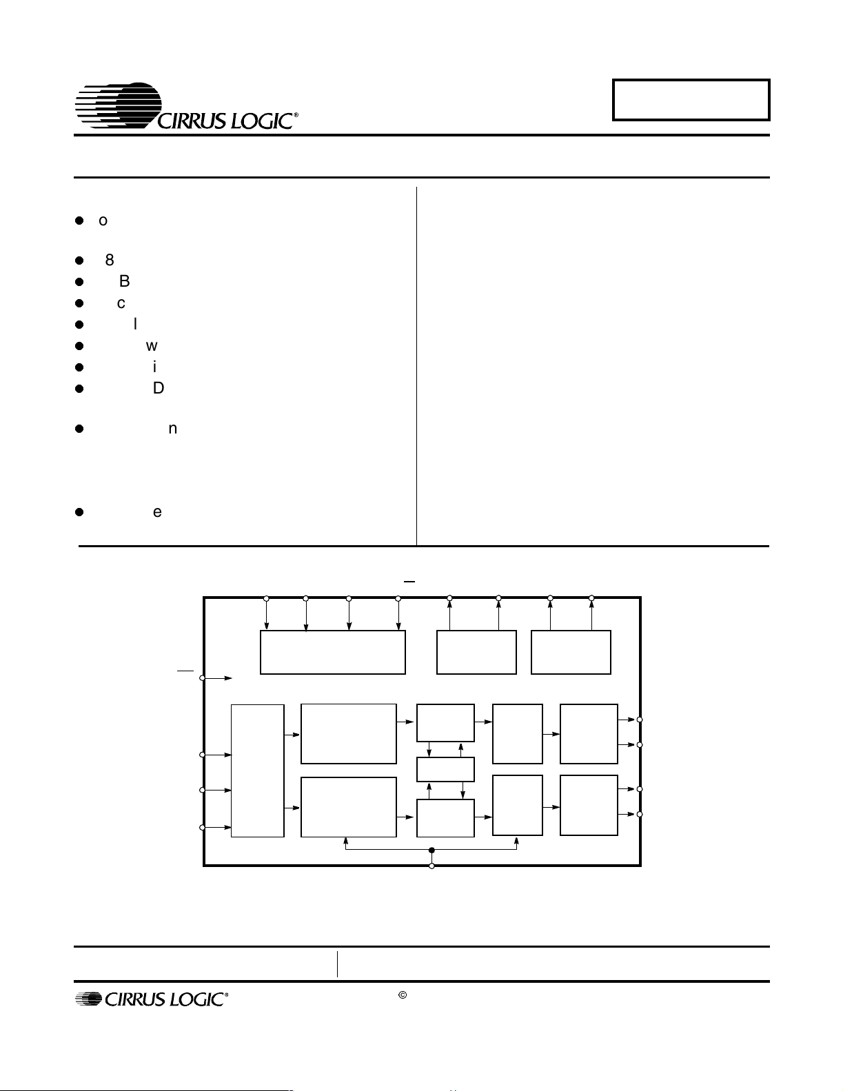
The CS4391A is a complete stereo digital-to-analog system including digital interpolation, fourth-order deltasigma digital-to-analog conversion, digital de-emphasis,
volume control, channel mixing and analog filtering. The
advantages of this architecture include: ideal differential
linearity, no distortion mechanisms due to resistor
matching errors, no linearity drift over time and temperature and a high tolerance to clock jitter.
The CS4391A accepts PCM data at sample rates from
4 kHz to 192 kHz, DSD audio data, consumes very little
power and operates over a wide power supply range.
These features are ideal for DVD, A/V receivers, CD and
set-top box systems.
ORDERING INFORMATION
CS4391A-KS 20-pin SOIC -10 to 70 °C
CS4391A-KZ 20-pin TSSOP -10 to 70 °C
CS4391A-KZZ 20-pin TSSOP, Lead Free -10 to 70 °C
CDB4391A Evaluation Board
M0
AMUTEC
CMOUT
FILT+BMUTEC
MODE SELECT
(CONTROL PORT)
RST
SCLK
LRCK
SDATA
SERIAL
PORT
Preliminary Product Information
www.cirrus.com
INTERPOLATION
FILTER
INTERPOLATOR
FILTER
MUTE CONTROL
VOLUM E
CONTROL
MIXER
VOLUM E
CONTROL
MCLK
EXTERNAL
∆Σ
DAC
∆Σ
DAC
REFERENCE
ANALOG
FILTER
ANALOG
FILTER
This document contains information for a new product.
Cirrus Logic reserves the right to modify this product without notice.
Copyright © Cirrus Logic, Inc. 20 04
(All Rights Reserved)
AOUTA+
AOUTA-
AOUTB+
AOUTB-
JUL ‘04
DS600PP3
1
Page 2

TABLE OF CONTENTS
1. CHARACTERISTICS/SPECIFICATIONS ................................................................................. 5
2. TYPICAL CONNECTION DIAGRAMS ...................................................................................13
3. REGISTER QUICK REFERENCE ..........................................................................................15
3.1 Mode Control 1 (address 01h) .......................................................................................... 15
3.2 Volume and Mixing Control (address 02h)........................................................................ 16
3.3 Channel A Volume Control (address 03h) ........................................................................ 16
3.4 Channel B Volume Control (address 04h) ........................................................................ 16
3.5 Mode Control 2 (address 05h) .......................................................................................... 17
4. REGISTER DESCRIPTION .................................................................................................... 18
4.1 Mode Control 1 - Address 01h .......................................................................................... 18
4.1.1 Auto-Mute (Bit 7) ................................................................................................. 18
4.1.2 Digital Interface Formats (Bits 6:4) ...................................................................... 18
4.1.3 De-Emphasis Control (Bits 3:2) ........................................................................... 18
4.1.4 Functional Mode (Bits 1:0) .................................................................................. 18
4.2 Volume and Mixing Control (Address 02h) .......................................................................19
4.2.1 Channel A Volume = Channel B Volume (Bit 7) ................................................. 19
4.2.2 Soft Ramp or Zero Cross Enable (Bits 6:5) ......................................................... 19
4.2.3 ATAPI Channel Mixing and Muting (Bits 4:0) ...................................................... 19
4.3 Channel A Volume Control - Address 03h........................................................................ 19
4.4 Channel B Volume Control - Address 04h .......................................................................20
4.4.1 Mute (Bit 7) .......................................................................................................... 20
4.4.2 Volume Control (Bits 6:0) .................................................................................... 20
4.5 Mode Control 2 - Address 05h .......................................................................................... 20
4.5.1 Invert Signal Polarity (Bits 7:6) ............................................................................ 20
4.5.2 Control Port Enable (Bit 5) .................................................................................. 20
4.5.3 Power Down (Bit 4) .............................................................................................20
4.5.4 AMUTEC = BMUTEC (Bit 3) ............................................................................... 20
4.5.5 Freeze (Bit 2) ...................................................................................................... 21
4.5.6 Master Clock Divide (Bit 1) .................................................................................. 21
CS4391A
Contacting Cirrus Logic Support
For all product questions and inquiries contact a Cirrus Logic Sales Representative.
To find one nearest you go to http://www.cirrus.com
IMPORTANT NOTICE
"Preliminary" product information describes products that are in production, but for which full characterization data is not yet available. "Advance" product information describes products that are in development and subject to development changes. Cirrus Logic, Inc. and its subsidiaries ("Cirrus") beli eve that the information contai ned in this document is accurate and rel iable. However, the information is subject to change without notice and is provided "AS IS" without warranty
of any kind (express or implied). Customers are advised to obtain the latest version of relevant information to veri fy, before placing orders, that information being
relied on is current and complete. All products are sold subject to the terms and condi tions of sale supplied at the time of order acknowledgment, including those
pertaining to warranty, patent infringement, and limitati on of liabil ity. No responsibility is assumed by Cirrus for the use of thi s infor mation, i ncluding use of this
information as the basis for manufacture or sale of any items, or for infringement of patents or other rights of third parties. Thi s document is the property of Cirrus
and by furni shing this information, Cirrus grants no license, express or impli ed under any patents, mask work rights, copyrights, trademarks, trade secrets or
other intellectual property rights. Cirrus owns the copyri ghts associated with the information contained herein and gives consent for copies to be made of the
information only for use within your organi zation with respect to Cirrus integrated circuits or other parts of Cirrus. This consent does not extend to other copying
such as copying for general distri bution, advertising or promotional purposes, or for creating any work for resale.
An export permit needs to be obtai ned from the competent authorities of the Japanese Government if any of the products or technologies described in thi s material and controlled under the "Foreign Exchange and Foreign Trade Law" is to be exported or taken out of Japan. An export li cense and/or quota needs to be
obtained f rom the competent author ities of t he Chinese Government if any of the products or tec hnologies describ ed in this mater ial is subj ect to the PRC Forei gn
Trade Law and is to be exported or taken out of the PRC.
CERTAIN APPLICATIONS USING SEMICONDUCTOR PRODUCTS MAY INVOLVE POTENTIAL RISKS OF DEATH, PERSONAL INJURY, OR SEVERE
PROPERTY OR ENVIRONMENTAL DAMAGE ("CRITICAL APPLICATIONS"). CIRRUS PRODUCTS ARE NOT DESIGNED, AUTHORIZED, OR WARRANTED TO BE SUITABLE FOR USE I N LIFE-SUPPORT DEVICES OR SYSTEMS OR OTHER CRITICAL APPLICATIONS. INCLUSION OF CIRRUS PRODUCTS
IN SUCH APPLICATIONS IS UNDERSTOOD TO BE FULLY AT THE CUSTOMER'S RISK.
Purchase of I
those components in a standard I
Cirrus Logic, Cirrus, and the Ci rrus Logic logo designs are trademarks of Cirrus Logic, Inc. All other brand and product names in this document may be trademarks or servi ce marks of their respective owners.
2 DS600PP3
2
C components of Cirrus Logic, Inc., or one of its sublicensed Associated Companies conveys a license under the Phillips I2C Patent Rights to use
2
C system.
Page 3

5. PIN DESCRIPTION - PCM DATA MODE ............................................................................... 22
6. PIN DESCRIPTION - DSD MODE .......................................................................................... 26
7. APPLICATIONS ..................................................................................................................... 33
7.1 Recommended Power-up Sequence for Hardware Mode ............................................... 33
7.2 Recommended Power-up Sequence and Access to Control Port Mode ......................... 33
7.3 Analog Output and Filtering ............................................................................................. 33
8. CONTROL PORT INTERFACE .............................................................................................. 34
8.1 SPI Mode ......................................................................................................................... 34
8.2 I2C Mode ......................................................................................................................... 34
9. PARAMETER DEFINITIONS .................................................................................................. 38
10. REFERENCES ...................................................................................................................... 38
11. PACKAGE DIMENSIONS ................................................................................................. 39
LIST OF TABLES
Table 1. Digital Interface Formats - PCM Modes ................................................................................ 27
Table 2. Digital Interface Formats - DSD Mode...................................................................................27
Table 3. De-Emphasis Mode Selection .............................................................................................. 27
Table 4. Functional Mode Selection .................................................................................................... 27
Table 5. Soft Cross or Zero Cross Mode Selection............................................................................ 27
Table 6. ATAPI Decode....................................................................................................................... 28
Table 7. Digital Volume Control........................................................................................................... 28
Table 8. Single Speed (4 to 50 kHz sample rates) Common Clock Frequencies................................ 29
Table 9. Double Speed (50 to 100 kHz sample rates) Common Clock Frequencies ......................... 29
Table 10. Quad Speed (100 to 200 kHz sample rates) Common Clock Frequencies ........................ 29
Table 11. Single Speed (4 to 50 kHz) Digital Interface Format, Stand-Alone Mode Options .............. 29
Table 12. Single Speed Only (4 to 50 kHz) De-Emphasis, Stand-Alone Mode Options ..................... 29
Table 13. Double Speed (50 to 100 kHz) Digital Interface Format, Stand-Alone Mode Options......... 29
Table 14. Quad Speed (100 to 200 kHz) Digital Interface Format, Stand-Alone Mode Options ......... 30
Table 15. Direct Stream Digital (DSD), Stand-Alone Mode Options ................................................... 30
Table 16. Memory Address Pointer (MAP)..........................................................................................35
CS4391A
DS600PP3 3
Page 4

LIST OF FIGURES
Figure 1. Serial Mode Input Timing ................................................................................................. 9
Figure 2. Direct Stream Digital - Serial Audio Input Timing........................................................... 10
Figure 3. I
Figure 4. SPI Control Port Timing ................................................................................................. 12
Figure 5. Typical Connection Diagram - PCM Mode.....................................................................13
Figure 6. Typical Connection Diagram - DSD Mode ..................................................................... 14
Figure 7. Format 0, Left Justified up to 24-Bit Data....................................................................... 31
Figure 8. Format 1, I2S up to 24-Bit Data .....................................................................................31
Figure 9. Format 2, Right Justified 16-Bit Data ............................................................................. 31
Figure 10. Format 3, Right Justified 24-Bit Data ........................................................................... 31
Figure 11. Format 4, Right Justified 20-Bit Data. (Available in Control Port Mode only).............. 32
Figure 12. Format 5, Right Justified 18-Bit Data. (Available in Control Port Mode only)............... 32
Figure 13. De-Emphasis Curve..................................................................................................... 32
Figure 14. ATAPI Block Diagram ..................................................................................................32
Figure 15. CS4391A Output Filter .................................................................................................33
Figure 16. Control Port Timing, SPI mode ....................................................................................35
Figure 17. Control Port Timing, I
Figure 18. Single-Speed Frequency Response ............................................................................ 36
Figure 19. Single-Speed Transition Band .....................................................................................36
Figure 20. Single-Speed Transition Band .....................................................................................36
Figure 21. Single-Speed Stopband Rejection ............................................................................... 36
Figure 22. Double-Speed Frequency Response ........................................................................... 36
Figure 23. Double-Speed Transition Band .................................................................................... 36
Figure 24. Double-Speed Transition Band .................................................................................... 37
Figure 25. Double-Speed Stopband Rejection .............................................................................. 37
2
C Control Port Timing .................................................................................................. 11
CS4391A
2
C Mode .....................................................................................35
4 DS600PP3
Page 5
CS4391A
1. CHARACTERISTICS/SPECIFICATIONS
(Min/Max performance characteristics and specifications are guaranteed over the Specified Operating Conditions.
Typical performance characteristics are derived from measurements taken at T
SPECIFIED OPERATING CONDITIONS (AGND = 0V; all voltages with respect to ground.)
Parameters Symbol Min Typ Max Units
DC Power Supply VA
VL
Specified Temperature Range -KS & -KZ T
ABSOLUTE MAXIMUM RATINGS (AGND = 0 V; all voltages with respect to ground.)
Parameters Symbol Min Max Units
DC Power Supply VA
Input Current, Any Pin Except Supplies I
Digital Input Voltage V
Ambient Operating Temperature (power applied) T
Storage Temperature T
WARNING: Operation at or beyond these limits may result in permanent damage to the device. Normal operation is
not guaranteed at these extremes.
A
VL
in
IND
A
stg
= 25 °C, VA = 5.0 V)
A
4.75
1.8
-10 - 70 °C
-0.3
-0.3
-0.3 VL+0.4 V
-55 125 °C
-65 150 °C
5.0
-
-±10mA
6.0
VA
5.25
VA
V
V
V
V
DS600PP3 5
Page 6
CS4391A
ANALOG CHARACTERISTICS (Test conditions (unless otherwise specified): Input test signal is a
997 Hz sine wave at 0 dBFS; measurement bandwidth is 10 Hz to 20 kHz; Test load R
Parameter
Symbol Min Typ Max Unit
Dynamic Performance
Dynamic Range (Note 1)
unweighted
A-Weighted
40 kHz Bandwidth A-Weighted
Total Harmonic Distortion + Noise (Note 1,2)
THD+N
0 dB
-20 dB
-60 dB
Idle Channel Noise / Signal-to-Noise Ratio - 108 - dB
Interchannel Isolation (1 kHz) - 100 - dB
Power Supplies
Power Supply Current normal operation
power-down state
I
+ I
A
IA + I
L
L
Power Dissipation
normal operation
power-down
Power Supply Rejection Ratio (1 kHz) (Note 3)
PSRR -
(60 Hz)
= 5 kΩ, CL = 10 pF)
L
VA = 5 V
100
103
-
-
-
-
-
-
-
-
105
108
102
-94
-85
-45
17
60
85
0.3
60
-
40
-
-
-
-89
-
-40
35
-
dB
dB
dB
dB
dB
dB
mA
µA
175-mW
mW
-
-
dB
dB
Parameter Symbol Min Typ Max Units
Analog Ou tput
Full Scale Differential Output Voltage 1.05VA 1.1VA 1.15VA Vpp
Common Mode Voltage CMOUT - 0.43VA - VDC
Interchannel Gain Mismatch - 0.1 - dB
Gain Drift - 100 - ppm/°C
AC-Load Resistance R
Load Capacitance C
L
L
5--kΩ
- - 100 pF
6 DS600PP3
Page 7
CS4391A
ANALOG CHARACTERISTICS (continued)
Parameter Symbol Min Typ Max Unit
Combined Digital and On-chip Analog Filter Response - Single Speed Mode
Passband (Note 3)
to -0.05 dB corner
to -3 dB corner
Frequency Response 10 Hz to 20 kHz -.02 - +.035 dB
StopBand .5465 - - Fs
StopBand Attenuation (Note 5) 50 - - dB
Group Delay tgd - 9/Fs - s
Passband Group Delay Deviation 0 - 20 kHz - ±0.36/Fs - s
De-emphasis Error (Relative to 1 kHz)
Control Port Mode Fs = 32 kHz
Fs = 44.1 kHz
Fs = 48 kHz
Stand-Alone Mode Fs = 44.1 kHz
Combined Digital and On-chip Analog Filter Response - Double Speed Mode
Passband (Note 4)
to -0.1 dB corner
to -3 dB corner
Frequency Response 10 Hz to 20 kHz -0.1 - 0 dB
StopBand .577 - - Fs
StopBand Attenuation (Note 5) 55 - - dB
Group Delay tgd - 9/Fs - s
Passband Group Delay Deviation 0 - 20 kHz - ±0.23/Fs - s
On-chip Analog Filter Response - Quad Speed Mode
Passband (Note 4)
to -3 dB corner 0 - 0.25 Fs
Frequency Response 10 Hz to 20 kHz -0.7 - 0 dB
On-chip Analog Filter Response - DSD Mode
Passband (Note 4)
to -3 dB corner 0 - 1.0 Fs
Frequency Response 10 Hz to 20 kHz -0.7 - 0 dB
Notes: 1. Triangular PDF dithered data.
2. THD+N specifications for 48 kHz sample rates are made over a 20 kHz Bandwidth.
3. Valid with the recommended capacitor values on FILT+ and CMOUT as shown in Figure 1. Increasing
the capacitance will also increase the PSRR.
4. Response is clock dependent and will scale with Fs. Note that the response plots (Figures 18-25) have
been normalized to Fs and can be de-normalized by multiplying the X-axis scale by Fs.
5. For Single-Speed Mode, the Measurement Bandwidth is 0.5465 Fs to 3 Fs.
For Double-Speed Mode, the Measurement Bandwidth is 0.577 Fs to 1.4 Fs.
0
0
-
-
-
-
0
0
-
-
-
-
-
-
-
-
.4535
.4998
+.2/-.1
+.05/-.14
+0/.22
+.05/-.14
.4621
.4982
Fs
Fs
dB
dB
dB
dB
Fs
Fs
DS600PP3 7
Page 8
CS4391A
DIGITAL CHARACTERISTICS (AGND = 0 V; all voltages with respect to ground.)
Parameters Symbol Min Typ Max Units
High-Level Input Voltage
Low-Level Input Voltage
Input Leakage Current I
Input Capacitance - 8 - pF
Maximum MUTEC Drive Current - 3 - mA
V
IH
V
IL
in
70% - - VL
- 20% VL
--±10µA
8 DS600PP3
Page 9

CS4391A
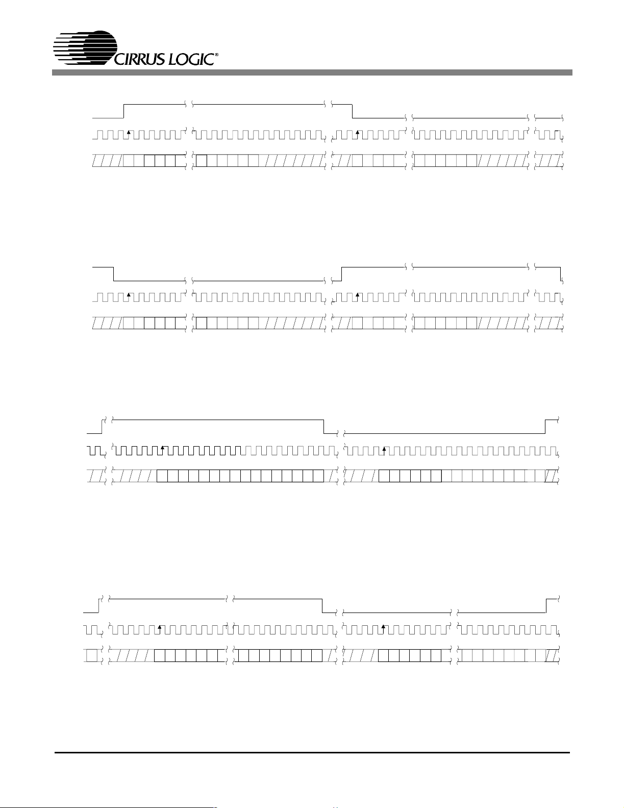
SWITCHING CHARACTERISTICS - PCM MODES (Inputs: Logic 0 = 0 V, Logic 1 = VL)
Parameters Symbol Min Typ Max Units
Input Sample Rate Fs 4 - 200 kHz
LRCK Duty Cycle 45 50 55 %
MCLK Duty Cycle 40 50 60 %
SCLK Frequency
SCLK Frequency (Note 6)
SCLK rising to LRCK edge delay t
SCLK rising to LRCK edge setup time t
SDATA valid to SCLK rising setup time t
SCLK rising to SDATA hold time t
slrd
slrs
sdlrs
sdh
-
-
20 - - ns
20 - - ns
20 - - ns
20 - - ns
Notes: 6. This serial clock is available only in Control Port Mode when the MCLK Divide bit is enabled.
-MCLK/2Hz
-MCLK/4Hz
LRCK
SCLK
SDATA
t
t
slrd
t
sdlrs
slrs
t
sdh
Figure 1. Serial Mode Input Timing
DS600PP3 9
Page 10
CS4391A
SWITCHING CHARACTERISTICS - DSD (Logic 0 = AGND = DGND; Logic 1 = VL)
Parameter Symbol Min Typ Max Unit
MCLK Duty Cycle 40 50 60 %
SCLK Pulse Width Low t
SCLK Pulse Width High t
SCLK Period t
SDIN valid to SCLK rising setup time t
SCLK rising to SDIN hold time t
sclkl
sclkh
sclkw
sdlrs
sdh
t
sclkl
20 - - ns
20 - - ns
20
--ns
20 - - ns
20 - - ns
t
sclkh
SCLK
t
sdlrstsdh
SDATA
Figure 2. Direct Stream Digital - Serial Audio Input Timing
10 DS600PP3
Page 11
CS4391A
SWITCHING CHARACTERISTICS - I2C CONTROL PORT (Inputs: logic 0 = AGND,
logic 1 = VL)
Parameter Symbol Min Max Unit
2C®
Mode
I
SCL Clock Frequency f
RST
Rising Edge to Start t
Bus Free Time Between Transmissions t
Start Condition Hold Time (prior to first clock pulse) t
Clock Low time t
Clock High Time t
Setup Time for Repeated Start Condition t
SDA Hold Time from SCL Falling (Note 7) t
SDA Setup time to SCL Rising t
Rise Time of Both SDA and SCL Lines t
Fall Time of Both SDA and SCL Lines t
Setup Time for Stop Condition t
scl
irs
buf
hdst
low
high
sust
hdd
sud
r
f
susp
-100KHz
500 - ns
4.7 - µs
4.0 - µs
4.7 - µs
4.0 - µs
4.7 - µs
0-µs
250 - ns
-1µs
- 300 ns
4.7 - µs
Notes: 7. Data must be held for sufficient time to bridge the 300 ns transition time of SCL.
RST
t
SDA
SCL
irs
Stop S tart
t
buf
t
hdst
t
low
t
hdd
t
high
t
sud
Repeated
Start
t
t
sust
hdst
t
f
t
r
Figure 3. I2C Control Port Timing
Stop
t
susp
DS600PP3 11
Page 12
CS4391A
SWITCHING CHARACTERISTICS - SPI CONTROL PORT (Inputs: logic 0 = AGND,
logic 1 = VL)
Parameter Symbol Min Max Unit
SPI Mode
CCLK Clock Frequency f
RST
Rising Edge to CS Falling t
CCLK Edge to CS
CS
High Time Between Transmissions t
CS
Falling to CCLK Edge t
Falling (Note 8) t
CCLK Low Time t
CCLK High Time t
CDIN to CCLK Rising Setup Time t
CCLK Rising to DATA Hold Time (Note 9) t
Rise Time of CCLK and CDIN (Note 10) t
Fall Time of CCLK and CDIN (Note 10) t
sclk
srs
spi
csh
css
scl
sch
dsu
dh
r2
f2
-6MHz
500 - ns
500 - ns
1.0 - µs
20 - ns
66 - ns
66 - ns
40 - ns
15 - ns
- 100 ns
- 100 ns
Notes: 8. t
9. Data must be held for sufficient time to bridge the transition time of CCLK.
10. For F
only needed before first falling edge of CS after RST rising edge. t
spi
< 1 MHz
SCK
RST
CS
CCLK
CDIN
t
srs
t
t
css
spi
t
r2
t
t
sch
scl
t
f2
t
t
dsu
dh
= 0 at all other times.
spi
t
csh
Figure 4. SPI Control Port Timing
12 DS600PP3
Page 13
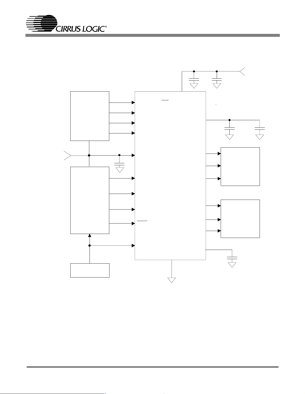
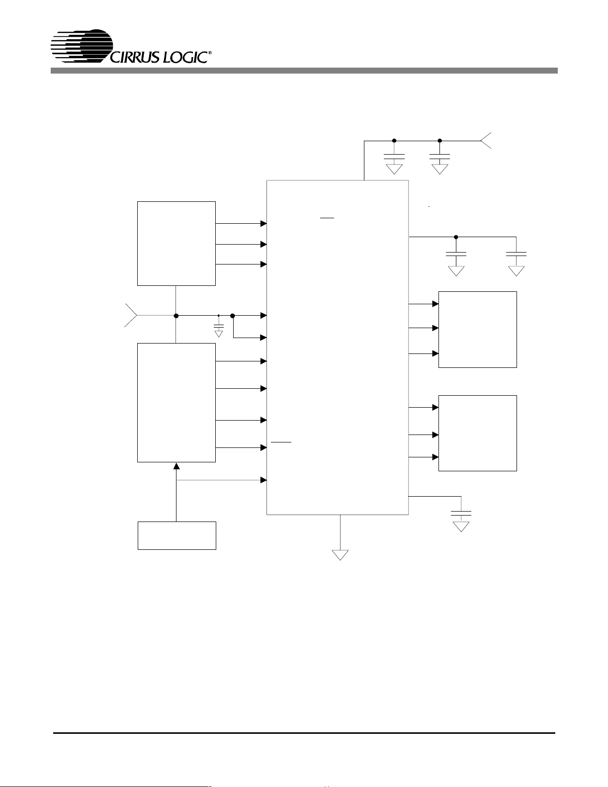
2. TYPICAL CONNECTION DIAGRAMS
CS4391A
Logic Power
+5V to 1.8V
Mode
Select
(Control Port)
*
0.1 µf
Audio
Data
Processor
*
10
M0 (AD0/CS)
9
M1 (SDA/
8
M2 (SCL/CCLK)
7
M3
2
VL
5
LRCK
4
SCLK
3
SDATA
1
RST
17
VA
CDIN
)
CS4391A
0.1 µf
FILT+
AOUTA-
AMUTEC
AOUTA+
AOUTB-
BMUTEC
AOUTB+
11
19
20
18
14
13
15
µ
+
f
1.0
0.1 µf 1.0 µf
Analog
Conditioning
&
Mute
Analog
Conditioning
&
Mute
+5V Analog
+
External Clock
6
MCLK
CMOUT
AGND
16
12
+
1.0 µf
Figure 5. Typical Connection Diagram - PCM Mode
* A high logic level for all digital inputs should not exceed VL.
DS600PP3 13
Page 14
Logic Power
+5V to 1.8V
Mode
Select
(Control Port)
0.1 µf
10
M0 (AD0/CS)
9
M1 (SDA/
8
M2 (SCL/CCLK)
2
VL
5
DSD_MODE
7
DSD_CLK
17
)
CDIN
CS4391A
VA
FILT+
AOUTA-
AMUTEC
AOUTA+
0.1 µf
11
19
20
18
CS4391A
+5V Analog
µ
+
1.0
f
0.1 µf 1.0 µf
Analog
Conditioning
&
Mute
+
Audio
Data
Processor
*
4
3
1
6
DSD_B
DSD_A
RST
MCLK
AOUTB-
BMUTEC
AOUTB+
CMOUT
AGND
16
External Clock
Figure 6. Typical Connection Diagram - DSD Mode
* A high logic level for all digital inputs should not exceed VL.
14
13
15
12
Analog
Conditioning
&
Mute
1.0 µf
+
14 DS600PP3
Page 15

CS4391A
3. REGISTER QUICK REFERENCE
** “default” ==> bit status after power-up-sequence or reset**
3.1 MODE CONTROL 1 (ADDRESS 01H)
76543210
AMUTE DIF2 DIF1 DIF0 DEM1 DEM0 FM1 FM0
10000000
AMUTE (Auto-mute)
Default = ‘1’.
0 - Disabled
1 - Enabled
DIF2, D I F 1 and DIF0 (Di gital I nterface Format - PCM Modes). See Ta ble 1
Default = ‘0’.
000 - Format 0, Left Justified, up to 24-bit data
001 - Format 1, I
010 - Format 2, Right Justified, 16-bit Data
011 - Format 3, Right Justified, 24-bit Data
100 - Format 4, Right Justified, 20-bit Data
101 - Format 5, Right Justified, 18-bit Data
110 - Reserved
111 - Reserved
2
S, up to 24-bit data
DIF2, D I F 1 and DIF0 (Di gital I nterface Format - DSD Mode Onl y ). SeeTa ble 2
Default = ‘0’.
000 - Format 0, 64x oversampled DSD data with a 4x MCLK to DSD data rate
001 - Format 1, 64x oversampled DSD data with a 6x MCLK to DSD data rate
010 - Format 2, 64x oversampled DSD data with a 8x MCLK to DSD data rate
011 - Format 3, 64x oversampled DSD data with a 12x MCLK to DSD data rate
100 - Format 4, 128x oversampled DSD data with a 2x MCLK to DSD data rate
101 - Format 5, 128x oversampled DSD data with a 3x MCLK to DSD data rate
110 - Format 6, 128x oversampled DSD data with a 4x MCLK to DSD data rate
111 - Format 7, 128x oversampled DSD data with a 6x MCLK to DSD data rate
DEM1, DEM0 (De-Emphasis Mode). See Table 3
Default = ‘00’.
00 - No De-emphasis
01 - 44.1 kHz De-Emphasis
10 - 48 kHz De-Emphasis
11 - 32 kHz De-Emphasis
FM1, FM0 (F unctional Mode). See Table 4
Default = ‘00’.
00 - Single-Speed Mode (4 to 50 kHz sample rates)
01 - Double-Speed Mode (50 to 100 kHz sample rates)
10 - Quad-Speed Mode (100 to 200 kHz sample rates)
11 - Direct Stream Digital Mode
DS600PP3 15
Page 16
CS4391A
3.2 VOLUME AND MIXING CONTROL (ADDRESS 02H)
76543210
A = B Soft Zero Cross ATAPI4 ATAPI3 ATAPI2 ATAPI1 ATAPI0
01001001
A = B (Channel A Volume = Channel B Volume)
Default = ‘0’.
0 - AOUTA volume is determined by register 03h and AOUTB volume is determined by register 04h.
1 - AOUTA and AOUTB volumes are determined by register 03h and register 04h is ignored.
Soft & Zero Cross (Soft control and zero cross detection control)
Default = ‘10’.
SoftZero CrossMode
00 Changes take effect immediately
01 Changes take effect on zero crossings
10 Changes take effect with a soft ramp (default)
11 Changes take effect in 1/8 dB steps on each zero crossing
ATAPI 0-4 (C hannel mixin g and muting). SeeTable 6
Default = ‘01001’, (Stereo)
AOUTA = Left Channel
AOUTB = Right Channel
3.3 CHANNEL A VOLUME CONTROL (ADDRESS 03H)
See Channel B Volume Control (address 04h)
3.4 CHANNEL B VOLUME CONTROL (ADDRESS 04H)
76543210
MUTE VOL6 VOL5 VOL4 VOL3 VOL2 VOL1 VOL0
00000000
MUTE
Default = ‘0’
0 - Disabled
1 - Enabled
Volume
Default = ‘0’
(Refer to Table 7)
16 DS600PP3
Page 17

CS4391A
3.5 MODE CONTROL 2 (ADDRESS 05H)
76543210
INVERT_A INVERT_B CPEN PDN MUTEC A = B FREEZE MCLK Divide Reserved
00110000
INVERT _A (Invert Chan nel A)
Default = ‘0’.
0 - Disabled
1 - Enabled
INVERT_B (Invert Channel B)
Default = ‘0’.
0 - Disabled
1 - Enabled
CPEN (Control Port En able)
Default = ‘0’
0 - Disabled (Stand-Alone Mode)
1 - Enabled (Control Port Mode)
PDN (Power-Down)
Default =’1’.
0 - Disabled
1 - Enabled
MUTEC A=B
FREEZE
MCLK Div ide
Default = ‘0’.
0 - Disabled
1 - Enabled
Default = 0.
0 - Disabled
1 - Enabled
Default = 0.
0 - Disabled
1 - Enabled
DS600PP3 17
Page 18
CS4391A
4. REGISTER DESCRIPTION
** All register access is R/W in I2C mode and write only in SPI mode **
4.1 MODE CONTROL 1 - ADDRESS 01H
76543210
AMUTE DIF2 DIF1 DIF0 DEM1 DEM0 FM1 FM0
4.1.1 Auto-Mute (Bit 7)
Function:
The Digital-to-Analog converter output will mute following the reception of 8192 consecutive audio
samples of static 0 or -1. A single sample of non-static data will release the mute. Detection and
muting is done independently for each channel. (However, Auto-Mute detection and muting can become dependent on either channel if the Mute A = B function is enabled.) The common mode on the
output will be retained and the Mute Control pin for that channel will go active during the mute period.
The muting function is effected, similar to volume control changes, by the Soft and Zero Cross bits in
the Volume and Mixing Control register.
4.1.2 Digital Interface Formats (Bits 6:4)
Function:
PCM Mode - The required relationship between the Left/Right clock, serial clock and serial data is
defined by the Digital Interface Format and the options are detailed in Table 2 and Figures 7-24.
DSD Mode - The relationship between the oversampling ratio of the DSD audio data and the required
Master clock to DSD data rate is defined by the Digital interface Format pins. Note that the Functional
Mode registers must be set to DSD Mode.
See Table 1 (PCM Modes)
See Table 2 (DSD Mode)
4.1.3 De-Emphasis Control (Bits 3:2)
Function:
Implementation of the standard 15 µs/50 µs digital de-emphasis filter response, Figure 13, requires
reconfiguration of the digital filter to maintain the proper filter response for 32, 44.1 or 48 kHz sample
rates. NOTE: De-emphasis is available only in Single-Speed Mode.
See Table 3
4.1.4 Functional Mode (Bits 1:0)
Function:
Selects the required range of input sample rates or DSD Mode.
See Table 4
18 DS600PP3
Page 19

CS4391A
4.2 VOLUME AND MIXING CONTROL (ADDRESS 02H)
76543210
A = B Soft Zero Cross ATAPI4 ATAPI3 ATAPI2 ATAPI1 ATAPI0
4.2.1 Channel A Volume = Channel B Volume (Bit 7)
Function:
The AOUTA and AOUTB volume levels are independently controlled by the A and the B Channel Volume Control Bytes when this function is disabled. The volume on both AOUTA and AOUTB are determined by the A Channel Volume Control Byte and the B Channel Byte is ignored when this function
is enabled.
4.2.2 Soft Ramp or Zero Cross Enable (Bits 6:5)
Function:
Soft Ramp Enable
Soft Ramp allows level changes, both muting and attenuation, to be implemented by incrementally
ramping, in 1/8 dB steps, from the current level to the new level at a rate of 1dB per 8 left/right clock
periods.
Zero Cross Enable
Zero Cross Enable dictates that signal level changes, either by attenuation changes or muting, will
occur on a signal zero crossing to minimize audible artifacts. The requested level change will occur
after a timeout period between 512 and 1024 sample periods (10.7 ms to 21.3 ms at 48 kHz sample
rate) if the signal does not encounter a zero crossing. The zero cross function is independently monitored and implemented for each channel.
Soft Ramp and Zero Cross Enable
Soft Ramp and Zero Cross Enable dictates that signal level changes, either by attenuation changes
or muting, will occur in 1/8 dB steps and be implemented on a signal zero crossing. The 1/8 dB level
change will occur after a timeout period between 512 and 1024 sample periods (10.7 ms to 21.3 ms
at 48 kHz sample rate) if the signal does not encounter a zero crossing. The zero cross function is
independently monitored and implemented for each channel.
See Table 5
4.2.3 ATAPI Channel Mixing and Muting (Bits 4:0)
Function:
The CS4391A implements the channel mixing functions of the ATAPI CD-ROM specification.
See Table 6
4.3 CHANNEL A VOLUME CONTROL - ADDRESS 03H
See Section 4.4 Channel B Volume Control - Address 04h
DS600PP3 19
Page 20

CS4391A
4.4 CHANNEL B VOLUME CONTROL - ADDRESS 04H
76543210
MUTE VOL6 VOL5 VOL4 VOL3 VOL2 VOL1 VOL0
4.4.1 Mute (Bit 7)
Function:
The Digital-to-Analog converter output will mute when enabled. The common mode voltage on the
output will be retained. The muting function is effected, similiar to attenuation changes, by the Soft
and Zero Cross bits in the Volume and Mixing Control register. The MUTEC pin for that channel will
go active during the mute period if the Mute function is enabled. Both the AMUTEC and BMUTEC
will go active if either MUTE register is enabled and the MUTEC A = B bit (register 5) is enabled.
4.4.2 Volume Control (Bits 6:0)
Function:
The digital volume control allows the user to attenuate the signal in 1 dB increments from 0 to -119 dB.
Volume settings are decoded as shown in Table 7. The volume changes are implemented as dictated
by the Soft and Zero Cross bits in the Volume and Mixing Control register. All volume settings less
than -119 dB are equivalent to enabling the Mute bit.
4.5 MODE CONTROL 2 - ADDRESS 05H
76543210
INVERT_A INVERT_B CPEN PDN MUTEC A = B FREEZE MCLK Divide Reserved
4.5.1 Invert Signal Polarity (Bits 7:6)
Function:
When set, this bit inverts the signal polarity.
4.5.2 Control Port Enable (Bit 5)
Function:
This bit defaults to 0, allowing the device to power-up in Stand-Alone mode. The Control port mode
can be accessed by setting this bit to 1. This will allow the operation of the device to be controlled by
the registers and the pin definitions will conform to Control Port Mode. To accomplish a clean and
click free power-up, the user should write 30h to register 5 within 10 ms following the release of Reset.
4.5.3 Power Down (Bit 4)
Function:
The device will enter a low-power state whenever this function is activated. The power-down bit defaults to ‘enabled’ on power-up and must be disabled before normal operation will begin. The contents
of the control registers are retained when the device is in power-down.
4.5.4 AMUTEC = BMUTEC (Bit 3)
Function:
When this function is enabled, the individual controls for AMUTEC and BMUTEC are internally connected through a AND gate prior to the output pins. Therefore, the external AMUTEC and BMUTEC
pins will go active only when the requirements for both AMUTEC and BMUTEC are valid.
20 DS600PP3
Page 21

4.5.5 Freeze (Bit 2)
Function:
This function allows modifications to the registers without the changes being taking effect until Freeze
is disabled. To make multiple changes in the Control port registers take effect simultaneously, set the
Freeze Bit, make all register changes, then Disable the Freeze bit.
4.5.6 Master Clock Divide (Bit 1)
Function:
This function allows the user to select an internal divide by 2 of the Master Clock. This selection is
required to access the higher Master Clock rates as shown in Table 9.
CS4391A
DS600PP3 21
Page 22

5. PIN DESCRIPTION - PCM DATA MODE
CS4391A
Logic Voltage VL AOUTA- Differential Output
Left/Right Clock LRCK AGND Analog Ground
See Description M3 AOUTB- Differential Output
See Description (SCL/CCLK) M2 BMUTEC Channel B Mute Control
See Description (SDA/CDIN) M1 CMOUT Common Mode Voltage
See Description (AD0/CS
Reset - RST
Pin 1, Input
Function:
Hardware Mode: The device enters a low power mode and the internal state machine is reset to the default setting when low. When high, the device becomes operational.
Control Port Mode: The device enters a low power mode and all internal registers are reset to the default
settings, including the control port, when low. When high, the control port becomes operational and the
PDN bit must be cleared before normal operation will occur. The control port can not be accessed when
reset is low. The Control Port Enable Bit must also be enabled after a device reset.
Reset RST
Serial Data SDATA AOUTA+ Differential Output
Serial Clock SCLK VA Analog Power
Master Clock MCLK AOUTB+ Differential Output
) M0 FILT+ Positive Voltage Reference
1
2
3
4
5
6
7
8
9
10
20
19
18
17
16
15
14
13
12
11
AMUTEC Channel A Mute Control
RST
is required to remain low until the power supplies and clocks are applied and stable.
Interface Power - VL
Pin 2, Input
Function:
Digital interface power supply. The voltage on this pin determines the logic level high threshold for the
digital inputs.
Serial Audio Data - SDATA
Pin 3, Input
Function:
Two's complement MSB-first serial data is input on this pin. The data is clocked into SDATA via the serial
clock and the channel is determined by the Left/Right clock. The required relationship between the
Left/Right clock, serial clock and serial data is defined by the Mode Control Byte in Control Port Mode or
the Mode Pins in Hardware Mode. The options are detailed in Figures 7-24.
22 DS600PP3
Page 23

Serial Clock - SCLK
Pin 4, Input
Function:
Clocks the individual bits of the serial data into the SDATA pin. The required relationship between the
Left/Right clock, serial clock and serial data is defined by the Mode Control Byte in Control Port Mode or
the Mode pins in Hardware Mode. The options are detailed in Figures 7-24.
Left / Right Clock - LRCK
Pin 5, Input
Function:
The Left / Right clock determines which channel is currently being input on the serial audio data input,
SDATA. The frequency of the Left/Right clock must be at the input sample rate. Audio samples in
Left/Right sample pairs will be simultaneously output from the digital-to-analog converter whereas
Right/Left pairs will exhibit a one sample period difference. The required relationship between the
Left/Right clock, serial clock and serial data is defined by the Mode Control Byte in Control Port Mode or
the Mode pins in Stand-alone Mode. The options are detailed in Figures 7-24.
Master Clock - MCLK
CS4391A
Pin 6, Input
Function:
The master clock frequency must be either 256x, 384x, 512x, 768x or 1024x the input sample rate in Single Speed Mode; either 128x, 192x 256x, 384x or 512x the input sample rate in Double Speed Mode; or
64x, 96x 128x, 192x or 256 x the input sample rate in Quad Speed Mode. Tables 8-10 illustrate the standard audio sample rates and the required master clock frequencies.
Note: These clocking ratios are only available in Control Port Mode when the MCLK Divide bit is enabled.
Mode Select - M3, M2, M1 and M0 (Stand-alone Mode)
Pins 7, 8, 9 and 10 Inputs
Function:
The Mode Select Pins, M0-M3, select the operational mode of the device as detailed in Tables 11-15.
Mode Select - M3 (Control Port Mode)
Pin 7, Input
Function:
The Mode Select Pin, M3, is not used in PCM Control Port mode and should be terminated to ground.
DS600PP3 23
Page 24

Serial Control Interface Clock - SCL/CCLK (Control Port Mode)
Pin 8, Input
Function:
Clocks the serial control data into or from SDA/CDIN.
Serial Control Data I/O - SDA/CDIN (Control Port Mode)
Pin 9, Input/Output
Function:
2
C mode, SDA is a data I/O line. CDIN is the input data line for the control port interface in SPI mode.
In I
CS4391A
Address Bit / Chip Select - AD0 / CS
Pin 10, Input
Function:
2
In I
C mode, AD0 is a chip address bit. CS is used to enable the control port interface in SPI mode. The
device will enter the SPI mode at anytime a high to low transition is detected on this pin. Once the device
has entered the SPI mode, it will remain until either the part is reset or undergoes a power-down cycle.
Positive Voltage Reference - FILT+
Pin 11, Output
Function:
Positive reference for internal sampling circuits. External capacitors are required from FILT+ to analog
ground, as shown in Figures 5 and 6. The recommended values will typically provide 60 dB of PSRR at
1 kHz and 40 dB of PSRR at 60 Hz. FILT+ is not intended to supply external current. FILT+ has a typical
source impedance of 250 kΩ and any current drawn from this pin will alter device performance.
Common Mode Voltage - CMOUT
Pin 12, Output
Function:
Filter connection for internal common mode reference voltage, typically 50% of VA. Capacitors must be
connected from CMOUT to analog ground, as shown in Figures 5 and 6. CMOUT is not intended to supply
external current. CMOUT has a typical source impedance of 250 kΩ and any current drawn from this pin
will alter device performance.
(Control Port Mode)
Channel A and Channel B Mute Control - AMUTEC and BMUTEC
Pins 13 and 20, Outputs
Function:
The Mute Control pins go high during power-up initialization, reset, muting, master clock to left/right clock
frequency ratio is incorrect or power-down. These pins are intended to be used as a control for an external
mute circuit to prevent the clicks and pops that can occur in any single supply system. Use of Mute Control
is not mandatory but recommended for designs requiring the absolute minimum in extraneous clicks and
pops.
24 DS600PP3
Page 25

Differential Analog Output - AOUTB+, AOUTB- and AOUTA+, AOUTA-
Pins 14, 15 and 18, 19, Outputs
Function:
The full scale differential analog output level is specified in the Analog Characteristics specifications table.
Analog Ground - AGND
Pin 16, Input
Function:
Analog ground reference.
Analog Power - VA
Pin 17, Input
Function:
Analog power supply.
CS4391A
DS600PP3 25
Page 26
6. PIN DESCRIPTION - DSD MODE
CS4391A
Reset RST
Logic Voltage VL AOUTA- Refer to PCM Mode
Channel A Data DSD_A AOUTA+ Refer to PCM Mode
Channel B Data DSD_B VA Refer to PCM Mode
DSD Mode Select DSD_MODE AGND Refer to PCM Mode
Master Clock MCLK AOUTB+ Refer to PCM Mode
DSD Serial Clock DSD_SCLK AOUTB- Refer to PCM Mode
Refer to PCM Mode (SCL/CCLK) M2 BMUTEC Refer to PCM Mode
Refer to PCM Mode (SDA/CDIN) M1 CMOUT Refer to PCM Mode
Refer to PCM Mode (AD0/CS
DSD Audio Data - DSD_A and DSD_B
Pins 3 and 4, Inputs
Function:
Direct Stream Digital audio data is clocked into DSD_A and DSD_B via the DSD serial clock.
DSD Mode - DSD_Mode
Pin 5, Input
) M0 FILT+ Refer to PCM Mode
1
2
3
4
5
6
7
8
9
10
20
19
18
17
16
15
14
13
12
11
AMUTEC Refer to PCM Mode
Function:
This pin must be set to a logic ‘1’ and M0-M2 must be properly set to access the DSD Mode in Hardware
Mode. Refer to Table 2.
In Control Port Mode, this pin must be set to a logic ‘1’ and the Control Registers must be properly set to
access the DSD Mode. Refer to register descriptions.
Master Clock - MCLK
Pin 6, Input
Function:
The master clock frequency must be either 4x, 6x, 8x or 12x the DSD data rate for 64x oversampled DSD
data or 2x, 3x, 4x or 6x the DSD data rate for 128x oversampled DSD data.
DSD Serial Clock - DSD_SCLK
Pin 7, Input
Function:
Clocks the individual bits of the DSD audio data into the DSD_A and DSD_B pins.
26 DS600PP3
Page 27

DIF2 DIF1 DIFO DESCRIPTION
0 0 0 Left Justified, up to 24-bit data
001
0 1 0 Right Justified, 16-bit Data
0 1 1 Right Justified, 24-bit Data
1 0 0 Right Justified, 20-bit Data
1 0 1 Right Justified, 18-bit Data
1 1 0 Reserved
1 1 1 Reserved
2
S, up to 24-bit data
I
Table 1. Digital Interface Formats - PCM Modes
DIF2 DIF1 DIFO DESCRIPTION
0 0 0 64x oversampled DSD data with a 4x MCLK to DSD data rate
0 0 1 64x oversampled DSD data with a 6x MCLK to DSD data rate
0 1 0 64x oversampled DSD data with a 8x MCLK to DSD data rate
0 1 1 64x oversampled DSD data with a 12x MCLK to DSD data rate
1 0 0 128x oversampled DSD data with a 2x MCLK to DSD data rate
1 0 1 128x oversampled DSD data with a 3x MCLK to DSD data rate
1 1 0 128x oversampled DSD data with a 4x MCLK to DSD data rate
1 1 1 128x oversampled DSD data with a 6x MCLK to DSD data rate
Table 2. Digital Interface Formats - DSD Mode
CS4391A
DEM1 DEMO DESCRIPTION
00Disabled
0 1 44.1 kHz de-emphasis
1 0 48 kHz de-emphasis
1 1 32 kHz de-emphasis
Table 3. De-Emphasis Mode Selection
FM1 FM0 MODE
0 0 Single-Speed Mode (4 to 50 kHz sample rates)
0 1 Double-Speed Mode (50 to 100 kHz sample rates)
1 0 Quad-Speed Mode (100 to 200 kHz sample rates)
1 1 Direct Stream Digital Mode
Table 4. Functional Mode Selection
SOFT ZERO Mode
0 0 Changes to affect immediately
0 1 Zero Cross enabled
1 0 Soft Ramp enabled
1 1 Soft Ramp and Zero Cross enabled
Table 5. Soft Cross or Zero Cross Mode Selection
DS600PP3 27
Page 28
CS4391A
ATAPI4 ATAPI3 ATAPI2 ATAPI1 ATAPI0 AOUTA AOUTB
00000 MUTE MUTE
00001 MUTE bR
00010 MUTE bL
00011 MUTE b[(L+R)/2]
00100 aR MUTE
00101 aR bR
00110 aR bL
00111 aR b[(L+R)/2]
01000 aL MUTE
01001 aL bR
01010 aL bL
01011 aL b[(L+R)/2]
01100 a[(L+R)/2] MUTE
01101 a[(L+R)/2] bR
01110 a[(L+R)/2] bL
01111 a[(L+R)/2] b[(L+R)/2]
10000 MUTE MUTE
10001 MUTE bR
10010 MUTE bL
10011 MUTE [(bL+aR)/2]
10100 aR MUTE
10101 aR bR
10110 aR bL
10111 aR [(aL+bR)/2]
11000 aL MUTE
11001 aL bR
11010 aL bL
11011 aL [(aL+bR)/2]
11100 [(aL+bR)/2] MUTE
11101 [(aL+bR)/2] bR
11110 [(bL+aR)/2] bL
11111 [(aL+bR)/2] [(aL+bR)/2]
Table 6. ATAPI Decode
Binary Code Decimal Value Volume Setting
0000000 0 0 dB
0010100 20 -20 dB
0101000 40 -40 dB
0111100 60 -60 dB
1011010 90 -90 dB
Table 7. Digital V olume Control
28 DS600PP3
Page 29
CS4391A
Note:These clocking ratios are only available inControl Port Mode when the MCLK Divide bit is enabled.
Sample Rate
(kHz)
32 8.1920 12.2880 16.3840 24.5760 32.7680
44.1 11.2896 16.9344 22.5792 33.8688 45.1584
48 12.2880 18.4320 24.5760 36.8640 49.1520
Sample Rate
(kHz)
64 8.1920 12.2880 16.3840 24.5760 32.7680
88.2 11.2896 16.9344 22.5792 33.8688 45.1584
96 12.2880 18.4320 24.5760 36.8640 49.1520
Sample Rate
(kHz)
176.4 11.2896 16.9344 22.5792 33.8688 45.1584
192 12.2880 18.4320 24.5760 36.8640 49.1520
Table 10. Quad Speed (100 to 200 kHz sample rates) Common Clock Frequencies
256x 384x 512x 768x 1024x
Table 8. Single Speed (4 to 50 kHz sample rates) Common Clock Frequencies
128x 192x 256x 384x 512x
Table 9. Double Speed (50 to 100 kHz sample rates) Common Clock Frequencies
64x 96x 128x 192x 256x
MCLK (MHz) See Note
MCLK (MHz) See Note
MCLK (MHz) See Note
M3 M1
(DIF1)
00 0
00 1
01 0
01 1
Table 11. Single Speed (4 to 50 kHz) Digital Interface Format, Stand-Alone Mode Options
M0
(DIF0)
DESCRIPTION FORMAT FIGURE
Left Justified, up to 24-bit data
2
S, up to 24-bit data
I
Right Justified, 16-bit Data
Right Justified, 24-bit Data
07
18
29
310
M3 M2
(DEM)
00
01
Table 12. Single Speed Only (4 to 50 kHz) De-Emphasis, Stand-Alone Mode Options
No De-Emphasis
De-Emphasis Enabled
DESCRIPTION FIGURE
13
13
M3 M2 M1 M0 DESCRIPTION FORMAT FIGURE
1000
1001
1010
1011
Table 13. Double Speed (50 to 100 kHz) Digital Interface Format, Stand-Alone Mode Options
DS600PP3 29
Left Justified up to 24-bit data
2
S up to 24-bit data
I
Right Justified 16-bit data
Right Justified 24-bit data
07
18
29
310
Page 30

CS4391A
M3 M2 M1 M0 DESCRIPTION FORMAT FIGURE
1100
1101
1110
1111
Table 14. Quad Speed (100 to 200 kHz) Digital Interface Format, Stand-Alone Mode Options
DSD_Mode M2 M1 M0 DESCRIPTION
1000
1001
1010
1011
1100
1101
1110
1111
Table 15. Direct Stream Digital (DSD), Stand-Alone Mode Options
Left Justified up to 24-bit data
2
S up to 24-bit data
I
Right Justified 16-bit data
Right Justified 24-bit data
64x oversampled DSD data with a 4x MCLK to DSD data rate
64x oversampled DSD data with a 6x MCLK to DSD data rate
64x oversampled DSD data with a 8x MCLK to DSD data rate
64x oversampled DSD data with a 12x MCLK to DSD data rate
128x oversampled DSD data with a 2x MCLK to DSD data rate
128x oversampled DSD data with a 3x MCLK to DSD data rate
128x oversampled DSD data with a 4x MCLK to DSD data rate
128x oversampled DSD data with a 6x MCLK to DSD data rate
07
18
29
310
30 DS600PP3
Page 31
CS4391A
LRCK
SCLK
SDATA +3 +2 +1
MSB
-1 -2 -3 -4 -5
Left Channel
+5 +4
Figure 7. Format 0, Left Justified up to 24-Bit Data
LRCK
SCLK
SDATA +3 +2 +1
MSB
-1 -2 -3 -4 -5
Left Channel
+5 +4
Figure 8. Format 1, I2S up to 24-Bit Data
LSB
LSB
MSB
-1 -2 -3 -4
MSB
-1 -2 -3 -4
Right Channel
+3 +2 +1
+5 +4
Right Channel
+3 +2 +1
+5 +4
LSB
LSB
LRCK
SCLK
SDATA
LRCK
SCLK
SDATA
Left Channel
15 14 13 12 11 10
32 clocks
654321 0987
15 14 13 12 11 10
Right Channel
65432 10987
Figure 9. Format 2, Right Justified 16-Bit Data
Left Channel
0
23 22 21 20 19 18
32 clocks
65432107
23 22 21 20 19 18
Right Channel
65432107
Figure 10. Format 3, Right Justified 24-Bit Data
DS600PP3 31
Page 32
CS4391A
LRCK
SCLK
SDATA
LRCK
SCLK
SDATA
Left Channel
10 6543210987
Figure 11. Format 4, Right Justified 20-Bit Data. (Available in Control Port Mode only)
10
Figure 12. Format 5, Right Justified 18-Bit Data. (Available in Control Port Mode only)
17 16 17 16
19 18 19 18
15 14 1 3 12 11 10
32 clocks
Left Channel
32 clocks
6543210987
654321098715 14 13 12 11 10
15 14 13 12 11 10
Right Channel
Right Channel
654321098715 14 13 12 11 1017 16 17 16
Gain
dB
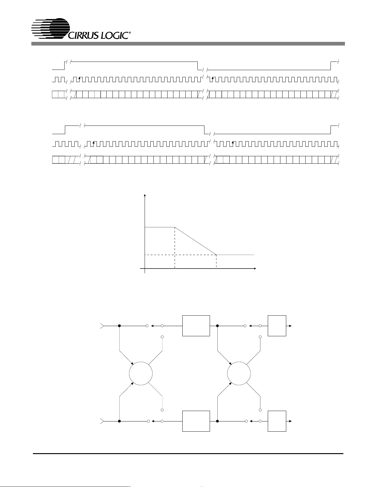
T1=50 µs
0dB
Left Channel
Audio Data
Right Channel
Audio Data
T2 = 15 µs
-10dB
F1 F2
Frequency
3.183 kHz 10.61 kHz
Figure 13. De-Emphasis Curve
A Channel
Volume
Control
MUTE
Aout A
ΣΣ
B Channel
Volume
Control
MUTE
Aout B
Figure 14. ATAPI Block Diagram
32 DS600PP3
Page 33

CS4391A
7. APPLICATIONS
7.1 Recommended Power-up Sequence for Hardware Mode
1) Hold RST low until the power supplies, master,
and left/right clocks are stable.
2) Bring RST high.
7.2 Recommended Power-up Sequence and Access to Control Port Mode
1) Hold RST low until the power supply, master,
and left/right clocks are stable. In this state, the
control port is reset to its default settings and
CMOUT will remain low.
2) Bring RST high. The device will remain in a
low power state with CMOUT low and the control port is accessible.
3) Write 30h to register 5 within 10 ms cycles fol-
lowing the release of RST
.
4) The desired register settings can be loaded
while keeping the PDN bit set to 1.
5) Set the PDN bit to 0 which will initiate the power-up sequence which requires approximately
10 µS.
7.3 Analog Output and Filtering
The application note “Design Notes for a 2-Pole
Filter with Differential Inp ut ” discusses the se condorder
Butterworth filter and differential to singleended converter which was implemented on the
CS4391A evaluation board, CDB4391A. The
CS4391A filter, as seen in Figure 14, is a linear
phase design and does not include phase or amplitude compensation for an external filter. Therefore,
the DAC system phase and amplitude response will
be dependent on the external analog circuitry.
AOUTA-
AOUTA+
C42
C43
10UF
10UF
AMUTEC
R24
R26
R28
5.62K
5.62K
1
GND
GND
GND
C7
2700PF
COG
C14
2700PF
COG
3
2
R17
R18
R15
5.62K
GND
Q4
MMUN2211LT1
1.18K
1.18K
GND
1
2
3
C5
560PF
COG
VA+3/+5
5.62K
C6
560PF
COG
VCC
8
V+
U11
-
+
MC33078D
V-
4
VEE
2
MMUN2111LT1
Q3
3
.1UF
GND
1
C48
.1UF
GND
R25
Figure 15. CS4391A Output Filter
C49
J3
R20
560
HDR8
12
HDR1X2
Q1
2SC2878
2K
2
3
1
GND
R5
47K
CON_RCA_RA
1
2
GNDGND
3
4
AOUTA
NC
DS600PP3 33
Page 34

CS4391A
8. CONTROL PORT INTERFACE
The control port is used to load all the internal settings of the CS4391A. The operation of the control
port may be completely asynchronous to the audio
sample rate. However, to avoid potential interference problems, the control port pins should remain
static if no operation is required.
The control port has 2 modes: SPI and I2C, with the
CS4391A operating as a slave device in both
modes. If I2C operation is desired, AD0/CS should
be tied to VA or AGND. If the CS4391A ever detects a high to low transition on AD0/CS after power-up, SPI mode will be selected. The control port
registers are write-only in SPI mode.
8.1 SPI Mode
In SPI mode, CS is the CS4391A chip select signal,
CCLK is the control port bit cloc k, C DIN is the input data line from the microcontroller and the chip
address is 0010000. All signals are inputs and data
is clocked in on the rising edge of CCLK.
Figure 16 shows the operation of the control por t in
SPI mode. To write to a register, bring CS low. The
first 7 bits on CDIN form the chip address, and
must be 0010000. The eighth bit is a read/write indicator (R/W), which must be low to write. The
next 8 bits form the Memory Address Pointer
(MAP), which is set to the address of the r egister
that is to be updated. The next 8 bits are the data
which will be placed into the register designated by
the MAP. See Table 16.
The CS4391A has MAP auto increment capability,
enabled by the INCR bit in the MAP register. If
INCR is 0, then the MAP will stay constant for successive writes. If INCR is set to 1, then MAP will
auto increment after each byte is written, allowi ng
block reads or writes of successive registers.
8.2 I2C Mode
In I2C mode, SDA is a bi-directional da ta line. Data
is clocked into and out of the part by the clock,
SCL, with the clock to data relationship as shown
in Figure 3. There is no CS pin. Pin AD0 forms the
partial chip address and should be tied to VA or
AGND as required. The upper 6 bits of the 7-bit address field must be 001000. To communicate with
the CS4391A the LSB of the chip address field,
which is the first byte sent to the CS4391A, should
match the setting of the AD0 pin. The eighth bit of
the address byte is the R/W bit (high for a read, low
for a write). If the operation is a write, the next byte
is the Memory Address Pointer, MAP, which selects the register to be read or written. The MAP is
then followed by the data to be written. If the operation is a read, the n the contents of the register
pointed to by the MAP will be output after the chip
address.
The CS4391A has MAP auto increment capability,
enabled by the INCR bit in the MAP register. If
INCR is 0, then the MAP will stay constant for successive writes. If INCR is set to 1, then MAP will
auto increment after each byte is written, allowi ng
block reads or writes of successive registers.
For more information on I2C, please see “The I2CBus Specification: Version 2.0”, listed in the References section.
34 DS600PP3
Page 35

CS4391A
76543210
INCR Reserved Reserved Reserved Reserved MAP2 MAP1 MAP0
00000000
INCR (Auto MAP Increment Enable)
Default = ‘0’.
0 - Disabled
1 - Enabled
MAP0-2 (Memory Address Pointer)
Default = ‘000’.
Table 16. Memory Address Poin ter ( M A P )
CS
CCLK
CDIN
CHIP
ADDRESS
0010000
R/W
MAP
MSB
byte 1
DATA
LSB
byte n
MAP = Memory Address Pointer
Figure 16. Control Port Timing, SPI mode
N ote 1
SDA
SCL
Note : If operation is a w rite, this byte co ntain s the Mem ory A ddre ss P ointer, M A P .
001000
Start
ADDR
AD0
R/W
ACK
DATA
1-8
ACK
DATA
1-8
ACK
Figure 17. Control Port Timing, I2C Mode
Stop
DS600PP3 35
Page 36

CS4391A
A
li
d
dB
0.25
0.2
0.15
0.1
0.05
e
0
tu
-0.05
mp
-0.1
-0.15
-0.2
-0.25
0 0.05 0.1 0.15 0.2 0.25 0.3 0.35 0.4 0.45 0.5
Frequency (normalized to Fs)
Figure 18. Single-Speed Frequency Response Figure 19. Single-Speed Transition Band
Figure 20. Single-Speed Transition Band Figure 21. Single-Speed Stopband Rejection
0.25
0.2
0.15
0.1
0.05
0
-0.05
Amplitude dB
-0.1
-0.15
-0.2
-0.25
0 0.05 0.1 0.15 0. 2 0.25 0.3 0.35 0.4 0.45 0.5
Frequency (normalized to Fs)
Figure 22. Double-Speed Frequency Response Figure 23. Double-Speed Transition Band
36 DS600PP3
Page 37

CS4391A
Figure 24. Double-Speed Transition Band Figure 25. Double-Speed Stopband Rejection
DS600PP3 37
Page 38

9. PARAMETER DEFINITIONS
Total Harmonic Distortion + Noise (THD+N)
The ratio of the rms value of the signal to the rms sum of all other spectral components over the specified
bandwidth (typically 10Hz to 20kHz), including distortion components. Expressed in decibels.
Dynamic Range
The ratio of the full scale rms value of the signal to the rms sum of all other spectral components over the
specified bandwidth. Dynamic range is a signal-to-noise measurement over the specified bandwidth
made with a -60 dBFS signal. 60 dB is then added to the resulting measurement to refer the measurement
to full scale. This technique ensures that the distortion components are below the noise level and do not
effect the measurement. This measurement technique has been accepted by the Audio Engineering Society, AES17-1991, and the Electronic Industries Association of Japan, EIAJ CP-307.
Interchannel Isolation
A measure of crosstalk between the left and right channels. Measured for each channel at the converter's
output with all zeros to the input under test and a full-scale signal applied to the other channel. Units in
decibels.
Interchannel Gain Mismatch
The gain difference between left and right channels. Units in decibels.
CS4391A
Gain Error
The deviation from the nominal full scale analog output for a full scale digital input.
Gain Drift
The change in gain value with temperature. Units in ppm/°C.
10.REFERENCES
1. "How to Achieve Optimum Performance from Delta-Sigma A/D & D/A Converters" by Steven Harris.
Paper presented at the 93rd Convention of the Audio Engineering Society, October 1992.
2. CDB4391A Evaluation Board Datasheet
3. “The I
2
http://www.semiconductors.philips.com
C-Bus Specification: Version 2.0” Philips Semiconductors, December 1998.
38 DS600PP3
Page 39
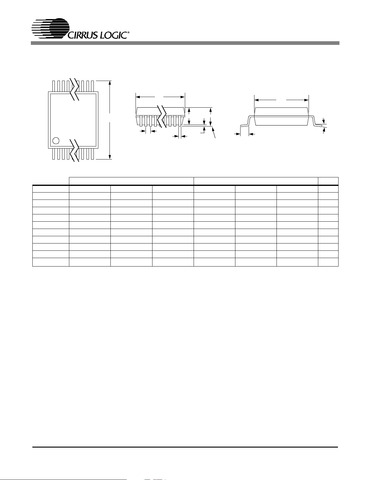
11.PACKAGE DIMENSIONS
20L TSSOP (4.4 mm BODY) PACKAGE DRAWING
N
CS4391A
1
23
TOP VIEW
D
E
e
2
b
SIDE VIEW
A2
A1
A
SEATING
PLANE
L
INCHES MILLIMETERS
1
E1
END VIEW
NOTE
DIM MIN NOM MAX MIN NOM MAX
A -- -- 0.043 -- -- 1.10
A1 0.002 0.004 0.006 0.05 -- 0.15
A2 0.03346 0.0354 0.037 0.85 0.90 0.95
b 0.00748 0.0096 0.012 0.19 0.245 0.30 2,3
D 0.252 0.256 0.259 6.40 6.50 6.60 1
E 0.248 0.2519 0.256 6.30 6.40 6.50
E1 0.169 0.1732 0.177 4.30 4.40 4.50 1
e -- -- 0.026 -- -- 0.65
L 0.020 0.024 0.028 0.50 0.60 0.70
∝
0° 4° 8° 0° 4° 8°
∝
JEDEC #: MO-153
Controlling Dimension is Millimeters.
Notes: 1. “D” and “E1” are reference datums and do not included mold flash or protrusions, but do include mold
mismatch and are measured at the parting line, mold flash or protrusions shall not exceed 0.20 mm per
side.
2. Dimension “b” does not include dambar protrusion/intrusion. Allowable dambar protrusion shall be
0.13 mm total in excess of “b” dimension at maximum material condition. Dambar intrusion shall not
reduce dimension “b” by more than 0.07 mm at least material condition.
3. These dimensions apply to the flat section of the lead between 0.10 and 0.25 mm from lead tips.
DS600PP3 39
Page 40

PACKAGE DIMENSIONS(cont.).
20L SOIC (300 MIL BODY) PACKAGE DRAWING
1
b
CS4391A
HE
c
D
SEATING
PLANE
A
e
A1
L
INCHES MILLIMETERS
DIM MIN NOM MAX MIN NOM MAX
A 0.093 0.098 0.104 2.35 2.50 2.65
A1 0.004 0.008 0.012 0.10 0.20 0.30
b 0.013 0.017 0.020 0.33 0.43 0.51
C 0.009 0.011 0.013 0.23 0.28 0.32
D 0.496 0.504 0.512 12.60 12.80 13.00
E 0.291 0.295 0.299 7.40 7.50 7.60
e 0.040 0.050 0.060 1.02 1.27 1.52
H 0.394 0.407 0.419 10.00 10.34 10.65
L 0.016 0.025 0.050 0.40 0.64 1.27
∝ 0° 4° 8° 0° 4° 8°
JEDEC #: MS-013
Controlling Dimension is Millimeters
∝
40 DS600PP3
 Loading...