

CS4341
24-Bit, 96 kHz Stereo DAC with Volume Control
Features
l Complete Stereo DAC System: Inte rpolation,
D/A, Output Analog Filtering
l ATAPI Mixing
l 101 dB Dynamic Range
l 89 dBFS THD+N
l Low Clock Jitter Sensitivity
l +3 V to +5 V Power Supply
l Filtered Line Level Outputs
l On-Chip Digital De-emphasis for 32, 44.1,
and 48 kHz
l Digital Volume Control with Soft Ramp
– 94 dB Attenuation
– 1 dB Step Size
– Zero Crossing Click-Free Transitions
l 30 mW with 3 V supply
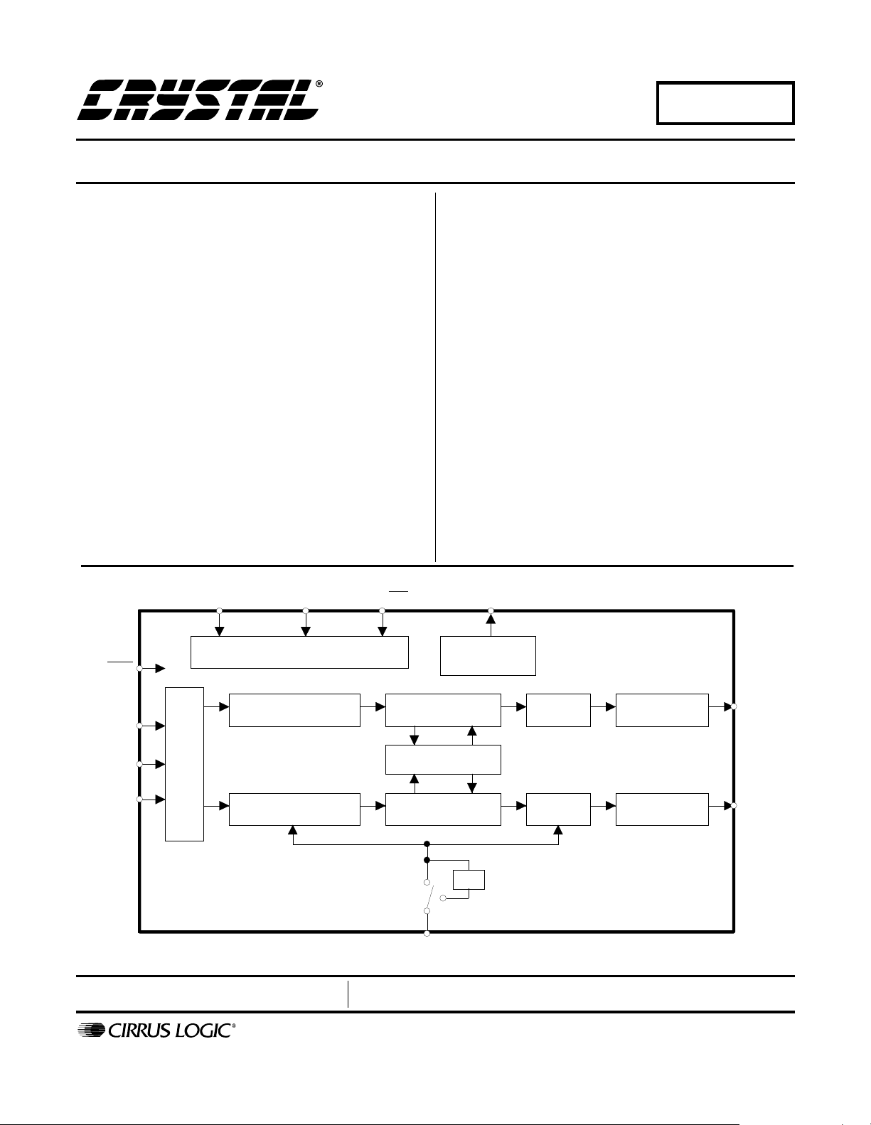
I
SCL/CCLK MUTECAD0/CS
SDA/CDIN
Description
The CS4341 is a comp lete stereo dig ital-to-anal og system including digital interpolation, fourth-order deltasigma digital-to-ana log c onv ers ion , digi tal de -e mph asis ,
volume control, channel mixing and analog filtering. The
advantages of this arc hit ectur e i nclud e: id eal di ffer ent ial
linearity, no distortion mechanisms due to resistor
matching errors, no linearity drift over time and temperature and a high tolerance to clock jitter.
The CS4341 accepts data at audi o sample rates from
2 kHz to 100 kHz, consumes very little power and operates over a wide power supply range. These features are
ideal for DVD, A/V receiver and set-top box systems.
ORDERING INFORMATION
CS4341-KS 16-pin SOIC, -10 to 70 °C
CDB4341 Evaluation Board
Control Port
RST
SCLK
LRCK
SDATA
Serial Port
Preliminary Product Information
P.O. Box 17847, Austin, Texas 78760
(512) 445 7222 FAX: (512) 445 7581
http://www.cirrus.com
External
Mute Control
Volume ControlInterpolation Filter Analog Filter
Mixer
Volume ControlInterpolation Filter
÷2
MCLK
This document contains information for a new product.
Cirrus Logic reserves the right to modify this product without notice.
Copyright Cirrus Logic, Inc. 1999
(All Rights Reserved)
∆Σ
∆Σ
DAC
DAC
Analog Filter
DS298PP2
AOUTA
AOUTB
AUG ‘99
1

TABLE OF CONTENTS
1. CHARACTERISTICS AND SPECIFICATIONS .................................. ....... ...... ....... ...... ....... ..... 5
ANALOG CHARACTERISTICS................................................................................................ 5
POWER AND THERMAL CHARACTERISTICS . ....... ...... ...... ....... ...... ....... ...... ....... ...... ....... ..... 7
DIGITAL CHARACTERISTICS................................................................................................. 7
ABSOLUTE MAXIMUM RATINGS ...........................................................................................7
RECOMMENDED OPERATING CONDITIONS.......................................................................7
SWITCHING CHARACTERISTICS .............. ...... ....... ...... ...... ....... ...... ....... ...... ....... ...... ....... ..... 8
SWITCHING CHARACTERISTICS - CONTROL PORT.........................................................10
2. TYPICAL CONNECTION DIAGRAM ....................................................................................12
3. REGISTER QUICK REFERENCE .......................................................................................... 13
3.1 MCLK Control (address 00h)............................................................................................13
3.2 Mode Control (address 01h)............................................................................................. 13
3.3 Volume and Mixing Control (address 02h)........................................................................ 14
3.4 Channel A Volume Control (address 03h) ........................................................................ 14
3.5 Channel B Volume Control (address 04h) ........................................................................ 14
4. REGISTER BIT DESCRIPTION .............................................................................................. 15
4.1 Master Clock Divide Enable..............................................................................................15
4.2 Auto-Mute .........................................................................................................................15
4.3 Digital Interface Format..................................................................................................... 16
4.4 De-emphasis Control ........................................................................................................16
4.5 Power On/Off Quiescent Voltage Ramp ........................................................................... 17
4.6 Power Down......................................................................................................................17
4.7 Channel A Volume = Channel B Volume.......................................................................... 18
4.8 Soft Ramp or Zero Cross Enable......................................................................................18
4.9 ATAPI Channel Mixing and Muting...................................................................................19
4.10 Mute................................................................................................................................20
4.11 Volume Control ............................................................................................................... 21
CS4341
5. PIN DESCRIPTION ................................ ....... ...... ....... ............................................. ................ 22
Analog Power - VA.................................................................................................................. 22
Analog Ground - AGND ..........................................................................................................22
Contacting Cirrus Logic Support
For a complete listing of Direct Sales, Distributor, and Sales Representative contacts, visit the Cirrus Logic web site at:
http://www.cirrus.com/corporate/contacts/
I2C is a registered trademark of Philips Semiconductors.
Preliminary product info rmation describes products which are i n production, but for whi ch f ull characterization data is not yet available. Advance produ ct i nfor mation describes products which are in development and subject to development changes. Cirrus Logic, Inc. has made best efforts to ensure that the information
contained in this document is accurate and reli able. However , the i nformati on is sub ject to change with out no tice and i s provi ded “AS IS” withou t warranty of
any kind (express or implied). No responsibility is assumed by Cirrus Logic, Inc. for the use of this information, nor for infringements of patents or other rights
of third parties. This document i s the propert y of Cirru s Logic, Inc. and implie s no licen se under patent s, copyri ghts, trademarks, or tr ade secrets. No part of
this publication may be copied, reproduced , stored in a retrieval system, or transmitted, in any form or by any means (electronic, mechanical, photographic, or
otherwise) without the pri or wri tt en consen t of Ci rrus Logic, Inc. Items from any Cirrus Logi c websi te or disk may be printed for use by the user. However, no
part of the printout or electronic files may be copied, reproduced, stored in a retrieval system, or transmitted, in any form or by any means (electronic, mechanical,
photographic, or otherwise) without the prior written consent of Cirrus Logic, Inc.Furthermore, no part of this publication may be used as a basis for manufacture
or sale of any items without the prior written consent of Cirrus Logic, Inc. The names of products of Cirrus Logic, Inc. or other vendors and suppliers appearing
in this document may be trademarks or service marks of their respective owners which may be registered in some jurisdictions. A list of Cirrus Logic, Inc. trademarks and service marks can be found at http://www.cirrus.com.
2 DS298PP2

CS4341
Analog Output - AOUTA and AOUTB..................................................................................... 22
Reference Ground - REF_GND.............................................................................................. 22
Positive Voltage Reference - FILT+ . ...... ....... ...... ....... ...... ...... ....... ....................................... ... 22
Quiescent Voltage - VQ..........................................................................................................22
Master Clock - MCLK .............................................................................................................23
Left/Right Clock - LRCK .........................................................................................................23
Serial Audio Data - SDATA .................................................................................................... 23
Serial Clock - SCLK................................................................................................................ 24
Reset - RST............................................................................................................................ 24
Serial Control Interface Clock - SCL/CCLK........................................................................... 24
Serial Control Data I/O - SDA/CDIN....................................................................................... 24
Address Bit / Chip Select - AD0/CS
Mute Control - MUTEC........................................................................................................... 24
6. APPLICATIONS ..................................................................................................................... 25
6.1 Grounding and Power Supply Decoupling ....................................................................... 25
6.2 Oversampling Modes ....................................................................................................... 25
6.3 Recommended Power-up Sequence ............................................................................... 25
6.4 Use of the Power ON/OFF Quiescent Voltage Ramp ..................................................... 25
7. CONTROL PORT INTERFACE ....... ...... ....... ...... ....... ...... ............................................. ....... ... 26
7.1 SPI Mode ......................................................................................................................... 26
2
7.2 I
C Compatible Mode ...................................................................................................... 26
7.2 Memory Address Pointer (MAP)....................................................................................... 27
........................................................................................ 24
8. PARAMETER DEFINITIONS .................................................................................................. 33
Total Harmonic Distortion + Noise (THD+N) .......................................................................... 33
Dynamic Range...................................................................................................................... 33
Interchannel Isolation ............................................................................................................. 33
Interchannel Gain Mismatch................................................................................................... 33
Gain Error............................................................................................................................... 33
Gain Drift ................................................................................................................................ 33
9. REFERENCES .......................... ....... ...... ....... ...... ....... ...... ...... ....... ...... ....... ............................. 33
10. PACKAGE DIMENSIONS .................................................................................................... 34
LIST OF FIGURES
Figure 1. External Serial Mode Input Timing ................................................................................. 9
Figure 2. Internal Serial Mode Input Timing .................................................................................. 9
Figure 3. Internal Serial Clock Generation .................................................................................... 9
Figure 4. I
Figure 5. SPI Control Port Timing ...............................................................................................11
Figure 6. Typical Connection Diagram ........................................................................................ 12
Figure 7. SPI Mode Control Port Formating ................................................................................ 27
Figure 8. I
Figure 9. Base-Rate Stopband Rejection .................................................................................... 28
Figure 10. Base-Rate Transition Band .......................................................................................... 28
Figure 11. Base-Rate Transition Band (Detail) ............................................................................. 28
Figure 12. Base-Rate Passband Ripple ........................................................................................ 28
Figure 13. High-Rate Stopband Rejection .................................................................................... 28
Figure 14. High-Rate Transition Band ........................................................................................... 28
Figure 15. High-Rate Transition Band (Detail) .............................................................................. 29
Figure 16. High-Rate Passband Ripple ......................................................................................... 29
Figure 17. Output Test Load ......................................................................................................... 29
2
C Control Port Timing ................................................................................................ 10
2
C Mode Control Port Formating ................................................................................ 27
DS298PP2 3

Figure 18. Maximum Loading ........................................................................................................29
Figure 19. Power vs. Sample Rate (VA = 5V) ............................................................................... 29
Figure 20. CS4341 Format 0 (I
Figure 21. CS4341 Format 1 (I
Figure 22. CS4341 Format 2 .........................................................................................................30
Figure 23. CS4341 Format 3 .........................................................................................................31
Figure 24. CS4341 Format 4 .........................................................................................................31
Figure 25. CS4341 Format 5 .........................................................................................................31
Figure 26. CS4341 Format 6 .........................................................................................................32
Figure 27. De-Emphasis Curve .....................................................................................................32
Figure 28. ATAPI Block Diagram ..................................................................................................32
2
S) ................................................................................................ 30
2
S) ................................................................................................ 30
LIST OF TABLES
Table 1. Master Clock Divide Enable ...............................................................................................15
Table 2. Auto-Mute Enable...............................................................................................................15
Table 3. Digital Interface Formats .................................................................................................... 16
Table 4. De-emphasis Filter Configurations .....................................................................................16
Table 5. Power On/Off Ramp Enable...............................................................................................17
Table 6. Power Down Enable........................................................................................................... 17
Table 7. A=B Volume Control Enable...............................................................................................18
Table 8. Soft Ramp and Zero Cross Enable.....................................................................................19
Table 9. ATAPI Decode.................................................................................................................... 19
Table 10. Mute Enable ..................................................................................................................... 20
Table 11. Digital Volume Settings .................................................................................................... 21
Table 12. Common Clock Frequencies ............................................................................................23
CS4341
4 DS298PP2
1. CHARACTERISTICS AND SPECIFICATIONS
CS4341
ANALOG CHARACTERISTICS (T
Full-Scale Output Sine Wave, 997 Hz; MCLK = 12.288 MHz; Fs for Base-rate Mode = 48 kHz, SCLK = 3.072 MHz,
Measurement Bandwidth 10 Hz to 20 kHz, unless otherwise specified; Fs for High-Rate Mode = 96 kHz,
SCLK = 6.144 MHz, Measurement Bandwidth 10 Hz to 40 kHz, unless otherwise specified. Test load R
C
= 10 pF (see Figure 17)),
L
Parameter
= 25 °C; Logic "1" = VA = 5 V; Logic "0" = AGND;
A
= 10 k
L
Base-rate Mode High-Rate Mode
Symbol Min T yp Max Min Typ Max Unit
Ω,
Dynamic Performance for VA = 5 V
Specified Temperature Range T
Dynamic Range (Note 1)
18 to 24-Bit
unweighted
A-Weighted
16-Bit unweighted
A-Weighted
Total Harmonic Distortion + Noise (Note 1)
18 to 24-Bit 0 dB
-20 dB
-60 dB
16-Bit 0 dB
-20 dB
-60 dB
Interchannel Isolation (1 kHz) - 100 - - 100 - dB
A
THD+N
-10 - 70 -10 - 70 °C
dB
92
96
91
97
101
-
-
-
-
-
-
-
-
95
99
-89
-77
-37
-88
-75
-35
-
-
-
-
-84
-72
-32
-
-
-
95
-
-
-
-
-
-
-
-
96
100
94
98
-89
-74
-36
-89
-73
-34
-
-
-
-
-84
-69
-31
-
-
-
dB
dB
dB
dB
dB
dB
dB
dB
dB
Dynamic Performance for VA = 3 V
Specified Temperature Range T
Dynamic Range (Note 1)
18 to 24-Bit
unweighted
A-Weighted
16-Bit unweighted
A-Weighted
Total Harmonic Distortion + Noise (Note 1)
18 to 24-Bit 0 dB
-20 dB
-60 dB
16-Bit 0 dB
-20 dB
-60 dB
Interchannel Isolation (1 kHz) - 100 - - 100 - dB
A
THD+N
-10 - 70 -10 - 70 °C
dB
99
102
-
-
-
-
-
-
-
-
94
97
93
96
-94
-74
-34
-93
-73
-33
-
-
-
-
-89
-69
-29
-
-
-
97
101
-
-
-
-
-
-
-
-
92
96
91
96
-92
-76
-32
-91
-71
-31
-
-
-
-
-87
-71
-27
-
-
-
dB
dB
dB
dB
dB
dB
dB
dB
dB
Notes: 1. One-half LSB of triangular PDF dither is added to data.
DS298PP2 5
CS4341
ANALOG CHARACTERISTICS (Continued)
Parameters Symbol Min Typ Max Units
Analog Output
Full Scale Output Voltage 0.63•VA 0.7•VA 0.77•VA Vpp
Quiescent Voltage V
Interchannel Gain Mismatch - 0.1 - dB
Gain Drift - 100 - ppm/°C
AC-Load Resistance (Note 2) R
Load Capacitance (Note 2) C
Parameter
Symbol Min T yp Max Min Typ Max Unit
Q
L
L
Base-rate Mode High-Rate Mode
Combined Digital and On-chip Analog Filter Response (Note 3)
Passband (Note 4)
to -0.05 dB corner
to -0.1 dB corner
to -3 dB corner
Frequency Response 10 Hz to 20 kHz -.02 - +.08 -0.06 - 0 dB
StopBand .5465 - - .577 - - Fs
StopBand Attenuation (Note 5) 50 - - 55 - - dB
Group Delay tgd - 9/Fs - - 4/Fs - s
Passband Group Delay Deviation 0 - 40 kHz
0 - 20 kHz
De-emphasis Error Fs = 32 kHz
(Relative to 1 kHz) Fs = 44.1 kHz
Fs = 48 kHz
0
-
0
-
--±0.36/Fs
-
-
-
-
-
-
-
-
-
-0.5•VA- VDC
3--k
--100pF
.4535
-
.4998
-
-
+.2/-.1
+.05/-.14
+0/-.22
0
0
--±1.39/Fs
-
-
-
±0.23/Fs--
(Note 6)
.4621
.4982
Ω
-
dB
dB
dB
Fs
Fs
Fs
s
s
Notes: 2. Refer to Figure 18.
3. Filter response is guarant e ed by de sign.
4. Response is clock dependent and will scale with Fs. Note that the response plots (Figures 9-16) have
been normalized to Fs and can be de-normalized by multiplying the X-axis scale by Fs.
5. For Base-Rate Mode, the Measurement Bandwidth is 0.5465 Fs to 3 Fs.
For High-Rate Mode, the Measurement Bandwidth is 0.577 Fs to 1.4 Fs.
6. De-em phasis is not available in High-Rate Mod e.
6 DS298PP2
POWER AND THERMAL CHARACTERISTICS
Parameters Symbol Min Typ Max Units
Power Supplies
Power Supply Current normal operation
VA = 5 V power-down state
Power Dissipation (Note 7)
VA = 5 V normal operation
power-down
Power Supply Current normal operation
VA = 3 V power-down state
Power Dissipation (Note 7)
VA = 3 V normal operation
power-down
Package Thermal Resistance
Power Supply Rejection Ratio (1 kHz) (Note 8)
(60 Hz)
Notes: 7. Refer to Figure 19.
8. Valid with the recommended capacitor values on FILT+ and V
I
A
I
A
I
A
I
A
θ
JA
PSRR -
CS4341
-
-
-
-
-
-
-
-
-110-°C/Watt
-
as shown in Figure 1.
Q
15
60
75
0.3
10
30
30
0.09
60
40
17
85
14
42
mA
-
µ
A
mW
-
mW
mA
-
µ
A
mW
-
-
-
mW
dB
dB
DIGITAL CHARACTERISTICS (T
= 25°C; VA = 2.7V - 5.5V)
A
Parameters Symbol Min Typ Max Units
High-Level Input Voltage VA = 5 V
VA = 3 V
Low-Level Input Voltage VA = 5 V
VA = 3 V
Input Leakage Current I
V
IH
V
IL
in
2.0
2.0
-
-
-
-
-
-
-
-
0.8
0.8
--±10µA
V
V
V
V
Input Capacitance - 8 - pF
Maximum MUTEC Drive Current - 3 - mA
ABSOLUTE MAXIMUM RATINGS (AGND = 0V; all voltages with respect to ground.)
Parameters Symbol Min Max Units
DC Power Supply VA -0.3 6.0 V
Input Current, Any Pin Except Supplies I
Digital Input Voltage V
Ambient Operating Temperature (power applied) T
Storage Temperature T
in
IND
A
stg
-±10mA
-0.3 VA+0.4 V
-55 125 °C
-65 150 °C
WARNING: Operation at or beyond these limits may result in permanent damage to the device. Normal operation is
not guaranteed at these extremes.
RECOMMENDED OPERATING CONDITIONS (AGND = 0V; all voltages with respect to ground.)
Parameters Symbol Min Typ Max Units
DC Power Supply VA 2.7 5.0 5.5 V
DS298PP2 7
CS4341
1
1
1
SWITCHING CHARACTERISTICS (T
Logic 1 = VA, C
= 20pF)
L
= -10 to 70°C; VA = 2.7V - 5.5V; Inputs: Logic 0 = 0V,
A
Parameters Symbol Min Typ Max Units
Input Sample Rate Fs 2 - 100 kHz
MCLK Pulse Width High MCLK/LRCK = 512 10 - 1000 ns
MCLK Pulse Width Low MCLK/LRCK = 512 10 - 1000 ns
MCLK Pulse Width High MCLK / LRCK = 384 or 192 21 - 1000 ns
MCLK Pulse Width Low MCLK / LRCK = 384 or 192 21 - 1000 ns
MCLK Pulse Width High MCLK / LRCK = 256 or 128 31 - 1000 ns
MCLK Pulse Width Low MCLK / LRCK = 256 or 128 31 - 1000 ns
External SCLK Mode
LRCK Duty Cycle (External SCLK only) 40 50 60 %
SCLK Pulse Width Low t
SCLK Pulse Width High t
SCLK Period MCLK / LRCK = 512, 256 or 384 t
SCLK Period MCLK / LRCK = 128 or 192 t
SCLK rising to LRCK edge delay t
SCLK rising to LRCK edge setup time t
SDATA valid to SCLK rising setup time t
SCLK rising to SDATA hold time t
sclkl
sclkh
sclkw
sclkw
slrd
slrs
sdlrs
sdh
20 - - ns
20 - - ns
1
---------------------128()Fs
1
-----------------64()Fs
--ns
--ns
20 - - ns
20 - - ns
20 - - ns
20 - - ns
Internal SCLK Mode
LRCK Duty Cycle (Internal SCLK only) (Note 9) - 50 - %
SCLK Period (Note 10) t
SCLK rising to LRCK edge t
SDATA valid to SCLK rising setup time t
SCLK rising to SDATA hold time
MCLK / LRCK = 512, 256 or 128
SCLK rising to SDATA hold time
MCLK / LRCK = 384 or 192
sclkw
sclkr
sdlrs
t
sdh
t
sdh
---------------SCLK
--
----------------------10+
512()Fs
1
----------------------15+
512()Fs
----------------------15+
384()Fs
--ns
tsclkw
----------------- 2
µ
--ns
--ns
--ns
s
Notes: 9. In Internal SCLK Mode, the Duty Cycle must be 50% ±1/2 MCLK Period.
10. The SCLK / LRCK ratio may be either 32, 48, or 64. This ratio depends on part type and MCLK/LRCK
ratio. (See Figures 20-26)
8 DS298PP2
LRCK
SCLK
t
slrd
t
slrs
t
sclkl
t
sclkh
CS4341
SDATA
LRCK
SDATA
*INTERNAL SCLK
*The SCLK pulses shown are internal to the CS4341.
t
sdlrs
t
sdh
Figure 1. External Serial Mode Input Timing
t
sclkr
t
sclkw
t
sdlrstsdh
Figure 2. Internal Serial Mode Input Timing
LRCK
MCLK
*INTERNAL SCLK
SDATA
1
N
2
N
Figure 3. Internal Serial Clock Generation
* The SCLK pulses shown are internal to the CS4341.
N equals MCLK divided by SCLK
DS298PP2 9
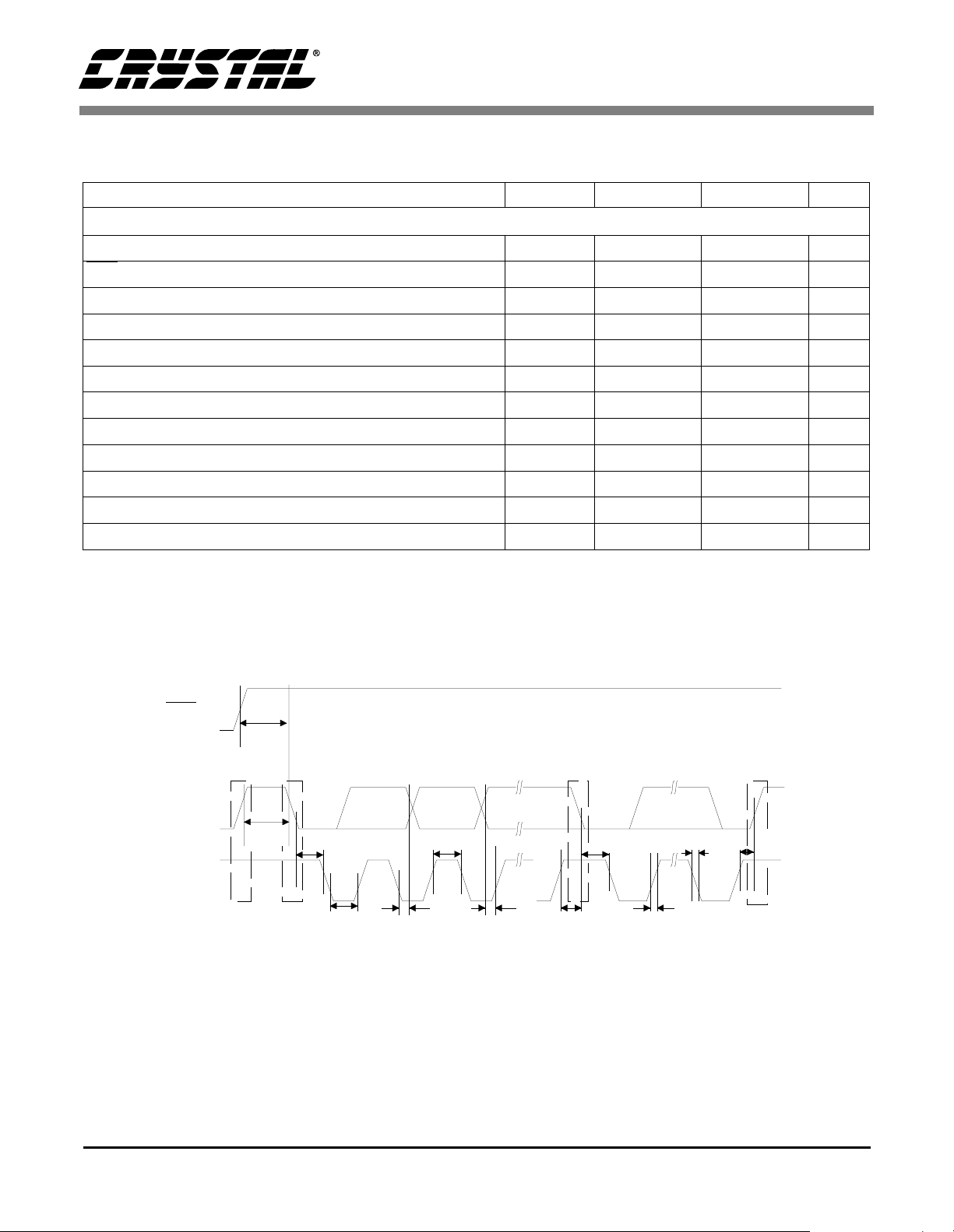
SWITCHING CHARACTERISTICS - CONTROL PORT
(TA = 25 °C; VA = +5 V ±5%; Inputs: logic 0 = AGND, logic 1 = VA, CL = 30 pF)
Parameter Symbol Min Max Unit
I2C® Compatible Mode
SCL Clock Frequency f
Rising Edge to Start t
RST
Bus Free Time Between Transmissions t
Start Condition Hold Time (prior to first clock pulse) t
Clock Low time t
Clock High Time t
Setup Time for Repeated Start Condition t
SDA Hold Time from SCL Falling (Note 11) t
SDA Setup time to SCL Rising t
Rise Time of Both SDA and SCL Lines t
Fall Time of Both SDA and SCL Lines t
Setup Time for Stop Condition t
scl
irs
buf
hdst
low
high
sust
hdd
sud
r
f
susp
CS4341
-100kHz
500 - ns
4.7 - µs
4.0 - µs
4.7 - µs
4.0 - µs
4.7 - µs
0-µs
250 - ns
-1µs
-300ns
4.7 - µs
Notes: 11. Data must be held for sufficient time to bridge the 300 ns transition time of SCL.
RST
t
SDA
SCL
irs
Stop Start
t
buf
t
t
hdst
low
t
hdd
t
high
t
sud
Repeated
Start
t
sust
t
hdst
t
f
t
r
Figure 4. I2C Control Port Timing
Stop
t
susp
10 DS298PP2
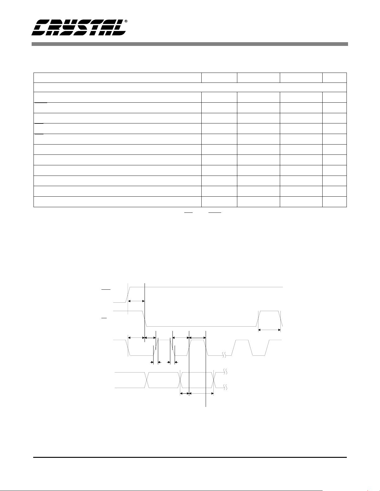
SWITCHING CHARACTERISTICS - CONTROL PORT
(TA = 25 °C; VA = +5 V ±5%; Inputs: logic 0 = AGND, logic 1 = VA, CL = 30 pF)
Parameter Symbol Min Max Unit
SPI Mode
CCLK Clock Frequency f
RST
Rising Edge to CS Falling t
CCLK Edge to CS
CS
High Time Between Transmissions t
CS
Falling to CCLK Edge t
Falling (Note 12) t
CCLK Low Time t
CCLK High Time t
CDIN to CCLK Rising Setup Time t
CCLK Rising to DATA Hold Time (Note 13) t
Rise Time of CCLK and CDIN (Note 14) t
Fall Time of CCLK and CDIN (Note 14) t
sclk
srs
spi
csh
css
scl
sch
dsu
dh
r2
f2
CS4341
-6MHz
500 - ns
500 - ns
1.0 - µs
20 - ns
66 - ns
66 - ns
40 - ns
15 - ns
-100ns
-100ns
Notes: 12. t
13. Data must be held for sufficient time to bridge the transition time of CCLK.
14. For F
only needed before first falling edge of CS after RST rising edge. t
spi
< 1 MHz
SCK
RST
CS
CCLK
CDIN
t
srs
t
t
css
spi
t
r2
t
t
sch
scl
t
f2
= 0 at all other times.
spi
t
csh
t
t
dsu
dh
Figure 5. SPI Control Port Timing
DS298PP2 11

2. TYPICAL CONNECTION DIAGRAM
CS4341
Audio
Data
Processor
External Clock
µ - Controlled
Configuration
2
3
4
5
6
7
8
1
SDATA
SCLK
LRCK
MCLK
SCL/CCLK
SDA/CDIN
AD0/CS
RST
AGND
14
VA
CS4341
13
0.1 µF
AOUTA
MUTEC
FILT+
VQ
REF_GND
AOUTB
1µF
1µF
+5Vto+3V
Ω
560
0.1 µF
Ω
560
+
C
1µF
C
C=
OPTIONAL
MUTE
CIRCUIT
R560
+
L
π
4
Fs(R
L
560)
Audio
Output A
R
L
Audio
Output B
R
L
+
3.3 µF
15
+
Ω
10 k
16
9
10
.1 µF
+
11
3.3 µF
12
+
Ω
10 k
Figure 6. Typical Connection Diagram
12 DS298PP2

CS4341
3. REGISTER QUICK REFERENCE
** “default” ==> bit status after power-up-sequence or reset.
3.1 MCLK Control (address 00h)
76543210
Reserved Reserved Reserved Reserved Reserved Reserved MCLKDIV Reserved
00000000
MCLKDIV (MCLK Divide-by-2 Enable)
Default = ‘0’.
0 - Disabled
1 - Enabled
3.2 Mode Control (address 01h)
76543210
AMUTE DIF2 DIF1 DIF0 DEM1 D EM0 POR PDN
10000011
AMUTE (Auto-mute)
Default = ‘1’.
0 - Disabled
1 - Enabled
DIF2, DIF1 and DIF0 (Digital Interface Format)
Default = ‘0’.
0 - Format 0, I
1 - Format 1, I
2 - Format 2, Left Justified, up to 24-bit data
3 - Format 3, Right Justified, 24-bit Data
4 - Format 4, Right Justified, 20-bit Data
5 - Format 5, Right Justified, 16-bit Data
6 - Format 6, Right Justified, 18-bit Data
7 - Identical to Format 1
DEM 1, DEM 0 (De-Emphasis Mode)
Default = ‘0’.
0 - Disabled
1 - 44.1 kHz De-Emphasis
2 - 48 kHz De-Emphasis
3 - 32 kHz De-Emphasis
POR (Power on/off Quiescent Voltage ramp)
Default = ‘1’.
0 - Disabled
1 - Enabled
PDN (Power-Down)
Default =’1’.
0 - Disabled
1 - Enabled
2
S, up to 24-bit data, 64 x Fs Internal SCLK
2
S, up to 24-bit data, 32 x Fs Internal SCLK
DS298PP2 13

CS4341
3.3 Volume and Mixing Control (address 02h)
76543210
A = B Soft Zero Cross ATAPI4 ATAPI3 ATAPI2 ATAPI1 ATAPI0
01001001
A = B (Channel A Volume = Channel B Volume)
Default = ‘0’.
0 - AOUTA volume is determined by register 03h and AOUTB volume is determined by register
04h.
1 - AOUTA and AOUTB volumes are determined by register 03h and register 04h is ignored.
Soft & Zero Cross (Soft control and zero cross detection control)
Default = ‘10’.
Soft Zero Cross Mode
0 0 Changes take effect immediately
0 1 Changes take effect on zero crossings
1 0 Changes take effect with a soft ramp (default)
1 1 Changes take effect in 1/8 dB steps on each zero crossing
ATAPI 0-4 (Channel mixing and muting)
(refer to Table 9)
Default = ‘01001’, (Stereo)
AOUTA = Left Channel
AOUTB = Right Channel
3.4 Channel A Volume Control (address 03h)
3.5 Channel B Volume Control (address 04h)
76543210
MUTE VOL6 VOL5 VOL4 VOL3 VOL2 VOL1 VOL0
00000000
MUTE
Default = ‘0’
0 - Disabled
1 - Enabled
Volume
Default = ‘0’
(Refer to Table 11)
14 DS298PP2

CS4341
4. REGISTER BIT DESCRIPTION
4.1 MASTER CLOCK DIVIDE ENABLE
MCLK Control Register (address 00h)
76543210
Reserved Reserved Reserved Reserved Reserved Reserved MCLKDIV Reserved
Access:
R/W in I2C and write only in SPI.
Default:
0 - Disabled
Function:
The MCLKDIV bit enables a circuit which divides the externally applied MCLK signal by 2.
Note: This feature is present on revision C and newer devices. For backward compatibility with previous revision devices, this bit defaults to zero.
MCLKDIV MODE
0 Disabled
1 Enabled
Table 1. Master Clock Divide Enable
4.2 AUTO-MUTE
Mode Control Register (address 01h)
76543210
AMUTE DIF2 DIF1 DIF0 DEM1 DEM0 POR PDN
Access:
R/W in I2C and write only in SPI.
Default:
1 - Enabled
Function:
The Digital-to-Analog converter output will mute following the reception of 8192 consecutive audio
samples of st atic 0 or -1. A single sa mple of non-ze ro data w ill rel ease t he mute. Detect ion an d muting is done independently for each channel. The quiescent voltage on the output will be retained and
the Mute Control pin will go active during the mute period. The muting function is effected, similiar to
volume control changes, by the Soft and Zero Cross bits in the Volume and Mixing Control register.
AMUTE MODE
0 Disabled
1 Enabled
Table 2. Auto-Mute Enable
DS298PP2 15

CS4341
4.3 DIGITAL INTERFACE FORMAT
Mode Control Register (address 01h)
76543210
AMUTE DIF2 DIF1 DIF0 DEM1 D EM0 POR PDN
Access:
R/W in I2C and write only in SPI.
Default:
0 - Format 0 (I2S, up to 24-bit data, 64 x Fs Internal SCLK)
Function:
The required relationship between the Left/Right clock, serial clock and serial data is defined by the
Digital Interface Format and the options are detailed in Figures 20-26.
DIF2 DIF1 DIF0 D ESCRIPTION FORMAT FIGURE
000
001
0 1 0 Left Justified, up to 24-bit data 2 22
0 1 1 Right Justified, 24-bit Data 3 23
1 0 0 Right Justified, 20-bit Data 4 24
1 0 1 Right Justified, 16-bit Data 5 25
1 1 0 Right Justified, 18-bit Data 6 26
1 1 1 Identical to Format 1 7 20
2
S, up to 24-bit data, 64 x Fs Internal SCLK
I
2
I
S, up to 24-bit data, 32 x Fs Internal SCLK
Table 3. Digital Interface Formats
020
121
4.4 DE-EMPHASIS CONTROL
Mode Control Register (address 01h)
76543210
AMUTE DIF2 DIF1 DIF0 DEM1 D EM0 POR PDN
Access:
R/W in I2C and write only in SPI.
Default:
0 - Disabled
Function:
Implementation of the standard 15µs/50µs digital de-emphasis filter response, Figure 27, requires reconfiguration of the digital filter to maintain the proper filter response for 32, 44.1 or 48 kHz sample
rates. NOTE: De-emphasis is not available in High-Rate Mode.
DEM1 DEMO DESCRIPTION
0 0 Disabled
0144.1kHz
1048kHz
1132kHz
Table 4. De-emphasis Filter Configurations
16 DS298PP2

CS4341
4.5 POWER ON/OFF QUIESCENT VOLTAGE RAMP
Mode Control Register (address 01h)
76543210
AMUTE DIF2 DIF1 DIF0 DEM1 D EM0 POR PDN
Access:
R/W in I2C and write only in SPI.
Default:
1 - Enabled
Function:
The power On/Off Quiescent Voltage Ramp allows the quiescent voltage to slowly ramp to and from
0 volts to the quiescent voltage during power-on or power-off. Please refer to the applications section
for details of implementing this feature.
POR MODE
0 Disabled
1 Enabled
Table 5. Power On/Off Ramp Enable
4.6 POWER DOWN
Mode Control Register (address 01h)
76543210
AMUTE DIF2 DIF1 DIF0 DEM1 D EM0 POR PDN
Access:
R/W in I2C and write only in SPI.
Default:
1 - Enabled
Function:
The device will enter a low-power state whenever this function is activated. The power-down bit de-
faults to ‘enabled’ on power-up and must be disabled before normal operation will begin. The contents
of the control registers are retained in this mode.
PDN MODE
0 Disabled
1 Enabled
Table 6. Power Down Enable
DS298PP2 17

CS4341
4.7 CHANNEL A VOLUME = CHANNEL B VOLUME
Volume and Mixing Control Register (address 02h)
76543210
A = B Soft Zero Cross ATAPI4 ATAPI3 ATAPI2 ATAPI1 ATAPI0
Access:
R/W in I2C and write only in SPI.
Default:
0 - Disabled
Function:
The AOUTA and AOUTB volume levels are independently controlled by the A and the B Channel Volume Control Bytes when this function is disabled. The volume on both AOUTA and AOUTB are determined by the A Channel Volume Control Byte and the B Channel Byte is ignored when this function
is enabled.
A = B MODE
0 Disabled
1 Enabled
Table 7. A=B Volume Control Enable
4.8 SOFT RAMP OR ZERO CROSS ENABLE
Volume and Mixing Control Register (address 02h)
76543210
A = B Soft Zero Cross ATAPI4 ATAPI3 ATAPI2 ATAPI1 ATAPI0
Access:
R/W in I2C and write only in SPI.
Default:
10 - Soft Ramp enabled.
Function:
Soft Ramp Enable
Soft Ramp allows level changes, both muting and attenuation, to be implemented by incrementally
ramping, in 1/8 dB steps, from the current level to the new level at a rate of 1dB per 8 left/right clock
periods.
Zero Cross Enable
Zero Cross Enable dictates that signal level changes, either by attenuation changes or muting, will
occur on a signal zero crossing to minimize audible artifacts. The requested level change will occur
after a timeout period between 512 and 1024 sample periods (10.7 ms to 21.3 ms at 48 kHz sample
rate) if the signal does not encounter a zero crossing. The zero cross function is indepently monitored
and implemented for each channel.
18 DS298PP2

CS4341
Soft Ramp and Zero Cross Enable
Soft Ramp and Zero Cross Enable dictates that signal level changes, either by attenuation changes
or muting, will occur in 1/8 dB steps and be implemented on a signal zero crossing. The 1/8 dB level
change will occur after a timeout period between 512 and 1024 sample periods (10.7 ms to 21.3 ms
at 48 kHz sample rate) if the signal does not encounter a zero crossing. The zero cross function is
indepently monitored and implemented for each channel.
SOFT ZERO Mode
0 0 Changes to affect immediately
0 1 Zero Cross enabled
1 0 Soft Ramp enabled
1 1 Soft Ramp and Zero Cross enabled
Table 8. Soft Ramp and Zero Cross Enable
4.9 ATAPI CHANNEL MIXING AND MUTING
Volume and Mixing Control Register (address 02h)
76543210
A = B Soft Zero Cross ATAPI4 ATAPI3 ATAPI2 ATAPI1 ATAPI0
Access:
R/W in I2C and write only in SPI.
Default:
01001 - AOUTA=aL, AOUTB=bR (Stereo)
Function:
The CS4341 implements the channel mixing functions of the ATAPI CD-ROM specification. Refer to
Table 9 and Figure 28 for additional information.
ATAPI4 ATAPI3 ATAPI2 ATAPI1 ATAPI0 AOU TA AOUTB
00000 MUTE MUTE
00001 MUTE bR
00010 MUTE bL
00011 MUTE b[(L+R)/2]
00100 aR MUTE
00101 aR bR
00110 aR bL
00111 aR b[(L+R)/2]
01000 aL MUTE
01001 aL bR
01010 aL bL
01011 aL b[(L+R)/2]
01100 a[(L+R)/2] MUTE
01101 a[(L+R)/2] bR
01110 a[(L+R)/2] bL
01111 a[(L+R)/2] b[(L+R)/2]
10000 MUTE MUTE
10001 MUTE bR
Table 9. ATAPI Decode
DS298PP2 19

ATAPI4 ATAPI3 ATAPI2 ATAPI1 ATAPI0 AOU TA AOUTB
10010 MUTE bL
10011 MUTE [(aL+bR)/2]
10100 aR MUTE
10101 aR bR
10110 aR bL
10111 aR [(bL+aR)/2]
11000 aL MUTE
11001 aL bR
11010 aL bL
11011 aL [(aL+bR)/2]
11100[(aL+bR)/2] MUTE
11101[(aL+bR)/2] bR
11110[(bL+aR)/2] bL
11111[(aL+bR)/2] [(aL+bR)/2]
Table 9. ATAPI Decode (Continued)
4.10 MUTE
Channel A Volume Control Register (address 03h)
CS4341
Channel B Volume Control Register (address 04h)
76543210
MUTE VOL6 VOL5 VOL4 VOL3 VOL2 VOL1 VOL0
Access:
R/W in I2C and write only in SPI.
Default:
0 - Disabled
Function:
The Digital-to-Analog converter output will mute when enabled. The quiescent voltage on the output
will be retained. The muting function is effected, similiar to attenuation changes, by the Soft and Zero
Cross bits in the Volume and Mixing Control register. The MUTEC will go active during the mute period if the Mute function is enabled for both channels.
MUTE MODE
0 Disabled
1 Enabled
Table 10. Mute Enable
20 DS298PP2

CS4341
4.11 VOLUME CONTROL
Channel A Volume Control Register (address 03h)
Channel B Volume Control Register (address 04h)
76543210
MUTE VOL6 VOL5 VOL4 VOL3 VOL2 VOL1 VOL0
Access:
R/W in I2C and write only in SPI.
Default:
0 - 0 dB (No attenuation)
Function:
The digital volume control allows the user to attenuate the signal in 1 dB increments from 0 to -90 dB.
Volume settings are decoded as shown in Table 11. The volume changes are implemented as dictated by the Soft and Zero Cross bits in the Volume and Mixing Control register. All volume settings
less than - 94 dB are equivalent to enabling the Mute bit.
Binary Code Decimal Value Volume Setting
0000000 0 0 dB
0010100 20 -20 dB
0101000 40 -40 dB
0111100 60 -60 dB
1011010 90 -90 dB
Table 11. Digital Volume Settings
DS298PP2 21

5. PIN DESCRIPTION
Reset RST MUTEC Mute Contr ol
CS4341
161
Serial Data SDATA AOUTA Analog Output A
Serial Clock SCLK VA Analog Power
Left/Right Clock LRCK AGND Analog Ground
Master Clock MCLK AOUTB Analog Output B
SCL/CCLK SCL/CCLK REF_GND Reference Ground
SDA/CDIN SDA/CDIN VQ Quiescent Voltage
AD0/CS
Analog Power - VA
Pin 14, Input
Function:
Analog power supply. Typically 3 to 5V DC.
Analog Ground - AGND
Pin 13, Input
Function:
Analog ground refer ence.
Analog Output - AOUTA and AOUTB
Pins 12 and 15, Output
Function:
The full scale analog output level is specified in the Analog Characteristics specifications table.
152
143
134
125
116
107
AD0/CS FILT+ Positive Voltage Reference
98
Reference Ground - REF_GND
Pin 11, Input
Function:
Ground reference for the internal sampling circuits. Must be connected to analog ground.
Positive Voltage Reference - FILT+
Pin 9, Output
Function:
Positive reference for internal sampling circuits. External capacitors are required from FILT+ to analog
ground, as shown in Figure 6. The recommended values will typically provide 60 dB of PSRR at 1 kHz
and 40 dB of PSRR at 60 Hz. FILT+ is not intended to supply external current. FILT+ has a typical source
impedence of 250 kΩ and any current drawn from this pin will alter device performance.
Quiescent Voltage - VQ
Pin 10, Output
Function:
Filter connection for internal quiescent reference voltage, typically 50% of VA. Capacitors must be connected from V
has a typical source impedence of 250 kΩ and any current drawn from this pin will alter device performance.
22 DS298PP2
to analog ground, as shown in Figure 6. VQ is not intended to supply external current. VQ
Q

Master Clock - MCLK
Pin 5, Input
Function:
The master clock frequency must be either 256x, 384x, 512x, 768x or 1024x the input sample rate in Base
Rate Mode (BRM) and 128x, 192x, 256x or 384x the input sample rate in High Rate Mode (HRM). Note
that some multiplication factors require setting the MCLKDIV bit in the MCLK Control Register. Table 12
illustrates several standard audio sample rates and the required master clock frequencies.
MCLK (MHz)
Sample Rate
(kHz)
32 4.0960 6.1440 8.1920 12.2880 8.1920 12.2880 16.3840 24.5760 32.7680
44.1 5.6448 8.4672 11.2896 16.9344 11.2896 16.9344 22.5792 32.7680 45.1584
48 6.1440 9.2160 12.2880 18.4320 12.2880 18.4320 24.5760 36.8640 49.1520
64 8.1920 12.2880 16.3840 24.5760 - - - - -
88.2 11.2896 16.9344 22.5792 33.8688 - - - - 96 12.2880 18.4320 24.5760 36.8640 - - - - -
128x 192x 256x* 384x* 256x 384x 512x 768x* 1024x*
HRM BRM
CS4341
* Requires MCLKDIV bit = 1 in MCLK Control Register (address 00h)
Ta ble 12. Common Clock Frequencies
Left/Right Clock - LRCK
Pin 4, Input
Function:
The Left/Right clock determines which channel is currently being input on the serial audio data input, SDATA. The frequency of the Left/Right clock must be at the input sample rate. Audio samples in Left/Right
sample pairs will be simultaneously output from the digital-to-analog converter whereas Right/Left pairs
will exhibit a one sample period difference. The required relationship between the Left/Right clock, serial
clock and serial data is defined by the Mode Control Byte and the options are detailed in Figures 20-26.
Serial Audio Data - SDATA
Pin 2, Input
Function:
Two’s complement MSB-first serial data is input on this pin. The data is clocked into SDATA via the serial
clock and the channel is determined by the Left/Right clock. The required relationship between the
Left/Right clock, serial clock and serial data is defined by the Mode Control Byte and the options are detailed in Figures 20-26.
DS298PP2 23

Serial Clock - SCLK
Pin 3, Input
Function:
Clocks the individual bits of the serial data into the SDATA pin. The required relationship between the
Left/Right clock, serial clock and serial data is defined by the Mode Control Byte and the options are detailed in Figures 20-26.
The CS4341 supports both internal and external serial clock generation modes. The Internal Serial Clock
Mode eliminates possible clock interference from an external SCLK. Use of the Internal Serial Clock Mode
is always preferred.
Internal Serial Clock Mode
In the Internal Serial Clock Mode, the serial clock is internally derived and synchronous with the master
clock and left/right clock. The SCLK/LRCK frequency ratio is either 32, 48, or 64 depending upon data
format, as shown in Figures 20-26. Operation in this mode is identical to operation with an external serial
clock synchronized with LRCK.
External Serial Clock Mode
The CS4341 will enter the External Serial Clock Mode whenever 16 low to high transitions are detected
on the SCLK pin during any phase of the LRCK period. The device will revert to Internal Serial Clock Mode
if no low to high transitions are detected on the SCLK pin for 2 consecutive periods of LRCK.
Reset - RST
Pin 1, Input
Function:
The device enters a low power mode and all internal registers are reset to the default settings, including
the control port, when low. When high, the control port becomes operational and the PDN bit must be
cleared before normal operation will occur. The control port can not be accessed when reset is low.
CS4341
Serial Control Interface Clock - SCL/CCLK
Pin 6, Input
Function:
Clocks the serial control data into or from SDA/CDIN.
Serial Control Data I/O - SDA/CDIN
Pin 7, Input/Output
Function:
In I2C mode, SDA is a data I/O line. CDIN is the input data line for the control port interface in SPI mode.
Address Bit / Chip Select - AD0/CS
Pin 8, Input
Function:
In I2C mode, AD0 is a chip address bit. CS is used to enable the control port interface in SPI mode. The
device will enter the SPI mode at anytime a high to low transition is detected on this pin. Once the device
has entered the SPI mode, it will remain until either the part is reset or undergoes a power-down cycle.
Mute Control - MUTEC
Pin 16, Output
Function:
The Mute Control pin goes high during power-up initialization, reset, muting, master clock to left/right clock
frequency rati o is inco rrect or power- down. Th is pin is intended to be use d as a co ntrol f or an e xternal mute
circuit to prevent the clicks and pops that can occur in any single supply system. Use of Mute Control is not
mandatory but recomm en ded f or de signs requ iri ng the ab so lute min imum i n ext ra neou s cli cks an d p ops.
24 DS298PP2

CS4341
6. APPLICATIONS
6.1 Grounding and Power Supply Decoupling
As with any high resolution converter, the CS4341
requires careful attention to power supply and
grounding arrangements to optimize performance.
Figure 6 shows the recommended power arrangement with VA connected to a clean supply. Decoupling capacitors should be located as close to the
device package as possible.
6.2 Oversampling Modes
The CS4341 operates in one of two oversampling
modes based on the input sample rate and the state
of the MCLKDIV bit in the MCLK Control Register. Base Rate Mode (BRM) supports input sample
rates up to 50 kHz while High Rate Mode (HRM)
supports input sample rates up to 100 kHz. When
the MCLKDIV bit is cleared, the devices opera te in
BRM when MCLK/LRCK is 256, 384 or 512 and
in HRM when MCLK/LRCK is 128 or 192. When
the MCLKDIV bit is set, the devices operate in
BRM when MCLK/LRCK is 512, 768 or 1024 and
in HRM when MCLK/LRCK is 256 or 384.
6.3 Recommended Power-up Sequence
1. Hold RST low until the power supply, master,
and left/right clocks are stable. In this state, the
control port is reset to its default settings and V
will remain low.
2. Bring RST high. The device will remain in a low
power state with VQ low and the control port accesable. The desired register settings can be loaded
while keeping the PDN bit set to 1.
3. Set the PDN bit to 0 which will initiate the pow-
er-up sequence, which requires approximately 50
µ s when the POR bit is set to 0. If the POR bit is
set to 1, see Section 6.4 for total power-up timing.
6.4 Use of the Power ON/OFF Quiescent Voltage Ramp
The CS4341 uses a novel technique to minimize
the effects of output transients during power-up
and power-down. This technique, when used with
external DC-blocking capacitors in series with the
audio outputs, minimizes the audio transients commonly produced by single-ended single-supply
converters.
When the device is initially powered-up, the audio
outputs, AOUTA and AOUTB, are clamped to
AGND. Following a delay of approximately 1000
sample periods, each output begins to ramp toward
the quiescent voltage. Approximately 10,000
left/right clock cycles later, t he outputs reach VQ
and audio output begins. This gradual voltage
ramping allows time for the external DC-blocking
capacitor to charge to the quiescent voltage, minimizing the power-up transient.
To prevent transients at power-down, the device
must first enter its power-down state. When this occurs, audio output ceases and the internal output
buffers are disconnected from AOUTA and
AOUTB. In their place, a soft-start current sink is
substituted which allows the DC-blocking capacitors to slowly discharge. Once this charge is dissipated, the power to the device may be turned off
and the system is ready for the next power-on.
Q
To prevent an audio transient at the next power-on,
it is necessary to ensure that the DC-blocking capacitors have fully discharged before turning off
the power or exiting the power-down state. If not, a
transient will occur when the audio outputs are initially clamped to AGND. The time that the device
must remain in the power-down state is related to
the value of the DC-blocking capacitance. For example, with a 3.3 µF capacitor, the minimum power-down time will be approximately 0.4 seconds.
Use of the Mute Control function is recommended
for designs requiring the absolute minimum in extraneous clicks and pops. Also, use of the Mute
DS298PP2 25

CS4341
Control function can enable the system designer to
achieve idle channel noise/signal-to-noise ratios
which are only limited by the external mute circuit.
7. CONTROL PORT INTERFACE
The control port is used to load all the internal settings of the CS4341. The operation of the control
port may be completely asynchronous to the audio
sample rate. However, to avoid potential interference problems, the control port pins should remain
static if no operation is required. *
The control port has 2 modes: SPI and I2C compatible, with the CS4341 operating as a slave device in
both modes. If I2C operation is desired, AD0/CS
should be tied to VA or AGND. If the CS4341 ever
detects a high to low transition on AD0/CS after
power-up, SPI mode will be selected. The control
port registers are write-only in SPI mode.
7.1 SPI Mode
In SPI mode, CS is the CS4341 chip select signal,
CCLK is the control port bit cl ock, CD IN i s the input data line from the microcontroller and the chip
address is 0010000. All signals are inputs and data
is clocked in on the rising edge of CCLK.
Figure 7 shows the operation of the control port in
SPI mode. To write to a register, bring CS low. The
first 7 bits on CDIN form the chip address, and
must be 0010000. The eighth bit is a read/write indicator (R/W), which must be low to write. The
next 8 bits form the Memory Address Pointer
(MAP), which is set to the address of the register
that is to be updated. The next 8 bits are the data
which will be placed into the register designated by
the MAP.
7.2 I2C Compatible Mode
In I2C compatible mode, SDA is a bi-directional
data line. Data is clocked into and out of the part by
the clock, SCL, with the clock to data relationship
as shown in Figure 8. There is no CS pin. Pin AD0
forms the partial chip address and should be tied to
VA or AGND as required. The upper 6 bits of the
7-bit address field must be 001000. To communicate with the CS4341 the LSB of the chip address
field, which is the first byte sent to the CS4341,
should match the setting of the AD0 pin. The eighth
bit of the address byte is the R/W bit (high for a
read, low for a write). If the operation is a write, the
next byte is the Memory Address Pointer, MAP,
which selects the register to be read or written. The
MAP is then followed by the data to be written. If
the operation is a read, then the contents of the register pointed to by the MAP will be output after the
chip address.
The CS4341 has MAP auto increment capability,
enabled by the INCR bit in the MAP register. If
INCR is 0, then the MAP will stay constant for successive writes. If INCR is set to 1, then MAP will
auto increment after each byte is written, allowing
block reads or writes of successive registers.
For more information on I2C, please see “The I2C-
Bus Specification: Version 2.0”, listed in the References section.
* The MCLK is required for both control port interfaces.
The CS4341 has MAP auto increment capability,
enabled by the INCR bit in the MAP register. If
INCR is 0, then the MAP will stay constant for successive writes. If INCR is set to 1, then MAP will
auto increment after each byte is written, allowing
block reads or writes of successive registers.
26 DS298PP2

CS4341
Memory Address Pointer (MAP)
76543210
INCR Reserved Reserved Reserved Reserved MAP2 MAP1 MAP0
00000000
INCR (Auto MAP Increment Enable)
Default = ‘0’.
0 - Disabled
1 - Enabled
MAP0-2 (Memory Address Pointer)
Default = ‘000’.
CS
CCLK
CDIN
CHIP
ADDRESS
0010000
R/W
MAP
MSB
byte 1
DATA
LSB
byte n
MAP = Memory Address Pointer
Figure 7. SPI Mode Control Port Formating
Note 1
SDA
SCL
Note: If operation is a write, this byte contains the Memory Address Pointer, MAP.
001000
Start
ADDR
AD0
R/W
ACK
DATA
1-8
ACK
DATA
1-8
ACK
Stop
Figure 8. I2C Mode Control Port Formating
DS298PP2 27

CS4341
Figure 9. Base-Rate Stopband Rejection Figure 10. Base-Rate Transition Band
Figure 11. Base-Rate Transition Band (Detail) Figure 12. Base-Rate Passband Ripple
Figure 13. High-Rate Stopband Rejection Figure 14. High-Rate Transition Band
28 DS298PP2

CS4341
100
50
75
25
2.5
51015
Safe Operating
Region
Capacitive Load -- C (pF)
L
Resistive Load -- R (kΩ)
L
125
3
20
Figure 18. Maximum Loading
Figure 15. H i gh-Rate Transition Band (De tail) Figure 16. H i gh-Rate Passband Ripple
3.3 µF
AOUTx
+
V
out
AGND
R
L
Figure 17. Output Test Load
75
70
65
60
Power (mW)
55
50
30
Figure 19. Power vs. Sample Rate (VA = 5V)
C
L
M
R
B
M
R
H
40 50 60 70 80 90
Sample Rate (kHz)
100
DS298PP2 29

CS4341
LRCK
SCLK
SDATA +3 +2 +1
MSB
-1 -2 -3 -4 -5
Left Channel
+5 +4
LSB
Internal SCLK Mode External SCLK Mode
2
S, Up to 24-Bit data and INT SCLK = 64 Fs if
I
MCLK/LRCK = 512, 256 or 128I
2
S, Up to 24-Bit data
and INT SCLK = 48 Fs if MCLK/LRCK = 384 or 192
Figure 20. CS4341 Format 0 (I2S)
LRCK
SCLK
SDATA +3 +2 +1
MSB
-1 -2 -3 -4 -5
Left Channel
+5 +4
LSB
Right Channel
+3 +2 +1
MSB
-1 -2 -3 -4
2
S, up to 24-Bit DataData Valid on Rising Edge of
I
+5 +4
LSB
SCLK
Right Channel
+3 +2 +1
MSB
-1 -2 -3 -4
+5 +4
LSB
Internal SCLK Mode External SCLK Mode
2
S, 16-Bit data and INT SCLK = 32 Fs if
I
MCLK/LRCK = 512, 256 or 128I
2
S, Up to 24-Bit data
and INT SCLK = 48 Fs if MCLK/LRCK = 384 or 192
Figure 21. CS4341 Format 1 (I2S)
LRCK
SCLK
SDATA +3 +2 +1
MSB
-1 -2 -3 -4 -5
Left Channel
+5 +4
LSB
Internal SCLK Mode External SCLK Mode
Left Justified, up to 24-Bit DataINT SCLK = 64 Fs if
MCLK/LRCK = 512, 256 or 128INT SCLK = 48 Fs if
MCLK/LRCK = 384 or 192
Figure 22. CS4341 Format 2
2
S, up to 24-Bit DataData Valid on Rising Edge of
I
SCLK
Right Channel
+3 +2 +1
MSB
-1 -2 -3 -4
+5 +4
LSB
Left Justified, up to 24-Bit DataData V a lid on Rising
Edge of SCLK
30 DS298PP2

CS4341
LRCK
SCLK
SDATA
0
Left Channel
23 22 21 20 19 18
32 clocks
65432107
Internal SCLK Mode External SCLK Mode
Right Justified, 24-Bit DataINT SCLK = 64 Fs if
MCLK/LRCK = 512, 256 or 128INT SCLK = 48 Fs if
MCLK/LRCK = 384 or 192
Figure 23. CS4341 Format 3
LRCK
SCLK
SDATA
10 6543210987
17 16 17 16
19 18 19 18
Left Channel
15 14 13 12 11 10
32 clocks
6543210987
Internal SCLK Mode External SCLK Mode
Right Justified, 20-Bit DataINT SCLK = 64 Fs if
MCLK/LRCK = 512, 256 or 128INT SCLK = 48 Fs if
MCLK/LRCK = 384 or 192
Right Channel
23 22 21 20 19 18
65432107
Right Justified, 24-Bit DataData Valid on Rising Edge of
SCLKSCLK Must Have at Least 48 Cycles per LRCK
Period
Right Channel
15 14 13 12 11 10
Right Justified, 20-Bit DataData Valid on Rising Edge of
SCLKSCLK Must Have at Least 40 Cycles per LRCK
Period
Figure 24. CS4341 Format 4
LRCK
SCLK
SDATA
Left Channel
15 14 13 12 11 10
32 clocks
6543210987
Internal SCLK Mode External SCLK Mode
Right Justified, 16-Bit DataINT SCLK = 32 Fs if
MCLK/LRCK = 512, 256 or 128INT SCLK = 48 Fs if
MCLK/LRCK = 384 or 192
Figure 25. CS4341 Format 5
Right Channel
15 14 13 12 11 10
6543210987
Right Justified, 16-Bit DataData Valid on Rising Edge of
SCLKSCLK Must Have at Least 32 Cycles per LRCK
Period
DS298PP2 31

CS4341
LRCK
SCLK
SDATA
10 6543210987
17 16 17 16
Left Channel
15 14 13 12 11 10
32 clocks
6543210987
Internal SCLK Mode External SCLK Mode
Right Justified, 18-Bit DataINT SCLK = 64 Fs if
MCLK/LRCK = 512, 256 or 128INT SCLK = 48 Fs if
MCLK/LRCK = 384 or 192
Figure 26. CS4341 Format 6
Gain
dB
T1=50 µs
0dB
-10dB
Right Channel
15 14 13 12 11 10
Right Justified, 18-Bit DataData Valid on Rising Edge of
SCLKSCLK Must Have at Least 36 Cycles per LRCK
Period
T2 = 15 µs
Left Channel
Audio Data
Right Channel
Audio Data
F1 F2
3.183 kHz 10.61 kHz
Frequency
Figure 27. De-Emphasis Curve
A Channel
Volume
Control
MUTE
AoutA
ΣΣ
B Channel
Volume
Control
Figure 28. ATAPI Block Diagram
MUTE
AoutB
32 DS298PP2

8. PARAMETER DEFINITIONS
Total Harmonic Distortion + Noise (THD+N)
The ratio of the rms value of the signal to the rms sum of all other spectral components over the specified
bandwidth (typically 10Hz to 20kHz), including distortion components. Expressed in decibels.
Dynamic Range
The ratio of the full scale rms value of the signal to the rms sum of all other spectral components over the
specified bandwidth. Dynamic range is a signal-to-noise measurement over the specified bandwidth
made with a -60 dBFS signal. 60 dB is then added to the resulting measurement to refer the measurement
to full scale. This technique ensures that the distortion components are below the noise level and do not
affect the measurement. This measurement technique has been accepted by the Audio Engineering Society, AES17-1991, and the Electronic Industries Association of Japan, EIAJ CP-307.
Interchannel Isolation
A measure of crosstalk between the left and right channels. Measured for each channel at the converter’s
output with all zeros to the input under test and a full-scale signal applied to the other channel. Units in
decibels.
Interchannel Gain Mismatch
The gain difference between left and right channels. Units in decibels.
CS4341
Gain Error
The deviation from the nominal full scale analog output for a full scale digital input.
Gain Drift
The change in gain value with temperature. Units in ppm/°C.
9. REFERENCES
1) “How to Achieve Optimum Performance from Delta-Sigma A/D & D/A Converters” by Steven Harris.
Paper presented at the 93rd Convention of the Audio Engineering Society, October 1992.
2) CDB4341 Evaluation Board Datasheet
3) “The I
http://www.semiconductors.philips.com
2
C Bus Specification: Version 2.0” Philips Semiconductors, December 1998.
DS298PP2 33

10. PACKAGE DIMENSIONS
16L SOIC (150 MIL BODY) PACKAGE DRAWING
1
b
CS4341
E
H
SEATING
PLANE
D
A
e
A1
c
L
INCHES MILLIMETERS
DIM MIN MAX MIN MAX
A 0.053 0.069 1.35 1.75
A1 0.004 0.010 0.10 0.25
B 0.013 0.020 0.33 0.51
C 0.007 0.010 0.19 0.25
D 0.386 0.394 9.80 10.00
E 0.150 0.157 3.80 4.00
e 0.040 0.060 1.02 1.52
H 0.228 0.244 5.80 6.20
L 0.016 0.050 0.40 1.27
∝
0° 8° 0° 8°
JEDEC # : MS-012
∝
34 DS298PP2

• Notes •

 Loading...