

CS4294
SoundFusion® Audio/Docking Codec ’97 (AMC’97)
FEATURES
n AC ‘97 2.0 compatible
n 20-bit quad output and 18-bit dual stereo input
codec with fixed 48 kHz sampling rate
n Dedicated ADC for enhanced digital docking
n Three analog line-level stereo inputs for connec-
tion from LINE IN, CD, and AUX
n High quality pseudo-differential CD input
n Dual stereo line level output with independent 6-
bit volume control
n 6 General Purpose I/O pins
®
n Meets or ex ce e ds Mi cr o sof t' s
audio performance requirements
n CrystalClear™ Stereo Enhancement
MAIN D/A
CONVERTERS
PCM_OUT
PC 98 and PC 99
2
/
VOL MUTE
DAC
PCM OUT
PATH
DESCRIPTION
The CS4294 is an AC ‘97 compatible Audio Codec
designed for PC multimedia syst ems. Using the in dustry leading CrystalClear™ delta-sigma and
mixed signal technology, the CS4294 is ideal for
PC 98-compliant desktop, notebook, and entertainment PCs, where high-quality audio features
are required. The CS4294 offers four channels of
D/A and A/D conversion along with analog mixing
and stereo enhancement processing. For multichannel audio systems, the CS4294 can provide
four audio channels. The CS4294 provides an enhanced digital docking mode for portable
applications by providing a dedicat ed ADC capture
path from the analog input mixer.
ORDERING INFORMATION
CS4294-KQ 48-pin TQFP 9x9x1.4mm
CS4294-JQ 48-pin TQFP 9x9x1.4mm
VOL
MIC1
LINE
AUX
SDATA_OUT
RESET#
SYNC
Mode Control
CD
+20dB
2
/
2
/
2
/
3
/
2
/
VOL
VOL
VOL
Preliminary Product Information
P.O. Box 17847, Austin, Texas 78760
(512) 445 7222 FAX: (512) 445 7581
http://www.cirrus.com
MUTE
MUTE
MUTE
MUTE
STEREO
INPUT
MIXER
Σ
STEREO TO
MONO MIXER
AC-Link Interface
ADC DAC
3D
Σ
STEREO
OUTPUT
MIXER
Σ
MAIN ADC GAIN
ADC
INPUT
VOL MUTE ADC
MUX
MASTER VOLUME
VOL
ALTERNATE VOLUME
VOL
2
/
6
/
OUTPUT
BUFFER
OUTPUT
BUFFER
2
/
2
/
This document contains information for a new product.
Cirrus Logic reserves the right to modify this product without notice.
Copyright Cirrus Logic, Inc. 2000
(All Rights Reserved)
LINE_OUT
ALT_LINE_OUT
SDATA_IN
BIT_CLK
GPIO
FEB ‘00
DS326PP4
1

TABLE OF CONTENTS
1. CHARACTERISTICS AND SPECIFICATIONS .................................. ....... ...... ....... ...... ....... ..... 5
AUDIO ANALOG CHARACTERISTICS....................................................................................5
ABSOLUTE MAXIMUM RATINGS ........................................................................................... 6
RECOMMENDED OPERATING CONDITIONS.......................................................................6
MIXER CHARACTERISTICS....................................................................................................6
DIGITAL CHARACTERISTICS................................................................................................. 6
SERIAL PORT TIMING.............................................................................................................7
2. GENERAL DESCRIPTION .....................................................................................................10
2.1 Overview ..........................................................................................................................10
2.2 Modes of Operation .........................................................................................................10
2.2.1 Mode 0 ................................................................................................................10
2.2.2 Mode 1 ................................................................................................................10
3. DIGITAL SECTION .................................................................................................................10
3.1 AC-Link ............................................................................................................................ 10
3.2 Control registers ............................................................................................................... 11
4. ANALOG SECTION ..... ....... ...... ....... ...................................... ....... ...... ....... ...... ....... ...... ..........11
4.1 Audio Output Mixer .......................................................................................................... 12
4.2 Audio Input Mux ...............................................................................................................12
4.3 Audio Input Mixer .............................................................................................................12
4.4 Audio Volume Control ......................................................................................................12
5. AC ‘97 ..................................................................................................................................... 12
5.1 AC ‘97 Frame Definition ...................................................................................................12
5.2 AC-Link Serial Data Output Frame .................................................................................. 12
5.3 AC-Link Audio Output Frame ...........................................................................................13
5.3.1 Serial Data Output Slot Tags (Slot 0)...................................................................13
5.3.2 Register Address (Slot 1).....................................................................................13
5.3.3 Register Write Data (Slot 2) .................................................................................14
5.3.4 Playback Data (Slots 3-11) ..................................................................................14
5.3.5 GPIO Data (Slot12)..............................................................................................14
5.4 AC-Link Audio Input Frame .............................................................................................. 14
5.4.1 Serial Data Input Slot Tag Bits (Slot 0) ............................................................... 14
5.4.2 Read-Back Address Port (Slot 1).........................................................................15
5.4.3 Read-Back Data Port (Slot 2)............................................................................... 15
5.4.4 PCM Capture Data (Slot 3-11).............................................................................15
5.4.5 GPIO Pin Status (Slot 12)....................................................................................15
CS4294
Contacting Cirrus Logic Support
For a complete listing of Direct Sales, Distributor, and Sales Representative contacts, visit the Cirrus Logic web site at:
http://www.cirrus.com/corporate/contacts/
CrystalClear is a trademark of Cirrus Logic, Inc.
SoundFusion is a registered trademark of Cirrus Logic, Inc.
Preliminary product infor mation des cribes produ cts which are in production, but for which f ull characteriz ation data is n ot yet available. Advance product information descr ibes produ cts which are in development a nd subject to developmen t changes. Cirr us Logic, I nc. has made be st eff orts to ens ure
that the information c ontained in this d ocument is a ccurate an d reliab le. However, t he informa tion is s ubject to chang e without not ice and is provide d
“AS IS” without warranty of any kind (express or implied). No responsibility is assumed by Cirrus Logic, Inc. for the use of this information, nor for
infringements of paten ts o r other rig hts of third p arties. This document is the pro perty of Cirrus Lo gic, In c. and i mplies no l icens e under pat ents, copyrights, trademarks, or trade secrets. No part of this publication may be co pied, reproduced, stored in a retrieval system, or transmitted, in any fo rm
or by any means (electronic, mechanical, photographic, or otherwise) without the prior written consent of Cirrus Logic, Inc. Items from any Cirrus
Logic webbiest or disk may be p rinted fo r use b y the us er . Howeve r, no p art of t he p rintout o r ele ctron ic fi les may be copie d, repr oduced , store d in a
retrieval system, or transmitted, in any form or by any means (electronic, mechanical, photographic, or otherwise) without the prior written consent
of Cirrus Logic, Inc.Furthermore, no part of this publication may be used as a bas is for manufacture or sale of any items without the prior written
consent of Cirrus Logic, Inc. The names of products of Cirrus Logic, Inc. or othe r vendors and suppliers appearing in this document may be trademarks or service marks of their respective owners which may be registered in some jurisdictions. A list of Cirrus Lo gic, Inc. trademarks and service
2 DS326PP4

CS4294
5.5 AC ’97 Reset Modes ........................................................................................................ 15
5.5.1 Cold AC ‘97 Reset .............................................................................................. 15
5.5.2 Warm AC ’97 Reset ..... ...... ....... ...... ....... ...... ....................................... ...... ....... ... 15
5.5.3 AC ’97 Register Reset ........................................................................................ 16
5.6 AC-Link Protocol Violation - Loss of SYNC ..................................................................... 16
6. REGISTER INTERFACE ........................................................................................................ 17
6.1 Register Descriptions ......................................................................................................18
6.1.1 Reset (Index 00h) ............................................................................................... 18
6.1.2 Master Volume (Index 02h) ................................................................................. 18
6.1.3 Alternate Volume (Index 04h) ............................................................................. 19
6.1.4 Microphone Volume (Index 0Eh) ......................................................................... 19
6.1.5 Stereo Analog Mixer Input Gain (Index’s 10h - 12h, 16h - 18h)........................... 20
6.1.6 Input Mux Select (Index 1Ah)............................................................................... 20
6.1.7 Record Gain (Index 1Ch)..................................................................................... 21
6.1.8 General Purpose (Index 20h)............................................................................... 21
6.1.9 Stereo Enhancement Control (Index 22h) ........................................................... 21
6.1.10 Power Down Control/Status (Index 26h)............................................................ 22
6.1.11 Extended Audio ID (Index 28h) ......................................................................... 23
6.1.12 Extended Audio Status/Control (Index 2Ah) ..................................................... 23
6.1.13 PCM Front DAC Rate (Index 2Ch) .................................................................. 23
6.1.14 PCM Surround DAC Rate (Index 2Eh) ........................................................... 23
6.1.15 PCM LFE DAC Rate (Index 30h) .................................................................... 24
6.1.16 PCM LR ADC Rate (Index 32h)......................................................................... 24
6.1.17 Center LFE Volume (Index 36h) ..................................................................... ... 24
6.1.18 LR Surround Volume (Index 38h) ...................................................................... 24
6.1.19 Extended Codec ID (Index 3Ch) ....................................................................... 25
6.1.20 Extended Codec Status/Control (Index 3Eh) .................................................... 25
6.1.21 Extended Audio DAC1/ADC1 Rate (Index 40h)................................................. 26
6.1.22 Extended Audio DAC2/ADC2 (Index 44h) ......................................................... 26
6.1.23 Extended Audio DAC1/ADC1 Level (Index 46h)................................................ 26
6.1.24 Extended AudioDAC2/ADC2 Level (Index 4Ah)................................................ 26
6.1.25 GPIO Pin Configuration (Index 4Ch).................................................................. 27
6.1.26 GPIO Pin Polarity/Type Configuration (Index 4Eh)............................................ 27
6.1.27 GPIO Pin Sticky (Index 50h).............................................................................. 27
6.1.28 GPIO Pin Wakeup Mask (Index 4Ch) ............................................................... 28
6.1.29 GPIO Pin Status (Index 54h) ............................................................................. 28
6.1.30 AC Mode Control (Index 5Eh)............................................................................ 28
6.1.31 Vendor ID1 (Index 7Ch)..................................................................................... 29
6.1.32 Vendor ID2 (Index 7Eh)..................................................................................... 29
7. ANALOG HARDWARE DESCRIPTION .......................... ...... ................................................. 30
7.1 Line-Level Inputs ............................................................................................................. 30
7.2 Microphone Level Inputs ................................................................................................. 30
7.3 Line Level Outputs ........................................................................................................... 31
7.4 Miscellaneous Analog Signals ......................................................................................... 31
7.5 Power Supplies ................................................................................................................ 32
8. PIN DESCRIPTIONS ....................................................... ...... ....... ...... ....... ...... ....... ...... .......... 33
8.1 Digital I/O Pins ................................................................................................................. 33
8.2 Analog I/O Pins ................................................................................................................ 35
8.3 Filter and Reference Pins ................................................................................................ 36
8.4 Power Supplies ................................................................................................................ 37
9. PARAMETER AND TERM DEFINITIONS .............................................................................. 38
10. REFERENCES ...................................................................................................................... 39
11. PACKAGE DIMENSIONS .................................................................................................... 40
DS326PP4 3

LIST OF FIGURES
Figure 1. Power Up Timing..............................................................................................................8
Figure 2. Clocks ..............................................................................................................................8
Figure 3. Codec Ready from Startup or Fault Condition.................................................................8
Figure 4. Data Setup and Hold........................................................................................................ 9
Figure 5. PR4 Powerdown ..............................................................................................................9
Figure 6. Test Mode ........................................................................................................................ 9
Figure 7. AC-link Connections.......................................................................................................11
Figure 8. Mixer Diagram................................................................................................................ 11
Figure 9. AC-link Input and Output Framing . ....... ...... ....................................... ...... ....... ...... ....... ... 1 2
Figure 10. Line Inputs....................................................................................................................30
Figure 11. Differential CDROM In .................................................................................................30
Figure 12. PC ‘99 Microphone Pre-amplifier ................................................................................. 31
Figure 13. Headphones Driver......................................................................................................32
Figure 14. Voltage Regulator ........................................................................................................32
LIST OF TABLES
Table 1. Mixer Registers ...............................................................................................................17
Table 2. Alternate Line-Out and Master Mono Attenuation...........................................................19
Table 3. Analog Mixer Input Gain Values......................................................................................19
Table 4. Stereo Volume Register Index ........................................................................................20
Table 5. Input Mux Selection.........................................................................................................20
Table 6. 6 Channel Volume Attenuation........................................................................................24
Table 7. GPIO Input/Output Configuration ....................................................................................27
Table 8. Slot Assignments............................................................................................................28
Table 9. Reg. 7Eh Defined Part ID’s .............................................................................................29
CS4294
4 DS326PP4
CS4294
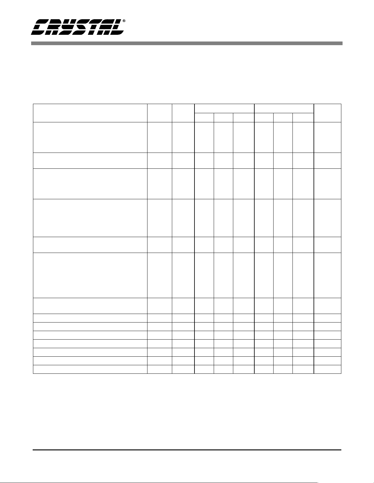
1. CHARACTERISTICS AND SPECIFICATIONS
AUDIO ANALOG CHARACTERISTICS (Standard test conditions unless otherwise noted:
T
Z
for ADC, 20- bit linear coding for DAC; Mixer registers set for unity gain.
= 25° C, AVdd = 5.0 V ±5%, DVdd = 3.3 V ±5%; 1 kHz Input Sine wave; Sample Frequency, Fs = 48 kHz;
ambient
=10 kΩ/680 pF load CDL = 18 pF load (Note 1); Measurement bandwidth is 20 Hz - 20 kHz, 18-bit linear coding
AL
CS4294-KQ CS4294-JQ
UnitMin Typ Max Min Typ Max
Parameter (Note 2) Symbol
Path
(Note 3)
Full Scale Analog Input Voltage
Line Inputs
Mic Inputs (20 dB=0)
Mic Inputs (20 dB=1)
A-D
A-D
A-D
0.91
0.91
0.091
1.00
1.00
0.10
-
0.91
-
0.91
-
0.091
1.00
1.00
0.10
-
V
V
V
RMS
RMS
RMS
-
-
Full Scale Output Voltage (Note 4)
Line and Alternate Line Outputs D-A 0.91 1.0 1.13 0.91 1.0 1.13 V
RMS
Frequency Response
Analog Ac = ± 0.5 dB
DAC Ac = ± 0.5 dB
ADC Ac = ± 0.5 dB
FR A-A
D-A
A-D
20
20
20
-
-
-
20,000
20,000
20,000
20
20
20
-
-
-
20,000
20,000
20,000
Hz
Hz
Hz
Dynamic Range
dB FS A
Stereo Analog inputs to LINE_OUT
Mono Analog inputs to LINE_OUT
DAC Dynamic Range
ADC Dynamic Range
DR A-A
A-A
D-A
A-D
90
85
85
85
95
90
90
90
90
-
-
-
-
85
87
85
-
-
-
-
-
dB FS A
dB FS A
dB FS A
DAC SNR (-20 dB FS input w/
CCIR-RMS filter on output) SNR D-A - 63 - - - - dB
Total Harmonic Distortion + Noise
(-3 dB FS input signal):
Line/Alternate Line Output
DAC
ADC (all inputs except phone/mic)
ADC (phone/mic)
THD+N A-A
D-A
A-D
A-D
-94
-
-86
-
-87
-
-87
-
-80
-80
-80
-74
-
-
-
-
dB FS A
-74
dB FS A
-74
dB FS A
-74
-
dB FS A
-74
Power Supply Rejection Ratio
(1 kHz, 0.5 V
w/ 5 V DC offset)(Note 5) 40 60 - - 40 - dB
RMS
Interchannel Isolation 70 87 - - 87 - dB
Spurious Tone (Note 5) - -100 - - -100 - dB FS
Input Impedance (Note 5) 10 - - 10 - - k
Ω
External Load Impedance 10 - - 10 - - kΩ
Output Impedance (Note 5) - 730 - - 730 - Ω
Input Capacitance (Note 5) - 5 - - 5 - pF
Vrefout 2.0 2.3 2.4 2.0 2.3 2.4 V
Notes: 1. Z
refers to the analog output pin loading and CDL refers to the digital output pin loading.
AL
2. Parameter definitions are given in the Paramete r and Term Defini tions section.
3. Path refers to the signal path used to generate this data. These paths are defined in the Parameter and
Term Definition section.
4. Typical measured with Z
=47kΩ/680 pF load.
AL
5. This specification is guaranteed by silicon characterization, it is not production tested.
DS326PP4 5
CS4294
ABSOLUTE MAXIMUM RATINGS (AVss1 = AVss2 = DVss1 = DVss2 = 0 V)
Parameter Min Typ Max Unit
Power Supplies +3.3 V Digital
+5 V Digital
Analog
Total Power Dissipation (Supplies, Inputs, Outputs) - - 750 mW
Input Current per Pin (Except Supply Pins) -10 - 10 mA
Output Current per Pin (Except Supply Pins) -15 - 15 mA
Analog Input voltage -0.3 - AVdd + 0.3 V
Digital Input voltage -0.3 - DVdd + 0.3 V
Ambient Temperature (Power Applied) -55 - 110 °C
Storage Temperature -65 - 150 °C
RECOMMENDED OPERATING CONDITIONS (AVss1 = AVss2 = DVss1 = DVss2 = 0 V)
Parameter Symbol Min Typ Max Unit
Power Supplies +3.3 V Digital
+5 V Digital
Analog
Operating Current +3.3 V Digital
+5 V Digital
Analog
Operating Ambient Temperature 0 - 70 °C
DVdd1, DVdd2
DVdd1, DVdd2
AVdd1, AVdd2
DVdd1, DVdd2
DVdd1, DVdd2
AVdd1, AVdd2
-0.3
-0.3
-0.3
3.135
4.75
4.75
-
-
-
3.3
5
5
40
40
75
6.0
6.0
6.0
3.465
5.25
5.25
97.5
52
52
V
V
V
V
V
V
mA
mA
mA
MIXER CHARACTERISTICS (for CS4294-KQ only)
Parameter Min Typ Max Unit
Mixer Gain Range Span Line In, Aux, CD, Mic1
Line Out, Alternate Line Out
Step Size All volume controls - 1.5 - dB
-
-
46.5
94.5
-
-
dB
dB
DIGITAL CHARACTERISTICS (AVss = DVss = 0 V)
Parameter Symbol Min Typ Max Unit
DVdd = 3.3V
Low level input voltage V
High level input voltage V
High level output voltage V
Low level output voltage V
Input Leakage Current (AC-link inputs) -10 - 10 µA
Output Leakage Current (Tri-stated AC-link outputs) -10 - 10 µA
Output buffer drive current BIT_CLK
SDATA_IN, EAPD
DVdd = 5.0 V
Low level input voltage V
High level input voltage V
High level output voltage V
Low level output voltage V
Input Leakage Current (AC-link inputs) -10 - 10 µA
Output Leakage Current (Tri-stated AC-link outputs) -10 - 10 µA
Output buffer drive current BIT_CLK
SDATA_IN, EAPD
oh
oh
il
ih
ol
il
ih
ol
2.15 V
3.0 3.25 V
0.03 .35 V
24
4
3.25 V
4.5 4.95 V
-0.03.35V
24
4
0.8 V
mA
mA
0.8 V
mA
mA
6 DS326PP4
CS4294
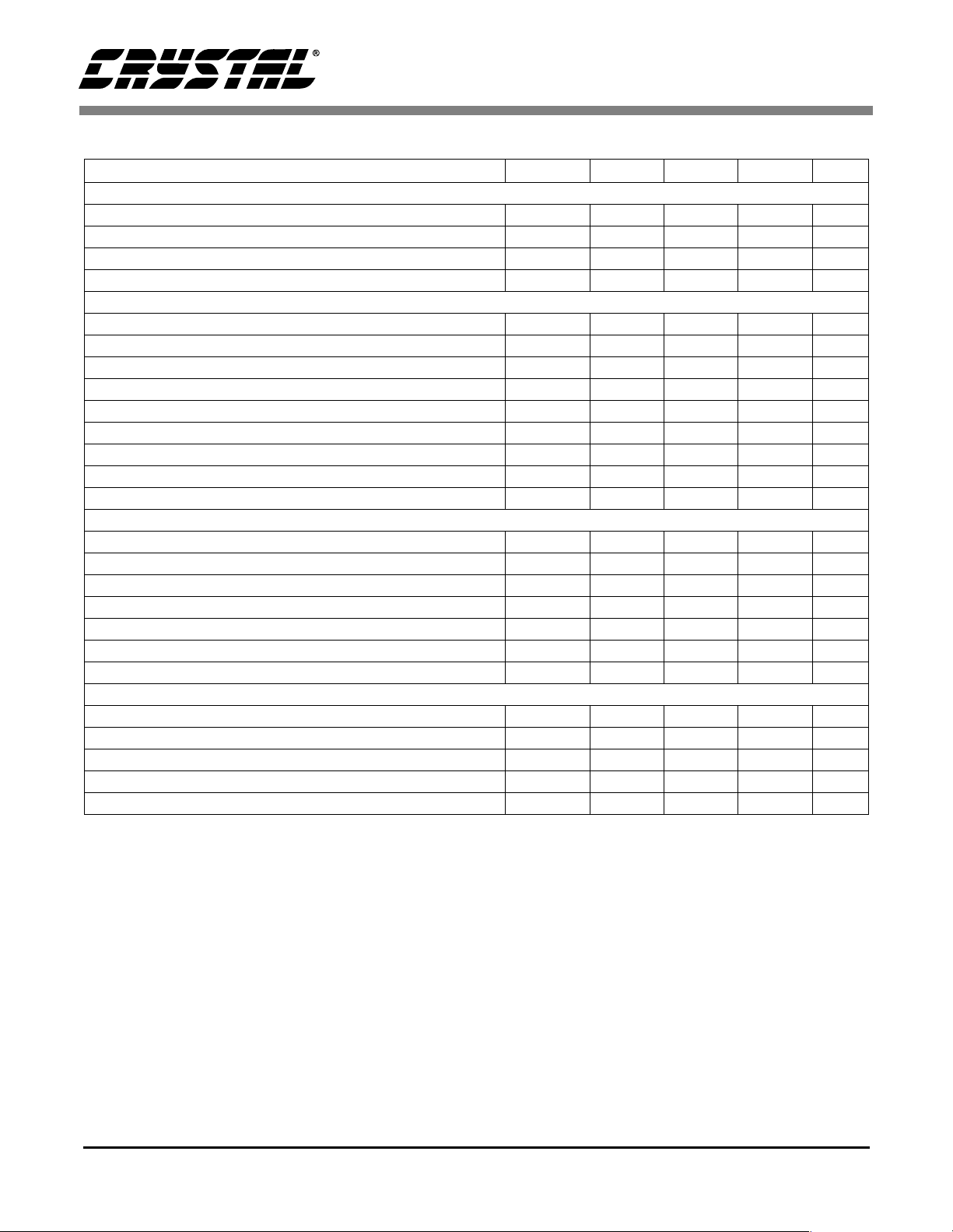
SERIAL PORT TIMING
Parameter Symbol Min Typ Max Unit
RESET# Timing
Vdd stable to RESET# inactive T
RESET# active low pulse width T
RESET# inactive to BIT_CLK star t-up delay T
1st SYNC active to CODEC READY set T
vdd2rst#
rst_low
rst2clk
sync2crd
Clocks
BIT_CLK frequency F
BIT_CLK period T
clk
clk_period
BIT_CLK output jitter (depends on XTAL_IN source) - - 750 ps
BIT_CLK high pulse width T
BIT_CLK low pulse width T
SYNC frequency F
SYNC period T
SYNC high pulse width T
SYNC low pulse width T
clk_high
clk_low
sync
sync_period
sync_high
sync_low
Data Setup and Hold
Output Propagation delay from rising edge of BIT_CLK T
Input setup time from falling edge of BIT_CLK T
Input hold time from falling edge of BIT_CLK T
Input Signal rise time T
Input Signal fall time T
Output Signal rise time (Note 5, 6) T
Output Signal fall time (Note 5, 6) T
co
isetup
ihold
irise
ifall
orise
ofall
Misc. Timing Parameters
End of Slot 2 to BIT_CLK, SDATA_IN low (PR4) T
SYNC pulse width (PR4) Warm Reset T
SYNC inactive (PR4) to BIT_CLK start-up delay T
Setup to trailing edge of RESET# (test mode) (Note 5) T
Rising edge of RESET# to Hi-Z delay (Note 5) T
s2_pdown
sync_pr4
sync2clk
setup2rst
off
Notes: 6. BIT_CLK measured with 47 Ω series termination and CL=50 pF.
5. ms
1.0 - - µs
25 120 - µs
- 62.4 - µs
- 12.288 - MHz
- 81.4 - ns
36 40.7 45 ns
36 40.7 45 ns
-48-kHz
- 20.8 - µs
-1.3-µs
- 19.5 - µs
- 6 12 ns
10 - - ns
0--ns
2-6ns
2-6ns
246ns
246ns
-.341.0µs
1.1 - - µs
162.8 350 - ns
15 - - ns
- - 25 ns
DS326PP4 7
BIT_CLK
RESET#
Vdd
T
rst_low
T
vdd2rst#
Figure 1. Power Up Timing
T
rst2clk
CS4294
BIT_CLK
SYNC
CODEC_READY
BIT_CLK
T
orise
SYNC
T
irise
T
sync2crd
Figure 2. Clocks
T
clk_highTclk_low
T
sync_high
T
T
clk_period
T
ifall
T
sync_low
ifall
T
sync_period
Figure 3. Codec Ready from Startup or F ault Conditi on
8 DS326PP4

BIT_CLK
BIT_CLK
SDATA_IN
SDATA_OUT,
SYNC
T
co
T
isetup
Figure 4. Data Setup and Hold
T
CS4294
ihold
SDATA_OUT
SDATA_IN
SYNC
Slot 1 Slot 2
Write to 0x20 Data PR4 Don’t Care
T
s2_pdown
T
Figure 5. PR4 Powerdown
RESET#
T
setup2rst
SDATA_OUT,
SYNC
T
off
sync_pr4
T
sync2clk
SDATA_IN,
BIT_CLK
Hi-Z
Figure 6. Test Mode
DS326PP4 9

CS4294
2. GENERAL DESCRIPTION
2.1 Overview
The CS4294 is a Mixed-Signal Audio Codec based
on the AC ‘97 1.0 Specification, and the AC ‘97
2.0 Extensions. It is designed to be paired with a
digital controller, typically located on the PCI bus.
The Controller is responsible for all communications between the CS4294 and the rest of the system. The CS4294 functions as an analog mixer, a
stereo audio ADC, a stereo audio DAC, and a control and digital stream interface to the Controller.
The CS4294 contains three distinct functional sections: Digital, Analog Audio, and Extended Analog
Audio.
The Digital section includes the AC-Link registers,
power management support, SYNC detection circuitry, and AC-Link serial port interface logic. The
Analog Audio section includes the analog input
multiplexer (mux), stereo input mixer, stereo output mixer, stereo ADCs, stereo DACs, and analog
volume controls. The Extended Audio section includes dual ADCs, dual DACs, GPIO control and
status, and power down and wake-up logic.
2.2 Modes of Operation
The CS4294 has two basic modes of operation.
Each mode allows varying functionality to meet a
wide variety of software and hardware configurations. On power up or system reset, the device reverts to the basic configuration Mode 0. The four
channel expansion and enhanced digital docking
are activate in Mode 1.
2.2.1 Mode 0
This is the default operating mode for the CS4294.
It supports the legacy AC ‘97 audio modes of operation including audio mixer, ADC’s, and DAC’s.
2.2.2 Mode 1
Mode 1 is the four channel expansion mode. The
second ADC/DAC pairs are utilized for enhanced
audio functionality. The second stereo DAC’s are
routed to the alternate line audio outputs providing
2 additional audio channels. The secondary ADC
inputs may be connected to the output of the analog
stereo input mixer for enhanced audio effect pr ocessing or enhanced digital docking in a note book
application.
3. DIGITAL SECTION
3.1 AC-Link
All communication with the Codec is established
with a 5-wire digital interface to the Controller chip
as shown in Figure 7. All clocking for the serial
communication is synchronous to the BIT_CLK
signal. BIT_CLK is generated by the primary Codec and is used to slave the Controller and any secondary Codecs, if applicable. An AC-link audio
frame is a sequence of 256 serial bits organized into
13 groups referred to as ‘slots’. One frame consists
of one 16-bit slot and twelve 20-bit slots. During
each audio frame, data is passed bi-directionally
between the Codec and the Controller. The input
frame is driven from the Codec on the SDATA_IN
line. The output frame is driven from the Controller
SDATA_OUT line. Both input and output frames
contain the same number of bits and are organized
with the same ‘slot’ configuration. The input and
output frame have differing functions for each slot.
The Controller synchronizes the beginning of a
frame with the SYNC signal. In Figure 9 the position of each bit location within the frame is noted.
The first bit position in a new serial data frame is F0
and the last bit position in the serial data frame is
F255. When SYNC goes active (high) and is sampled active by the CS4294 (on the falling edge of
BIT_CLK), both devices are synchronized to a new
serial data frame. The data on the SDATA_OUT
pin at this clock edge is the final bit of the previous
frame’s serial data. On the next rising edge of
BIT_CLK, the first bit of Slot 0 is driven by the
Controller on the SDATA_OUT pin. The CS4294
latches in this data, as the first bit of the frame, on
10 DS326PP4
CS4294
CODEC
SYNC
BIT_CLK
SDATA_OUT
SDATA_IN
RESET#
Digital AC’97
Controller
Figure 7. AC-link Connections
the next falling edge of the BIT_CLK clock signal.
The Controller is also responsible for issuing reset
via the RESET# signal. After being reset, the Codec is responsible for flagging the C ontroller that it
is ready for operation after synchronizing its internal functions. The AC-link signals may be referenced to either 5 Volts or 3.3 Volts. The CS4294
must use the same digital supply voltage as the
Controller chip.
3.2 Control registers
All read accesses to the Codec are generated by requesting a register address (index number) in slot 1
of a SDATA_OUT frame. The following
SDATA_IN frame will contain the register content
in its slot 2. The write operation is identical with the
index in slot 1 and the write data in slot 2. The
AC ‘97 Frame Definition section details the function of each input and output frame. Individual register descriptions are found in the Register
Interface section.
AC-97 Register Interface
The CS4294 implements the AC ’97 Registers in
accordance with the AC ’97 2.0 Specification. See
the Register Interface section for details on the
CS4294’s register set.
4. ANALOG SECTION
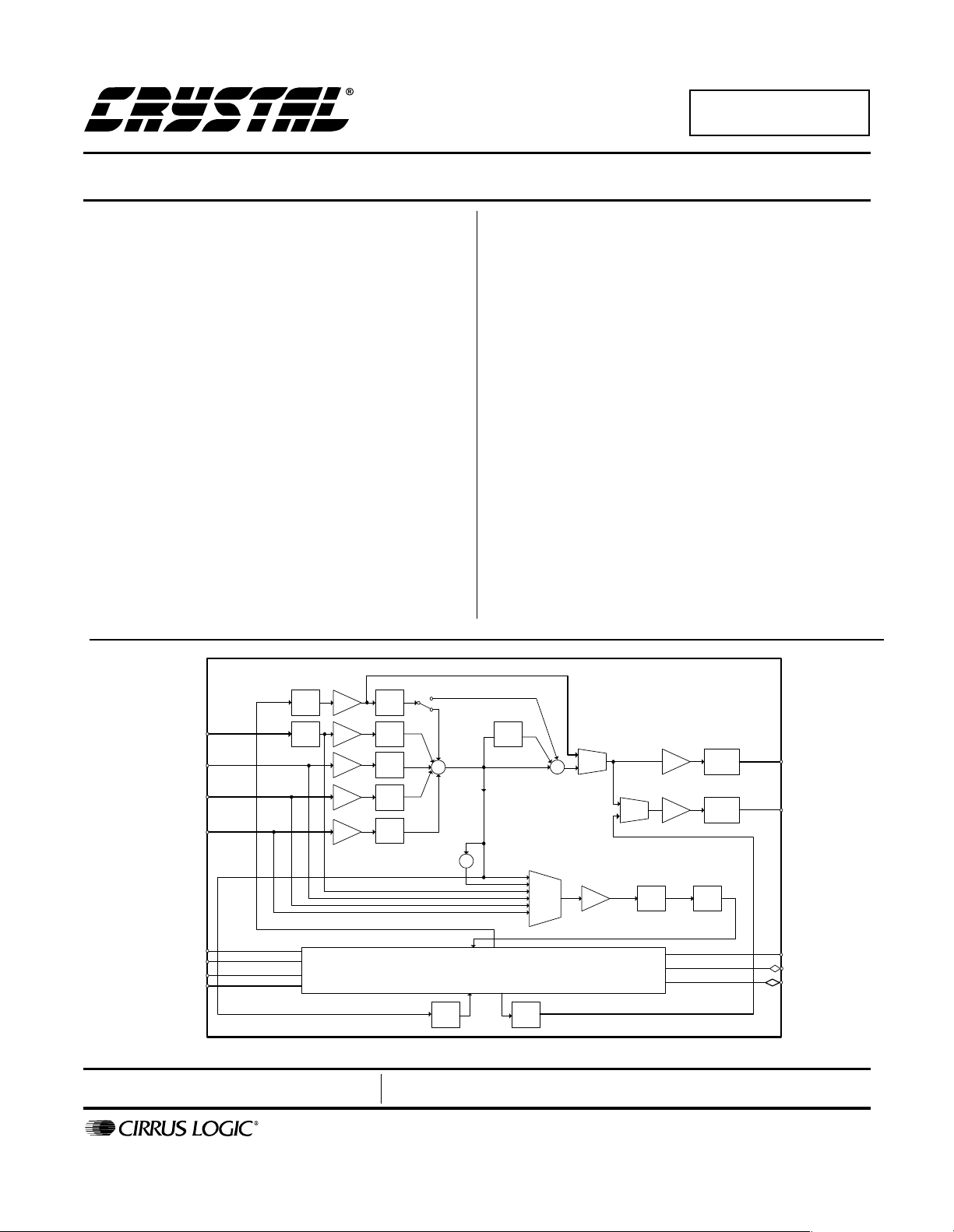
Please refer to Figure 8, Mixer diagram, for a highlevel graphical representation of the CS4294 analog mixer structure.
MIC1
LINE
CD
AUX
SDATA_OUT
RESET#
SYNC
Mode Control
CONVERTERS
PCM_OUT
2
/
2
/
2
/
3
/
2
/
MAIN D/A
DAC
+20dB
2
/
VOL MUTE
MUTE
VOL
MUTE
VOL
MUTE
VOL
MUTE
VOL
PCM OUT
PATH
STEREO
INPUT
MIXER
Σ
STEREO TO
MONO MIXER
AC-Link Interface
ADC DAC
3D
Σ
Figure 8. Mixer Diagram
STEREO
OUTPUT
ADC
INPUT
MUX
Σ
MIXER
MAIN ADC GA IN
VOL MUTE ADC
MASTER VOLUME
VOL
ALTERNATE VOLUME
VOL
2
/
6
/
OUTPUT
BUFFER
OUTPUT
BUFFER
2
/
2
/
LINE_OUT
ALT_LINE_OUT
SDATA_IN
BIT_CLK
GPIO
DS326PP4 11

CS4294
4.1 Audio Output Mixer
The stereo output mixer sums together the analog
outputs from the Input Mixer, stereo enhancement,
and the PCM DAC output. The stereo output mix is
sent to the LINE_OUT and ALT_LINE_OUT output pins of the CS4294. When the device is set to
Mode 1 or the EAM bit in AC Mode Control (Index
5Eh) is set, the secondary DAC outputs are routed
to ALT_LINE_OUT.
4.2 Audio Input Mux
The input multiplexer controls which analog input
is sent to the ADCs. The output of the input mux is
converted to stereo 18-bit digital PCM data and
sent to the Digital Controller chip in Slots 3 and 4
of the AC-Link SDATA_IN signal.
4.3 Audio Input Mixer
The input mixer is an analog mix of the analog input signals such as MIC, LINE_IN, etc., and the
PCM Audio DAC output. The output of the mixer
is routed to the ADC Input Mux, Audio Output
Mixer, and may be routed to the Extended Audio
ADC input.
4.4 Audio Volume Control
The volume control registers of the AC ’97 Register interface control analog input level to the input
mixer, the master volume level, and the alternate
volume level. All analog volume controls implement volume steps at nominally 1.5 dB per step.
The analog inputs allow a mixing range of +12 dB
of signal gain to -34.5 dB of signal attenuation. The
analog output volume controls allows from 0 dB to
-94.5 dB of attenuation.
5. AC ‘97
5.1 AC ‘97 Frame Definition
The AC Link is a bi-directional serial port with
thirteen time-division multiplexed slots in each direction. The first slot is 16 bits long and termed the
tag slot. Bits in the tag slot determine if the Codec
is ready and indicate which, if any, other slots contain valid data. Slots 1 through 11 are 20-bits long
and can contain audio data. Slot 12 contains data to
be written and read from GPIO. The serial data line
is defined from the Controller’s perspective, NOT
from the Audio Codec’s perspective.
5.2 AC-Link Serial Data Output Frame
In the serial data output frame, data is passed on the
SDATA_OUT pin TO the CS4294 FROM the
Controller. Figure 9 illustrates the serial port timing.
20.8 µS
(48 kHz)
F36 F57
F35
R/W 0 WD15
F36
00000
0
F56
LP19 LP18 RP19
F57
LC17 LC16 RC17RD15
F76
F97
X
F97
0
F255
X
F255
0
SYNC
BIT_CLK
Bit Frame Position:
SDATA_OUT
Bit Frame Position:
SDATA_IN
12.288 MHz
81.4 nS
F0 F1 F2 F16F15F14F13F12
F255
Valid
Frame
F0 F1 F2 F16F15F14F13F12 F35 F56 F76F255
Codec
Ready
Slot 1
Valid
Slot 1
Valid
X
0
Tag Phase Data Phase
Slot 2
Valid
Slot 2
Valid
00
Slot 0 Slot 1 Slot 2 Slot 3 Slot 4 Slots 5-12
SCRA1 SCRA0
Figure 9. AC-l ink Input and Output Framing
12 DS326PP4

CS4294
5.3 AC-Link Audio Output Frame
5.3.1 Serial Data Output Slot Tags (Slot 0)
Bit 1514131211109 8 76543210
Valid
Slot 1
Frame
Valid
Valid Frame
Slot [1:2] Valid
Slot [3:11] Valid
Slot 12 Valid
SCRA[1:0] Secondary Codec Register Access. Unlike the primary Codec, SCRA[1:0] indicate valid slot data when
Slot 2
Valid
Slot 3
Valid
Slot 4
Valid
Slot 5
Valid
Slot 6
Valid
Slot 7
Valid
Slot 8
Valid
Slot 9
Valid
Slot 10
Valid
Slot 11
Valid
Slot 12
Valid
SCRA1SCRA
0
Determines if any of the following slots contain either valid playback data for the Codec’s DACs, data
for read/write operation, or GPIO data. When set, at least one of the other AC-link slots contain valid
data. If this bit is clear, the remainder of the frame is ignored.
Indicates valid slot data when accessing the register set of the primary Codec (SCRA[1:0] = 00). For a
read operation, Slot 1 Valid is set when Register Address (Slot 1) contains valid data. For a write oper-
ation, Slot 1 Valid and Slot 2 Valid are set indicating Register Address ( Slo t 1) and Register Write Data
(Slot 2) contain valid data. The register address and write data must be valid within the same frame.
SCRA[1:0] must be cleared when accessing the primary Codec. The physical address of a Codec is
determined by the ID[1:0]# input pins which are reflected in the Extended Audio ID (Index 28h) register
and the Extended Codec ID (Index 3Ch) register.
If a Slot Valid bit is set, the named slot contains valid audio data. If the bit is clear, the slot will be ignored.
The definition of each slot is determined by the basic operating mode selected for the CS4294. For more
information, see the AC Mode Control (Index 5Eh) register.
If Slot 12 Valid is set, Slot 12 contains valid write data for the GPIO pins.
accessing the register set of a secondary Codec. The value set in SCRA[1:0] (01,10,11) determines
which of the three possible secondary Codecs is accessed. For a read operation, the SCRA[1:0] bits
are set when Register Address (Slot 1) contains valid data. For a write operation, SCRA[1:0] bits are
set when Register Address (Slot 1) and Register Write Data (Slot 2) contain valid data. The write operation requires the register address and the write data to be valid within the same frame. SCRA[1:0] must
be cleared wh en acce ssing t he prima ry Code c. They must al so be cl eared du ring the idle perio d where
no register read or write is pending. The physical address of a Codec is determined by the ID[1:0]# input
pins which are reflected in the Extended Audio ID (Index 28h) register and the Extended Codec ID (In-
dex 3Ch) register. The SCRA[1:0] bits are listed as the ID[1:0] bits in Slot 0 in the AC ‘97 specification.
5.3.2 Register Address (Slot 1)
Bit 191817161514131211109876543210
R/W# RI6 RI5 RI4 RI3 RI2 RI1 RI0
R/W # Read/Write#. Determines if a read (R/W# = 1) or write (R/W# = 0) operation is requested. For a read
operation, the following Input Frame will return the register index in the Read-Back Address Port (Slot
1) and the contents of the register in the Read-Back Data Port (Slot 2). A write operation does not return
any valid data in the following frame. If the R/W# bit = 0, data must be valid in both the Register Address
(Slot 1) and the Register Write Data (Slot 2)
RI[6:0] Register index/address. Registers can only be accessed on word boundaries; RI0 must be set to 0.
RI[6:0] must contain valid data during a frame when the Slot 1 Valid or SCRA[1:0] are set.
DS326PP4 13
during a frame when Slot [1:2] Valid or SCRA[1:0] are set.

CS4294
5.3.3 Register Write Data (Slot 2)
Bit 191817161514131211109876543210
WD15 WD14 WD13WD12 WD11WD10 WD9 WD8 WD7 WD6 WD5 WD4 WD3 WD2 WD1 WD0
WD[15:0] Codec register data for write operations. For read operations, this data is ignored. If R/W# = 0, data must
be valid in both the Register Address (Slot 1) and the Register Wr it e Dat a (Sl ot 2) during a frame when
the Slot [1:2] Valid = 11 or either SCRA[1:0] bit is set. Splitting the register address and the write data
across multiple frames is not permitted.
5.3.4 Playback Data (Slots 3-11)
Bit 191817161514131211109876543210
PD19 PD18 PD17 PD16 PD15 PD14 PD13 PD12 PD11 PD10 PD9 PD8 PD7 PD6 PD5 PD4 PD3 PD2 PD1 PD0
PD[19:0] 20-bit PCM playback (2’s complement) data for the left and right DACs. Any PCM data from the Con-
troller less than 20 bits should be left justified in the slot and zero-padded. Table 8 on page 28 lists the
definition of each respective slot. The mapping of a given slot is determined by the MD[1:0] bits found
in the AC Mode Control (Index 5Eh) register.
5.3.5 GPIO Data (Slot12)
Bit 191817161514131211109876543210
GP9 GP8 GP7 GP6 GP5 GP4 GP3 GP2 GP1 GP0
GP[9:0] GPIO Output Data. Output data is transferred to the GPIO pins every frame in Slot 12.
5.4 AC-Link Audio Input Frame
In the serial data input frame, data is passed on the SDATA_IN pin FROM the CS4294 to the AC ’97
Controller. The data format for the input frame is very similar to the output frame. Figure 9 illustrates
the serial port timing.
5.4.1 Serial Data Input Slot Tag Bits (Slot 0)
Bit 1514131211109 8 76543210
Codec
Ready
Codec Ready
Slot 1 Valid Tag
Slot 2 Valid Tag
Slot [3:11] Valid Tag
Slot 12 Valid Tag
Slot 1
Valid
Slot 2
Valid
Slot 3
Valid
Slot 4
Valid
Slot 5
Valid
Slot 6
Valid
Slot 7
Valid
Slot 8
Valid
Slot 9
Valid
Slot 10
Valid
Slot 11
Valid
Slot 12
Valid
Indicates the readiness of the CS4294’s AC-link and Control and Status registers. Immediately after a
Cold Reset this bit will be clear. Once the CS4294’s clocks and voltages are stable, this bit will be set.
Until the Codec Ready bit is set, no AC-link transactions should be attempted by the Controller. The
Codec Ready bit does not indicate readiness of the DACs, ADCs, Vref, or any other analog function.
Those must be checked in the Power Down Control/Status (Index 26h), Extended Audio Stat/Ctrl (Index
2Ah), and Extended Codec Stat/Ctrl (Index 3Eh) registers by the Controller before any access is made
to the mixer registers. Any accesses to the Codec while Codec Ready is clear is ignored.
Indicates Slot 1 contains a valid read back address.
Indicates Slot 2 contains valid register read data.
Indicates Slot [3:11] contains valid capture data from the Codec’s ADC.
Indicates Slot 12 contains valid read data of the GPIO Pin Status Register (Index 54h).
14 DS326PP4

CS4294
5.4.2 Read-Back Address Port (Slot 1)
Bit 191817161514131211109876 5 4 3210
RI6 RI5 RI4 RI3 RI2 RI1 RI0
RI[6:0] Register index. The Read-Back Address Port echoes the AC ’97 Register address when a register read
has been requested in the previous frame. The Codec will only echo the register index for a read access.
Write accesses will not return valid da ta in Slot 1.
5.4.3 Read-Back Data Port (Slot 2)
Bit 19 18 17 16 15 14 13 12 11 10 9 8 7 6 5 4 3 2 1 0
RD15 RD14 RD13 RD12 RD11 RD10 RD9 RD8 RD7 RD6 RD5 RD4 RD3 RD2 RD1 RD0
RD[15:0] 16-bit register value. The Read-Back Data Port contains the register data requested by the Controller
from the previous read request. All read requests will return the read address in the Read-Back Address
Port (Slot 1) and the register data in the Read-Back Data Port (Slot 2) on the following serial data frame.
5.4.4 PCM Capture Data (Slot 3-11)
Bit 191817161514131211109876543210
CD17 CD16CD15 CD14 CD13 CD12 CD11 CD10 CD9 CD8 CD7 CD6 CD5 CD4 CD3 CD2 CD1 CD0
CD[17:0] 18-bit PCM (2’s compliment) data. The mapping of a given slot to an ADC is determined by the state of
the MD[1:0] bits found in the AC Mode Control (Index 5Eh) register.
5.4.5 GPIO Pin Status (Slot 12)
Bit 191817161514131211109876543210
GI8 GI7 GI6 GI5 GI4 GI3 IRQ
GI[9:0] Status of the GPIO[8:3] pin.
IRQ Set when the GPIO generates a wake up or interrupt cycle. See GPIO Pin Wake Up Mask (Index 52h)
register.
The capture data in Slot [3:12] will only be valid when the respective slot valid bit is set in Slot 0.
5.5 AC ’97 Reset Modes
Three methods of resetting the CS4294, as defined
in the AC ’97 Specification, are supported: Cold
The timing of power-up/reset events is discussed in
detail in the Power Management section.
5.5.2 Warm AC ’97 Reset
AC ’97 Reset, Warm AC ’97 Reset, and AC ’97
Register Reset. A Cold AC ’97 Reset is required to
restart the AC-link when bit PR5 is set in the Power
Down Control/Status (Index 26h) register.
The CS4294 may also be reactivated when the AClink is powered down (refer to the PR4 bit description in the Power Management section) by a Warm
Reset. A Warm Reset allows the AC-link to be re-
5.5.1 Cold AC ‘97 Reset
A Cold Reset is performed by asserting RESET# in
accordance with the minimum timing specifications in the Serial Port Timing section. Once de-asserted, all of the Codec’s registers will be reset to
their default power-on states and the BIT_CLK
clock and SDATA_IN signals will be reactivated.
activated without losing information in the Codec’s
registers. Warm Reset is initiated when the SYNC
signal is driven high for at least 1 µs and then driven low in the absence of the BIT_CLK clock signal.
The BIT_CLK clock will not restart until at least 2
normal BIT_CLK clock periods (± 162.8 ns) after the SYNC signal is de-asserted.
DS326PP4 15

CS4294
5.5.3 AC ’97 Register Reset
The third reset mode provides a register reset to the
CS4294. This is available only when the CS4294’s
AC-link is active and the Codec Ready bit is set.
The audio and extended codec subsections may be
reset independently. Any write to Reset (Index 00h)
register will reset the audio subsection while any
write to Extended Codec Stat/Ctrl (Index 3Eh) register will reset the Extended Codec subsection. See
the respective register descriptions for additional
information.
5.6 AC-Link Protocol Violation - Loss of SYNC
The CS4294 is designed to handle SYNC protocol
violations. The following are situations where the
SYNC protocol has been violated:
• The SYNC signal is not sampled high for
exactly 16 BIT_CLK clock cycles at the
start of an audio frame.
• The SYNC signal is not sampled high on
the 256th BIT_CLK clock period after
the previous SYNC assertion.
• The SYNC signal goes active high before
the 256th BIT_CLK clock period after
the previous SYNC assertion.
Upon loss of synchronization with the Controller,
the Codec will mute all analog outputs and clear the
Codec Ready bit in the serial data input frame until
two valid frames are detected. Duri ng this detection
period, the Codec will ignore all register reads and
writes and will discontinue the transmission of
PCM capture data.
16 DS326PP4
CS4294
6. REGISTER INTERFACE
Certain register locations change definition based on the basic operating mode (Mode 0,1) selected by the
MD[1:0] bits found in the AC Mode Control (Index 5Eh) register. The reset default is Mode 0.
Reg
Num
00h Reset Mode 0
00h Reset Mode 1
02h Master Volume Mute ML5 ML4 ML3 ML2 ML1 ML0 MR5 MR4 MR3 MR2 MR1 MR0 8000h
04h Alternate Line Out V olu me Mute ML5 ML4 ML3 ML2 ML1 ML0 MR5 MR4 MR3 MR2 MR1 MR0 8000h
0Eh Mic Volume Mute 20dB GN4 GN3 GN2 GN1 GN0 8008h
10h Line In Volume Mute GL4 GL3 GL2 GL1 GL0 GR4 GR3 GR2 GR1 GR0 8808h
12h CD Volume Mute GL4 GL3 GL2 GL1 GL0 GR4 GR3 GR2 GR1 GR0 8808h
16h Aux Volume Mute GL4 GL3 GL2 GL1 GL0 GR4 GR3 GR2 GR1 GR0 8808h
18h PCM Out Vol Mute GL4 GL3 GL2 GL1 GL0 GR4 GR3 GR2 GR1 GR0 8808h
1Ah Record Select SL2 SL1 SL0 SR2 SR1 SR0 0000h
1Ch Record Gain Mute GL3 GL2 GL1 GL0 GR3 GR2 GR1 GR0 8000h
20h General Purpose POP SEE LPBK 0000h
22h Stereo Enhancement S3 S2 S1 S0 0000h
26h Powerdo wn Ct rl/ Stat PR6 PR5 PR4 PR3 PR2 PR1 PR0 REF ANL DAC ADC 000Fh
28h Ext’d Audio ID Mode 0 ID1 ID0 VRA x000h
28h Ext’d Audio ID Mode 1 ID1 ID0 LDAC SDAC CDAC VRA x1C0h
2Ah
2Ah
2Ch PCM Front DAC Rate SR15 SR14 SR13 SR12 SR11 SR10 SR9 SR8 SR7 SR6 SR5 SR4 SR3 SR2 SR1 SR0 BB80h
2Eh PCM Surround DAC Rate SR15 SR14 SR13 SR12 SR11 SR10 SR9 SR8 SR7 SR6 SR5 SR4 SR3 SR2 SR1 SR0 BB80h
30h PCM LFE DAC Rate SR15 SR14 SR13 SR12 SR11 SR10 SR9 SR8 SR7 SR6 SR5 SR4 SR3 SR2 SR1 SR0 BB80h
32h PCM Left/Right ADC Rate SR15 SR14 SR13 SR12 SR11 SR10 SR9 SR8 SR7 SR6 SR5 SR4 SR3 SR2 SR1 SR0 BB80h
36h Center LFE Volume Mute LFE5 LFE4 LFE3 LFE2 LFE1 LFE0 Mute CNT5 CNT4 CNT3 CNT2 CNT1 CNT0 8080h
38h LR Surround Volume Mute LSR5 LSR4 LSR3 LSR2 LSR1 LSR0 Mute RSR5 RSR4 RSR3 RSR2 RSR1 RSR0 8080h
3Ch Ext’d Codec ID ID1 ID0 x005h
3Eh
3Eh
40 Ext’d DAC1/ADC1 Rate SR15 SR14 SR13 SR12 SR11 SR10 SR9 SR8 SR7 SR6 SR5 SR4 SR3 SR2 SR1 SR0 BB80h
44 Ext’d DAC2/ADC2 Rate SR15 SR14 SR13 SR12 SR11 SR10 SR9 SR8 SR7 SR6 SR5 SR4 SR3 SR2 SR1 SR0 BB80h
46 Ext’d DAC1/ADC1 Level Mute DAC3 DAC2 DAC1 DAC0 Mute ADC3 ADC2 8080h
4A Ext’d DAC2/ADC2 Lev el Mute DAC3 DAC2 DAC1 DAC0 Mute ADC3 ADC2 8080h
4C GPIO Pin Configuration GC8 GC7 GC6 GC5 GC4 GC3 03FFh
4E GPIO Pin Polarity/Type GP8 GP7 GP6 GP5 GP4 GP3 FFFFh
50 GPIO Pin Sticky GS8 GS7 GS6 GS5 GS4 GS3 0000h
52 GPIO Pin Wakeup Mask GW8 GW7 GW6 GW5 GW4 GW3 0000h
54 GPIO Pin Status Gi8 GI7 GI6 GI5 GI4 GI3 xxxxh
Cirrus Defin ed Registers:
5A Crystal Revision / Fab 1 1 1 0 0302h
5E Slot Map Register E DM EAM DDM MD1 MD0 0000h
7Ch Vendor ID1 (CR) F7 F6 F5 F4 F3 F4 F1 F0 S7 S6 S5 S4 S3 S2 S1 S0 4352h
7Eh Vendor ID2(Y-) T7 T6 T5 T4 T3 T2 T1 T0 0 PID2 PID1 PID0 1 RID2 RID1 RID0 5 923h
Name D15 D14 D13 D12 D11 D10 D9 D8 D7 D6 D5 D4 D3 D2 D1 D0 Default
SE4 SE3 SE2 SE1 SE0 0 ID8 ID7 0 0 ID4 0 0 0 0
SE4 SE3 SE2 SE1 SE0 0 ID8 ID7 0 0 0 0 0 0 0
Ext’d Audio Stat/ Ctrl Mode
0
Ext’d Audio Stat/ Ctrl Mode
1
Ext’d Codec S tat/Ctrl
Mode 0
Ext’d Codec S tat/Ctrl
Mode 1
PRH PRG PRD PRC PRB PRA
PRK PRJ PRI LDAC SDAC CDAC 01C0h
PRG PRC PRB PRA
EDAC2EADC
2
EADC
2
EDAC1EAD
C1
EAD
C1
EREF GPIO 00CFh
EREF GPIO 0047h
1990h
1980h
0000h
Table 1. Mixer Registers
DS326PP4 17

CS4294
6.1 Register Descriptions
6.1.1 Reset (Index 00h)
Mode D15 D14 D13 D12 D11 D10 D9 D8 D7 D6 D5 D4 D3 D2 D1 D0
0 SE4SE3SE2SE1SE00ID8ID700ID40000
1 SE4SE3SE2SE1SE00ID8ID70000000
SE[4:0] Enhanced Stereo Technique.
00110 - Crystal 3D Stereo Enhancement.
ID8 set 18-bit ADC resolution.
ID7 set 20-bit DAC resolution.
ID4 set Headphone out support. (Alternate Line Output)
Read-onl y data
Mode 0 1990h
Mode 1 1980h
Any write to this register causes the audio control registers (Index 02h - 38h) and the Crystal specific
registers (Index 5Eh - 68h) to be reset forcing them to their default state. The mode control bits
MD[1:0] of the AC Mode Control (Index 5Eh) register are also cleared forcing the Codec to Mode 0
configuration. Reads return configuration information about the audio Codec
6.1.2 Master Volume (Index 02h)
D15 D14 D13 D12 D11 D10 D9 D8 D7 D6 D5 D4 D3 D2 D1 D0
Mute ML5 ML4 ML3 ML2 ML1 ML0 MR5 MR4 MR3 MR2 MR1 MR0
Mute Master mute for the LINE_OUT_L and the LINE_OUT_R output signals.
ML[5:0] Master Volume control for LINE_OUT_L pin. Least significant bit represents -1.5 dB with 00000 = 0 dB.
The total range is 0 dB to -94.5 dB.
MR[5:0] Master Volume control for LINE_OUT_R pin. Least significant bit represents -1.5 dB with 00000 = 0 dB.
The total range is 0 dB to -94.5 dB.
Default 8000h, corresponding to 0 dB attenuation and mute on.
In Mode 1 the LINE_OUT volume is controlled by the Left Right Surround (Index 38h) register in place
of Master Volume.
18 DS326PP4

CS4294
6.1.3 Alternate Volume (Index 04h)
D15 D14 D13 D12 D11 D10 D9 D8 D7 D6 D5 D4 D3 D2 D1 D0
Mute ML5 ML4 ML3 ML2 ML1 ML0 MR5 MR4 MR3 MR2 MR1 MR0
Mute Master mute for the ALT_LINE_OUT_L and the ALT_LINE_OUT_R output signals.
ML[5:0] Master Volume control for ALT_LINE_OUT_L pin. Least significant bit represents -1.5 dB with 00000 =
0 dB. The total range is 0 dB to -94.5 dB.
MR[5:0] Master Volume control for ALT_LINE_OUT_R pin. Least significant bit represents -1.5 dB with 00000 =
0 dB. The total range is 0 dB to -94.5 dB.
Default 8000h, corresponding to 0 dB attenuation and mute on.
In Mode 1 the ALT_LINE_OUT volume is controlled by the LFE/CNT Volume (Index 36h) register
in place of Alternate Volume.
ML[5:0]/MR[5:0]/MM[5:0]
Write
000000 000000 0 dB
000001 000001 -1.5 dB
…… ...
111111 111111 -94.5 dB
Table 2. Alternate Line-Out and Master Mono Attenuation
ML[5:0]/MR[5:0]/MM[5:0
Read Gain Level
6.1.4 Microphone Volume (Index 0Eh)
D15 D14 D13 D12 D11 D10 D9 D8 D7 D6 D5 D4 D3 D2 D1 D0
Mute 20dB GN4 GN3 GN2 GN1 GN0
Mute When set, mutes MIC signal.
GN[4:0] MIC Volume Control. Least significant bit represents 1.5 dB with 01000 = 0 dB. The total range is 12 dB
to -34.5 dB.
20dB Enables 20 dB microphone gain block.
Default 8008h, 0 dB attenuation and Mute set.
This register controls the gain level of the Microphone input source to the Input Mixer. It also controls the +20 dB gain block which connects to the input volume control and to the Input Record Mux.
The gain mapping for this register is shown in Table 3.
GN4 - GN0 Gain Level Mic Gain with 20dB = 1
00000 +12.0 dB +32.0 dB
00001 +10.5 dB 30.5 dB
…… ...
00111 +1.5 dB 21.5 dB
01000 0.0 dB 20.0 dB
01001 -1.5 dB 18.5 dB
…… ...
11111 -34.5 dB -14.5 dB
Table 3. Analog Mixer Input Gain Values
DS326PP4 19

CS4294
6.1.5 Stereo Analog Mixer Input Gain (Index’s 10h - 12h, 16h - 18h)
D15 D14 D13 D12 D11 D10 D9 D8 D7 D6 D5 D4 D3 D2 D1 D0
Mute GL4 GL3 GL2 GL1 GL0 GR4 GR3 GR2 GR1 GR0
Mute When set mutes the respective input. Setting this bit mutes both right and left inputs.
GL[4:0] Left Volume Control. Least significant bit represents 1.5 dB with 01000 = 0 dB. The total range is 12 dB
to -34.5dB. See Table 3.
GR[4:0] Right Volume Control. Least significant bit represents 1.5 dB with 01000 = 0 dB. The total range is 12
dB to -34.5 dB. See Table 3.
Default 8808h, 0 dB gain with Mute enabled.
These registers control the gain levels of the analog input sources to the Input Mixer. The analog inputs associated with registers 10h-18h are found in Table 4.
Register Index Function
10h Line IN Volume
12h CD Volume
16h Aux Volume
18h PCM Out Volume
Table 4. Stereo Volume Register Index
6.1.6 Input Mux Select (Index 1Ah)
D15 D14 D13 D12 D11 D10 D9 D8 D7 D6 D5 D4 D3 D2 D1 D0
SL2 SL1 SL0 SR2 SR1 SR0
SL[2:0] Left Channel ADC input source select.
SR[2:0] Right Channel ADC input source select.
Default 0000h, MIC inputs selected for both channels.
When capturing PCM data, this register controls the input MUX for the ADCs. Table 5 below lists
the possible values for each input.
Sx2 - Sx0 Record Source
0MIC
1 CD Input
2 Not Available
3 AUX Input
4 Line Input
5Stereo Mix
6 Mono Mix
7 Not Available
Table 5. Input Mux Selection
20 DS326PP4

CS4294
6.1.7 Record Gain (Index 1Ch)
D15 D14 D13 D12 D11 D10 D9 D8 D7 D6 D5 D4 D3 D2 D1 D0
Mute GL3 GL2 GL1 GL0 GR3 GR2 GR1 GR0
Mute When set, mutes the input to the ADCs.
GL[3:0] Left ADC gain. Least significant bit represents +1.5 dB with 0000 = 0 dB.
The total range is 0 dB to +22.5 dB.
GR[3:0] Right ADC gain. Least significant bit represents +1.5 dB with 0000 = 0 dB.
The total range is 0 dB to +22.5 dB.
Default 8000h, 0 dB gain with Mute on.
6.1.8 General Purpose (Index 20h)
D15 D14 D13 D12 D11 D10 D9 D8 D7 D6 D5 D4 D3 D2 D1 D0
POP SEE 0 LPBK
POP PCM Output Path. By default, the PCM output is mixed prior to the Stereo Enhancement. When set, the
PCM output is mixed after the Stereo Enhancement.
SEE Stereo Enhancement Enable. If set, enables the CrystalClear Stereo Enhancement.
LPBK Loopback. If set, enables Analog ADC/DAC Loopback Mode.
Default 0000h.
6.1.9 Stereo Enhancement Control (Index 22h)
D15 D14 D13 D12 D11 D10 D9 D8 D7 D6 D5 D4 D3 D2 D1 D0
S3 S2 S1 S0
S[3:0] Spacial Enhancement Depth. Spacial Enhancement is enabled by the Stereo Enhancement Enable bit
in the General Purpose (Index 20h) register.
0000 - No spacial enhancement.
1111 - Full spacial enhancement.
Default 0000h, no spacial enhancement added.
The Spacial Enhancements is not available on the ALT_LINE output when the codec is in Mode 1
or EAM is set. See the AC Mode Control (Index 5Eh) register for more detail.
DS326PP4 21

CS4294
6.1.10 Power Down Control/Status (Index 26h)
D15 D14 D13 D12 D11 D10 D9 D8 D7 D6 D5 D4 D3 D2 D1 D0
PR6 PR5 PR4 PR3 PR2 PR1 PR0 REF ANL DAC ADC
PR6 When set, the alternate line-out buffer is powered down.
PR5 When set, the internal master clock is disabled. The only way to recover from setting this bit is through
a cold AC ‘97 reset (driving the RESET# signal active).
PR4 When set, the AC link is powered down. The AC link can be restarted through a warm AC ‘97 reset using
the SYNC signal, or a cold AC ‘97 reset using the RESET# signal (the primary codec only).
PR3 When set, the analog mixer and voltage reference are powered down. When clearing this bit, the ANL,
ADC, and DAC bits should be checked before writing any mixer registers. Because the reference voltage is shared with the extended audio subsection, it will not power down unless the PRB bit is also set
in the Extended Codec Stat/Ctrl (Index 3Eh) register.
PR2 When set, the analog mixer is powered down (the voltage reference is still active). When clearing this
bit, the ANL bit should be checked before writing any mixer registers.
PR1 When set, the DACs are powered down. When clearing this bit, the DAC bit should be checked before
sending any data to the DACs.
PR0 When set, the ADCs and the ADC input muxes are powered down. When clearing this bit, no valid data
will be sent down the AC link until the ADC bit goes high.
REF Voltage Reference Ready Status. When set, indicates the voltage reference is at a nominal level.
ANL Analog Ready Status. When set, the analog output mixer, input multiplexer, and volume controls are
ready. When clear, no volume control registers should be written.
DAC DAC Ready Status. When set, the DACs are ready to receive data across the AC link. When clear, the
DACs will not accept any valid data.
ADC ADC Ready Status. When set, the ADCs are ready to send data across the AC link. When clear, no data
will be sent to the Controller.
Default 0000h, all blocks are powered on. The lower four bits will eventually change as the Codec finishes an
initialization and calibration sequence.
The PR[6:0] are power-down control for different sections of the Codec. The REF, ANL, DAC, and
ADC bits are status bits which, when set, indicate that a particular section of the Codec is ready. After
the Controller receives the Codec Ready bit in Slot 0, these status bits must be checked before writing
to any mixer registers.
22 DS326PP4

CS4294
6.1.11 Extended Audio ID (Index 28h)
Mode D15 D14 D13 D12 D11 D10 D9 D8 D7 D6 D5 D4 D3 D2 D1 D0
0ID1ID0 VRA
1 ID1 ID0 LDAC SDAC CDAC VRA
ID[1:0] Codec configuration ID. Primary is 00; Secondary is 01,10,or 11. This is a reflection of the ID[1:0]# con-
figuration pins. The state of the ID# pins are determined at power-up and are the inverse of the ID bits
in this register.
LDAC PCM LFE DAC. Indicates a LFE DAC is supported.
SDAC PCM Surround DAC. Indicates a Surround DAC is supported.
CDAC PCM Center DAC. Indicates a Center DAC is supported.
VRA Variable Rate Audio. This bit is clear indicating variable sample rates are not supported.
Read-onl y data
Mode 0 x000h. Where x is determined by the state of ID[1:0] input pins.
Mode 1 x1C0h.
6.1.12 Extended Audio Status/Control (Index 2Ah)
Mode D15 D14 D13 D12 D11 D10 D9 D8 D7 D6 D5 D4 D3 D2 D1 D0
0
1
000000000
0 PRK PRJ PRI 0 0 LDAC SDAC CDAC
CDAC PCM Center DAC Ready. When set, the Center DAC is ready.
LDAC PCM LFE DAC Ready. When set, the LFE DAC is ready.
SDAC PCM Surround DAC Ready. When set, the Surround DACs are ready.
PRI PCM Center DAC Disable. When set, the Center DAC is disabled.
PRJ PCM Surround DAC Disable. When set, the Surround DAC is disabled.
PRK PCM LFE DAC Disable. When set, the LFE DAC is disabled.
Default Mode 0 0000h
Mode 1 01C0h
CDAC, LDAC, and SDAC are read only bits.
6.1.13 PCM Front DAC Rate (Index 2Ch)
D15 D14 D13 D12 D11 D10 D9 D8 D7 D6 D5 D4 D3 D2 D1 D0
SR15 SR14 SR13 SR12 SR11 SR10 SR9 SR8 SR7 SR6 SR5 SR4 SR3 SR2 SR1 SR0
SR[15:0] Front DAC Sample Rate.
Default Read-only value BB80h, indicating 48 kHz sample rate.
6.1.14 PCM Surround DAC Rate (Index 2Eh)
D15 D14 D13 D12 D11 D10 D9 D8 D7 D6 D5 D4 D3 D2 D1 D0
SR15 SR14 SR13 SR12 SR11 SR10 SR9 SR8 SR7 SR6 SR5 SR4 SR3 SR2 SR1 SR0
SR[15:0] Surround DAC Sample Rate.
Default Read-only value BB80h, indicating 48 kHz sample rate.
DS326PP4 23

CS4294
6.1.15 PCM LFE DAC Rate (Index 30h)
D15 D14 D13 D12 D11 D10 D9 D8 D7 D6 D5 D4 D3 D2 D1 D0
SR15 SR14 SR13 SR12 SR11 SR10 SR9 SR8 SR7 SR6 SR5 SR4 SR3 SR2 SR1 SR0
SR[15:0] LFE DAC Sample Rate.
Default Read-only value BB80h, indicating 48 kHz sample rate.
6.1.16 PCM LR ADC Rate (Index 32h)
D15 D14 D13 D12 D11 D10 D9 D8 D7 D6 D5 D4 D3 D2 D1 D0
SR15 SR14 SR13 SR12 SR11 SR10 SR9 SR8 SR7 SR6 SR5 SR4 SR3 SR2 SR1 SR0
SR[15:0] LR ADC Sample Rate.
Default Read-only value BB80h, indicating 48 kHz sample rate.
6.1.17 Center LFE Volume (Index 36h)
D15 D14 D13 D12 D11 D10 D9 D8 D7 D6 D5 D4 D3 D2 D1 D0
Mute LFE5 LFE4 LFE3 LFE2 LFE1 LFE0 Mute CNT5 CNT4 CNT3 CNT2 CNT1 CNT0
LFE[5:0] LFE Volume. Least significant bit represents -1.5 dB with 00000 = 0 dB. The total range is 0 dB to -
94.5 dB.
CNT[5:0] Center Volume.Least significant bit represents -1.5 dB with 00000 = 0 dB. The total range is 0 dB to -
94.5 dB.
Default 8080h, indicating mute with 0 dB attenuation.
LFE[5:0]/LSR[5:0]
CNT[5:0]/RSR[5:0]
Write
000000 000000 0 dB
000001 000001 -1.5 dB
…… ...
111111 111111 -94.5 dB
Table 6. 6 Channel Volume Attenuation
LFE[5:0]/LSR[5:0]
CNT[5:0]/RSR[5:0]
Read
Gain Level
6.1.18 LR Surround Volume (Index 38h)
D15 D14 D13 D12 D11 D10 D9 D8 D7 D6 D5 D4 D3 D2 D1 D0
Mute LSR5 LSR4 LSR3 LSR2 LSR1 LSR0 Mute RSR5 RSR4 RSR3 RSR2 RSR1 RSR0
LSR[5:0] Left Surround Volume. Least significant bit represents -1.5 dB with 00000 = 0 dB. The total range is 0
dB to -94.5 dB.
RSR[5:0] Right Surround Volume. Least significant bit represents -1.5 dB with 00000 = 0 dB. The total range is 0
dB to -94.5 dB.
Default 8080h, indicating 0 dB attenuation.
24 DS326PP4

CS4294
6.1.19 Extended Codec ID (Index 3Ch)
Mode D15 D14 D13 D12 D11 D10 D9 D8 D7 D6 D5 D4 D3 D2 D1 D0
ID1 ID0
0
ID1 ID0
1
ID[1:0] Codec configuration ID. Primary is 00; Secondary is 01,10,or 11. This is a reflection of the configuration
pins. The state of the ID# pins are determined at power-up and are the inverse of the ID bits in this reg-
ister.
Default Mode 0 x005h
Mode 1 x000h Where x is determined by the state of ID[1:0] input pins.
The Extended Codec ID is a read/write register. Writing any value to this location issues a reset to
the Extended Codec registers (Index 3Ch-56h). The primary Audio registers are not reset by a write
to this location.
NOTE: All GPIO registers (Index 46h-54h) are reset by any write to this location.
6.1.20 Extended Codec Status/Control (Index 3Eh)
Mode D15 D14 D13 D12 D11 D10 D9 D8 D7 D6 D5 D4 D3 D2 D1 D0
PRH PRG PRD PRC PRB PRA EDAC2 EADC2 EDAC1 EADC1 EREF GPIO
0
1
PRH Extended DAC2. When set powers down the Extended DAC2.
PRG Extended ADC2. When set powers down the Extended ADC2.
PRD Extended DAC2. When set powers down the Extended DAC1.
PRC Extended ADC1. When set powers down the Extended ADC1.
PRB Extended ADC/DAC Reference. When set powers down the extended ADC/DAC reference. The ex-
PRA GPIO. When set the GPIO pins are tri-state and powered down. Slot 12 is marked invalid if the AC-link
EDAC2 Extended DAC2. When set indicates the Extended DAC2 is ready.
EADC2 Extended ADC2. When set indicates the Extended ADC2 is ready.
EDAC1 Extended DAC1. When set indicates the Extended DAC1 is ready.
EADC1 Extended ADC1. When set indicates the Extended ADC1 is ready.
EREF Extended ADC/DAC Reference. When set indicates the extended ADC/DAC reference is ready.
GPIO GPIO. When set the GPIO pins are ready. Slot 12 is marked valid.
Default Mode 0 x0CFh
PRG PRC PRB PRA EADC2 EADC1 EREF GPIO
tended ADC/DAC and audio share a common reference. The reference will not power down unless PR3
of the Power Down Ctrl/Stat (Index 26h) register is also set.
is active.
Mode 1 x047h Where x is determined by the state of ID[1:0] input pins.
PR[A:D,G:H] are read/write bits that provide power management of the extended codec subsection.
All remaining bits are read/only status indicating the subsystems are ready for operation. After reset
or issuing a change to the MD[1:0] of AC Mode (Index 5Eh) register, the respective status bits for
that mode will be clear until the subsystem becomes ready.
DS326PP4 25

CS4294
6.1.21 Extended Audio DAC1/ADC1 Rate (Index 40h)
D15 D14 D13 D12 D11 D10 D9 D8 D7 D6 D5 D4 D3 D2 D1 D0
SR15 SR14 SR13 SR12 SR11 SR10 SR9 SR8 SR7 SR6 SR5 SR4 SR3 SR2 SR1 SR0
SR[15:0] Extended Audio DAC1/ADC1 Sample Rate.
Default Read-only value BB80h, indicating 48 kHz sample rate.
6.1.22 Extended Audio DAC2/ADC2 (Index 44h)
D15 D14 D13 D12 D11 D10 D9 D8 D7 D6 D5 D4 D3 D2 D1 D0
SR15 SR14 SR13 SR12 SR11 SR10 SR9 SR8 SR7 SR6 SR5 SR4 SR3 SR2 SR1 SR0
SR[15:0] Extended Audio DAC2/ADC2 Sample Rate.
Default Read-only value BB80h, indicating 48 kHz sample rate.
6.1.23 Extended Audio DAC1/ADC1 Level (Index 46h)
D15 D14 D13 D12 D11 D10 D9 D8 D7 D6 D5 D4 D3 D2 D1 D0
Mute DAC3 DAC2 DAC1 DAC0 Mute ADC3 ADC2
Mute[D15] Mute. Mutes the input of Extended Audio DAC1.
Mute[D7] Mute. Mutes the output of Extended Audio ADC1.
DAC[3:0] Extended Audio DAC1 attenuation. Least significant bit represents 1.5 dB with 00000 = 0 dB. The total
range is 0 dB to -22.5 dB.
ADC[3:2] Extended Audio ADC1 gain. Least significant bit represents 6 dB with 00 = 0 dB. The total range is 0 dB
to +18 dB.
Default 8080h indicating mute with 0 dB attenuation or gain.
When EAM of the AC Mode Control (Index 5Eh) is set, the Extended Audio DAC1 attenuation is
controlled by ML[4:0] of the Alternate Volume (Index 04h) register.
6.1.24 Extended AudioDAC2/ADC2 Level (Index 4Ah)
D15 D14 D13 D12 D11 D10 D9 D8 D7 D6 D5 D4 D3 D2 D1 D0
Mute DAC3 DAC2 DAC1 DAC0 Mute ADC3 ADC2
Mute[D15] Mute. Mutes the input of Extended Audio DAC2.
Mute[D7] Mute. Mutes the output of Extended Audio ADC2.
DAC[3:0] Extended Audio DAC2 attenuation. Least significant bit represents 1.5 dB with 00000 = 0 dB. The total
range is 0 dB to -22 dB.
ADC[3:2] Extended Audio ADC2 gain. Least significant bit represents 6 dB with 00 = 0 dB. The total range is 0 dB
to +18 dB.
Default 8080h indicating mute with 0 dB attenuation or gain.
When EAM of the AC Mode Control (Index 5Eh) is set, the Extended Audio DAC2 attenuation is
controlled by MR[4:0] of the Alternate Volume (Index 04h) register.
26 DS326PP4

CS4294
6.1.25 GPIO Pin Configuration (Index 4Ch)
D15 D14 D13 D12 D11 D10 D9 D8 D7 D6 D5 D4 D3 D2 D1 D0
000000resGC8GC7GC6GC5GC4GC3resresres
GC[9:0] GPIO Pin Configuration. When set defines the corresponding GPIO pin as an input
Default 03FFh
After a cold reset, power up, or extended codec register reset (see Extended Codec ID (Index 3Ch))
all GPIO pins are configured as inputs.
6.1.26 GPIO Pin Polarity/Type Configuration (Index 4Eh)
D15 D14 D13 D12 D11 D10 D9 D8 D7 D6 D5 D4 D3 D2 D1 D0
111111resGP8GP7GP6GP5GP4GP3resresres
GP[9:0] GPIO Pin Configuration. The definition of GP[8:3] changes based on the pin defined as an input or an
output by GC[8:3] of GPIO Pin Configuration (Index 4Ch).
Default FFFFh
When the GPIO pin is defined as an input, its status is reported in the GPIO Pin Status (Index 54h)
register as well as Slot 12.
GCx GPx Function
0 0 Output CMOS drive
0 1 Output Open drain
1 0 Input Active Low
1 1 Input Active High (default)
Table 7. GPIO Input/Output Configuration
6.1.27 GPIO Pin Sticky (Index 50h)
D15 D14 D13 D12 D11 D10 D9 D8 D7 D6 D5 D4 D3 D2 D1 D0
GS8 GS7 GS6 GS5 GS4 GS3
GS[8:3] GPIO Pin Sticky. If set, the GPIO pin input is latched.
Default 0000h
If a GPIO is defined as “sticky” the input requires a transition of the GPIO input pin to set the corresponding bit in Slot 12 and the GPIO Pin Status (Index 54h) register. When “sticky” is set the corresponding bit in GPIO Pin Polarity/Type Configuration (Index 4Ah) register determines which edge
of the GPIO pin will set GI[x]. If GP[x] is set, a low to high transition sets the GI[x] bit. A high to
low transition sets GI[x] if GP[x] is clea r. Once set , writing a 0 to GI[x] will c lear the “sticky” input.
DS326PP4 27
CS4294
6.1.28 GPIO Pin Wakeup Mask (Index 4Ch)
D15 D14 D13 D12 D11 D10 D9 D8 D7 D6 D5 D4 D3 D2 D1 D0
GW8 GW7 GW6 GW5 GW4 GW3
GW[8:3] Wake up mask. If set, allow the GPIO input to generate AC-LINK wake up protocol.
Default 0000h
The CS4294 has the ability to generate a “wake up” cycle by a transition of a GPIO pin when the
AC-Link has been powered down. If a mask bit is set, a one being set in the corresponding GPIO Pin
Status (Index 54h) will initiate a wake up interrupt. Bit 0 of SDATA_IN Slot 12 will be set indicating
a GPIO interrupt. GPIO pins must be defined as “input”, “sticky”, and the mas k set t o allow a GPIO
interrupt. The GPIO interrupt is cleared by writing a 0 to the respective status bit in GPIO Pin Status
(Index 54h) register.
6.1.29 GPIO Pin Status (Index 54h)
D15 D14 D13 D12 D11 D10 D9 D8 D7 D6 D5 D4 D3 D2 D1 D0
GI8 GI7 GI6 GI5 GI4 GI3
GI[8:3] GPIO pin status. Reflects the state of all GPIO pins either input or output. If the GPIO pin is defined as
an output, the respective bit reflects the state of SDATA_OUT Slot 12. If the GPIO pin is defined as an
input, the register is reflected in SDATA_IN Slot 12. GPIO output pins cannot be accessed by Slot 1,2
register access, only by SDATA_OUT Slot 12.
6.1.30 AC Mode Control (Index 5Eh)
D15 D14 D13 D12 D11 D10 D9 D8 D7 D6 D5 D4 D3 D2 D1 D0
EDM EAM DDM MD1 MD0
DDM DAC Direct Mode. This bit controls the source to the line and alternate line output drivers. When set, the
Left and Right DAC directly drive the line and alternate line outputs by bypassing the audio mixer. When
clear, the audio mixer is the source for the line and alternate line outputs.
EAM Extended Audio Mode. When set the output of EDAC2 and EDAC1 are mapped to the ALT_LINE OUT-
PUT. The Extended Audio DAC volumes are set by the Alternate Line Volume (Index 04h) register when
in this mode.
EDM Extended Docking Mode. When set the output of the analog input mixer is routed to the EADC1 and
EADC2 inputs. This allows any analog input mix to be digitized and routed to a second AC ‘97 codec or
allows the host controller to add effects processing to analog sources.
MD[1:0] Mode. Sets basic operating mode for the codec. This effects the mapping of the ADCs and DACs to AC-
LINK Slot locations. See the Mode of Operation subsection for additional detail. Table 8 below details
the Slot mapping.
Default 0000h
Mode Type MD[1:0]
0 Basic
Extended 4
1
Channel
0,0 Left Right Left Right
1,1
Audio
DAC1
343451151112
Sur’nd
Left
78346 9 5 1112
Audio
DAC2
Sur’nd
Right
Audio
ADC1
Left Right Center LFE
Audio
ADC2
Ext’d
DAC1
Ext’d
Left
DAC2
Ext’d
Ext’d
Right
Ext’d
ADC1
Left
Mixer
Left
Mixer
Ext’d
ADC2
Right
Mixer
Right
Mixer
GPIO
Table 8. Slot Assignments
28 DS326PP4

CS4294
6.1.31 Vendor ID1 (Index 7Ch)
D15 D14 D13 D12 D11 D10 D9 D8 D7 D6 D5 D4 D3 D2 D1 D0
F7 F6 F5 F4 F3 F2 F1 F0 S7 S6 S5 S4 S3 S2 S1 S0
F[7:0] First Character of Vendor ID.
43h - ASCII ‘C’ character.
S[7:0] Second Character of Vendor ID.
52h - ASCII ‘R’ character.
Default Read-only data 4352h.
6.1.32 Vendor ID2 (Index 7Eh)
D15 D14 D13 D12 D11 D10 D9 D8 D7 D6 D5 D4 D3 D2 D1 D0
T7 T6 T5 T4 T3 T2 T1 T0 0 PID2 PID1 PID0 1 RID2 RID1 RID0
T[7:0] Third Character of Vendor ID.
59h - ASCII ‘Y’ character.
PID[3:0] Part ID.
See Table 9 below.
RID[2:0] Revision ID
Default Read-only data 592Bh.
The two Vendor ID registers provide a means to determine the manufacturer of the AC ’97 Codec.
The first three bytes of the ID registers contain the ASCII code for the first 3 letters of Crystal (CRY).
The final byte of the Vendor ID2 register is divided into a Part ID field and a Revision field. Table 9
lists the Part ID’s defined to date.
PID3-PID0 D3 Part Name
000 CS4297
001 CS4297A
010 0 CS4298
010 1 CS4294
011 CS4299
Table 9. Reg. 7Eh Defined Part ID’s
DS326PP4 29

CS4294
7. ANALOG HARDWARE DESCRIPTION
The analog hardware consist of three line-level stereo inputs, one mono microphone input, and dual,
independent stereo line outputs. This section describes the analog hardware needed to interface
with these pins.
7.1 Line-Level Inputs
The analog inputs consist of three stereo analog inputs and one mono input. As shown in Figure 8, the
input to the ADCs comes from the Input Mux
which selects one of the following: Mic1 (Mono),
CD, Aux, Line In, Stereo Input Mix, or the Mono
Input Mix (Mono). Unused analog inputs should be
connected together and then connected through a
capacitor to analog ground or tied to the Vrefout
line directly.
The analog input mixer is designed to accommodate four stereo inputs and one mono input. These
inputs are: a stereo line-level input (LINE), a mono
microphone input (MIC), a stereo CD-ROM input
(CD), a stereo auxiliary line-level input (AUX),
and the PCM output from the DACs (if the POP bit
is cleared). Each of the stereo inputs has separate
volume controls for each channel and one mute
control for each left/right pair. The mono microphone input has one mute and one volume control.
The inputs to the output mixer are: the input mixer
output, the stereo enhanced mix, and the DAC output (if the POP bit is set).
All analog inputs to the CS4294, including
CD_GND, should be capacitively coupled to the
input pins.
Since many analog levels can be as large as
2V
to attenuate the analog input by 6 dB (to 1 V
, the circuit shown in Figure 10 can be used
RMS
RMS)
which is the maximum voltage allowed for all the
stereo line-level inputs: LINE_IN and AUX_IN.
The CD line-level inputs have an extra pin,
CD_GND, which provides a pseudo-differential
input for both CD_L and CD_R. This pin takes the
common-mode noise out of the CD inputs when
connected to the ground coming from the CD analog source. Connecting the CD pins as shown in
Figure 11 provides extra attenuation of common
mode noise coming from the CDROM drive, thereby producing a higher quality signal. One percent
resistors are recommended since the better the resistors match, the better the common-mode attenuation of unwanted signals. If CD is not used, the
inputs should be connected through AC capacitors
to analog ground or connected to Vrefout.
7.2 Microphone Level Inputs
The microphone level inputs include a selectable -
34.5 dB to +12 dB gain stage for interfacing to an
external microphone. An additional 20 dB gain
block is also available. Figure 12 illustrates a single-ended microphone input buffer circuit that will
support lower gain mics. The circuit in Figure 12
supports dynamic mics and phantom-powered mics
that use the right channel (ring) of the jack for power.
CDROM IN
6.8 k
Ω
6.8 k
Ω
6.8 k
Ω
Figure 10. Line Inputs Figure 11. Differential CDROM In
30 DS326PP4
1.0 µF
1.0
6.8 k
R
µ
F
L
Ω
6.8 k
6.8 k
(Allresistors1%)
Ω
3.4 k
Ω
Ω
6.8 k
Ω
3.4 k
1.0µF
2.0µF
Ω
1.0
6.8 k
µ
F
Ω
CD_L
CD_GND
CD_R

CS4294
7.3 Line Level Outputs
The analog output section provides a stereo linelevel output and an alternate stereo line-level output. LINE_OUT_L, LINE_OUT_R,
ALT_LINE_OUT_L, and ALT_LINE_OUT_R
outputs should be capacitively coupled to external
circuitry.
Each of the 4 analog outputs, if used in the design,
require 680 pF or larger NPO diele ctric capacitors
between the corresponding pin and AGND. Each
analog output is DC biased up to the Vrefout voltage signal reference which is nominally 2.2 V. This
requires that the output either be AC coupled to external circuitry (AC load must be greater than 10
kΩ) or DC coupled to a buffer op-amp biased at the
Vrefout voltage (see Figure 13 for the recommended headphone op-amp circuit).
7.4 Miscellaneous Analog Signals
The AFILT1 and AFILT2 pins must have a
1000 pF NPO capacitor (must not be smaller than
390 pF) to analog ground. These capacitors, along
with an internal resistor, provide a single-pole lowpass filter at the inputs to the ADCs. By placing
these filters at the input to the ADCs, low-pass filters at each analog input pin are not necessary.
The REFFLT pin lowers the noise of the internal
voltage reference. A 1 µF (must not be greater than
1 µF) and 0.1 µF capacitor to analog ground should
be connected with a short, wide trace to this pin. No
other connection should be made, as any coupling
onto this pin will degrade the analog performance
of the Codec. Likewise, digital signals should be
kept away from REFFLT for similar reasons.
The Vrefout pin is typically 2.2 V and provides a
common mode signal for single-supply external
circuits. Vrefout only supports light DC loads and
should be buffered if AC loading is needed. For
typical use, a 0.1 µF in parallel with a 1 µF capacitor should be connected to Vrefout.
+5 VA
+5 VA
1
68 k
Ω
AGND
100 k
2.7 k
4
3
5
2
1
AGND
CGND
Ω
220 pF 220 pF
X7R
AGND
0.068 µF
1
+
2
AGND
10 µF
U1A
8
MC33078D
3
+
2
-
4
Ω
47 k
Ω
6.8 k
Ω
+
AGND
+5 VA
5
+
6
-
AGND
1
2
220 pF
10 µF
U1B
MC33078D
8
7
4
47 k
Ω
AGND
47 k
47 k
X7R
Ω
Ω
1 µF
MIC1
Figure 12. PC ‘99 Microphone Pre-amplifier
DS326PP4 31
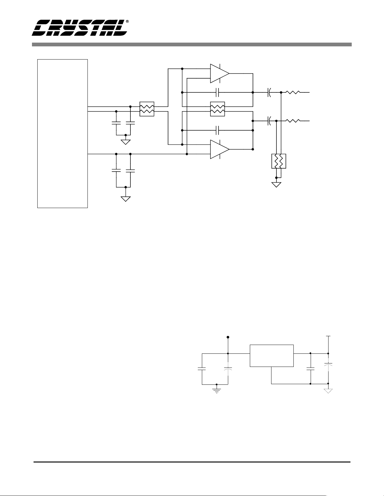
CS4294
ALT_LINE_OUT_R
ALT_LINE_OUT_L
Vrefout
0.1µF
Y5V
680pF
NPO
AGND
AGND
27k
41
Ω
2 3
680pF
NPO
1.0µF
Y5V
Figure 13. Headphones Driver
2
-
3
+
22pF
NPO
2 3
22pF
NPO
6
-
5
+
TDA1308
TDA1308
1
41
39k
Ω
7
220µF
ELEC
220µF
ELEC
10
Ω
+
+
4
3
1 2
AGND
1/4 WATT
10
1/4 WATT
47K
HP_OUT_R
Ω
HP_OUT_L
Ω
7.5 Power Supplies
The power supplies providing analog power should
be as clean as possible to minimize coupling into
the analog section which could degrade analog performance. The pins AVdd1 and AVdd2 supply
power to all the analog circuitry on the CS4294.
This 5 Volt analog supply should be generated
from a voltage regulator (7805 type) connected to a
+12 Volt supply. This helps isolate the analog circuitry from noise typically found on +5 V digital
supplies which power many digital circuits in a PC
environment. A typical voltage regulator circuit for
analog power using an MC78M05CDT is shown in
Figure 14.
The digital power pins DVdd1 and DVdd2 should
be connected to the same digital supply as the AC
’97 Controller’s AC-Link interface. Since the digital interface on the CS4294 may operate at either
3.3 V or 5 V, proper connection of these pins will
depend on the digital power supply of the AC ’97
Controller. connections (vias). The AC-Link digital interface connection traces should be routed
such that digital ground plane lies underneath these
signals (on the internal ground layer) from the AC
’97 Controller continuously to the CS4294.
Y5V
0.1µF
+12VD
MC78M05CDT
1
+
ELEC
10µF
IN
OUT
GND
2
Figure 14. Voltage Regulator
3
Y5V
0.1µF
+5VA
AGNDDGND
+
ELEC
10µF
32 DS326PP4

8. PIN DESCRIPTIONS
48 47 46 45 44 43 42 41 40 39 38 37
CS4294
AVs s4
AVs s5
FLT3D
FLTI
FLTO
GPIO8
GPIO7
GPIO6
GPIO5
GPIO4
AVdd4
AVs s 3
GPIO3
DVdd1
XTL_OUT
XTL_IN
SDATA_OUT
BIT_CLK
DVss2
SDATA_IN
DVdd2
SYNC
RESET#
1
2
3
4
5
6
7
8
9
10
11
CS4294-XQ
48-Pin TQFP
12
13 14 15 16 17 18 19 20 21 22 23 24
BCM#
AUX_L
CD_L
AUX_R
CD_GND
MIC1
CD_R
LINE_IN_L
LINE_IN_R
36
AVdd3
35
ID0#
34
ALT_LINE_OUT_R
33
ALT_LINE_OUT_L
32
AVss2DVss1
31
AVdd2
30
LINE_OUT_R
29
LINE_OUT_L
28
ID1#
27
AFLT2
26
AFLT1
25
Vrefout
AVss1
AVd d1
REFFLT
8.1 Digital I/O Pins RESET# - AC ’97 Chip Reset, Input
This active low signal is the asynchronous Cold Reset input to the CS4294. The CS4294 must
be reset before it can enter normal operating mode. When the PR4 bit of register 26h is set, the
RESET# rising edge will be used as an AC ‘97 2.1 Warm Reset only, preserving register
values.
SYNC - AC-link Serial Port Sync pulse, Input
This signal is the serial port timing signal for the AC-link of the CS4294. Its period is the
reciprocal of the sample rate of the CS4294, 48 kHz. This signal is generated by the AC ’97
Controller and is synchronous to BIT_CLK. SYNC is also an asynchronous input when the
CS4294 is in a PR4 powerdown state and is configured as a primary codec. A series
terminating resistor of 47 Ω should be connected on this signal close to the device driving the
signal.
DS326PP4 33

BIT_CLK - AC-link Serial Port Master Clock, Input/Outp ut
This input/output signal controls the master clock timing for the AC-link. In codec primary
mode, this signal is an output 12.288 MHz clock signal which is divided down by two from the
XTL_IN input clock pin. In codec secondary mode, this signal is an input which controls the
AC-link serial interface. In BIT_CLK mode, this signal generates all internal clocking
including the AC-link serial interface timing. A series terminating resistor of 47 Ω should be
connected on this signal close to the CS4294 in primary mode or close to the BIT_CLK source
if in secondary mode.
SDATA_OUT - AC-link Serial Data Input Stream to AC ‘97, Input
This input signal transmits the control information and digital audio output streams to be sent
to the DACs. The data is clocked into the CS4294 on the falling edge of BIT_CLK. A series
terminating resistor of 47 Ω should be connected on this signal close to the device driving the
input.
SDATA_IN - AC-link Serial Data Output Stream from AC ‘97, Output
This output signal transmits the status information and digital audio input streams from the
ADCs. The data is clocked out of the CS4294 on the rising edge of BIT_CLK. A series
terminating resistor of 47 Ω should be connected on this signal as close to the CS4294 as
possible.
CS4294
XTL_IN - Crystal Input
This pin accepts either a crystal, with the other pin attached to XTL_OUT, or an external
CMOS clock. XTL_IN must have a crystal or clock source attached for proper operation except
when operating in BIT_CLK mode. The crystal frequency must be 24.576 MHz and designed
for fundamental mode, parallel resonance operation.
XTL_OUT - Crystal Output
This pin is used for a crystal placed between this pin and XLT_IN. If an external clock is used
on XTL_IN or the codec is in BIT_CLK mode, this pin must be left floating with no traces or
components connected to it.
ID1#, ID0# - Codec ID, Inputs
These pins select the codec ID and mode of operation for the CS4294. They are sampled after
the rising edge of RESET# and not used after. These inputs have internal 100 kΩ pull-ups and
should be left floating for a logic 0 or tied to analog ground for a logic 1. The pins utilize
inverted logic, so the condition of both pins floating sets the codec to primary mode while any
other combination sets the codec to a secondary mode. In primary mode, the codec is always
clocked from an external crystal or an external oscillator connected to the XTL_IN and/or
XTL_OUT pins with BIT_CLK as an output. In secondary mode, the clocking mechanism is
determined by the state of the BCM# pin with BIT_CLK always being an input.
34 DS326PP4

BCM# - BIT_CLK Mode, Input
This pin selects the secondary mode clocking mechanism. BCM# is sampled after the rising
edge of RESET# and not used after. In codec secondary mode (ID1# and or ID0# grounded),
grounding this input will select BIT_CLK mode. In this mode, BIT_CLK is defined as an input
and all internal timing will be derived from the BIT_CLK signal and no connections should be
made to XTAL_IN and XTAL_OUT. When BCM# is floating, all timing will be derived from
the XTAL_IN pin. In this case, XTAL_IN must be synchronous to BIT_CLK. In primary mode,
BCM# must be left floating.
GPIO[8:3] - General Purpose Input/Output
These GPIO pins are used to control discrete digital functions. When a GPIO pin is configured
as an input, it behaves as a Schmitt trigger input with 350 mV of hysteresis at 5 V and 220 mV
of hysteresis at 3.3 V. When a GPIO pin in configured as an output, it may function as a
normal CMOS output (4 mA drive) or as an open drain output. GPIO pins power up in the high
impedance state (tri-state).
8.2 Analog I/O Pins MIC1 - Analog Mono Source, Input
CS4294
This analog input is a monophonic source to the analog output mixer. It is intended to be used
as a desktop microphone connection to the audio subsystem. The maximum allowable input is
1V
100 mV
(sinusoidal). If the 20 dB internal boost is enabled, the maximum allowable input is
RMS
(sinusoidal). This input is internally biased at the Vrefout voltage reference and
RMS
requires AC coupling to external circuitry. If this input is not used, it should be AC coupled to
analog ground.
LINE_IN_L and LINE_IN_R- Analog Line Source, Inputs
These inputs form a stereo input pair to the CS4294. The maximum allowable input is
1V
(sinusoidal). These inputs are internally biased at the Vrefout voltage reference. AC
RMS
coupling to external circuitry is required. If these inputs are not used, they should both be
connected to the Vrefout pin or both AC coupled, with separate AC coupling caps, to analog
ground.
CD_L and CD_R - Analog CD Source, Inputs
These inputs form a stereo input pair to the CS4294. It is intended to be used for the Red Book
CD audio connection to the audio subsystem. The maximum allowable input is 1 V
(sinusoidal). These inputs are internally biased at the Vrefout voltage reference. AC coupling to
external circuitry is required. If these inputs are not used, they should both be connected to the
Vrefout pin or both AC coupled, with separate AC coupling caps, to analog ground.
RMS
CD_GND - Analog CD Common Source, Input
This analog input is used to remove common mode noise from Red Book CD audio signals.
The impedance on the input signal path should be one half the impedance on the CD_L and
CD_R input paths. This pin requires AC coupling to external circuitry. If this input is not used,
it should be connected to the Vrefout pin or AC coupled to analog ground.
DS326PP4 35

AUX_L and AUX_R - Analog Auxiliary Source, Inputs
CS4294
These inputs form a stereo input pair to the CS4294. The maximum allowable input is 1 V
(sinusoidal). These inputs are internally biased at the Vrefout voltage reference. AC coupling to
external circuitry is required. If these inputs are not used, they should both be connected to the
Vrefout pin or both AC coupled, with separate AC coupling caps, to analog ground.
LINE_OUT_L and LINE_OUT_R - Analog Line Level Outputs
These signals are analog outputs from the stereo output mixer. The full scale output voltage for
output is nominally 1 V
and is internally biased at the Vrefout voltage reference. It is
RMS
required to either AC couple these pins to external circuitry or DC couple them to a buffer opamp biased at the Vrefout voltage. These pins need a 680 pF to 1000 pF NPO capacitor
attached to analog ground.
ALT_LINE_OUT_L and ALT_LINE_OUT_R - Analog Alternate Line Level Outputs
These signals are analog outputs from the stereo output mixer. The full scale output voltage for
each output is nominally 1 V
and is internally biased at the Vrefout voltage reference. It is
RMS
required to either AC couple these pins to external circuitry or DC couple them to a buffer opamp biased at the Vrefout voltage. These pins need a 680 pF to 1000 pF NPO capacitor
attached to analog ground.
8.3 Filter and Reference Pins REFFLT - Internal Reference Voltage, Input
RMS
This is the voltage reference used internal to the part. A 0.1 µF and a 1 µF (must not be larger
than 1 µF) capacitor with short, wide traces must be connected to this pin. No other
connections should be made to this pin.
Vrefout - Voltage Reference, Output
All analog inputs and outputs are centered around Vrefout which is nominally 2.2 Volts. This
pin may be used to level shift external circuitry, however any external loading should be
buffered.
AFLT1 - Left Channel Antialiasing Filter Input
This pin needs a 1000 pF NPO capacitor attached to analog ground.
AFLT2 - Right Channel Antialiasing Filter Input
This pin needs a 1000 pF NPO capacitor attached to analog ground.
FLTI - Enhanced Stereo Filter Input
A 1000 pF capacitor must be attached between this pin and FLTO if the Stereo Enhancement
function is used.
FLTO - Enhanced Stereo Filter Output
A 1000 pF capacitor must be attached between this pin and FLTI if the Stereo Enhancement
function is used.
36 DS326PP4

FLT3D - Enhanced Stereo Filter
A 0.01 µF capacitor must be attached from this pin to AGND if the Enhanced Stereo function
is used.
8.4 Power Supplies DVdd1, DVdd2 - Digital Supply Voltage
These pins provide the digital supply voltage for the AC-link section of the CS4294. These pins
may be tied to +5 V digital or to +3.3 V digital. The CS4294 and digital controller’s AC-link
should share a common digital supply.
DVss1, DVss2 - Digital Ground
These pins are the digital ground connection for the AC-link section of the CS4294. These pins
should be isolated from analog ground currents.
AVdd1, AVdd2, AVdd3, AVdd4 - Analog Supply Voltage
These pins provide the analog supply voltage for the analog and mixed signal sections of the
CS4294. These pins must be tied to +5 V analog supply. It is strongly recommended that +5 V
be generated from a voltage regulator to ensure proper supply currents and noise immunity
from the rest of the system.
CS4294
AVss1, AVss2, AVss3, AVss4, AVss5 - Analog Ground
These pins are the ground connection for the analog, mixed signal, and substrate sections of the
CS4294. These pins should be isolated from digital ground currents.
DS326PP4 37

9. PARAMETER AND TERM DEFINITIONS
AC ’97 Specification
Refers to the Audio Codec ‘97 Component Specification Ver 2.1 published by Intel
Corporation [].
AC ’97 Controller or Controller
Refers to the control chip which interfaces to the Codec’s AC-link. This has been also called
DC ’97 for Digital Controller ‘97 [].
AC ’97 Registers or Codec registers
Refers to the 64-field register map defined in the AC ’97 Specification.
ADC
Refers to a single Analog-to-Digital converter in the Codec. “ADCs” refers to the stereo pair of
Analog-to-Digital converters.
DAC
CS4294
®
A single Digital-to-Analog converter in the Codec “DACs” refers to the stereo pair of Digitalto-Analog converters.
SRC
Sample Rate converter. Converts data derived at one sample rate to a differing sample rate.
Codec
Refers to the chip containing the ADCs, DACs, and analog mixer. In this data sheet, the Codec
is the CS4297A9.
FFT
Fast Fourier Transform.
Resolution
The number of bits in the output words to the DACs, and in the input words to the ADCs.
Differential Nonlinearity
The worst case deviation from the ideal code width. Units in LSB.
dB FS A
dB FS is defined as dB relative to full-scale. The “A” indicates an A weighting filter was used.
38 DS326PP4

Frequency Response (FR)
FR is the deviation in signal level verses frequency. The 0 dB reference point is 1 kHz. The
amplitude corner, Ac, lists the maximum deviation in amplitude above and below the 1 kHz
reference point. The listed minimum and maximum frequencies are guaranteed to be within the
Ac from minimum frequency to maximum frequency inclusive.
Dynamic Range (DR)
DR is the ratio of the RMS full-scale signal level divided by the RMS sum of the noise floor,
in the presence of a signal, available at any instant in time (no change in gain settings between
measurements). Measured over a 20 Hz to 20 kHz bandwidth with units in dB FS A.
Total Harmonic Distortion plus Noise (THD+N)
THD+N is the ratio of the RMS sum of a ll non-fundamental frequency components, divided by
the RMS full-scale signal level. It is tested using a -3 dB FS input signal and is measured over
a 20 Hz to 20 kHz bandwidth with units in dB FS.
Signal to Noise Ratio (SNR)
SNR, similar to DR, is the ratio of an arbitrary sinusoidal input signal to the RMS sum of the
noise floor, in the presence of a signal. It is measured over a 20 Hz to 20 kHz bandwidth with
units in dB.
CS4294
Interchannel Isolation
The amount of 1 kHz signal present on the output of the grounded AC-coupled line input
channel with 1 kHz, 0 dB, signal present on the other line input channel. Units in dB.
Interchannel Gain Mismatch
For the ADCs, the difference in input voltage to get an equal code on both channels. For the
DACs, the difference in output voltages for each channel when both channels are fed the same
code. Units in dB.
PATHS
A-D: Analog in, through the ADC, onto the serial link.
D-A: Serial interface inputs through the DAC to the analog output.
A-A: Analog in to Analog out (analog mixer).
10.REFERENCES
Intel, Audio Codec ‘97 Component Specification, Revision 2.1, May 22,1998.
http://developer.intel.com/pc-supp
/platform/ac97/
DS326PP4 39

11.PACKAGE DIMENSIONS
48L LQFP PACKAGE DRAWING
D1
D
CS4294
E
E1
1
e
∝
B
A
A1
L
INCHES MILLIMETERS
DIM MIN NOM MAX MIN NOM MAX
A --- 0.055 0.063 --- 1.40 1.60
A1 0.002 0.004 0.006 0.05 0.10 0.15
B 0.007 0.002 0.011 0.17 0.20 0.27
D 0.343 0.354 0.366 8.70 9.0 BSC 9.30
D1 0.272 0.28 0.280 6.90 7.0 BSC 7.10
E 0.343 0.354 0.366 8.70 9.0 BSC 9.30
E1 0.272 0.28 0.280 6.90 7.0 BSC 7.10
e* 0.016 0.020 0.024 0.40 0.50 BSC 0.60
L 0.018 0.24 0.030 0.45 0.60 0.75
∝ 0.000° 4° 7.000° 0.00° 4° 7.00°
* Nominal pin pitch is 0.50 mm
Controlling dimension is mm.
JEDEC Designation: MS026
40 DS326PP4

• Notes •

 Loading...