

CS4270
24-Bit, 192 kHz Stereo Audio CODEC
D/A Features
High Performance
– 105 dB Dynamic Range
– -95 dB THD+N
Selectable Serial Audio Interface Formats
– Left-Justified up to 24-bit
– I²S up to 24-bit
– Right-Justified 16-, and 24-Bit
Control Output for External Muting
On-Chip Digital De-Emphasis
Popguard Technology
Multi-bit ∆Σ Conversion
Digital Volume Control
A/D Features
High Performance
– 105 dB Dynamic Range
– -95 dB THD+N
Multi-bit Delta Sigma Conversion
High-Pass Filter to remove DC Offsets
Selectable Serial Audio Interface Formats
– Left-Justified up to 24-bit
– I²S up to 24-bit
System Features
Direct Interface with Logic Levels 1.8 V to 5 V
Internal Digital Loopback
Stand-Alone or Control Port Functionality
Single-Ended Analog Architecture
Supports all Audio Sample Rates from 4 kHz to
216 kHz
Control Port Supply
1.8 V to 5 V
Hardware Mode or
2
I
C/SPI Software Mode
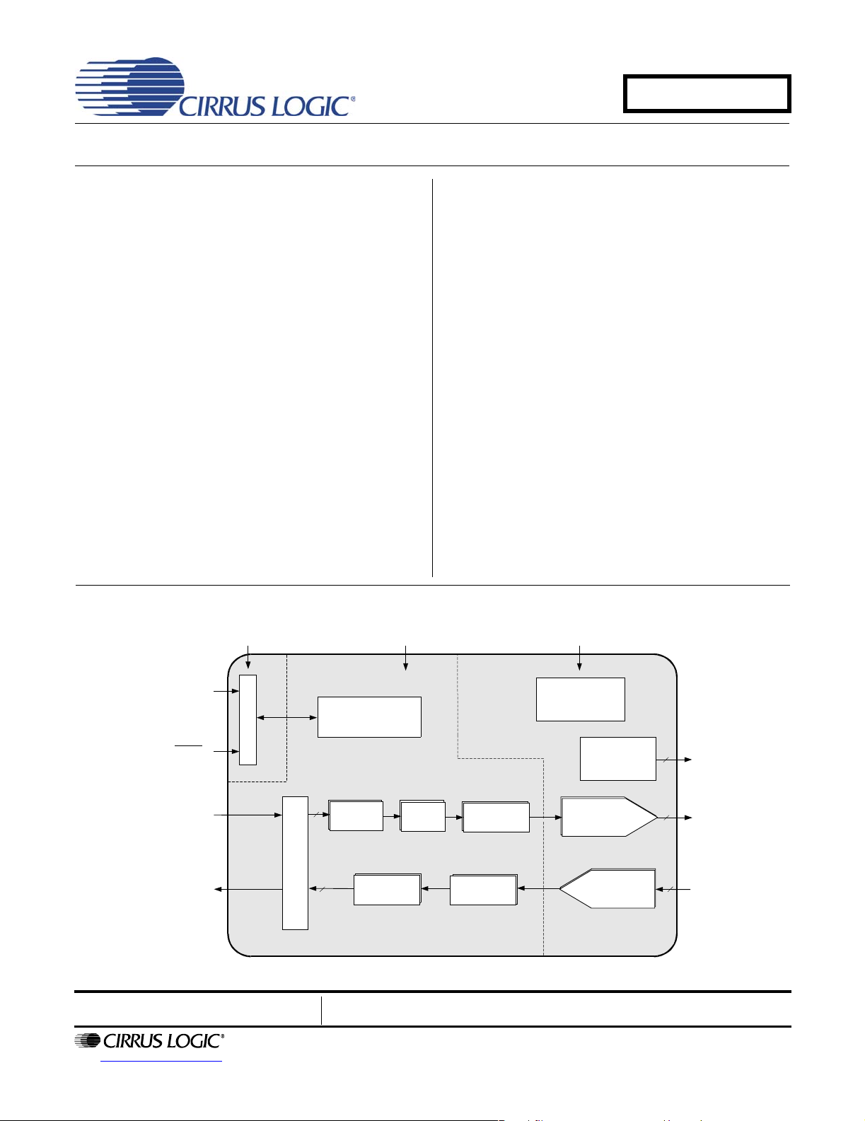
Control Data
Reset
PCM Serial
Audio Input
PCM Serial
Audio Output
Level Translator
Advance Product Information
http://www.cirrus.com
Register/Hardware
Configuration
Volume
2
Controls
Serial Interface
2
Digital Supply
3.3 V to 5 V
Digital
Filters
High-Pass
Filter
Multi-bit ∆Σ
Modulators
Digital
Filters
Analog Supply
3.3 V to 5 V
Internal Voltage
Reference
External Mute
Control
Switch-Cap
DAC and
Analog Filters
Switch-Cap
ADC
This document contains information for a new product.
Cirrus Logic reserves the right to modify this product without notice.
Copyright © Cirrus Logic, Inc. 2005
(All Rights Reserved)
2
2
2
Mute Signals
Single-Ended
Outputs
Single-Ended
Inputs
MAY '05
DS686A1
CS4270
Stand-Alone Mode Feature Set
System Features
– Serial Audio Port Master or Slave Operation
– Sing l e, Do ub le , or Quad -Speed Operation
D/A Features
– Auto-mute on Static Samples
– 44.1 kHz 50/15 µs De-emphasis Available
– Selectable Serial Audio Interface Formats
Left-Justified up to 24-bit
I²S up to 24-bit
A/D Features
– High-Pass Filter
– Selectable Serial Audio Interface Formats
Left-Justified up to 24-bit
I²S up to 24-bit
Software Mode Feature Set
System Features
– Serial Audio Port Master or Slave Operation
– Internal Digital Loopback Available
D/A Features
– Selectable Auto-mute
– 44.1-kHz De-emphasis Filters
– Configurable Muting Controls
– Volume Control
– Selectable Serial Audio Interface Formats
Left-Justified up to 24-bit
I²S up to 24-bit
Right Justified 16, and 24-bit
A/D Features
– Selectable High-Pass Filter or DC Offset
Calibration
– Selectable Serial Audio Interface Formats
Left-Justified up to 24-bit
I²S up to 24-bit
General Description
The CS4270 is a high-performance, integrated audio
CODEC. The CS4270 performs stereo analog-to-digital
(A/D) and digital-to-analog (D/A) conversion of up to
24-bit serial values at sample rates up to 216 kHz.
Standard 50/15 µs de-emphasis is available for sampling rates of 44.1 kHz for compatibility with digital audio
programs mastered using the 50/15 µs pre-emphasis
technique.
Integrated level translators allow easy interfacing between the CS4270 and other devices operating over a
wide range of logic levels.
Independently addressable high-pass filters are available for the right and left channel of the A/D. This allows
the A/D to be used in a wide variety of applications
where one audio channel and one DC measurement
channel is desired.
The CS4270’s wide dynamic range, negligible distortion, and low noise make it ideal for applications such as
DVD-recorders, digital televisions, set top boxes, effects processors, and automotive audio systems.
ORDERING INFORMATION
Product Description Package Pb-Free Grade Temp Range Cont ainer Order #
CS4270
CS4270
CDB4270 CS4270 Evaluation Board - - - - - CDB4270
2 DS686A1
24-Bit 192 kHz Stereo
Audio CODEC
24-Bit 192 kHz Stereo
Audio CODEC
24-TSSOP YES Commercial -10° to +85° C
24-TSSOP YES Commercial -40° to +85° C
Rail CS4270-CZZ
Tape & Reel CS4270-CZZR
Rail CS4270-DZZ
Tape & Reel CS4270-DZZR

TABLE OF CONTENTS
1. PIN DESCRIPTIONS - SOFTWARE MODE ............................................................................. 6
2. PIN DESCRIPTIONS - STAND-ALONE MODE ....................................................................... 7
3. CHARACTERISTICS AND SPECIFICATIONS ........................................................................ 8
SPECIFIED OPERATING CONDITIONS................................................................................. 8
ABSOLUTE MAXIMUM RATINGS........................................................................................... 8
THERMAL CHARACTERISTICS.............................................................................................. 8
DAC ANALOG CHARACTERISTICS (CS4270-CZZ)............................................................... 9
DAC ANALOG CHARACTERISTICS (CS4270-DZZ)............................................................... 9
DAC COMBINED INTERPOLATION & ON-CHIP ANALOG FILTER RESPONSE................ 11
ADC ANALOG CHARACTERISTICS (CS4270-CZZ)............................................................. 12
ADC ANALOG CHARACTERISTICS (CS4270-DZZ)............................................................. 13
ADC ANALOG CHARACTERISTICS - ALL MODES ............................................................. 14
ADC DIGITAL FILTER CHARACTERISTICS ........................................................................ 14
DC ELECTRICAL CHARACTERISTICS ....................................................... ... ... .... ... ... ... ... ... 15
DIGITAL CHARACTERISTICS............................................................................................... 16
SWITCHING CHARACTERISTICS - SERIAL AUDIO PORT................................................. 16
SWITCHING CHARACTERISTICS - I²C MODE CONTROL PORT....................................... 19
SWITCHING CHARACTERISTICS - SPI CONTROL PORT.................................................. 20
4. TYPICAL CONNECTION DIAGRAM ..................................................................................... 21
5. APPLICATIONS ..................................................................................................................... 22
5.1 Stand-Alone Mode ................. .... ... ... ... ... .... ... ... ... .............................................................22
5.1.1 Recommended Power-Up Sequence ................................................................. 22
5.1.2 Master/Slave Mode ............................................................................................. 22
5.1.3 System Clocking .............................. ... ... .......................................... .... ... ... ... ... ... 22
5.1.4 Clock Ratio Selection .......................................................................................... 23
5.1.5 Interpolation Filter .............................................................................................. 23
5.1.6 High-Pass Filter .. ... ... .... ... ... .......................................... ... ... .... ... ... ... .... ............... 23
5.1.7 Mode Selection & De-Emphasis ......................................................................... 24
5.1.8 Serial Audio Interface Format Selection ............................................................. 24
5.2 Control Port Mode .................................................. ... ... ... .......................................... ... . .. 24
5.2.1 Recommended Power-Up Sequence - Access to Control Port Mode ................ 24
5.2.2 Master / Slave Mode Selection ........................................................................... 24
5.2.3 System Clocking .............................. ... ... .......................................... .... ... ... ... ... ... 25
5.2.4 Clock Ratio Selection .......................................................................................... 25
5.2.5 Internal Digital Loopback .................................................................................... 26
5.2.6 Auto-Mute .... .......................................... .... ... ... ... .... ... ... ...................................... 26
5.2.7 High-Pass Filter and DC Offset Calibration ........................................................ 26
5.2.8 De-Emphasis ... ... ... ... .... ... ... .......................................... ... ... .... ... ... ... ................... 27
5.2.9 Oversampling Modes .... ... ... ... ... .... ... ... ... .... ... ............................................. ... ... ... 27
5.3 De-Emphasis Filter ................................................. ... ... ... ................................................ 27
5.4 Analog Connections ............................................... ... ... ... .... ... ... ... ... ................................ 28
5.4.1 Input Connections ............................................................................................... 28
5.4.2 Output Connections ...................................... ... ... .... ............................................ 29
5.5 Mute Control ....................................................... .... ... ... ... ................................................ 29
5.6 Synchronization of Multiple Devices ................................................................................ 30
5.7 Grounding and Power Supply Decoupling ....................................................................... 30
6. CONTROL PORT INTERFACE .............................................................................................. 31
6.1 SPI™ Mode ..................... ... ... .... ... ... ... ... .... .......................................... ... ... ... .... ... ... ......... 31
6.2 I²C Mode ................... .... ... ... ... .......................................... .... ... ... ... ... .... ... ......................... 32
7. REGISTER QUICK REFERENCE .......................................................................................... 33
8. REGISTER DESCRIPTION .................................................................................................... 34
8.1 Chip ID - Address 01h ..................................................................................................... 34
CS4270
DS686A1 3

CS4270
8.2 Power Control - Address 02h .......................................................................................... 34
8.2.1 Freeze (Bit 7) ...................................................................................................... 34
8.2.2 PDN_ADC (Bit 5) ................................................................................................ 34
8.2.3 PDN_DAC (Bit 1) ................................................................................................ 34
8.2.4 Power Down (Bit 0) ............................................................................................. 34
8.3 Mode Control - Address 03h ............................................................................................ 35
8.3.1 ADC Functional Mode & Master / Slave Mode (Bits 5:4) .................................... 35
8.3.2 Ratio Select (Bits 3:1) ......................................................................................... 35
8.3.3 PopGuard Disable (Bit 0) .................................................................................... 35
8.4 ADC and DAC Control - Address 04h ............................................................................. 35
8.4.1 ADC HPF Freeze A (Bit 7) .................................................................................. 35
8.4.2 ADC HPF Freeze B (Bit 6) .................................................................................. 36
8.4.3 Digital Loopback (Bit 5) ....................................................................................... 36
8.4.4 DAC Digital Interface Format (Bits 4:3) ............... ............. ............. ............. ......... 36
8.4.5 ADC Digital Interface Format (Bit 0) ................................................................... 36
8.5 Transition Control - Address 05h ..................................................................................... 37
8.5.1 DAC Single Volume (Bit 7) .................................................................................. 37
8.5.2 Soft Ramp or Zero Cross Enable (Bits 6:5) ........................................................ 37
8.5.3 Invert Signal Polarity (Bits 4:1) ............................................................................ 37
8.5.4 De-Emphasis Control (Bit 0) ............................................................................... 38
8.6 Mute Control - Address 06h ............................................................................................. 38
8.6.1 Auto-Mute (Bit 5) ................................................................................................. 38
8.6.2 ADC Channel A & B Mute (Bits 4:3) ................................................................... 38
8.6.3 Mute Polarity (Bit 2) ............................................................................................ 38
8.6.4 DAC Channel A & B Mute (Bits 1:0) ................................................................... 38
8.7 DAC Channel A Volume Control - Address 07h .............................................................. 39
8.8 DAC Channel B Volume Control - Address 08h .............................................................. 39
10. PACKAGE DIMENSIONS .................................................................................................... 41
11. APPENDIX ....................................................................................................................... 42
12. REVISION HISTORY ............................................................................................................ 48
LIST OF FIGURES
Figure 1. Output Test Load ....................................................................................................................... 10
Figure 2. Maximum Loading ...................................................................................................................... 10
Figure 3. Master Mode Serial Audio Port Timing ...................................................................................... 17
Figure 4. Slave Mode Serial Audio Port Timing ........................................................................................ 17
Figure 5. Format 0, Left Justified up to 24-Bit Data .................................................................................. 18
Figure 6. Format 1, I²S up to 24-Bit Data .................................................................................................. 18
Figure 7. Format 2, Right Justified 16-Bit Data. (Available in Control Port Mode only)
Format 3, Right Justified 24-Bit Data. (Available in Control Port Mode only ) ................ ................ ............ 18
Figure 8. I²C Mode Control Port Timing .................................................................................................... 19
Figure 9. SPI Control Port Timing .......................................... ... ... .... ... ... ... ... .... ......................................... 20
Figure 10. CS4270 Typical Connection Diagram ............................. ... ... ... ... .... ... ... ... .... ... ... ... ... .... ... ... ...... 21
Figure 11. De-Emphasis Curve ................................................................................................................. 27
Figure 12. CS4270 Recommended Analog Input Network .......................................................................28
Figure 13. CS5344 Example Analog Input Network .................................................................................. 29
Figure 14. CS4270 Recommended Analog Output Filter .......................................................................... 29
Figure 15. Suggested Active-Low Mute Circuit ......................................................................................... 30
Figure 16. Control Port Timing, SPI mode ............................................. ... ... .... ... ... ................................... 31
Figure 17. Control Port Timing, I²C Mode ................................................. ... .... ... ... ... .... ... ... ... ... .... ............ 32
Figure 18. De-Emphasis Curve ................................................................................................................. 38
Figure 19. DAC Single-Speed (fast) Stopband Rejection ................................... ... ... .... ... ... ... ... .... ... ... ... ... 42
Figure 20. DAC Single-Speed (fast) Transition Band ............................................................................... 42
4 DS686A1

CS4270
Figure 21. DAC Single-Speed (fast) Transition Band (detail) ................................................................... 42
Figure 22. DAC Single-Speed (fast) Passband Ripple .............................................................................42
Figure 23. DAC Single-Speed (slow) Stopband Rejection ........................................................................ 42
Figure 24. DAC Single-Speed (slow) Transition Band .............................................................................. 42
Figure 25. DAC Single-Speed (slow) Transition Band (detail) .................................................................. 43
Figure 26. DAC Single-Speed (slow) Passband Ripple ...................................................................... ... ... 43
Figure 27. DAC Double-Speed (fast) Stopband Rejection ........................................................................ 43
Figure 28. DAC Double-Speed (fast) Transition Band .............................................................................. 43
Figure 29. DAC Double-Speed (fast) Transition Band (detail) .................................................................. 43
Figure 30. DAC Double-Speed (fast) Passband Ripple ............................................................................ 43
Figure 31. DAC Double-Speed (slow) Stopband Rejection ...................................................................... 44
Figure 32. DAC Double-Speed (slow) Transition Band .............................................................................44
Figure 33. DAC Double-Speed (slow) Transition Band (detail) .............................. ................ ................ ... 44
Figure 34. DAC Double-Speed (slow) Passband Ripple ........................................................................... 44
Figure 35. DAC Quad-Speed (fast) Stopband Rejection .......................................................................... 44
Figure 36. DAC Quad-Speed (fast) Transition Band ................................................................................. 44
Figure 37. DAC Quad-Speed (fast) Transition Band (detail) .....................................................................45
Figure 38. DAC Quad-Speed (fast) Passband Ripple ...............................................................................45
Figure 39. DAC Quad-Speed (slow) Stopband Rejection ................................................................... ... ... 45
Figure 40. DAC Quad-Speed (slow) Transition Band ...............................................................................45
Figure 41. DAC Quad-Speed (slow) Transition Band (detail) ................................................................... 45
Figure 42. DAC Quad-Speed (slow) Passband Ripple ............................................................................. 45
Figure 43. ADC Single-Speed Mode Stopband Rejection ........................................................................ 46
Figure 44. ADC Single-Speed Mode Transition Band ...............................................................................46
Figure 45. ADC Single-Speed Mode Transition Band (Detail) .................................................................. 46
Figure 46. ADC Single-Speed Mode Passband Ripple ............................................................................. 46
Figure 47. ADC Double-Speed Mode Stopband Rejection ....................................................................... 46
Figure 48. ADC Double-Speed Mode Transition Band ............................................................................. 46
Figure 49. ADC Double-Speed Mode Transition Band (Detail) ................................................................. 47
Figure 50. ADC Double-Speed Mode Passband Ripple ........................................................................... 47
Figure 51. ADC Quad-Speed Mode Stopband Rejection ............................. .... ... ... ... .... ............................ 47
Figure 52. ADC Quad-Speed Mode Transition Band ................................... .... ... ... ... .... ... ... ... ... .... ... ... ...... 47
Figure 53. ADC Quad-Speed Mode Transition Band (Detail) ....................................... ... ... ... ... .... ... ... ... ... 47
Figure 54. ADC Quad-Speed Mode Passband Ripple .............................................................................. 47
LIST OF TABLES
Table 1. Speed Modes..... ... ... .... ... ... ... ...................................................................................................... 22
Table 2. Clock Ratios - Stand-Alone Mode............................................................................................... 23
Table 3. CS4270 Stand-Alone Mode Control............................................................................................ 24
Table 4. Speed Modes..... ... ... .... ... ... ... ...................................................................................................... 25
Table 5. Clock Ratios - Control Port Mode................................................................................................ 25
Table 6. Analog Input Design Parameters................................................................................................ 28
Table 7. Memory Address Pointer.................... ... .... ... ... ... .... ... ... ... .... ... ... ... ............................................. .. 32
Table 8. Functional Mode Selection................................. .... ... ... ... ............................................. .... ... ........ 35
Table 9. MCLK Divider Configuration........................................................................................................ 35
Table 10. DAC Digital Interface Formats ... ... ... ... .............................................. ... ... ... .... ... ... ... .................. 36
Table 11. ADC Digital Interface Formats ... ... ... ... .............................................. ... ... ... .... ... ... ... .................. 36
Table 12. Soft Cross or Zero Cross Mode Selection................................................................................. 37
Table 13. Digital Volume Control ........ .... ... ... .......................................................................................... .. 39
DS686A1 5
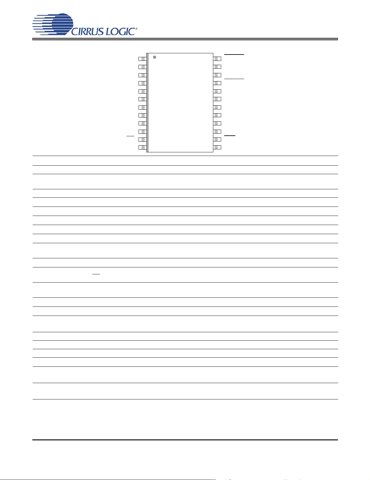
1. PIN DESCRIPTIONS - SOFTWARE MODE
CS4270
SDIN
LRCK
MCLK
SCLK
VD
DGND
SDOUT
VLC
SDA/CDOUT
SCL/CCLK
AD0/CS
AD1/CDIN
1
2
3
4
5
6
7
8
9
10
11
12
24
23
22
21
20
19
18
17
16
15
14
13
MUTEB
AOUTB
AOUTA
MUTEA
AGND
VA
FILT+
VQ
AINB
AINA
RST
AD2
Pin Name # Pin Description
SDIN 1 Serial Audio Data Input (Input) - Input for two’s complement serial audio data.
LRCK
MCLK 3 Master Clock (Input) - Clock source for the delta-sigma modulator and digital filters.
SCLK
VD
DGND
SDOUT
VLC
SDA/CDOUT
SCL/CCLK
AD0/CS
AD1/CDIN
AD2
RST
AINA
AINB
VQ 17 Quiescent Voltage (Output) - Filter connection for internal quiescent voltage.
FILT+ 18 Positive Voltage Reference (Output) - Positive reference voltage for the internal sampling circuits.
VA 19 Analog Power (Input) - Positive power for the analog sections.
AGND
MUTEA
MUTEB
AOUTA
AOUTB
Left Right Clock (Input/Output) - Determines which channel, Left or Right, is currently active on the
2
serial audio data line.
Serial Clock (Input/Output) - Serial clock for the serial audio interface.
4
Digital Power (Input) - Positive power supply for the digital section.
5
Digital Ground (Input) - Ground reference for the internal digital section.
6
Serial Audio Data Output (Output) - Output for two’s complement serial audio data.
7
Control Port Power (Input) - Determines the signal level for the control port.
8
Serial Control Data (Input/Output) - SDA is a data I/O in I²C mode. CDOUT is the output data line for
9
the control port interface in SPI mode.
Serial Control Port Clock (Input) - Serial clock for the serial control port.
10
Address Bit 0 (I²C) / Control Port Chip Select (SPI) (Input) - AD0 is a chip address pin in I²C mode.
11
CS is the chip select signal for SPI format.
Address Bit 1 (I²C) / Serial Control Data (Input) - AD1 is a chip address pin in I²C mode. CDIN is the
12
input data line for the control port i nt erf ace in SPI mode.
Address Bit 2 (I²C) (Input) - AD2 is a chip address pin in I²C mode.
13
Reset (Input) - The device enters a low power mode when low.
14
15
Analog Input (Input) - The full-scale analog input level is specified in the ADC Analog Characteristics
specification table.
16
Analog Ground (Input) - Ground reference. Must be connected to analog ground.
20
21
Mute Control (Output) - Each pin is active during power-up initialization, reset, muting, when master
clock to left/right clock frequency ratio is incorrect, or power-down.
24
22
Analog Audio Output (Output) - The full-scale output level is specified in the DAC Analog Character-
istics specification table.
23
6 DS686A1
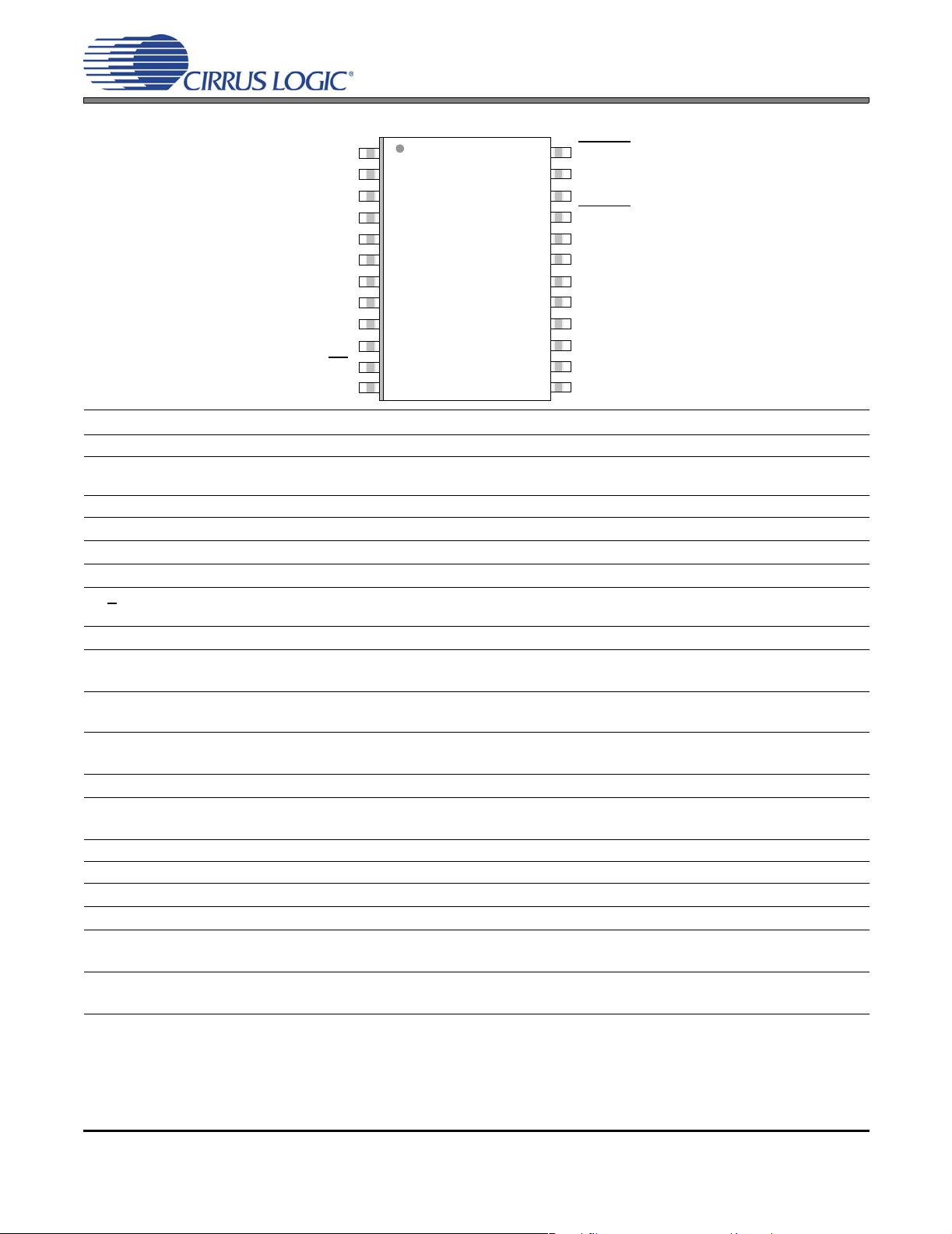
2. PIN DESCRIPTIONS - STAND-ALONE MODE
CS4270
SDIN
LRCK
MCLK
SCLK
VD
DGND
SDOUT
VLC
M1
M0
I²S/LJ
MDIV1
1
2
3
4
5
6
7
8
9
10
11
12
24
23
22
21
20
19
18
17
16
15
14
13
MUTEB
AOUTB
AOUTA
MUTEA
AGND
VA
FILT+
VQ
AINB
AINA
RST
MDIV2
Pin Name # Pin Description
SDIN 1 Serial Audio Data Input (Input) - Input for two’s complement serial audio data.
LRCK
MCLK 3 Master Clock (Input) - Clock source for the delta-sigma modulator and digital filters.
SCLK
VD
DGND
SDOUT
(M/S
)
VLC
M1
M0
I²S/LJ 11
MDIV1
MDIV2
RST
AINA
AINB
VQ 17 Quiescent Voltage (Output) - Filter connection for internal quiescent voltage.
FILT+ 18 Positive Voltage Reference (Output) - Positive reference voltage for the internal sampling circuits.
VA 19
AGND
MUTEA
MUTEB
AOUTA
AOUTB
Left Right Clock (Input/Output) - Determines which channel, Left or Right, is currently active on the
2
serial audio data line.
Serial Clock (Input/Output) - Serial clock for the serial audio interface.
4
Digital Power (Input) - Positive power supply for the digital section.
5
Digital Ground (Input) - Ground reference for the internal digital section.
6
Serial Audio Data Output (Output) - Output for two’s complement serial audio data. This pin must be
7
pulled-up or pulled-down to select Master or Slave Mode.
Control Port Power (Input) - Determines the signal level for the control port.
8
9
Mode Selection (Input) - Determines the operational mode of the device.
10
Serial Audio Interface Select (Input) - Selects either the left-justified orI²S format for the Serial Audio
Interface.
12
MCLK Divide (Input) - Configures MCLK divider to divide by 1, 1.5, 2, or 4.
13
Reset (Input) - The device enters a low power mode when low.
14
15
Analog Input (Input) - The full-scale analog input level is specified in the ADC Analog Characteristics
specification table.
16
Analog Power (Input) - Positive power for the analog sectio n s .
Analog Ground (Input) - Ground reference. Must be connected to analog ground.
20
21
Mute Control (Output) - Each pin is active during power-up initialization, reset, muting, when master
clock to left/right clock frequency ratio is incorrect, or power-down.
24
22
Analog Audio Output (Output) - The full-scale output level is specified in the DAC Analog Characteris-
tics specification table.
23
DS686A1 7
CS4270
3. CHARACTERISTICS AND SPECIFICATIONS
(All Min/Max characteristics and specificatio ns ar e gu a rant ee d over the Specified Operating Conditions. Typical
performance characteristics and spe cif icat ion s ar e de riv e d from measurements taken at nominal supply voltages
and T
= 25°C.)
A
SPECIFIED OPERATING CONDITIONS
(AGND = 0 V; all voltages with respect to ground.)
Parameters Symbol Min Nom Max Units
DC Power Supplies: Analog
Digital
Control Port Interface
Ambient Operating Temperature (Power Applied) (-CZZ)
(-DZZ)
VA
VD
VLC
T
A-CZZ
T
A-DZZ
3.1
3.1
1.7
-10
-40
5.0
3.3
3.3
-
-
5.25
5.25
5.25
+70
+85
V
V
V
°C
°C
ABSOLUTE MAXIMUM RATINGS
(AGND = DGND = 0 V, All voltages with respect to ground.) (Note 1)
Parameter Symbol Min Typ Max Units
DC Power Supplies: Analog
Digital
Control Port Interface
Input Current (Note 2)
Analog Input Voltage
Digital Input Voltage Control Port Interface
Digital Interface
Ambient Operating Temperature (Power Applied)
Storage Temperature
VLC
V
IND-C
V
IND-D
T
T
VA
VD
I
in
V
AC
stg
IN
-0.3
-0.3
-0.3
-
-
-
+6.0
+6.0
+6.0
-10 - +10 mA
AGND-0.7 - VA+0.7 V
-0.3
-0.3
-VLC+0.3
VD+0.3
-50 - +95 °C
-65 - +150 °C
V
V
V
V
V
Notes:
1. Operation beyond these limits may result in permanent damage to the device.
Normal operation is not guaranteed at these extremes.
2. Any pin except supplies. Transient currents of up to ±100 mA on the analog input pins will not cause SRC
latch-up.
THERMAL CHARACTERISTICS
Parameters Symbol Min Typ Max Units
Allowable Junction Temperature
Junction to Ambient Thermal Impedance (Note 3)
(Multi-layer PCB) TSSOP
(Multi-layer PCB) SOIC
(Single-layer PCB) TSSOP
(Single-layer PCB) SOIC
θ
JA-TM
θ
JA-SM
θ
JA-TS
θ
JA-SS
3. θJA is specified according to JEDEC specifications for multi-layer PCBs.
8 DS686A1
- - 135 °C
-
-
-
-
70
60
105
80
-
-
-
-
°C/W
°C/W
°C/W
°C/W

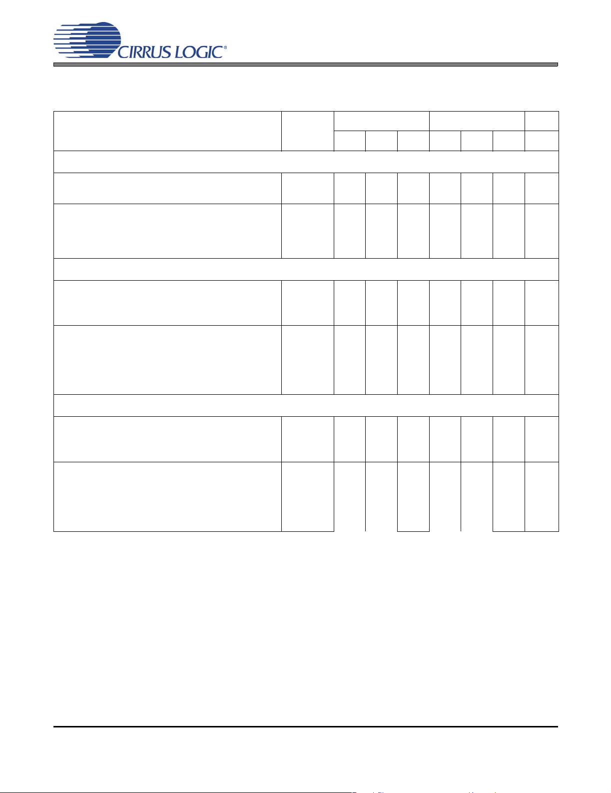
DAC ANALOG CHARACTERISTICS (CS4270-CZZ)
(Full-Scale Output Sine Wave, 997 Hz (Note 4), Fs = 48/96/192 kHz; Test load RL = 3 kΩ, CL = 10 pF
(see Figure 1). Measurement Bandwidth 10 Hz to 20 kHz, unless otherwise specified.)
VA = 5V VA = 3.3V
Parameter
Dynamic Range 18 to 24-Bit A-weighted
unweighted
16-Bit A-weighted
unweighted
Total Harmonic Distortion + Noise
18 to 24-Bit 0 dB
-20 dB
-60 dB
16-Bit 0 dB
-20 dB
-60 dB
Min Typ Max Min Typ Max Unit
99
96
90
87
105
102
96
93
-
-
-
-
-
-
-95
-82
-42
-93
-73
-33
-
-
-
-
-89
-76
-36
-87
-67
-27
97
94
90
87
-
-
-
-
-
-
103
100
96
93
-95
-80
-40
-93
-73
-33
DAC ANALOG CHARACTERISTICS (CS4270-DZZ)
(Full-Scale Output Sine Wave, 997 Hz (Note 4), Fs = 48/96/192 kHz; Test load RL = 3 kΩ, CL = 10 pF
(see Figure 1). Measurement Bandwidth 10 Hz to 20 kHz, unless otherwise specified.)
CS4270
-
-
-
-
-89
-74
-34
-87
-67
-27
dB
dB
dB
dB
dB
dB
dB
dB
dB
dB
Parameter
Dynamic Range 18 to 24-Bit A-weighted
unweighted
16-Bit A-weighted
unweighted
Total Harmonic Distortion + Noise
18 to 24-Bit 0 dB
-20 dB
-60 dB
16-Bit 0 dB
-20 dB
-60 dB
4. One-half LSB of triangular PDF dither added to data.
VA = 5V VA = 3.3V
Min Typ Max Min Typ Max Unit
95
92
86
83
105
102
96
93
-
-
-
-
-
-
-95
-82
-42
-93
-73
-33
-
-
-
-
-85
-72
-32
-83
-63
-23
93
90
86
83
-
-
-
-
-
-
103
100
96
93
-95
-80
-40
-93
-73
-33
-
-
-
-
-85
-70
-30
-83
-63
-23
dB
dB
dB
dB
dB
dB
dB
dB
dB
dB
DS686A1 9
DAC ANALOG CHARACTERISTICS - ALL MODES
Parameter Symbol Min Typ Max Unit
Interchannel Isolation (1 kHz)
DC Accuracy
Interchannel Gain Mismatch
Gain Drift
Analog Output
Full Scale Output Voltage
Max DC Current draw from AOUTA or AOUTB
Max AC-Load Resistance (see Figure 2) R
Max Load Capacitance (see Figure 2) C
Output Impedance of AOUTA and AOUTB
I
OUTmax
Z
L
L
OUT
-100 +100 ppm/°C
0.640•VA 0.688•VA 0.739•VA Vpp
CS4270
-100-dB
- 0.1 0.25 dB
-10-µA
-3-kΩ
-100-pF
-100-Ω
125
100
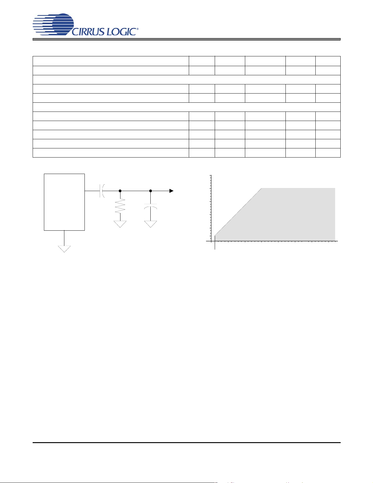
L
75
50
25
Ca p a c itive L o a d -- C (pF )
2.5
51015
3
Safe Operating
Resistive Load -- R (kΩ)
AGND
AOUTx
3.3 µF
V
out
R
L
C
L
Figure 1. Output Test Load Figure 2. Maximum Loading
Region
20
L
10 DS686A1
CS4270
DAC COMBINED INTERPOLATION & ON-CHIP ANALOG FILTER RESPONSE
(The filter characteristics have been normalized to the sample rate (Fs) and can be referenced to the desired sample rate by multiplying the given characteristic by Fs.) (See Note 5)
Parameter Symbol Min Typ Max Unit
Single-Speed Mode
Passband (
to -3 dB corner
Frequency Response 10 Hz to 20 kHz
StopBand
StopBand Attenuation (Note 7)
Group Delay
De-emphasis Error (Note 8) Fs = 32 kHz
Note 6) to -0.05 dB corner
Fs = 44.1 kHz
Fs = 48 kHz
Double-Speed Mode
Passband (Note 6) to -0.1 dB corner
to -3 dB corner
Frequency Response 10 Hz to 20 kHz
StopBand
StopBand Attenuation (Note 7)
Group Delay
Quad-Speed Mode
Passband (Note 6) to -0.1 dB corner
to -3 dB corner
Frequency Response 10 Hz to 20 kHz
StopBand
StopBand Attenuation (Note 7)
Group Delay
0
0
-.01 - +.08 dB
.5465 - - Fs
50 - - dB
tgd - 10/Fs - s
-
-
-
0
0
-.05 - +.2 dB
.5770 - - Fs
55 - - dB
tgd - 5/Fs - s
0
0
0 - +0.00004 dB
0.7 - - Fs
51 - - dB
tgd - 2.5/Fs - s
-
-
-
-
-
-
-
-
-
.4780
.4996
+1.5/+0
+.05/-.25
-.2/-.4
.4650
.4982
0.397
0.476
Fs
Fs
dB
dB
dB
Fs
Fs
Fs
Fs
5. Amplitude vs. Frequency plots of this data are available in Section 11. “Appendix” on page 42. See
Figures 19 through 42.
6. Response is clock dependent and will scale with Fs.
7. For Single-Speed Mode, the Measurement Bandwidth is 0.5465 Fs to 3 Fs.
For Double-Speed Mode, the Measurement Bandwidth is 0.577 Fs to 1.4 Fs.
For Quad-Speed Mode, the Measurement Bandwidth is 0.7 Fs to 1 Fs.
8. De-emphasis is available only in Single-Speed Mode.
DS686A1 11
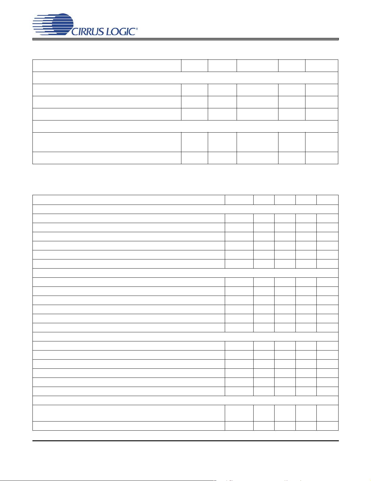
ADC ANALOG CHARACTERISTICS (CS4270-CZZ)
Measurement Bandwidth is 10 Hz to 20 kHz unless otherwise specified. Input is 1 kHz sine wave.
VA = 5V VA = 3.3V
CS4270
Parameter Symbol
Single-Speed Mode Fs = 48 kHz
Dynamic Range
unweighted
Total Harmonic Distortion + Noise
-1 dB
A-weighted
(Note 9)
-20 dB
-60 dB
Double-Speed Mode Fs = 96 kHz
Dynamic Range
unweighted
A-weighted
40 kHz bandwidth unweighted
Total Harmonic Distortion + Noise (Note 9)
-1 dB
-20 dB
-60 dB
40 kHz bandwidth -1 dB
Quad-Speed Mode Fs = 192 kHz
Dynamic Range
unweighted
A-weighted
40 kHz bandwidth unweighted
THD+N
THD+N
Min Typ Max Min Typ Max Unit
99
96
-
-
-
99
96
-
-
-
-
-
99
96
-
105
102
-98
-82
-42
105
102
99
-98
-82
-42
-95
105
102
99
-92
-92
-
-
-
-
-
-
-
-
-
-
-
-
-
9693102
99
-
-95
-
-79
-
-39
96
102
93
96
93
99
-
96
-
-95
-
-79
-
-39
-
-87
102
99
-
96
-89
-89
-
dB
-
dB
dB
-
dB
-
dB
-
dB
-
dB
-
dB
dB
-
dB
-
dB
-
dB
-
dB
-
dB
-
dB
Total Harmonic Distortion + Noise
40 kHz bandwidth -1 dB
(Note 9)
-1 dB
-20 dB
-60 dB
THD+N
-
-
-
-
-98
-82
-42
-95
-92
-
-95
-
-
-
-
-79
-
-39
-
-87
-89
dB
-
dB
-
dB
-
dB
9. Referred to the typical full-scale input voltage.
12 DS686A1
ADC ANALOG CHARACTERISTICS (CS4270-DZZ)
Measurement Bandwidth is 10 Hz to 20 kHz unless otherwise specified. Input is 1 kHz sine wave.
VA = 5V VA = 3.3V
CS4270
Parameter Symbol
Single-Speed Mode Fs = 48 kHz
Dynamic Range
unweighted
Total Harmonic Distortion + Noise
-1 dB
A-weighted
(Note 10)
-20 dB
-60 dB
Double-Speed Mode Fs = 96 kHz
Dynamic Range A-weighted
unweighted
40 kHz bandwidth unweighted
Total Harmonic Distortion + Noise
(Note 10)
-1 dB
-20 dB
-60 dB
40 kHz bandwidth -1 dB
Quad-Speed Mode Fs = 192 kHz
Dynamic Range
A-weighted
unweighted
40 kHz bandwidth unweighted
THD+N
THD+N
Min Typ Max Min Typ Max Unit
9794105
102
-
-98
-
-82
-
-42
97
105
94
102
-
99
-
-98
-
-82
-
-42
-
-95
97
105
94
102
-
99
-90
-90
-
-
-
-
-
-
-
-
-
-
-
-
-
9491102
99
-
-95
-
-79
-
-39
94
102
91
94
91
99
-
96
-
-95
-
-79
-
-39
-
-87
102
99
-
96
-87
-87
-
dB
-
dB
dB
-
dB
-
dB
-
dB
-
dB
-
dB
dB
-
dB
-
dB
-
dB
-
dB
-
dB
-
dB
Total Harmonic Distortion + Noise
40 kHz bandwidth -1 dB
(Note 10)
-1 dB
-20 dB
-60 dB
THD+N
-
-98
-
-82
-
-42
-
-95
-90
-
-95
-
-
-
-
-79
-
-39
-
-87
-87
dB
-
dB
-
dB
-
dB
10. Referred to the typical full-scale input voltage.
DS686A1 13
ADC ANALOG CHARACTERISTICS - ALL MODES
CS4270
Interchannel Isolation
-90-dB
DC Accuracy
Interchannel Gain Mismatch
Gain Error
Gain Drift
-0.1-dB
-3 - 3 %
-100 - +100 ppm/°C
Analog Input Characteristics
Full-scale Input Voltage
Input Impedance
ADC DIGITAL FILTER CHARACTERISTICS
0.54*V
A
-300-kΩ
(Note 11)
(Measurement Bandwidth is 10 Hz to 20 kHz unless otherwise specified)
Parameter Symbol Min Typ Max Unit
Single-Speed Mode
Passband (-0.1 dB) (Note 12)
Passband Ripple
Stopband (Note 12)
Stopband Attenuation
Group Delay
Interchannel Phase Deviation
Double-Speed Mode
Passband (-0.1 dB) (Note 12)
Passband Ripple
Stopband (Note 12)
Stopband Attenuation
Group Delay
Interchannel Phase Deviation
Quad-Speed Mode
Passband (-0.1 dB) (Note 12)
Passband Ripple
Stopband (Note 12)
Stopband Attenuation
Group Delay
Interchannel Phase Deviation
High-Pass Filter Characteristics
Frequency Response -3.0 dB
-0.13 dB (Note 13)
Phase Deviation @ 20 Hz (Note 13)
0.56*VA 0.58*V
0 - 0.47 Fs
-0.1 - 0.035 dB
0.58 - - Fs
-95 - - dB
t
gd
-12/Fs- s
- - 0.0001 deg
0 - 0.45 Fs
-0.1 - 0.035 dB
0.68 - - Fs
-92 - - dB
t
gd
-9/Fs- s
- - 0.0001 deg
0 - 0.24 Fs
-0.1 - 0.035 dB
0.78 - - Fs
-97 - - dB
t
gd
-5/Fs- s
- - 0.0001 deg
-120-
-10-deg
Vpp
A
Hz
-
Hz
14 DS686A1

Parameter Symbol Min Typ Max Unit
Passband Ripple
Filter Settling Time
--0dB
105/Fs s
11. Plots of this data are contained in Section 11. “Appendix” on page 42. See Figures 43 through 54.
12. The filter frequency response scales precisely with Fs.
13. Response shown is for Fs equal to 48 kHz. Filter characteristics scale with Fs.
DC ELECTRICAL CHARACTERISTICS
(TA = 25° C; AGND=DGND=0, all voltages with respect to ground; MLCK=12.288 MHz; Master Mode)
Parameter Symbol Min Typ Max Unit
Power Supply
Power Supply Current VA = 5 V
(Normal Operation) VA = 3.3 V
VD, VLC = 5 V
VD, VLC = 3.3 V
Power Supply Current VA = 5 V
(Power-Down Mode) (Note 14) VD, VLC = 5 V
Power Consumption
VA = 5 V, VD = VLC= 3.3 V Normal Operation
VA = 5 V, VD = VLC = 5 V Normal Operation
Power-Down Mode (Note 14)
Power Supply Rejection Ratio (1 kHz) (Note 15)
Common Mode Voltage
Nominal Common Mode Voltage
Maximum DC Current Source/Sink from VQ
VQ Output Impedance
Positive Voltage Reference
FILT+ Nominal Voltage
Maximum DC Current Source/Sink from FILT+
FILT+ Output Impedance
Mute Control
MUTEA, MUTEB Low-Level Output Voltage
MUTEA, MUTEB High-Level Output Voltage
Maximum MUTEA & MUTEB Drive Current
I
A
I
A
I
D
I
D
I
A
I
D
-
-
-
-
-
-
-
-
-
-
-
-
31
27
29
20
1.51
0.45
221
255
9.8
PSRR - 60 - dB
VQ - VA/2 - VDC
-1-µA
-25-kΩ
FILT + - VA - VDC
-10-µA
-18-kΩ
-0-V
-VA-V
-3-mA
40
35
38
29
-
-
296
-
323
CS4270
mA
mA
mA
mA
mA
mA
mW
mW
mW
14. Power Down Mode is defined as RST
= Low with all clocks and data lines held static.
15. Valid with the recommended capacitor values on FILT+ and VQ as shown in the Typical Connection Diagram.
DS686A1 15

DIGITAL CHARACTERISTICS
Parameter (Note 16) Symbol Min Typ Max Units
High-Level Input Voltage Serial Port
Control Port
Low-Level Input Voltage Serial Port
Control Port
High-Level Output Voltage at I
= 2 mA Serial Port
o
Control Port
MUTEA, MUTEB
Low-Level Output Voltage at Io = 2 mA
Input Leakage Current
V
IH
0.7xVD
0.7xVLC
V
IL
-
-
V
OH
VD - 1.0
VLC - 1.0
VA - 1.0
V
OL
I
in
--0.4V
-10 - 10 µA
16. Serial Port signals include: SCLK, LRCK, SDOUT, SDIN
Control Port signals include: SDA/CDOUT, SCL/CCLK, AD1/CDIN, AD0/CS
SWITCHING CHARACTERISTICS - SERIAL AUDIO PORT
(Logic "0" = AGND = 0 V; Logic "1" = VD, CL = 20 pF)
Parameter Symbol Min Typ Max Unit
Sample Rate Single-Speed Mode
Double-Speed Mode
Quad-Speed Mode
MCLK Specifications
MCLK Frequency Stand-Alone Mode
(Note 17) Control Port Mode
MCLK Duty Cycle
Master Mode
LRCK Duty Cycle
SCLK Period
SCLK Duty Cycle
SCLK falling to LRCK edge
SCLK falling to SDOUT valid
SDIN valid to SCLK rising setup time
SCLK rising to SDIN hold time
Slave Mode
LRCK Duty Cycle
SCLK Period
(
Note 17) Single-Speed Mode
Quad-Speed Mode
SCLK Duty Cycle
SCLK falling to LRCK edge
Double-Speed Mode
Fs
Fs
Fs
f
mclk
fmclk
t
slr
t
sdo
t
sdis
t
sdih
t
sclkw
t
sclkw
t
sclkw
t
slr
4
50
100
1.024
1.024
40 50 60 ns
-50-%
--s
-50-%
-10 - 10 ns
- - 32 ns
16 - - ns
20 - - ns
40 50 60 %
1
-------------------- -
128()Fs
1
-------------------- -
128()Fs
1
----------------- -
64()Fs
45 50 55 ns
-10 - 10 ns
, RST
-
-
-
-
-
1
----------------- -
64()Fs
-
-
-
-
-
-
-
-
-
-
-
-
0.2xVD
0.2xVLC
-
-
-
54
108
216
55.296
55.296
-
-
-
CS4270
V
V
V
V
V
V
V
kHz
kHz
kHz
MHz
MHz
s
s
s
16 DS686A1

CS4270
SCLK falling to SDOUT valid
SDIN valid to SCLK rising setup time
SCLK rising to SDIN hold time
t
sdo
t
sdis
t
sdih
- - 32 ns
16 - - ns
20 - - ns
17. In Control Port Mode, MCLK Frequency and Functional Mode Select bits must be configured according to
Table 5, Table 9, and Table 8
LRCK
Output
t
slr
SCLK
Output
t
sdo
SDOUT
t
sdis
t
sdih
SDIN
LRCK
Input
SCLK
Input
SDOUT
SDIN
Figure 3. Master Mode Serial Audio Port Timing
t
slr
t
t
sdis
sclkw
t
sdo
t
sdih
Figure 4. Slave Mode Serial Audio Port Timing
DS686A1 17

CS4270
LRCK
Left Channel
SCLK
SDATA +3 +2 +1
MSB
-1 -2 -3 -4 -5
+5 +4
Figure 5. Format 0, Left Justified up to 24-Bit Data
LRCK
SCLK
SDATA +3 +2 +1
MSB
-1 -2 -3 -4 -5
Left Channel
+5 +4
LSB
LSB
MSB
-1 -2 -3 -4
MSB
-1 -2 -3 -4
Right Channel
+3 +2 +1
+5 +4
Right Channel
+3 +2 +1
+5 +4
LSB
LSB
LRCK
SCLK
SDATA
Figure 6. Format 1, I²S up to 24-Bit Data
Left Channel
+6
+4 +3 +2
LSB +5
MSB-1-2-3-4-5
32 clocks
-6
+5
+1 LSB
MSB - 1 - 2 - 3 - 4
Right Channel
-5
-6
+6
Figure 7. Format 2, Right Justified 16-Bit Data. (Available in Control Port Mode only)
Format 3, Right Justified 24-Bit Data. (Available in Control Port Mode only)
+4 +3 +2
+1 LSB
18 DS686A1

SWITCHING CHARACTERISTICS - I²C MODE CONTROL PORT
(Inputs: logic 0 = DGND, logic 1 = VLC)
Parameter Symbol Min Max Unit
I²C Mode
SCL Clock Frequency
RST Rising Edge to Start
Bus Free Time Between Transmissions
Start Condition Hold Time (prior to first clock pulse)
Clock Low time
Clock High Time
Setup Time for Repeated Start Condition
SDA Hold Time from SCL Falling (Note 18)
SDA Setup time to SCL Rising
Rise Time of Both SDA and SCL Lines
Fall Time of Both SDA and SCL Lines
Setup Time for Stop Condition
18. Data must be held for sufficient time to bridge the 300 ns transition time of SCL.
f
t
t
buf
t
hdst
t
low
t
high
t
sust
t
hdd
t
sud
t
susp
scl
irs
t
t
- 100 kHz
500 - ns
4.7 - µs
4.0 - µs
4.7 - µs
4.0 - µs
4.7 - µs
0-µs
250 - ns
r
f
-1µs
-300ns
4.7 - µs
CS4270
RST
SDA
SCL
t
irs
Stop Start
t
buf
hdd
t
high
t
sud
t
hdst
t
low
t
Figure 8. I²C Mode Control Port Timing
Repeated
Start
t
sust
t
hdst
Stop
t
f
t
r
t
susp
DS686A1 19

SWITCHING CHARACTERISTICS - SPI CONTROL PORT
(Inputs: logic 0 = DGND, logic 1 = VLC)
Parameter Symbol Min Max Unit
SPI Mode
CCLK Clock Frequency
RST Rising Edge to CS Falling
CCLK Edge to CS Falling (Note 19)
CS High Time Between Transmissions
CS Falling to CCLK Edge
CCLK Low Time
CCLK High Time
CDIN to CCLK Rising Setup Time
CCLK Rising to DATA Hold Time (Note 20)
Rise Time of CCLK and CDIN (Note 21)
Fall Time of CCLK and CDIN (Note 21)
f
t
t
t
t
t
t
sclk
srs
spi
csh
css
t
scl
sch
dsu
t
dh
t
r2
t
f2
-6MHz
500 - ns
500 - ns
1.0 - µs
20 - ns
82 - ns
82 - ns
40 - ns
15 - ns
-100ns
-100ns
CS4270
19. t
only needed before first falling edge of CS after RST rising edge. t
spi
= 0 at all other times.
spi
20. Data must be held for sufficient time to bridge the transition time of CCLK.
21. For F
SCK
< 1 MHz
CCLK
CDIN
RST
CS
t
srs
t
t
css
spi
t
r2
Figure 9. SPI Control Port Timing
t
t
sch
scl
t
f2
t
t
dsu
dh
t
csh
20 DS686A1

4. TYPICAL CONNECTION DIAGRAM
CS4270
+3.3 V to 5 V
1 µF0.1 µF
47 µF 0. 1 µ F
1 µF 0.1 µF
Analog Input
Network
(see Figures 12 & 13)
Power Down
and Mode
Settings
(Control Port)
2 kΩ
5.1 Ω
1.
1 µF0.1 µF
1.
+3.3 V to 5 V
VA
VD
GND or VD
2.
FILT+
AGND
VQ
)S(M/SDOUT
SDIN
47 kΩ
Audio Data
Processor
AINA
AINB
CS4270
MCLK
SCLK
LRCK
Timing Logic
&
Clock
AD2 (MDIV1)
AD1 (MDIV2)
)LJ(I2S/CS /AD0
SDA / CDIN (M1)
SCL / CCLK (M0)
MUTEA
RST
AOUTA
Analog Conditioning
&
AOUTB
MUTEB
3.
2 k
Ω
3.
Mute
(see Figures 14 & 15)
+1.8 V to 5 V
VLC
DGND
1.
If using separate supplies for
VA and VD, 5.1 Ω resistor not
needed. See "Grounding and
Power Supply Decoupling."
Figure 10. CS4270 Typical Connection Diagram
2.
Use a 47 kΩ pull-down to select
Master Mode or 47 kΩ pull-up to
VD to select Slave Mode. See
"Master/Slave Mode Selection."
3.
Use pull-up resistors in Software
Mode. In Hardware Mode, use
pull-up or pull-down. See "Mode
Selection & De-Emphasis ."
DS686A1 21

5. APPLICATIONS
5.1 Stand-Alone Mode
5.1.1 Recommended Power-Up Sequence
Reliable power-up can be accomplished by kee ping the device in reset until the power supplies, clocks
and configuration pins are stable. It is also recommended that reset be enabled if the analog or digital
supplies drop below the minimum specified operating voltages to prevent power glitch related issues.
5.1.2 Master/Slave Mode
The CS4270 supports operation in either Master Mode or Slave Mode.
In Master Mode, LRCK and SCLK are outputs and are synchronously generated on-chip. LRCK is equal
to Fs and SCLK is equal to 64x Fs.
In Slave Mode, LRCK and SCLK are inputs, requiring external generation that is synchronous to MCLK.
It is recommended that SCLK be 48x or 64x Fs to maximize system performance.
CS4270
In Stand-Alone Mode, the CS4270 will enter Slave Mode when SDOUT (M/S
kΩ resistor. Master Mode may be accessed by placing a 47 kΩ pull-up to VD on the SDOUT (M/S
Configuration of clock ratios in each of these modes is outlined in Table 2.
5.1.3 System Clocking
The CS4270 will operate at sampling frequencies from 4 kHz to 216 kHz. This range is divided into three
speed modes as shown in Table 1
.
) is pulled low through a 47
) pin.
Mode Sampling Frequency
Single-Speed 4-54 kHz
Double-Speed 50-108 kHz
Quad-Speed 100-216 kHz
Table 1. Speed Modes
22 DS686A1

5.1.4 Clock Ratio Selection
Depending on whether the CS4270 is in Master or Slave Mode, different MCKL/LRCK and SCLK/LRCK
ratios may be used. These ratios are shown in the Table 2.
Master Mode
MCLK/LRCK SCLK/LRCK LRCK MDIV2 MDIV1
Single-Speed
Double-Speed
Quad-Speed
Slave Mode
MCLK/LRCK SCLK/LRCK LRCK MDIV2 MDIV1
Single-Speed
Double-Speed
Quad-Speed
CS4270
256 64 Fs 0 0
384 64 Fs 0 1
512 64 Fs 1 0
1024 64 Fs 1 1
128 64 Fs 0 0
192 64 Fs 0 1
256 64 Fs 1 0
512 64 Fs 1 1
64 64 Fs 0 0
96 64 Fs 0 1
128 64 Fs 1 0
256 64 Fs 1 1
256 32, 48, 64, 128 Fs 0 0
384 32, 48, 64, 96 Fs 0 1
512 32, 48, 64, 128 Fs 1 0
1024 32, 48, 64, 96 Fs 1 1
128 32, 48, 64 Fs 0 0
192 32, 48, 64 Fs 0 1
256 32, 48, 64 Fs 1 0
512 32, 48, 64 Fs 1 1
64 32, 48, 64 Fs 0 0
96 32, 48, 64 Fs 0 1
128 32, 48, 64 Fs 1 0
256 32, 48, 64 Fs 1 1
Ta ble 2. Clock Ratios - Stand-Alone Mode
5.1.5 Interpolation Filter
In Stand-Alone Mode, the fast roll-off interpolation filter is used. Filter specifications ca n be found in Sec-
tion 3. Plots of the data are contained in Section 11. “Appendix” on page 42.
5.1.6 High-Pass Filter
The operational amplifiers in th e input circuit ry driving the CS4270 may generate a small DC offset into
the ADC. The CS4270 includes a high-pass filter after the decimator to remove any DC offset which could
result in recording a DC level, possibly yielding "clicks" when switching between devices in a multichannel
system. In Stand-Alone Mode, the high-pass filter continuously subtracts a measure of the DC offset from
the output of the decimation filter This function cannot be disabled in Stand-Alone Mode.
DS686A1 23

CS4270
5.1.7 Mode Selection & De-Emphasis
The sample rate, Fs, can be adjusted from 4 kHz to 216 kHz and De-emphasis, optimized for 44.1 kHz,
is available in Single-Speed Mode. In Stand-Alone Master Mode, the CS4270 must be set to the proper
mode via the mode pins, M1 and M0. In Slave Mode, the CS4270 auto-detects Sp eed Mode and the M0
pin becomes De-emphasis select. Stand-alone definitions of the mode pins are sh own in Table 3.
Mode 1 Mode 0 Mode Sample Rate (Fs) De-Emphasis
0 0 Single-Speed Mode 4 kHz - 54 kHz Off
0 1 Single-Speed Mode 4 kHz - 54 kHz 44.1 kHz
1 0 Double-Speed Mode 50 kHz - 108 kHz Off
1 1 Quad-Speed Mode 100 kHz - 216 kHz Off
Table 3. CS4270 Stand-Alone Mode Control
5.1.8 Serial Audio Interface Format Selection
Either I²S or Left-Justified serial audio data format may be selected in Stand-Alone Mode. The selection
will affect both the input and output format. Placing a 10 kΩ pull-up to VD on the I²S/LJ
I²S format, while placing a 10 kΩ pull-down to DGND on the I²S/LJ
5.2 Control Port Mode
pin will select the left justified format.
pin will select the
5.2.1 Recommended Power-Up Sequence - Access to Control Port Mode
1. Pull RST low until the power supply, MCLK, and LRCK are stable.
2. Release RST
3. Initiate a SPI or I²C transaction as described in Section 6.1 or Section 6.2, respectively.
. The control port will be accessible.
5.2.2 Master / Slave Mode Selection
The CS4270 supports operation in either Master Mode or Slave Mode.
In Master Mode, LRCK and SCLK are outputs and are synchronously generated on-chip. LRCK is equal
to Fs and SCLK is equal to 64x Fs.
In Slave Mode, LRCK and SCLK are inputs, requiring external generation that is synchronous to MCLK.
It is recommended that SCLK be 48x or 64x Fs to maximize system performance.
Configuration of clock ratios in each of these modes will be outlined in the Table 10 and Table 9.
In Control Port Mode the CS4270 will default to Slave Mode. The user may change this default setting by
changing the status of the M/S
bits in the Functional Control Register (03h).
24 DS686A1

5.2.3 System Clocking
The CS4270 will operate at sampling frequencies from 4 kHz to 216 kHz. This range is divided into three
speed modes as shown in Table 4.
5.2.4 Clock Ratio Selection
In Control Port Master Mode, the user must configure the mode bits (M0, M1, M2) to set the speed mode
and select the appropriate clock ratios. Depending on whether the CS4270 is in Master or Slave Mode,
different MCLK/LRCK and SCLK/LRCK ratios may be used. These ratios as well as the Co ntrol Port Register Bits are shown in Table 5, Table 9 and Section 8.3 on page 35.
MCLK/LRCK SCLK/LRCK LRCK MCLK
256 64 Fs 0 0 0
384 64 Fs 0 0 1
Single-Speed
Double-Speed
Quad-Speed
Single-Speed
512 64 Fs 0 1 0
768 64 Fs 0 1 1
1024 64 Fs 1 0 0
128 64 Fs 0 0 0
192 64 Fs 0 0 1
256 64 Fs 0 1 0
384 64 Fs 0 1 1
512 64 Fs 1 0 0
64 64 Fs 0 0 0
96 64 Fs 0 0 1
128 64 Fs 0 1 0
192 64 Fs 0 1 1
256 64 Fs 1 0 0
MCLK/LRCK SCLK/LRCK LRCK MCLK
256 32, 64, 128 Fs 0 0 0
384 32, 48, 64, 96, 128 Fs 0 0 1
512 32, 64, 128 Fs 0 1 0
768 32, 48, 64, 96, 128 Fs 0 1 1
1024 32, 64, 128 Fs 1 0 0
Mode Sampling Frequency
Single-Speed 4-54 kHz
Double-Speed 50-108 kHz
Quad-Speed 100-216 kHz
Table 4. Speed Modes
Master Mode
Slave Mode
Freq<2>
Freq<2>
MCLK
Freq<1>
MCLK
Freq<1>
CS4270
MCLK
Freq<0>
MCLK
Freq<0>
Table 5. Clock Ratios - Control Port Mode
DS686A1 25

128 32, 48, 64 Fs 0 0 0
192 32, 48, 64 Fs 0 0 1
Double-Speed
Quad-Speed
256 32, 48, 64 Fs 0 1 0
384 32, 48, 64 Fs 0 1 1
512 32, 64 Fs 1 0 0
64 32 Fs 0 0 0
96 48, 64 Fs 0 0 1
128 32, 64 Fs 0 1 0
192 48, 64 Fs 0 1 1
256 32, 64 Fs 1 0 0
Table 5. Clock Ratios - Control Port Mode (Continued)
5.2.5 Internal Digital Loopback
In Control Port Mode, the CS4270 supports an internal digital loopback mode in which the output of the
ADC is routed to the input of the DAC. This mode may be activated by setting the Digital Loopback bit in
the ADC & DAC Ctrl register (04h).
When this bit is set, the status of the DAC_DIF(4:3) bits in register 04h will be disregarded by the CS4270.
Any changes made to the DAC_DIF(4:3) bits while the Digital Loopback bit is set will have no impact on
operation until the Digital Loopback bit is released, at which time the Digital Interface Format of the DAC
will operate according to the format selected in the DAC_DIF(4:3) bits. While the Digital Loopback bit is
set, data will be present on the SDOUT pin in the format selected in the ADC_DIF(0) bit in register 04h.
CS4270
Master Mode
5.2.6 Auto-Mute
The Auto-Mute function is controlled by the status of the Auto Mu te bit in the Mute register. When set, the
DAC output will mute following the reception of 8192 consecutive a udio sampl es of static 0 or -1. A single
sample of non-static data will release the mute. Detection and muting are done independently for each
channel. The common mode on the output will be retained and the Mute Control pin for that channel will
become active during the mute period. The muting function is affected, similar to volume control changes,
by the Soft and ZeroCross bits in the Transition and Control register. The Auto Mute bit is set by default.
5.2.7 High-Pass Filter and DC Offset Calibration
The input circuitry driving the CS4270 may generate a small DC offset into the A/D converter. The CS4270
includes a high-pass filter after the decimator to remove any DC offset which could result in recording a
DC level, possibly yielding "clicks" when switching between devices in a multichannel system.
The high-pass filter continuously subtracts a measure of the DC offset from the output of the decimation
filter. The high-pass filter can be enabled if the hpf_freeze bit is set during normal operation, the current
value of the DC offset for the corresponding channel is frozen and this DC offset will continue to be subtracted from the conversion result. This feature makes it possible to perform a system DC offset calibration
by:
1. Running the CS4270 with the high-pass filter enabled until the filter settles. See the Digital Filter
Characteristics for filter settling time.
2. Disabling the high-pass filter and freezing the stored DC offset.
A system calibration performed in this way will eliminate offsets anywhere in the signal path between the
calibration point and the CS4270.
26 DS686A1

5.2.8 De-Emphasis
One de-emphasis mode is available via the Control Port and is optimized for 44.1 kHz sampling rate.
5.2.9 Oversampling Modes
The CS4270 operates in one of three oversampling modes based on the input sample rate. Mode selection is determined by the FM_&_M/S_Mode[1:0] bits in the Functional Mode register (03h). Single-Speed
mode supports input sample rates up to 54 kHz and uses a 128x oversampling ratio. Doub le-Speed mode
supports input sample rates up to 108 kHz and uses an oversampling ratio of 64x. Quad-Speed mode
supports input sample rates up to 216 kHz and uses an oversampling ratio of 32x. See Table 10 for Control Port Mode settings.
5.3 De-Emphasis Filter
The CS4270 includes on-chip digital de-emphasis. Figure 11 shows the de-emphasis curve for Fs equal
to 44.1 kHz. The frequency response of the de-emphasis curve will scale proportionally with changes in
sample rate, Fs. Please see Section 5.1.7 for the desired de-emphasis co ntrol for Stand-Alone mode and
Section 5.2.8 for control port mode.
The de-emphasis feature is included to accommodate audio recordings that utilize 50/15 µs pre-emphasis
equalization as a means of noise reduction.
De-emphasis is only available in Single-Speed Mode.
CS4270
Gain
dB
0dB
-10dB
T1=50 µs
F1 F2
3.183 kHz 10.61 kHz
Figure 11. De-Emphasis Curve
T2 = 15 µs
Frequency
DS686A1 27

CS4270
5.4 Analog Connections
5.4.1 Input Connections
The analog modulator samples the input at 6.144 MHz.The digital filter will reject signals within the stopband of the
filter. However, there is no rejection for input signals which are multiples of the input sampling frequency
× 6.144 MHz), where n=0,1,2,... Refer to Figure 12 which shows the recommended topology of the analog input
(n
network. The capacitor values chosen not only provide the appropriate filtering of noise at the modulator sampling
frequency, but also act as a charge source for the internal sampling circuits. The use of capacitors which have a
large voltage coefficient (such as general purpose ceramics) must be avoided since these can degrade signal linearity.
Analog
Input
10 µFR1
R2
2200 pF
AINx
CS4270
Figure 12. CS4270 Recommended Analog Input Network
Three parameters determine the values of resistor s R1 and R2 as shown in Figure 12: source impedance,
attenuation, and input impedance. Source impedance is defined as th e impedance as seen from the ADC
looking back into the signal network. Analog performance is optimized for small source impedance and a
source impedance above 2.5 kΩ results in degraded THD+N.
The required attenuation factor depends on the m agnitude of the input sig nal. The full- scale input volta ge
scales with VA; for VA = 5 V, the CS5344 full-scale input magnitude is 1 Vrms. R1 and R2 should be set
such that an input signal greater than the full-scale input should be attenuated to the appropriate magnitude. Typical line-level voltage in audio applications is 2 Vrms, in which case R1 and R2 must combine to
form an attenuation factor of 2, thus giving the CS5344 a 1 Vrms input.
Input impedance is the impedance from the signal source to the ADC analog input pins. The target input
impedance depends on the overall system specifications, but typical audio systems require an input impedance of 10 kΩ. Table 6 shows the input parameters and the associated design equations. Figure 13
illustrates an example configuration for a source impedance of 46 Ω, an attenuation factor of 1, and input
impedance of 9.8 kΩ.
Source Impedance
R1 R2×()
------------------------ R1 R2+
Attenuation Factor
Input Impedance
Table 6. Analog Input Design Parameters
R2
------------------- -
R1 R2×
R1 R2+()
28 DS686A1

CS4270
Analog
Input
Figure 13. CS5344 Example Analog Input Network
5.4.2 Output Connections
The analog output filter present in the CS4270 is a switched-capacitor filter followe d by a continuous time
low pass filter. Its response, combined with that of the digital interpolator, is given in Figures Figures 19 -
42. The recommended external analog circuitry is shown in Figure 14.
AOUTx
+
3.3
µF
10 µF47 Ω
470
AINx
2200 pF9.76 kΩ
CS4270
Ω
Analog Output
CS4270
5.5 Mute Control
The Mute Control pins become active during power-up initialization, reset, muting, when the MCLK to
LRCK ratio is incorrect, and during power-down. Th e MUTE pins ar e intended to be us ed as control fo r
an external mute circuit in order to add off-chip mute capability.
The CS4270 also features Auto-Mute, which is enabled by default. The Auto-Mute function causes the
MUTE pin corresponding to an individual channel to activate following the reception of 8192 consecutive
static-level audio samples on the respective channel. A single transition of data on the channel will cause
the corresponding MUTE pin to deactivate.
Use of the Mute Control func tion is not manda tory but recommended for designs requiring the absolute
minimum in extraneous clicks and pops. Also, use of the Mute Control function can enable the system
Ω
10k
R
ext
C=
Figure 14. CS4270 Recommended Analog Output Filter
+ 470
(
R470)
4
πF
s
ext
For best 20 kHz response
C
R
ext
DS686A1 29

designer to achieve idle channel noise/signal-to-noise ratios which are only limited by the external mute
circuit. The MUTE pins are active-low. See Figure 15 for a suggested active-low mute circuit.
AOUTx
CS4270
MUTEx
Figure 15. Suggested Active-Low Mute Circuit
LPF
5.6 Synchronization of Multiple Devices
In systems where multiple ADCs are required, care must be taken to achieve simultaneous sampling. To
ensure synchronous sampling, the MCLK and LRCK must be the same for all of the CS4270’s in the system. If only one MCLK source is needed, one solution is to place one CS4270 in Ma ster Mode, and slave
all of the other CS4270’s to the one master. If multiple MCLK sources are needed, a possible solution
would be to supply all clocks from the same external source and time the CS4270 reset with the inactive
edge of MCLK. This will ensure that all converters begin sampling on the same clock edge.
CS4270
+V
EE
AC
Couple
-V
EE
+V
MMUN2111LT1
560 Ω
A
2 kΩ
10 kΩ
-V
EE
47 kΩ
Audio
Out
5.7 Grounding and Power Supply Decoupling
As with any high resolution converter, the CS4270 requires careful attention to power supply and grounding arrangements if its potential performance is to be realized. Figure 10 shows the recommende d power
arrangements, with VA and VD connected to clean supplies. VD, which powers the digital filter, may be
run from the system digital supply (VD) or may be powered from the ana log supply (VA) via a re sistor . In
this case, no additional devices should be powered from VD. Power supply decoupling capacitors should
be as near to the CS4270 as possible, with the low value ceramic capacitor being the nearest. All signals,
especially clocks, should be kep t away f rom the VREF and VCOM pins in order to avoid unwanted coupling into the modulators. The VREF and VCOM decoupling capacitors, particularly the 0.1 µF, must be
positioned to minimize the electric al path from VREF and AGND. The CDB 4270 evaluation b oard demonstrates the optimum layout an d power supply arrangements. To minimize digit al noise, connect the
CS4270 digital outputs only to CMOS inputs.
30 DS686A1

CS4270
6. CONTROL PORT INTERFACE
The Control Port is used to load all the internal settings of the CS4270. The operation of the Control Port may be
completely asynchronous to the audio sample rate. However, to avoid potential interference problems, the Control
Port pins should remain static if no operation is required.
The Control Port has 2 modes: SPI and I²C, with the CS4270 operating as a slave to control messages in both
modes. If I²C operation is desired, AD0/CS
low transition on AD0/CS
after power-up, SPI mode will be selected.
should be tied to VLC or DGND. If the CS4270 ever detects a high to
Upon release of the RST
pin, the CS4270 will wait approximately 10 ms before it begins its start-up sequence. The
part defaults to Stand-Alone Mode, in which all operational modes are controlled as described in Section 5.1 on
page 22. If the user initiates communication to the part through the SPI or I²C interface, th e part enters Co ntrol-Port
Mode and all operational modes are controlled by the Control Port registers. If system requirements do not allow
writing to the control port immediately following the release of RST
, the SDIN line should be held at logic “0” until
the proper serial mode can be selected.
6.1 SPI™ Mode
In SPI mode, CS is the CS4270 chip select signal, CCLK is the control port bit clock, CDIN is the input data
line from the microcontroller and the chip address is 1001111. All control signals are inputs and data is
clocked in on the rising edge of CCLK.
Figure 16 shows the operation of the Control Port in SPI mode. To write to a register, bring CS
7 bits on CDIN form the chip address, and must be 1001111. The eighth bit is a read/write indicato r (R/W
which must be low to write. The next 8 bits form the Memory Address Pointer (MAP), which is set to the
address of the register that is to be updated. The next 8 bits are the data which will be placed into the register
designated by the MAP. See Table 9 on page 35.
CS
CCLK
CDIN
CHIP
ADDRESS
1001111
R/W
MAP
MSB
byte 1
DATA
LSB
byte n
low. The first
),
MAP = Memory Address Pointer
Figure 16. Control Port Timing, SPI mode
The CS4270 has MAP auto increment capability, enabled by the INCR bit in the MAP. If INCR is 0, then the
MAP will stay constant for successive writes. If INCR is set, then MAP will auto increment after each byte
is written, allowing block writes to successive registers.
DS686A1 31

6.2 I²C Mode
In I²C mode, SDA is a bi-directional data line. Data is clocked into and out of the part by the clock, SCL, with
the clock to data relationship as shown in Figure 17. There is no CS
partial chip address and should be tied to VLC or DGND as required. The upper 4 bits of the 7-bit address
field must be 1001. To communicate with the CS4270, the three lower bits of the chip address field should
match the setting on the AD0, AD1, and AD2 pins. The eighth bit of the address b yte is the R/W
a read, low for a write). The next byte is the Memory Address Pointer, MAP, which selects the register to be
read or written. If the operation is a write, the MAP is then followed by the data to be written. If the operation
is a read, then the contents of the register pointed to by the MAP will be output after the chip address.
The CS4270 has MAP auto increment capability, enabled by the INCR bit in the MAP. If INCR is 0, then the
MAP will stay constant for successive writes. If INCR is set, then MAP will auto increment after each byte
is written, allowing block reads or writes of successive registers.
SDA
SCL
1001
AD2
ADDR
-
AD0
R/W
ACK
DATA
1-8
Note 1
ACK
CS4270
pin. Pins AD0, AD1, and AD2 form the
bit (high for
DATA
1-8
ACK
Start
Note: If operation is a write, this byte contain s the Memory Address Pointer, MAP.
Stop
Figure 17. Control Port Timing, I²C Mode
76543210
INCR Reserved Reserved Reserved MAP3 MAP2 MAP1 MAP0
00000000
INCR - Auto MAP Increment Enable
Default = ‘0’.
0 - Disabled
1 - Enabled
MAP(3:0) - Memory Address Pointer
Default = ‘0000’.
Table 7. Memory Address Pointer
32 DS686A1

CS4270
7. REGISTER QUICK REFERENCE
This table shows the register names and their associated default values.
Addr Function 7 6 5 4 3 2 1 0
ID id<3> id<2> id<1> id<0> rev<3> rev<2> rev<1> rev<0>
01h
110 0 0 0 0 1
Power
02h
Control
03h
Funct Mode Reserved Reserved
04h
Serial Format
Transition
05h
Control
06h
Mute Reserved Reserved Auto Mute
Vol Ctrl
07h
AOUTA
Vol Ctrl
08h
AOUTB
Freeze Reserved PDN_ADC Reserved Reserved Reserved PDN_DAC PDN
000 0 0 0 0 0
FM_&_M/S
_Mode1
001 1 0 0 0 0
ADC HPF
Freeze A
DAC
Single Vol
ADC HPF
Freeze B
000 0 0 0 0 0
soft_dac zc_dac
011 0 0 0 0 0
Digital
Loopback
FM_&_M/S_
Mode0
DAC_DIF1 DAC_DIF0 Reserved Reserved ADC_DIF0
Invert ADC
ch B
Mute ADC
SP ch B
MCLK
freq<2>
Invert ADC
ch A
Mute ADC
SP ch A
MCLK
freq<1>
Invert DAC
ch B
Mute
Polarity
MCLK
freq<0>
Invert DAC
ch A
Mute DAC
ch B
PopGuard
Disable
De-Emph
Mute DAC
001 0 0 0 0 0
dacA
vol<7>
dacA
vol<6>
dacA
vol<5>
dacA
vol<4>
dacA
vol<3>
dacA
vol<2>
dacA
vol<1>
vol<0>
000 0 0 0 0 0
dacB
vol<7>
dacB
vol<6>
dacB
vol<5>
dacB
vol<4>
dacB
vol<3>
dacB
vol<2>
dacB
vol<1>
vol<0>
000 0 0 0 0 0
ch A
dacA
dacB
DS686A1 33

CS4270
8. REGISTER DESCRIPTION
** All registers are read/write in I²C mode and SPI mode, unless otherwise noted**
8.1 Chip ID - Address 01h
76543210
id<3> id<2> id<1> id<0> rev<3> rev<2> rev<1> rev<0>
Function:
This register is Read-Only. Bits 7 through 4 are the par t number ID which is 1100b (01 h) and the re maining
bits (b3:b0) are for the chip revision.
8.2 Power Control - Address 02h
76543210
Freeze Reserved PDN_ADC Reserved Reserved Reserved PDN_DAC PDN
8.2.1 Freeze (Bit 7)
Function:
This function allows modifications to be made to certain control port bits without the changes taking effect
until the Freeze bit is disabled. To make multiple chang es to these bits take effect simultaneously, set the
Freeze bit, make all changes, then clear the Freeze bit. The bits affected by the Freeze function are listed
below:
– Register 05h (Bits 7:0)
– Register 06h (Bits 7:0)
– Register 07h (Bits 7:0)
– Register 08h (Bits 7:0)
8.2.2 PDN_ADC (Bit 5)
Function:
The ADC portion of the device will enter a low-power state whenever this bit is set.
8.2.3 PDN_DAC (Bit 1)
Function:
The DAC portion of the device will enter a low-power state whenever this bit is set.
8.2.4 Power Down (Bit 0)
Function:
The device will enter a low-power state whenever this bit is set. The contents of the control registers are
retained when the device is in power-down.
34 DS686A1

CS4270
8.3 Mode Control - Address 03h
76543210
Reserved Reserved
FM_&_M/S_
Mode1
8.3.1 ADC Functional Mode & Master / Slave Mode (Bits 5:4)
Function:
In Control Port Master Mode, the user must configure the CS4270 Speed Mode with these bits. In Control
Port Slave Mode, the CS4270 auto-detects speed mode.
FM_&_M/S_
Mode1
FM_&_M/S_
Mode0
00
01
10
11
8.3.2 Ratio Select (Bits 3:1)
FM_&_M/S_
Mode0
MCLK freq<2> MCLK freq<1> MCLK freq<0>
Mode
Single-Speed Mode: 4 to 54 kHz sample rates
Double-Speed Mode: 50 to 108 kHz sample rates
Quad-Speed Mode: 100 to 216 kHz sample rates
Slave Mode (default)
T able 8. Functional Mode Selection
PopGuard
Disable
Function:
These bits are used to select the clocking ratios.
MCLK freq<2> MCLK freq<1> MCLK freq<0> Mode
00 0
00 1
01 0
01 1
10 0
Table 9. MCLK Divider Configuration
Divide by 1 (default)
Divide by 1.5
Divide by 2
Divide by 3
Divide by 4
8.3.3 PopGuard Disable (Bit 0)
Function:
Disables PopGuard when set. PopGuard is enabled by default.
8.4 ADC and DAC Control - Address 04h
76543210
ADC HPF
Freeze A
ADC HPF
Freeze B
Digital
Loopback
DAC_DIF1 DAC_DIF0 Reserved Reserved ADC_DIF0
8.4.1 ADC HPF Freeze A (Bit 7)
Function:
When this bit is set, the internal high-pass filter for the selected channel will be disabled.The current DC
offset value will be frozen and continuously subtracted from the conversion result. Section 5.2.7 “High-
Pass Filter and DC Offset Calibration” on page 26.
DS686A1 35

8.4.2 ADC HPF Freeze B (Bit 6)
Function:
When this bit is set, the internal high-pass filter for the selected channel will be disabled.The current DC
offset value will be frozen and continuously subtracted from the conversion result. Section 5.2.7 “High-
Pass Filter and DC Offset Calibration” on page 26.
8.4.3 Digital Loopback (Bit 5)
Function:
When this bit is set, an internal digital loopback from the ADC to the DAC will be enabled. Please refer to
Section 5.2.5 “Internal Digital Loopback” on page26.
8.4.4 DAC Digital Interface Format (Bits 4:3)
Function:
The DAC Digital Interface Format and the options are detailed in Table 10 and Figures 5 through 7.
DAC_DIF1 DAC_DIF0 Description Format Figure
0 0 Left Justified, up to 24-bit data (default) 0 5
0 1 I²S, up to 24-bit data 1 6
1 0 Rig ht Justified, 16-bit Data 2 7
1 1 Rig ht Justified, 24-bit Data 3 7
Table 10. DAC Digital Interface Formats
CS4270
8.4.5 ADC Digital Interface Format (Bit 0)
Function:
The required relationship between LRCK, SCLK and SDOUT for the ADC is defined by the ADC Digital
Interface Format. The options are detailed in Table 11 and may be seen in Figures 5 and 6.
ADC_DIF Description Format Figure
0 Left Justified, up to 24-bit data (default) 0 5
1 I²S, up to 24-bit data 1 6
T able 11. ADC Digital Interface Formats
36 DS686A1

CS4270
8.5 Transition Control - Address 05h
76543210
DAC Single
Volume
soft_dac zc_dac
8.5.1 DAC Single Volume (Bit 7)
Function:
The AOUTA and AOUTB volume levels are independently control led by the A and the B Channel Volume
Control Bytes when this function is disabled. The volume on both AOUTA and AOUTB are determined by
the A Channel Volume Control Byte (07h) and the B Channel Byte (08h) is ignored when this function is
enabled. Volume and muting functions are affected by the Soft Ramp and ZeroCross functions below.
8.5.2 Soft Ramp or Zero Cross Enable (Bits 6:5)
Function:
Soft Ramp Enable
Soft Ramp allows level changes, both muting and attenuation, to be implemente d by incrementally ramping, in 1/8 dB steps, from the current level to the new level at a rate of 1 dB per 8 left/right clock periods.
See Table 12 on page 37.
invert
ADC ch B
invert
ADC ch A
invert
DAC ch B
invert
DAC ch A
De-emph
Zero Cross Enable
Zero Cross Enable dictates that signal level changes, either by attenuation changes or muting, will occur
on a signal zero crossing to minimize audible artifacts. The requested level change wi ll occur after a timeout period between 512 and 1024 sample periods (10.7 ms to 21.3 ms at 48 kHz sample rate) if the signal
does not encounter a zero crossing. The zero cross fun ction is independently monitored and implemented
for each channel. See Table 9 on page 35.
Soft Ramp and Zero Cross Enable
Soft Ramp and Zero Cross Enable dictate that signal le vel changes, either by attenuation chang es or muting, will occur in 1/8 dB steps and be implemented on a signal zero crossing. The 1/8 dB level change will
occur after a time-out period between 512 and 1024 sample periods (10.7 ms to 21.3 ms at 48 kHz sample rate) if the signal does not encounter a zero crossing. The zero cross function is independently monitored and implemented for each channel. See Table 9 on page 35.
Soft ZeroCross Mode
0 0 Changes to affect immediately
0 1 Zero Cross enabled
1 0 Soft Ramp enabled
1 1 Soft Ramp and Zero Cross enabled
Table 12. Soft Cross or Zero Cross Mode Selection
8.5.3 Invert Signal Polarity (Bits 4:1)
(default)
Function:
When set, this bit activates an inversion of the signal polarity for the appropriate channel. This is useful if
a board layout error has occurred or in other situations where a 180 degree phase shift is desirable.
DS686A1 37

8.5.4 De-Emphasis Control (Bit 0)
Function:
Implementation of the standard 50/15 µs digital de-emphasis filter on the DAC output requires reconfigu-
ration of the digital filter to maintain the proper filter response for 44.1 kHz sample rate. Figure 18 shows
the filter response. NOTE: De-emphasis is available only in Single-Speed Mode.
Gain
dB
0dB
-10dB
CS4270
T1=50 µs
T2 = 15 µs
F1 F2
3.183 kHz 10.61 kHz
Figure 18. De-Emphasis Curve
Frequency
8.6 Mute Control - Address 06h
76543210
Auto Mute
Mute ADC SP
ch B
Mute ADC SP
ch A
mute polarity
Mute DAC SP
ch B
Mute DAC SP
ch B
8.6.1 Auto-Mute (Bit 5)
Function:
When set, enables the Auto-Mute function. Section 5.2.6 “Auto-Mute” on page 26.
8.6.2 ADC Channel A & B Mute (Bits 4:3)
Function:
When this bit is set, the output of the ADC for the selected channel will be muted.
8.6.3 Mute Polarity (Bit 2)
Function:
The MUTEA and MUTEB pins (pins 24 and 21) are active low by default. When this bit is set, these pins
are active high.
8.6.4 DAC Channel A & B Mute (Bits 1:0)
Function:
When this bit is set, the output of the DAC for the selected channel will be muted.
38 DS686A1

CS4270
8.7 DAC Channel A Volume Control - Address 07h
76543210
dacA
vol<7>
Function:
See Section 8.8 DAC Channel B Volume Control - Address 08h.
8.8 DAC Channel B Volume Control - Address 08h
76543210
dacB
vol<7>
Function:
The digital volume control allows the user to attenuate the signal in 0.5 dB increments from 0 to -127 dB.
The vol<0> bit activates a 0.5 dB attenuation when set , and no attenuation wh en cleared. The Vol[7:1 ]
bits activate attenuation equal to their decimal value (in dB). Exam ple volume settings are decoded as
shown in Table 13. The volume changes are implemented as dictated by the DACSoft and DACZeroCross bits in the Transition Control register (see Section 8.5.2).
dacA
vol<6>
dacB
vol<6>
dacA
vol<5>
dacB
vol<5>
dacA
vol<4>
dacB
vol<4>
dacA
vol<3>
dacB
vol<3>
Binary Code Vo lume Setting
00000000 0 dB
00000001 -0.5 dB
00101000 -20 dB
00101001 -20.5 dB
11111110 -127 dB
11111111 -127.5 dB
dacA
vol<2>
dacB
vol<2>
dacA
vol<1>
dacB
vol<1>
dacA
vol<0>
dacB
vol<0>
Table 13. Digital Volume Control
DS686A1 39

CS4270
9. PARAMETER DEFINITIONS
Dynamic Range
The ratio of the rms value of the signal to the rms sum of all other spectral components over the specified bandwidth.
Dynamic Range is a signal-to-noise ratio measurement over the specified bandwidth made with a -60 dBFS signal.
60 dB is added to resulting measurement to refer the measurement to full-scale. This technique ensures that the
distortion components are below the noise level and do not affect the measurement. This measurement technique
has been accepted by the Audio Engineering Society, AES17-1991, and the Electr onic Industries Association of Japan, EIAJ CP-307. Expressed in decibels.
Total Harmonic Distortion + Noise
The ratio of the rms value of the signal to the rms sum of all other spectral components over the specified bandwidth
(typically 10 Hz to 20 kHz), including distortion components. Expressed in decibels. Measured at -1 and -20 dBFS
as suggested in AES17-1991 Annex A.
Frequency Response
A measure of the amplitude response variation from 10 Hz to 20 kHz relative to the amplitude response at 1 kHz.
Units in decibels.
Interchannel Isolation
A measure of crosstalk between the left and right channels. Measured for each channel at the converter's ou tput
with no signal to the input under test and a full-scale signal applied to the other channel. Units in decibels.
Interchannel Gain Mismatch
The gain difference between left and right channels. Units in decibels.
Gain Error
The deviation from the nominal full-scale analog output for a full-scale digital input.
Gain Drift
The change in gain value with temperature. Units in ppm/°C.
Offset Error
The deviation of the mid-scale transition (1 11 .. .1 11 to 000. ..0 00 ) fr om the idea l. Unit s in mV.
40 DS686A1

10.PACKAGE DIMENSIONS
24L TSSOP (4.4 mm BODY) PACKAGE DRAWING
N
CS4270
D
E
A2
A
E1
1
∝
2
b
SIDE VIEW
1
23
e
TOP VIEW
INCHES MILLIMETERS NOTE
DIM MIN NOM MAX MIN NOM MAX
A----0.47----1.20
A1 0.002 0.004 0.006 0.05 0.10 0.15
A2 0.0 3 15 0 0.035 0.04 0.80 0.90 1.00
b 0.00748 0.0096 0.012 0.19 0.245 0.30 2,3
D 0.378 BSC 0.382 BSC 0.386 BSC 9.60 BSC 9.70 BSC 9.80 BSC 1
E 0.248 0.2519 0.256 6.30 6.40 6.50
E1 0.169 0.1732 0.177 4.30 4.40 4.50 1
e -- 0.026 BSC -- -- 0.65 BSC --
L 0.020 0.024 0.029 0.50 0.60 0.75
µ
0° 4° 8° 0° 4° 8°
A1
SEATING
PLANE
L
END VIEW
JEDEC #: MO-153
Controlling Dimension is Millimeters.
Notes:
1. “D” and “E1” are reference datums and do not included mold flash or protrusions, but do include mold mismatch and are measured at the parting line, mold flash or protrusions shall not exceed 0.20 mm per side.
2. Dimension “b” does not include dambar protrusion/intrusion. Allowable dambar protrusion shall be 0.13 mm
total in excess of “b” dimension at maximum material condition. Dambar intrusion shall not reduce dimension “b” by more than 0.07 mm at least material condition.
3. These dimensions apply to the flat section of the lead between 0.10 and 0.25 mm from lead tips.
DS686A1 41

11.APPENDIX
1
6
5
5
1
6
CS4270
0
20
40
60
Amplitude (dB)
80
100
120
0.4 0.5 0.6 0.7 0.8 0.9
Frequency(normalized to Fs)
0
20
40
60
Amplitude (dB)
80
100
120
0.4 0.42 0.44 0.46 0.48 0.5 0.52 0.54 0.56 0.58 0.
Frequency(normalized to Fs)
Figure 19. DAC Single-Speed (fast) Stopband Rejection Figure 20. DAC Single-Speed (fast) Transition Band
0
1
2
3
4
5
Amplitude (dB)
6
7
8
9
10
0.45 0.46 0.47 0.48 0.49 0.5 0.51 0.52 0.53 0.54 0.5
Frequency(normalized to Fs)
0.02
0.015
0.01
0.005
0
Amplitude (dB)
0.005
0.01
0.015
0.02
0 0.05 0.1 0.15 0.2 0.25 0.3 0.35 0.4 0.45 0.
Frequency(normalized to Fs)
Figure 21. DAC Single-Speed (fast) Transition Band (detail) Figure 22. DAC Single-Speed (fast) Passband Ripple
0
20
40
60
Amplitude (dB)
80
100
120
0.4 0.5 0.6 0.7 0.8 0.9
Frequency(normalized to Fs)
0
20
40
60
Amplitude (dB)
80
100
120
0.4 0.42 0.44 0.46 0.48 0.5 0.52 0.54 0.56 0.58 0.
Frequency(normalized to Fs)
Figure 23. DAC Single-Speed (slow) Stopband Rejection Figure 24. DAC Single-Speed (slow) Transition Band
42 DS686A1

5
5
1
6
5
5
CS4270
0
1
2
3
4
5
Amplitude (dB)
6
7
8
9
10
0.45 0.46 0.47 0.48 0.49 0.5 0.51 0.52 0.53 0.54 0.5
Frequency(normalized to Fs)
0.02
0.015
0.01
0.005
0
Amplitude (dB)
0.005
0.01
0.015
0.02
0 0.05 0.1 0.15 0.2 0.25 0.3 0.35 0.4 0.45 0.
Frequency(normalized to Fs)
Figure 25. DAC Single-Speed (slow) Transition Band (detail) Figure 26. DAC Single-Speed (slow) Passband Ripple
0
20
40
60
Amplitude (dB)
80
0
20
40
60
Amplitude (dB)
80
100
120
0.4 0.5 0.6 0.7 0.8 0.9
Frequency(normalized to Fs)
100
120
0.4 0.42 0.44 0.46 0.48 0.5 0.52 0.54 0.56 0.58 0.
Frequency(normalized to Fs)
Figure 27. DAC Double-Speed (fast) Stopband Rejection Figure 28. DAC Double-Speed (fast) Transition Band
0
1
2
3
4
5
Amplitude (dB)
6
7
8
9
10
0.45 0.46 0.47 0.48 0.49 0.5 0.51 0.52 0.53 0.54 0.5
Frequency(normalized to Fs)
0.02
0.015
0.01
0.005
0
Amplitude (dB)
0.005
0.01
0.015
0.02
0 0.05 0.1 0.15 0.2 0.25 0.3 0.35 0.4 0.45 0.
Frequency(normalized to Fs)
Figure 29. DAC Double-Speed (fast) Transition Band (detail) Figure 30. DAC Double-Speed (fast) Passband Ripple
DS686A1 43

1
8
5
5
1
8
CS4270
0
20
40
60
Amplitude (dB)
80
100
120
0.2 0.3 0.4 0.5 0.6 0.7 0.8 0.9
Frequency(normalized to Fs)
0
20
40
60
Amplitude (dB)
80
100
120
0.2 0.3 0.4 0.5 0.6 0.7 0.
Frequency(normalized to Fs)
Figure 31. DAC Double-Speed (slow) Stopband Rejection Figure 32. DAC Doub le-Speed (slow) Transition Band
0
1
2
3
4
5
Amplitude (dB)
6
7
8
9
10
0.45 0.46 0.47 0.48 0.49 0.5 0.51 0.52 0.53 0.54 0.5
Frequency(normalized to Fs)
0.02
0.015
0.01
0.005
0
Amplitude (dB)
0.005
0.01
0.015
0.02
0 0.05 0.1 0.15 0.2 0.25 0.3 0.3
Frequency(normalized to Fs)
Figure 33. DAC Double-Speed (slow) Transition Band (detail) Figure 34. DAC Double-Speed (slow) Passband Ripple
0
20
40
60
Amplitude (dB)
80
100
120
0.2 0.3 0.4 0.5 0.6 0.7 0.8 0.9
Frequency(normalized to Fs)
0
20
40
60
Amplitude (dB)
80
100
120
0.2 0.3 0.4 0.5 0.6 0.7 0.
Frequency(normalized to Fs)
Figure 35. DAC Quad-Speed (fast) Stopband Rejection Figure 36. DAC Quad-Speed (fast) Transition Band
44 DS686A1

5
5
1
9
5
2
0
1
2
3
4
5
Amplitude (dB)
6
7
8
9
10
0.45 0.46 0.47 0.48 0.49 0.5 0.51 0.52 0.53 0.54 0.5
Frequency(normalized to Fs)
Figure 37. DAC Quad-Speed (fast) Transition Band (detail) Figure 38. DAC Quad-Speed (fast) Passband Ripple
0.2
0.15
0.1
0.05
0
Amplitude (dB)
0.05
0.1
0.15
0.2
0 0.05 0.1 0.15 0.2 0.2
Frequency(normalized to Fs)
CS4270
0
20
40
60
Amplitude (dB)
80
100
120
0.1 0.2 0.3 0.4 0.5 0.6 0.7 0.8 0.9
Frequency(normalized to Fs)
0
20
40
60
Amplitude (dB)
80
100
120
0.1 0.2 0.3 0.4 0.5 0.6 0.7 0.8 0.
Frequency(normalized to Fs)
Figure 39. DAC Quad-Speed (slow) Stopband Rejection Figure 40. DAC Quad-Speed (slow) Transition Band
0
1
2
3
4
5
Amplitude (dB)
6
7
8
9
10
0.45 0.46 0.47 0.48 0.49 0.5 0.51 0.52 0.53 0.54 0.5
Frequency(normalized to Fs)
0.02
0.015
0.01
0.005
0
Amplitude (dB)
0.005
0.01
0.015
0.02
0 0.02 0.04 0.06 0.08 0.1 0.1
Frequency(normalized to Fs)
Figure 41. DAC Quad-Speed (slow) Transition Band (detail) Figure 42. DAC Quad-Speed (slow) Passband Ripple
DS686A1 45

0
-10
-20
-30
-40
-50
-60
-70
-80
Amplitude (dB)
-90
-100
-110
-120
-130
-140
0.0 0.1 0.2 0.3 0.4 0.5 0.6 0.7 0.8 0.9 1.0
Frequency (normalized to Fs)
Figure 43. ADC Single-Speed Mode Stopband Rejection Figure 44. ADC Single-Speed Mode Transition Band
0
-10
-20
-30
-40
-50
-60
-70
-80
Amplitude (dB)
-90
-100
-110
-120
-130
-140
0.40 0.42 0.44 0.46 0.48 0.50 0.52 0.54 0.56 0.58 0.60
Frequency (normalized to Fs)
CS4270
0
-1
-2
-3
-4
-5
Amplitude (dB)
-6
-7
-8
-9
-10
0.45 0.46 0.47 0.48 0.49 0.50 0.51 0.52 0.53 0.54 0.55
Frequency (normalized to Fs)
0.10
0.08
0.05
0.03
0.00
Amplitude (dB)
-0.03
-0.05
-0.08
-0.10
0.00 0.05 0.10 0.15 0.20 0.25 0.30 0.35 0.40 0.45 0.50
Frequency (normalized to Fs)
Figure 45. ADC Single-Speed Mode Transition Band (Detail) Figure 46. ADC Single-Speed Mode Passband Ripple
0
-10
-20
-30
-40
-50
-60
-70
-80
Amplitude (dB)
-90
-100
-110
-120
-130
-140
0.00.10.20.30.40.50.60.70.80.91.0
Frequency (normalized to Fs)
0
-10
-20
-30
-40
-50
-60
-70
-80
Amplitude (dB)
-90
-100
-110
-120
-130
-140
0.40 0.43 0.45 0.48 0.50 0.53 0.55 0.58 0.60 0.63 0.65 0.68 0.70
Frequency (normalized to Fs)
Figure 47. ADC Double-Speed Mode Stopband Rejection Figure 48. ADC Double-Speed Mode Transition Band
46 DS686A1

CS4270
0
-1
-2
-3
-4
-5
Amplitude (dB)
-6
-7
-8
-9
-10
0.40 0.43 0.45 0.48 0.50 0.53 0.55
Frequency (normalized to Fs)
0.10
0.08
0.05
0.03
0.00
Amplitude (dB)
-0.03
-0.05
-0.08
-0.10
0.00 0.05 0.10 0.15 0.20 0.25 0.30 0.35 0.40 0.45 0.50
Figure 49. ADC Double-Speed Mode Transition Band (Detail) Figure 50. ADC Double-Speed Mode Passband Ripple
Frequency (normalized to Fs)
0
-10
-20
-30
-40
-50
-60
-70
Amplitude (dB)
-80
-90
-100
-110
-120
0.00.10.20.30.40.50.60.70.80.91.0
Figure 51. ADC Quad-Speed Mode Stopband Rejection Figure 52. ADC Quad-Speed Mode Transition Ba nd
0
-1
-2
-3
-4
-5
Amplitude (dB)
-6
-7
-8
-9
-10
0.1 0.15 0.2 0.25 0.3 0.35 0.4 0.45 0.5 0.55 0.6
Frequency (normalized to Fs)
Frequency (normalized to Fs)
0
-10
-20
-30
-40
-50
-60
-70
Amplitude (dB)
-80
-90
-100
-110
-120
-130
0.2 0.25 0.3 0.35 0.4 0.45 0.5 0.55 0.6 0.65 0.7 0.75 0.8
0.10
0.08
0.06
0.04
0.02
0.00
Amplitude (dB)
-0.02
-0.04
-0.06
-0.08
-0.10
0.00 0.05 0.10 0.15 0.20 0.25
Frequency (normalized to Fs)
Frequency (normalized to Fs)
Figure 53. ADC Quad-Speed Mode Transition Band (Detail) Figure 54. ADC Quad-Speed Mode Passband Ripple
DS686A1 47

12.REVISION HISTORY
Release Date Changes
A1 May 2005 Initial Advance Release
CS4270
Contacting Cirrus Logic Support
For all product questions and inquiries contact a Cirrus Logic Sales Representative.
To find the one nearest to you go to www.cirrus.com
IMPORTANT NOTICE
"Advance" product information describes products that are in development and subject to development changes. Cirrus Logic, Inc. and its subsidiaries ("Cirrus")
believe that the information contained in this document is accurate and reliable. However, the information is subject to change without notice and is provided "AS
IS" without warranty of any kind (express or implied). Customers are advise d to obtain the latest version of relevant information to veri fy, before placing orders, that
information being relied on is current and complete. All products are sold subject to the terms and conditions of sale supplied at the time of order acknowledgment,
including those pertaining to warranty, indemnification, and limitation of liability. No responsibility is assumed by Cirrus for the use of this information, including use
of this information as the basis for manufacture or sale of any items, or for infringement of patents or other rights of third parties. This document is the property of
Cirrus and by furnishing this information, Cirrus grants no license, express or implied under any p atents, mask work rights, copyrights, trademarks, trade secrets or
other intellectual property rights. Cirrus owns the copyrights associated with the information contained herein and gives consent for copies to be made of the information only for use within your organization with respect to Cirrus integrated circuit s or o ther prod uct s of Cirr us. This conse nt does not exten d to other copying such
as copying for general distribution, advertising or promotional purposes, or for creating any work for resale.
CERTAIN APPLICATIONS USING SEMICONDUCTOR PRODUCTS MAY INVOLVE POTENTIAL RISKS OF DEATH, PERSONAL INJURY, OR SEVERE PROPERTY OR ENVIRONMENTAL DAMAGE (“CRITICAL APPLICATIONS”). CIRRUS PRODUCTS ARE NOT DESIGNED, AUTHORIZED OR WARRANTED FOR USE
IN AIRCRAFT SYSTEMS, MILITARY APPLICATIONS, PRODUCTS SURGICALLY IMPLANTED INTO THE BODY, AUTOMOTIVE SAFETY OR SECURITY DEVICES, LIFE SUPPORT PRODUCTS OR OTHER CRITICAL AP PLICATIONS. INCLUSION OF CIRRUS PRODUCTS IN SUCH APPLICATIONS IS UNDERSTOOD TO BE FULLY AT THE CUSTOMER’S RISK AND CIRRUS DISCLAIMS AND MAKES NO WARRANTY, EXPRESS, STATUTORY OR IMPLIED,
INCLUDING THE IMPLIED WARRANTIES OF MERCHANTABILITY AND FITNESS FOR PARTIC ULAR PURPOSE, WITH REGARD TO ANY CIRRUS PRODUCT
THAT IS USED IN SUCH A MANNER. IF THE CUSTOMER OR CUSTOMER’S CUSTOMER USES OR PERMITS THE USE OF CIRRUS PRODUCTS IN CRITICAL
APPLICATIONS, CUSTOMER AGRE ES, BY SUCH USE , TO FULLY I NDEMNIF Y CIRRUS, ITS OFFI CERS , DI RECTORS, EMPLOYEES, DIS TRIBUTO RS AND
OTHER AGENTS FROM ANY AND ALL LIABILITY, I NCLUDING ATTORNEYS’ FEES AND COSTS, THAT MAY RESULT FROM OR ARISE IN CONNECTION
WITH THESE USES.
Cirrus Logic, Cirrus, and the Cirrus Logic logo designs are trade marks o f Cirrus Lo gic, Inc. All other b rand an d prod uct nam es in this do cum ent m ay be trad emar ks
or service marks of their respective owners.
SPI is a trademark of Motorola, Inc.
48 DS686A1
 Loading...