CS4228
24-Bit, 96 kHz Surround Sound Codec
Features
l Two 24-bit A/D Converters
- 102 dB dynamic range
- 90 dB THD+N
l Six 24-bit D/A Converters
- 103 dB dynamic range and SNR
- 90 dB THD+N
l Sample rates up to 100 kHz
l Pop-free Digital Output Volume Controls
- 90.5 dB range, 0.5 dB resolution (182 levels)
- Variable smooth ramp rate, 0.125 dB steps
l Mute Control pin for off-chip muting circuits
l On-chip Anti-alias and Output Filters
l De-emphasis filters for 32, 44.1 and 48 kHz
I
SCL/CCLK SDA/CDIN VD
Description
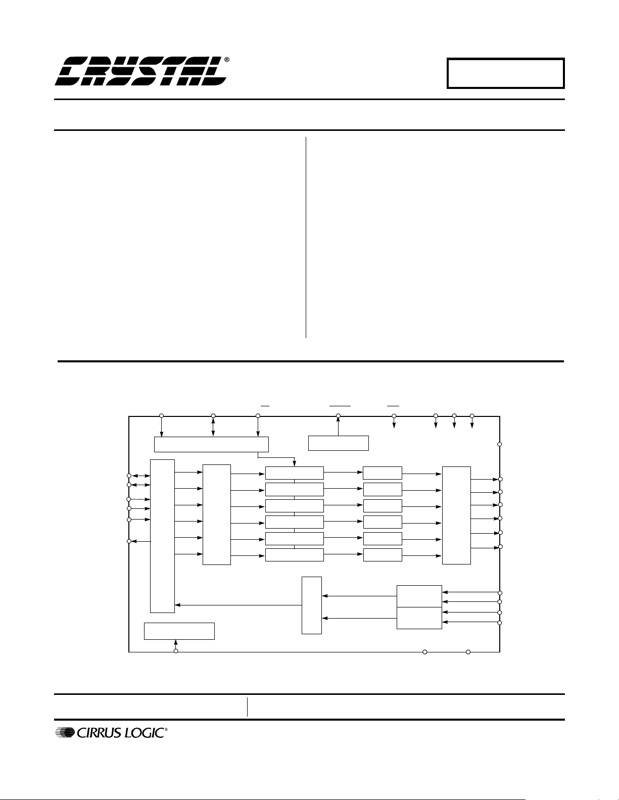
The CS4228 codec provides two analo g-to-digital and
six digital-to-analog delta- sigma converters, along with
volume controls, in a c ompact +5/+3.3 V, 28-pin SSOP
device. Combined with an IEC958 (SPDIF) receiver (like
the CS8414) and surround sound decoder (such as one
of the CS492x or CS493xx families), it is ideal for use in
DVD player, A/V recei ver and car audio systems supporting multiple s tandards such as Dolby Digital A C-3,
AAC, DTS, Dolby ProLogic, THX, and MPEG.
A flexible seri al audio interface allows operation in Left
Justified, Right Justified, I
ORDERING INFORMATION
CS4228-KS -10° to +70° C 28-pin SSOP
CDB4228 Evaluation Board
MUTECAD0/CS
RST
2
S, or One Line Data modes.
VA
VL
CONTROL PORT
LRCK
SCLK
SDIN1
SDIN2
SDIN3
SDOUT
SERIAL AUDIO
DATA INTERFACE
CLOCK MANAGER
MCLK
DIGITAL FILTERS
Advance Product Information
P.O. Box 17847, Austin, Texas 78760
(512) 445 7222 FAX: (512) 445 7581
http://www.cirrus.com
WITH DE-EMPHASIS
DIGITAL VOLUME
DIGITAL VOLUME
DIGITAL VOLUME
DIGITAL VOLUME
DIGITAL VOLUME
DIGITAL VOLUME
MUTE CONTROL
DIGITAL FILTERS
∆Σ
∆Σ
∆Σ
∆Σ
∆Σ
∆Σ
DAC #1
DAC #2
DAC #3
DAC #4
DAC #5
DAC #6
LEFT ADC
RIGHT ADC
DGND
DGND AGND
OUTPUT STAGE
ANALOG LOW PASS AND
AGND
FILT
AOUT1
AOUT2
AOUT3
AOUT4
AOUT5
AOUT6
AINL+
AINL-
AINR+
AINR-
This document contains information for a new product.
Cirrus Logic reserves the right to modify this product without notice.
Copyright Cirrus Logic, Inc. 1999
(All Rights Reserved)
DS307PP1
JUL ‘99
1

TABLE OF CONTENTS
CHARACTERISTICS AND SPECIFICATIONS ................................................... 4
ANALOG CHARACTERISTICS................................................................... 4
DIGITAL CHARACTERISTICS.................................................................... 6
SWITCHING CHARACTERISTICS .................................... ....... ...... ....... ..... 6
SWITCHING CHARACTERISTICS - CONTROL PORT ............................. 8
ABSOLUTE MAXIMUM RATINGS............................................................ 10
RECOMMENDED OPERATING CONDITIONS........................................10
TYPICAL CONNECTION DIAGRAM .................................................................11
FUNCTIONAL DESCRIPTION .......................................................................... 12
Overview ......................... ................................ ................................ ..........12
Analog Inputs ............................................................................................ 12
Line Level Inputs ................................................................................ 12
High Pass Filter ..................................................................................12
Analog Outputs .........................................................................................12
Line Level Outputs ............................................................................. 12
Digital Volume Control .......................................................................13
Mute Control .............................................................................................13
Clock Generation ......................................................................................14
Clock Source ......................................................................................14
Synchronization ........ .......................... ......................... ....................... 14
Digital Interfaces ....................................................................................... 14
Serial Audio Interface Signals ............................................................ 14
Serial Audio Interface Formats ...........................................................14
Control Port Signals ..................................................................................14
SPI Mode ...........................................................................................16
2
I
C Mode ............................................................................................ 16
Control Port Bit Definitions ........................................................................17
Power-up/Reset/Power Down Mode ......................................................... 17
Power Supply, Layout, and Grounding ..................................................... 18
REGISTER DESCRIPTION ................................................................................ 19
PIN DESCRIPTION.............................................................................................24
PARAMETER DEFINITIONS ............................................................................. 28
PACKAGE DIMENSIONS .................................................................................. 29
CS4228
Contacting Cirrus Logic Support
For a complete listing of Direct Sales, Distributor, and Sales Representative contacts, visit the Cirrus Logic web site at:
http://www.cirrus.com/corporate/contacts/
Dolby, Pro Logic, and AC-3 are trademarks of Dolby Laboratories Licensing Corporation.
Preliminary product info rmation describes products which are in production, but for which full characteriza t i on da t a is not yet available. Advance produ ct i nfor-
mation describes products which are in development and subject to development changes. Cirrus Logic, Inc. has made best efforts to ensure that the information
contained in this document is accurate and reli able. However , the i nformati on is sub ject to change with out no tice and i s provi ded “AS IS” withou t warranty of
any kind (express or implied). No responsibility is assumed by Cirrus Logic, Inc. for the use of this information, nor for infringements of patents or other rights
of third parties. This document i s the propert y of Cirru s Logic, Inc. and implie s no licen se under patent s, copyri ghts, trademarks, or tr ade secrets. No part of
this publication may be copied, reproduced , stored in a retrieval system, or transmitted, in any form or by any means (electronic, mechanical, photographic, or
otherwise) without the pri or wri tt en consen t of Ci rrus Logic, Inc. Items from any Cirrus Logi c websi te or disk may be printed for use by the user. However, no
part of the printout or electronic files may be copied, reproduced, stored in a retrieval system, or transmitted, in any form or by any means (electronic, mechanical,
photographic, or otherwise) without the prior written consent of Cirrus Logic, Inc.Furthermore, no part of this publication may be used as a basis for manufacture
or sale of any items without the prior written consent of Cirrus Logic, Inc. The names of products of Cirrus Logic, Inc. or other vendors and suppliers appearing
in this document may be trademarks or service marks of their respective owners which may be registered in some jurisdictions. A list of Cirrus Logic, Inc. trademarks and service marks can be found at http://www.cirrus.com.
2 DS307PP1

LIST OF FIGURES
Figure 1. Serial Audio Port Master Mode Timing ...................................................... 7
Figure 2. Serial Audio Port Slave Mode Timing ........................................................ 7
Figure 3. SPI Control Port Timing ............................................................................. 8
Figure 4. I
Figure 5. Recommended Connection Diagram ....................................................... 11
Figure 6. Optional Line Input Buffer ........................................................................ 12
Figure 7. Passive Output Filter with Mute ............................................................... 13
Figure 8. Butterworth Output Filter with Mute .......................................................... 13
Figure 9. Right Justified Serial Audio Formats ........................................................ 15
Figure 10.I
Figure 11.Left Justified Serial Audio Formats .......................................................... 15
Figure 12.One Line Data Serial Audio Format ......................................................... 16
Figure 13.Control Port Timing, SPI mode ................................................................ 17
Figure 14.Control Port Timing, I
2
2
C Control Port Timing .............................................................................. 9
S Serial Audio Formats .......................................................................... 15
2
C Mode ................................................................. 17
CS4228
DS307PP1 3
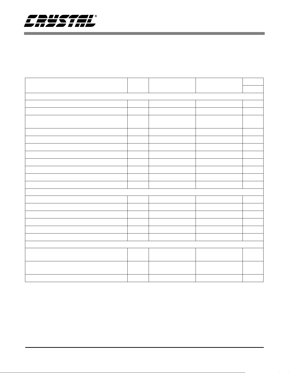
CHARACTERISTICS AND SPECIFICATIONS
CS4228
ANALOG CHARACTERISTICS (Unless otherwise specified T
Full Scale Input Sine wave, 1kHz; Fs = 44.1 kHz BRM, 96 kHz HRM; Measurement Bandwidth is 20 Hz to 20 kHz;
Local components as shown in "Recommended Connection Diagram"; SPI control mode, Left Justified serial format, MCLK = 256 Fs BRM, 128 Fs HRM, SCLK = 64 Fs)
Base Rate Mode High Rate Mode
Parameter Symbol Min Typ Max Min Typ Max Units
Analog Input Characteristics
ADC Resolution Stereo Audio channels
Total Harmonic Distortion
Dynamic Range (A weighted)
Total Harmonic Distortion + Noise -1dB (Note 1)
Interchannel Isolation
Interchannel Gain Mismatch
Offset Error (with high pass filter)
Full Scale Input Voltage (Differential):
Gain Drift
Input Resistance
Input Capacitance
- Minimum gain setting (0 dB) Differential Input; unless otherwise specified.
16 - 24 16 24 Bits
THD - 0.003 - - 0.003 - %
TBD-102
(unweighted)
THD+N - -90 TBD - -90 TBD dB
10--10--k
99
-90- -90- dB
- 0.1 - - 0.1 - dB
--0--0LSB
5.66 5.66 Vp-p
- 100 - - 100 - ppm/°C
- - 15 15 pF
= 25°C; VA = +5V, VD = VL = +3.3V ;
A
-
TBD
-
TBD
102
99
-
-
dB
dB
Ω
A/D Decimation Filter Characteristics
Passband (Note 2)
Passband Ripple
Stopband (Note 2)
Stopband Attenuation (Note 3)
Group Delay (Note 4)
Group Delay Variation vs. Frequency
t
gd
∆
t
0.02 - 20.0 0.02 - 40 kHz
- - 0.01 - - 0.05 dB
27.56 - 5617 66.53 - 5578 kHz
80--45--dB
- 15/Fs - - 15/Fs - s
gd
--0--0µs
High Pass Filter Characteristics
-
Frequency Response: -3 dB (Note 2)
-0.13 dB
Phase Deviation @ 20 Hz
(Note 2)
Passband Ripple
3.4
-
20
-10- -10-Degree
--0--0dB
-
-
-
3.4
-
20
-
-
Hz
Hz
Notes: 1. Referenced to typical full-scale differential input voltage (2 Vrms).
2. Filter characteristics scale with output sample rate.
3. The analog modulator samples the input at 5.6448 MHz for an output sample rate of 44.1 kHz. There is
no rejection of input signals which are multiples of the sampling frequency (n × 5.6448 MHz ±20.0 kHz
where n = 0,1,2,3...).
4. Group delay for Fs = 44.1 kHz, t
Specifications are subject to change without notice
4 DS307PP1
= 15/44.1 kHz = 340µs. Fs = sample rate.
gd
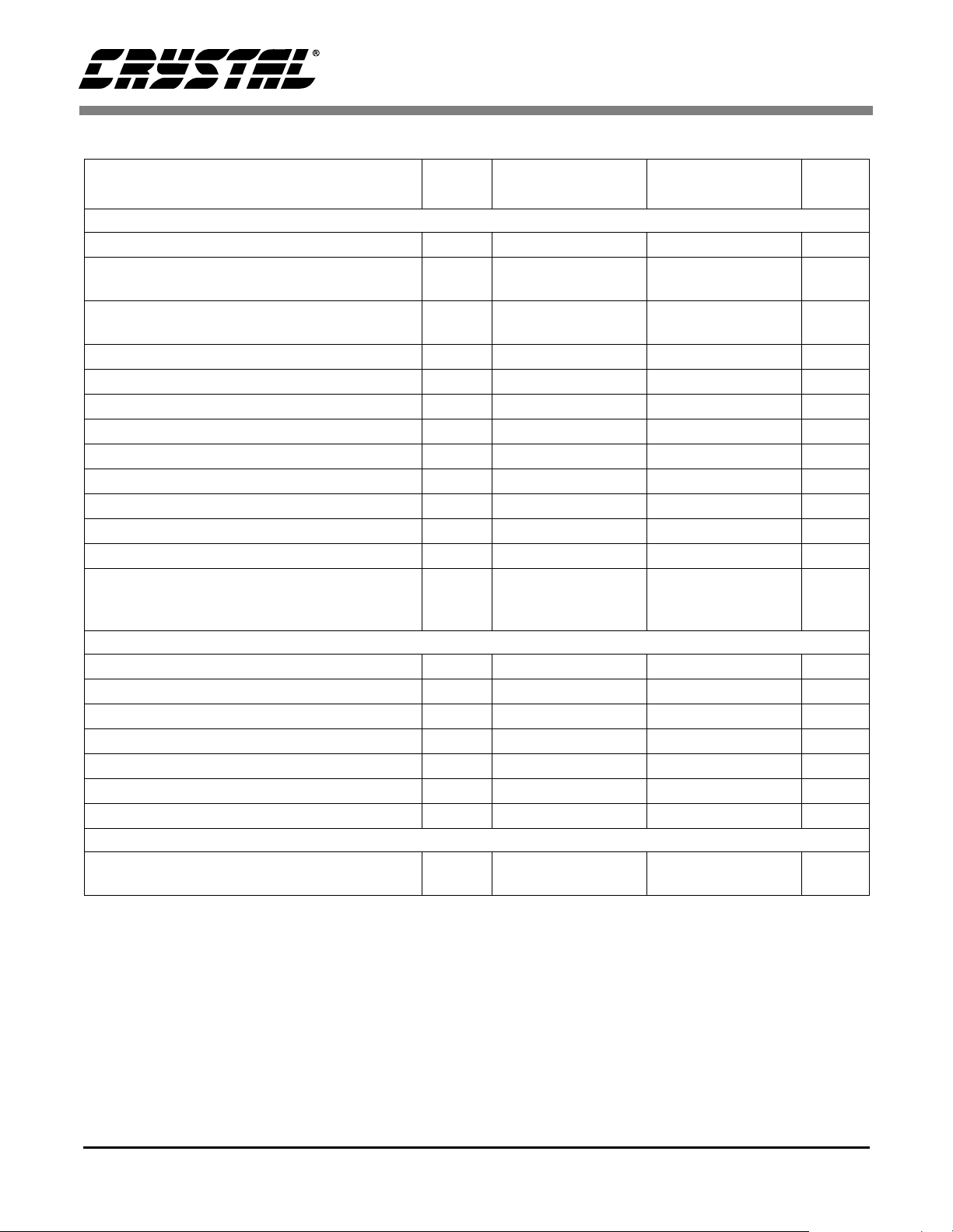
ANALOG CHARACTERISTICS (Continued)
Parameter Symbol Min Typ Max Min Typ Max Units
Analog Output Characteristics
DAC Resolution
Signal-to-Noise/Idle Channel Noise
(DAC muted, A weighted)
Dynamic Range (DAC not muted, A weighted)
(DAC not muted, unweighted)
Total Harmonic Distortion
Total Harmonic Distortion + Noise
Interchannel Isolation
Interchannel Gain Mismatch
Attenuation Step Size (All Outputs)
Programmable Output Attenuation Span
Offset Voltage
Full Scale Output Voltage
Gain Drift
Analog Output Load
Minimum Load Resistance:
Maximum Load Capacitance:
Combined Digital and Analog Filter Characteristics
Frequency Response 10 Hz to 20 kHz
Deviation from Linear Phase
Passband: to 0.01 dB corner (Notes 5, 6)
Passband Ripple (Note 6)
Stopband (Notes 5, 6)
Stopband Attenuation (Notes 4, 7)
Group Delay (Fs = Input Word Rate)
Analog Loopback Performance
Signal-to-noise Ratio
(CCIR-2K weighted, -20 dB FS input)
- Minimum Attenuation, 10 kΩ, 100 pF load; unless otherwise specified.
THD - 0.003 - - 0.003 - %
THD+N - -90 TBD - -90 - dB
tgd - 16/Fs - - 16/Fs - s
CCIR-2K - TBD - - TBD - dB
CS4228
Base Rate Mode High Rate Mode
16 - 24 16 24 Bits
TBD 103 - TBD 103 - dB
TBD-103
100
-90- -90- dB
- 0.1 - - 0.1 - dB
TBD 0.5 TBD TBD 0.5 TBD dB
TBD -90.5 - TBD -90.5 - dB
-10- -10- mV
TBD 1.3 TBD - 1.3 - Vrms
- 100 - - 100 - ppm/°C
-
10
-
100
±0.1 ±0.1 dB
- ±0.5 - - ±0.5 - Degrees
0 - 20.0 0 - 40 kHz
- - ±0.01 - - ±0.01 dB
24.1 - - 56 - - kHz
70--65--dB
-
-
-
-
-
103
-
100
-
10
-
100
-
-
-
-
dB
dB
k
pF
Ω
Notes: 5. The passband and stopband edges scale with frequency. For input word rates, Fs, other than 44.1 kHz,
the 0.01 dB passband edge is 0.4535×Fs and the stopband edge is 0.5465×Fs.
6. Digital filter characteristics.
7. Measurement bandwidth i s 10 Hz to 3 Fs.
Specifications are subject to change without notice
DS307PP1 5
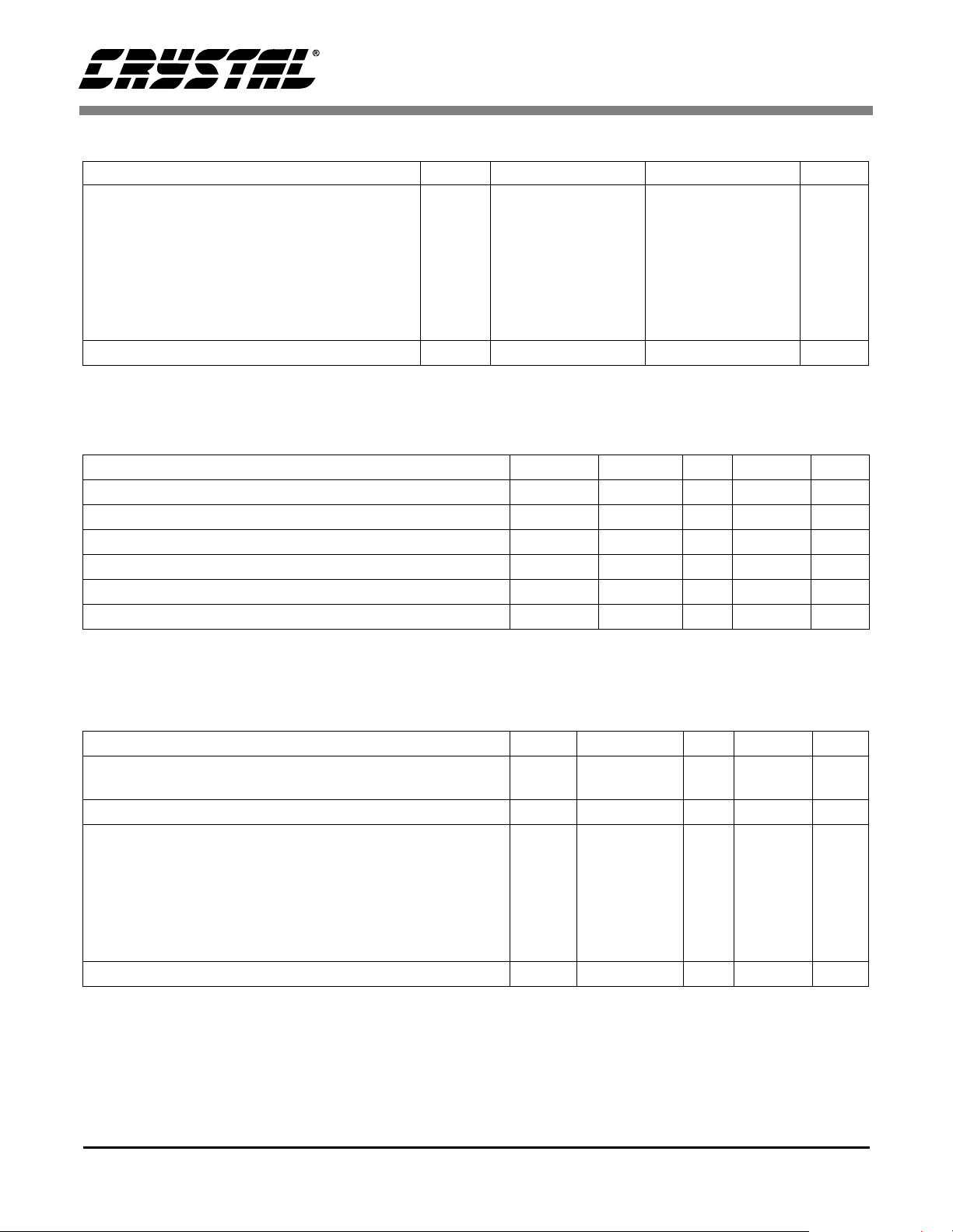
ANALOG CHARACTERISTICS (Continued)
CS4228
Power Supply
Symbol Min Ty p Max Min Typ Max Units
Power Supply Current Operating
25
VA = 5V, VD = VL = 3.3V VA
VL
VD
-
-
-
2
42
Power Down
TBD
-
-
-
2
0.1
- 50 - 50 dB
Power Supply R eje ct i on (1 kH z, 10 mV
VA
VL
VD
rms
)
DIGITAL CHARACTERISTICS Unless otherwise specified (T
VA =+ 5V)
Parameter Symbol Min Typ Max Units
High-level Input Voltage
Low-level Input Voltage
High-level Output Voltage at I
Low-level Output Voltage at I
= -2.0 mA
0
= 2.0 mA
0
Input Leakage Current (Digital Inputs)
Output Leakage Current (High-Impedance Digital Outp uts)
V
IH
V
IL
V
OH
V
OL
TBD
TBD
TBD
TBD
TBD
TBD
= 25 °C; VD = VL = +3.3V;
A
TBD
-
-
-
-
-
2
48
TBD
2
0.1
TBD
TBD
TBD
TBD
TBD
25
0.7xVL - - V
-0.3xVLV
VL - 1.0 - - V
--0.4V
--10µA
--10µA
mA
mA
mA
mA
mA
mA
SWITCHING CHARACTERISTICS (T
= 25°C; VD = VL = +3.3V, VA = +5V, outputs loaded with
A
30 pF)
Parameter Symbol Min Typ Max Units
Audio ADC's & DAC's Sample Rate BRM
HRM
MCLK Frequency
MCLK Duty Cycle BRM
MCLK =128, 384 Fs
MCLK = 256, 512 Fs
HRM
MCLK = 64, 192 Fs
MCLK = 128, 256 Fs
MCLK Jitter Tolerance
Fs 30
60
3.84 - 25.6 MHz
TBD
40
TBD
40
-
-
50
50
-
50
100
TBD
60
TBD
60
kHz
kHz
%
%
%
%
-500-ps
6 DS307PP1
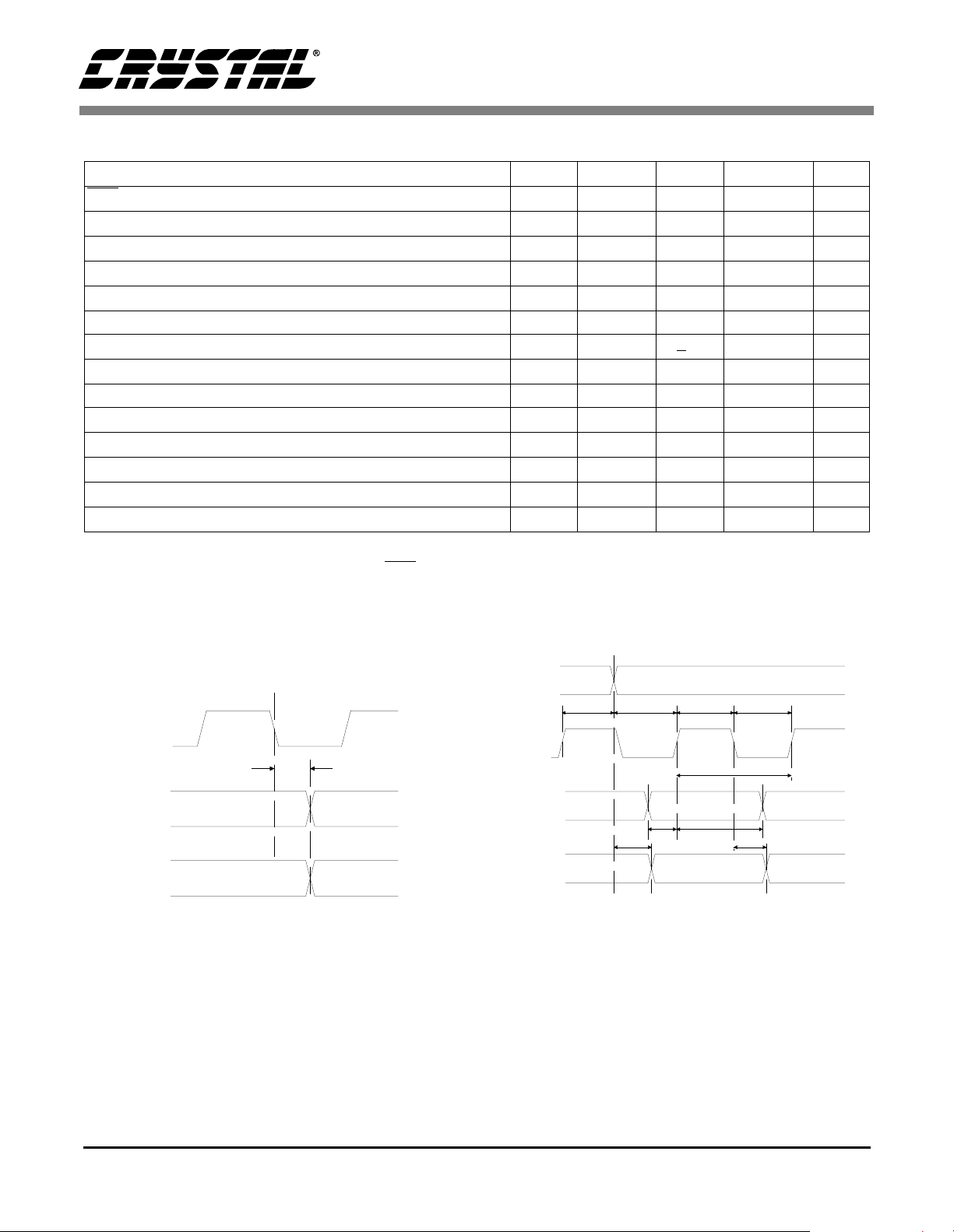
SWITCHING CHARACTERISTICS (Continued)
Figure 1. Serial Audio Port Master Mode Timing
Parameter Symbol Typ Max Units
RST
Low Time (Note 8)
SCLK Falling Edge to SDOUT Output Valid (DSCK=0)
LRCK Edge to MSB Valid
SDIN Setup Time Before SCLK Rising Edge
SDIN Hold Time After SCLK Rising Edge
Master Mode
SCLK Falling to LRCK Edge
SCLK Duty Cycle
Slave Mode
SCLK Period
SCLK High Time
SCLK Low Time
SCLK rising to LRCK Edge (DSCK=0)
LRCK Edge to SCLK Rising (DSCK=0)
t
dpd
t
lrpd
t
t
t
mslr
t
sckw
t
sckh
t
sckl
t
lrckd
t
lrcks
ds
dh
CS4228
1- -ms
-TBDns
-TBDns
-TBDns
-TBDns
+10 - ns
50 - %
--ns
TBD - - ns
TBD - - ns
TBD - - ns
TBD - - ns
Notes: 8. After powering up the CS4228, RST
SCLK*
(output)
t
mslr
LRCK
(output)
SDOUT
should be held low until the power supplies and clocks are settled.
LRCK
(input)
SCLK*
(input)
SDIN1
SDIN2
SDIN3
SDOUT
*SCLK shown for DSCK = 0.
SCLK inverted for DSCK = 1.
t
lrckd
t
lrpd
t
lrcks
t
sckh
t
t
ds
dh
MSB
t
sckw
t
sckl
t
dpd
MSB-1
Figure 2. Serial Audio Port Slave Mo de Timing
DS307PP1 7
CS4228
SWITCHING CHARACTERISTICS - CONTROL PORT (TA = 25°C, VD = VL = +3.3V,
VA = +5V; Inputs: logic 0 = DGND, logic 1 = VL+, C
Parameter Symbol Min Max Units
SPI Mode
(SDOUT > 47kΩ to GND)
CCLK Clock Frequency
High Time Between Transmissions
CS
CS
Falling to CCLK Edge
CCLK Low Time
CCLK High Time
CDIN to CCLK Rising Setup Time
CCLK Rising to DATA Hold Time (Note 9)
Rise Time of CCLK and CDIN (Note 10)
Fall Time of CCLK and CDIN (Note 10)
Notes: 9. Data must be held for sufficient time to bridge the transition time of CCLK.
10. For F
SCK
< 1 MHz
= 30 pF)
L
f
t
t
t
t
sck
csh
css
t
scl
sch
dsu
t
dh
t
t
-6MHz
1.0
20 ns
66 ns
66 ns
40 ns
15 ns
r2
f2
100 ns
100 ns
µ
s
CS
CCLK
CDIN
t
css
t
r2
t
t
scl
t
t
f2
dsu
sch
t
dh
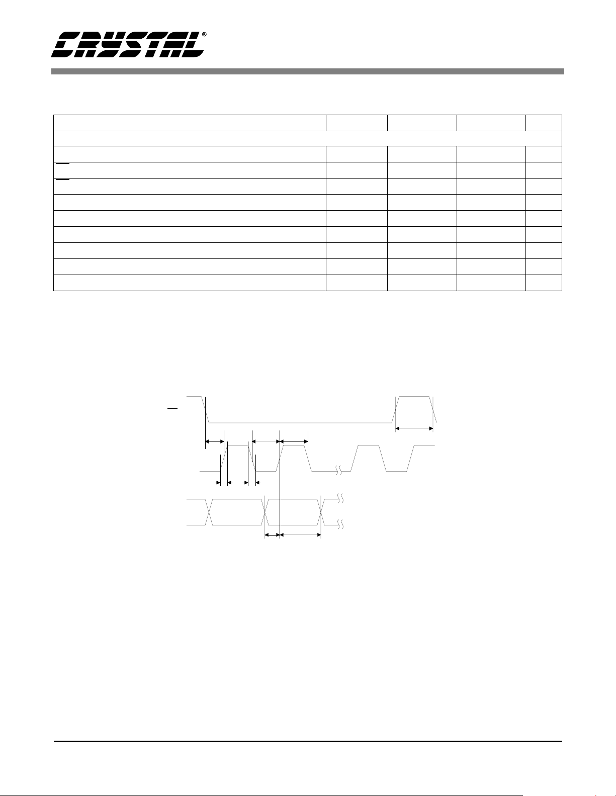
Figure 3. SPI Control Port Timing
t
csh
8 DS307PP1
CS4228
SWITCHING CHARACTERISTICS - CONTROL PORT (T
VA = +5V; Inputs: logic 0 = DGND, logic 1 = VL, C
Parameter Symbol Min Max Units
I2C® Mode
(SDOUT < 47kΩ to ground) (Note 11)
SCL Clock Frequency
Bus Free Time Between Transmissions
Start Condition Hold Time (prior to first clock pulse)
Clock Low Time
Clock High Time
Setup Time for Repeated Start Condition
SDA Hold Time from SCL Falling (Note 12)
SDA Setup Time to SCL Rising
Rise Time of Both SDA and SCL Lines
Fall Time of Both SDA and SCL Lines
Setup Time for Stop Condition
Notes: 11. Use of the I
2
C bus interface requires a license from Philips. I2C is a registered trademark of Philips
Semiconductors.
12. Data must be held for sufficient time to bridge the 300 ns transition time of SCL.
= 30 pF)
L
f
t
buf
t
hdst
t
low
t
high
t
sust
t
hdd
t
sud
t
susp
scl
t
t
r
f
= 25°C; VD = VL = +3.3V,
A
-100kHz
4.7
4.0
4.7
4.0
4.7
0
µ
s
µ
s
µ
s
µ
s
µ
s
µ
s
250 ns
1
µ
s
300 ns
4.7
µ
s
SDA
SCL
Stop Start
t
buf
t
hdst
t
low
Repeated
Start
t
high
t
hdd
t
sud
t
sust
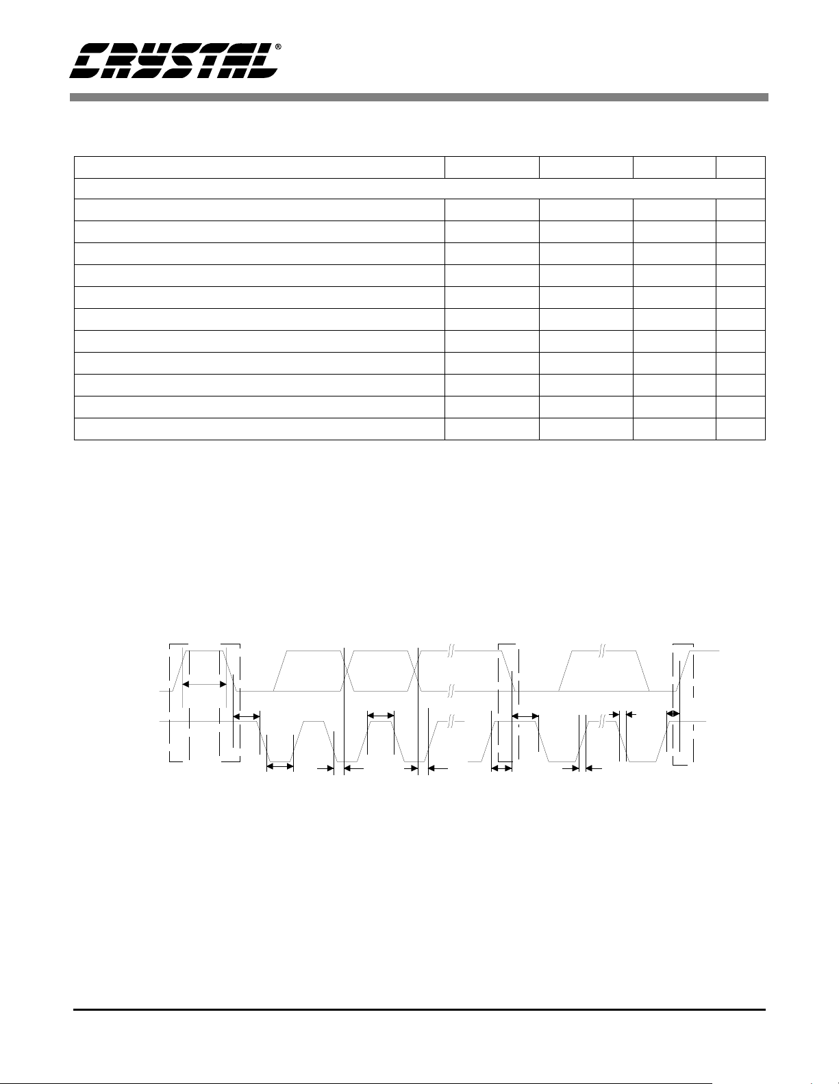
Figure 4. I2C Control Port Timing
t
hdst
Stop
t
f
t
r
t
susp
DS307PP1 9
 Loading...