

CS4228A
24-Bit, 96 kHz Surround Sound Codec
Features
! Six 24-bit D/A converters
- 100 dB dynamic range
- -90 dB THD+N
! Two 24-bit A/D converters
- 97 dB dynamic range
- -88 dB THD+N
! Sampleratesupto100kHz
! Pop-free digital output volume controls
- 90.5 dB range, 0.5 dB resolution (182 levels)
- Variable smooth ramp rate, 0.125 dB steps
! Mute control pin for off-chip muting circuits
! On-chip anti-alias and output filters
! De-emphasis filters for 32, 44.1 and 48 kHz
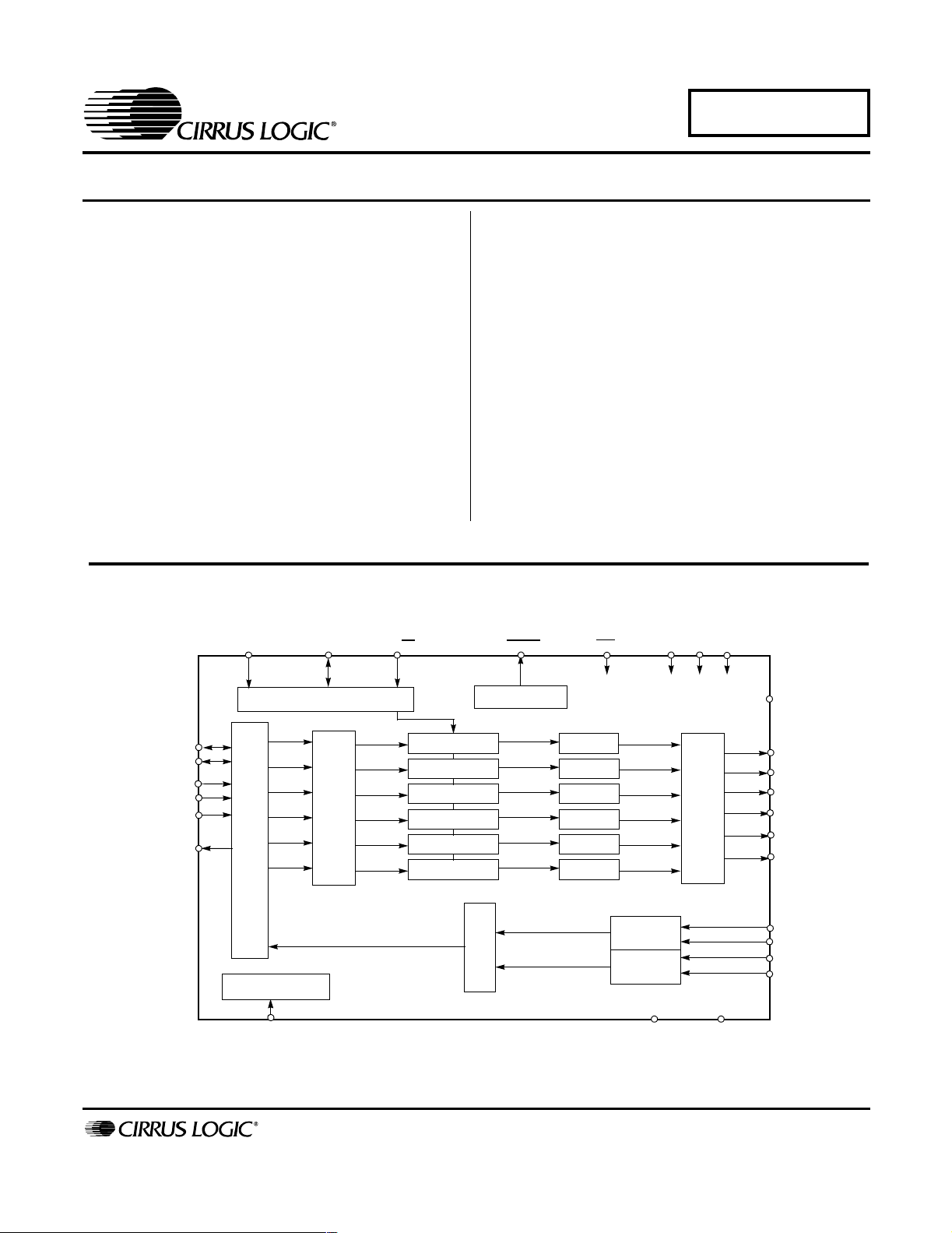
I
SCL/CCLK SDA/CDIN VD
AD0/CS
Description
The CS4228A codec provides two analog-to-digital and
six digital-to-analog Delta-Sigma converters, along with
volume controls, in a compact 28-pin SSOP device.
Combined with an IEC958 (SPDIF) receiver (like the
CS8414) and surround sound decoder (such as one of
the CS492x or CS493xx families), it is ideal for use in
DVD player, A/V receiver and car audio systems supporting multiple standards such as Dolby Digital AC-3
AAC
,DTS, Dolby ProLogic,THX, and other
multi-channel formats.
A flexible serial audio interface allows operation in Left
Justified, Right Justified, I
2
S, or One Line Data modes.
ORDERING INFORMATION
CS4228A-KS
-10° to +70°C 28-pin SSOP
CDB4228A Evaluation Board
MUTEC
RST
VA
VL
,
LRCK
SCLK
SDIN1
SDIN2
SDIN3
SDOUT
www.cirrus.com
CONTROL PORT
SERIAL AUDIO
DATA INTERFACE
CLOCK MANAGER
MCLK
MUTE CONTROL
DIGITAL VOLUME
DIGITAL VOLUME
DIGITAL VOLUME
DIGITAL VOLUME
DIGITAL FILTERS
WITH DE-EMPHASIS
DIGITAL VOLUME
DIGITAL VOLUME
DIGITAL FILTERS
Copyright Cirrus Logic, Inc. 2003
(All Rights Reserved)
∆Σ
∆Σ
∆Σ
∆Σ
∆Σ
∆Σ
DAC #1
DAC #2
DAC #3
DAC #4
DAC #5
DAC #6
LEFT ADC
RIGHT ADC
DGND
OUTPUT STAGE
ANALOG LOW PASS AND
AGND
FILT
FL
FR
SL
SR
CENTER
SUB
AINL+
AINL-
AINR+
AINR-
MAR ‘03
DS511F1
1

TABLE OF CONTENTS
1. CHARACTERISTICS AND SPECIFICATIONS ........................................................................ 4
SPECIFIED OPERATING CONDITIONS ................................................................................. 4
ABSOLUTE MAXIMUM RATINGS ........................................................................................... 4
ANALOG CHARACTERISTICS ................................................................................................ 5
POWER AND THERMAL CHARACTERISTICS....................................................................... 7
DIGITAL CHARACTERISTICS ................................................................................................. 7
SWITCHING CHARACTERISTICS .......................................................................................... 8
SWITCHING CHARACTERISTICS - CONTROL PORT......................................................... 10
2. TYPICAL CONNECTION DIAGRAM ...................................................................................... 12
3. FUNCTIONAL DESCRIPTION ............................................................................................... 13
3.1 Overview .......................................................................................................................... 13
3.2 Analog Inputs ................................................................................................................... 13
3.2.1 Line Level Inputs ................................................................................................. 13
3.2.2 High Pass Filter ................................................................................................... 13
3.3 Analog Outputs ................................................................................................................14
3.3.1 Line Level Outputs .............................................................................................. 14
3.3.2 Digital Volume Control ........................................................................................ 14
3.4 Mute Control .................................................................................................................... 15
3.5 Clock Generation ............................................................................................................. 15
3.5.1 Clock Source ....................................................................................................... 15
3.5.2 Synchronization ................................................................................................... 15
3.6 Digital Interfaces .............................................................................................................. 15
3.6.1 Serial Audio Interface Signals ............................................................................. 15
3.6.2 Serial Audio Interface Formats ............................................................................ 16
CS4228A
Contacting Cirrus Logic Support
For all product questions and inquiries contact a Cirrus Logic Sales Representative.
To find one nearest you go to www.cirrus.com
IMPORTANT NOTICE
Cirrus Logic, Inc. and its subsidiaries ("Cirrus") believe that the information contained in this document is accurate and reliable. However, the information is subject
to change without notice and is provided "AS IS" without warranty of any kind (express or implied). Customers are advised to obtain the latest version of relevant
information to verify, before placing orders, that information being relied on is current and complete. All products are sold subject to the terms and conditions of
sale supplied at the time of order acknowledgment, including those pertaining to warranty, patent infringement, and limitation of liability. No responsibility is assumed by Cirrus for the use of this information, including use of this information as the basis for manufacture or sale of any items, or for infringement of patents or
other rights of third parties. This document is the property of Cirrus and by furnishing this information, Cirrus grants no license, express or implied under any patents,
mask work rights, copyrights, trademarks, trade secrets or other intellectual property rights. Cirrus owns the copyrights associated with the information contained
herein and gives consent for copies to be made of the information only for use within your organization with respect to Cirrus integrated circuits or other parts of
Cirrus. This consent does not extend to other copying such as copying for general distribution, advertising or promotional purposes, or for creating any work for
resale.
An export permit needs to be obtained from the competent authorities of the Japanese Government if any of the products or technologies described in this material
and controlled under the "Foreign Exchange and Foreign Trade Law" is to be exported or taken out of Japan. An export license and/or quota needs to be obtained
from the competent authorities of the Chinese Government if any of the products or technologies described in this material is subject to the PRC ForeignTrade
Law and is to be exported or taken out of the PRC.
CERTAIN APPLICATIONS USING SEMICONDUCTOR PRODUCTS MAY INVOLVE POTENTIAL RISKS OF DEATH, PERSONAL INJURY, OR SEVERE PROPERTY OR ENVIRONMENTAL DAMAGE ("CRITICAL APPLICATIONS"). CIRRUS PRODUCTS ARE NOT DESIGNED, AUTHORIZED OR WARRANTED FOR
USE IN AIRCRAFT SYSTEMS, MILITARY APPLICATIONS, PRODUCTS SURGICALLY IMPLANTED INTO THE BODY, LIFE SUPPORT PRODUCTS OR OTHER CRITICAL APPLICATIONS (INCLUDING MEDICAL DEVICES, AIRCRAFT SYSTEMS OR COMPONENTS AND PERSONAL OR AUTOMOTIVE SAFETY
OR SECURITY DEVICES). INCLUSION OF CIRRUS PRODUCTS IN SUCH APPLICATIONS IS UNDERSTOOD TO BE FULLY AT THE CUSTOMER'S RISK
AND CIRRUS DISCLAIMS AND MAKES NO WARRANTY, EXPRESS, STATUTORY OR IMPLIED, INCLUDING THE IMPLIED WARRANTIES OF MERCHANTABILITY AND FITNESS FOR PARTICULAR PURPOSE, WITH REGARD TO ANY CIRRUS PRODUCT THAT IS USED IN SUCH A MANNER. IF THE CUSTOMER OR CUSTOMER'S CUSTOMER USES OR PERMITS THE USE OF CIRRUS PRODUCTS IN CRITICAL APPLICATIONS, CUSTOMER AGREES, BY SUCH
USE, TO FULLY INDEMNIFY CIRRUS, ITS OFFICERS, DIRECTORS, EMPLOYEES, DISTRIBUTORS AND OTHER AGENTS FROM ANY AND ALL LIABILITY,
INCLUDING ATTORNEYS' FEES AND COSTS, THAT MAY RESULT FROM OR ARISE IN CONNECTION WITH THESE USES.
Cirrus Logic, Cirrus, and the Cirrus Logic logo designs are trademarks of Cirrus Logic, Inc. All other brand and product names in this document may be trademarks
or service marks of their respective owners.
2
C is a registered trademark of Philips Semiconductor. Purchase of I2C Components of Cirrus Logic, Inc., or one of its sublicensed Associated Companies conveys
I
a license under the Philips I
DTS is a registered trademark of the Digital Theater Systems, Inc.
Dolby, Dolby Digital, AC-3, AAC, and Pro Logic are registered trademarks of Dolby Laboratories, Inc.
THX is a registered trademark of Lucasfilms Ltd.
2
C Patent Rights to use those components in a standard I2C system.
2

CS4228A
3.7 Control Port Signals ......................................................................................................... 18
3.7.1 SPI Mode ............................................................................................................ 18
3.7.2 I2C Mode ............................................................................................................ 18
3.8 Control Port Bit Definitions .............................................................................................. 19
3.9 Power-up/Reset/Power Down Mode ............................................................................... 19
3.10 Power Supply, Layout, and Grounding .......................................................................... 20
4. REGISTER QUICK REFERENCE .......................................................................................... 21
5. REGISTER DESCRIPTIONS .................................................................................................. 22
5.1 Memory Address Pointer (MAP) ..................................................................................... 22
5.2 CODEC Clock Mode ........................................................................................................ 22
5.3 Chip Control ..................................................................................................................... 22
5.4 ADC Control .................................................................................................................... 23
5.5 DAC Mute1 Control ......................................................................................................... 23
5.6 DAC Mute2 Control ......................................................................................................... 24
5.7 DAC De-emphasis Control .............................................................................................. 24
5.8 Digital Volume Control ..................................................................................................... 24
5.9 Serial Port Mode .............................................................................................................. 25
5.10 Chip Status .................................................................................................................... 25
6. PIN DESCRIPTION ................................................................................................................. 26
7. PARAMETER DEFINITIONS .................................................................................................. 29
8. PACKAGE DIMENSIONS ...................................................................................................... 31
LIST OF FIGURES
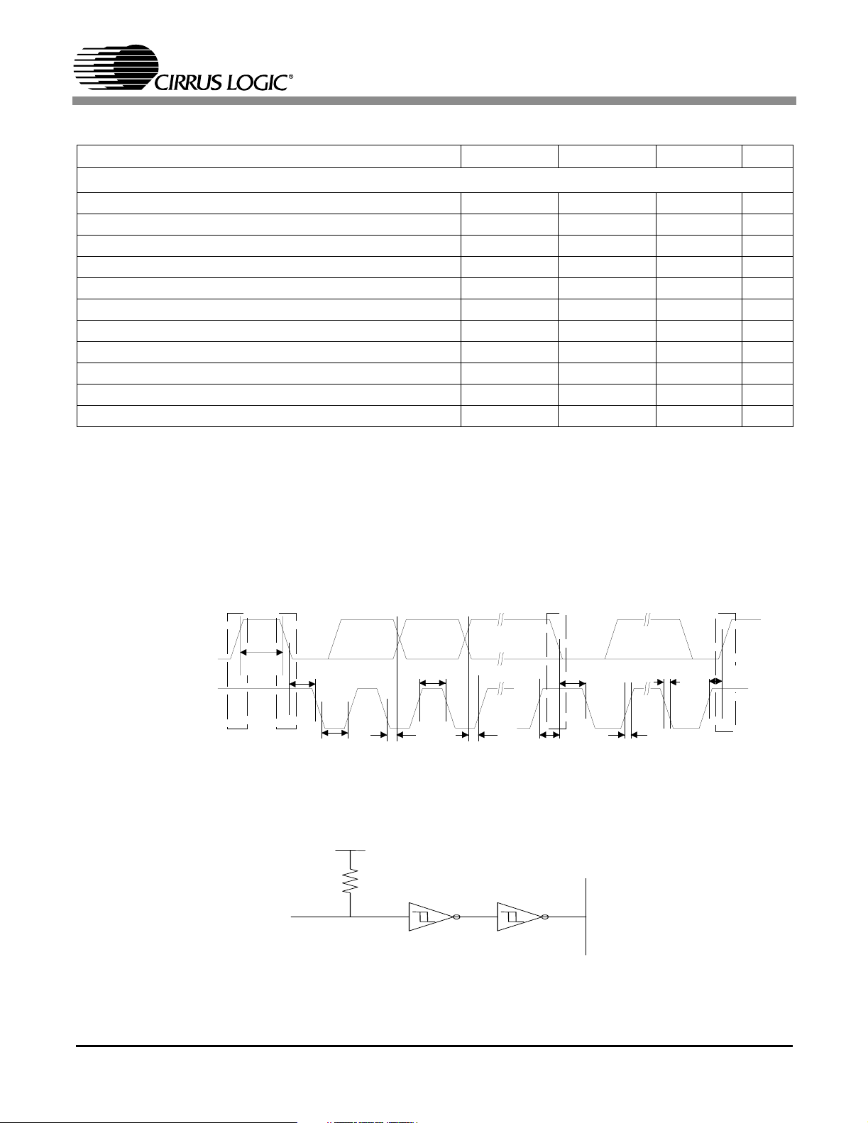
Figure 1. Serial Audio Port Master Mode Timing ............................................................................ 9
Figure 2. Serial Audio Port Slave Mode Timing .............................................................................. 9
Figure 3. SPI Control Port Timing ................................................................................................. 10
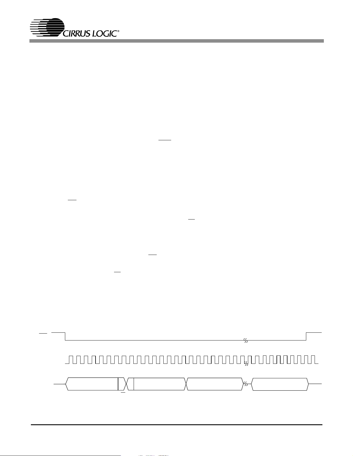
Figure 4. I2C Control Port Timing ................................................................................................. 11
Figure 5. I2C Mode SCL Buffer Example...................................................................................... 11
Figure 6. Recommended Connection Diagram............................................................................. 12
Figure 7. Optional Line Input Buffer .............................................................................................. 13
Figure 8. Passive Output Filter with Mute ..................................................................................... 14
Figure 9. Butterworth Output Filter with Mute ............................................................................... 14
Figure 10. I
Figure 11. Left Justified Serial Audio Formats .............................................................................. 16
Figure 12. Right Justified Serial Audio Formats ............................................................................ 17
Figure 13. One Line Data Serial Audio Format ............................................................................. 17
Figure 14. Control Port Timing, SPI Slave Mode Write................................................................. 18
Figure 15. Control Port Timing, I2C Slave Mode Write ................................................................. 19
Figure 16. Control Port Timing, I2C Slave Mode Read................................................................. 19
2
S Serial Audio Formats ............................................................................................. 16
LIST OF TABLES
Table 1. Serial Audio Port Input Channel Allocations ................................................................... 16
Table 2. User Registers ................................................................................................................ 21
Table 3. Common Master Clock Frequencies.............................................................................. 27
3
CS4228A
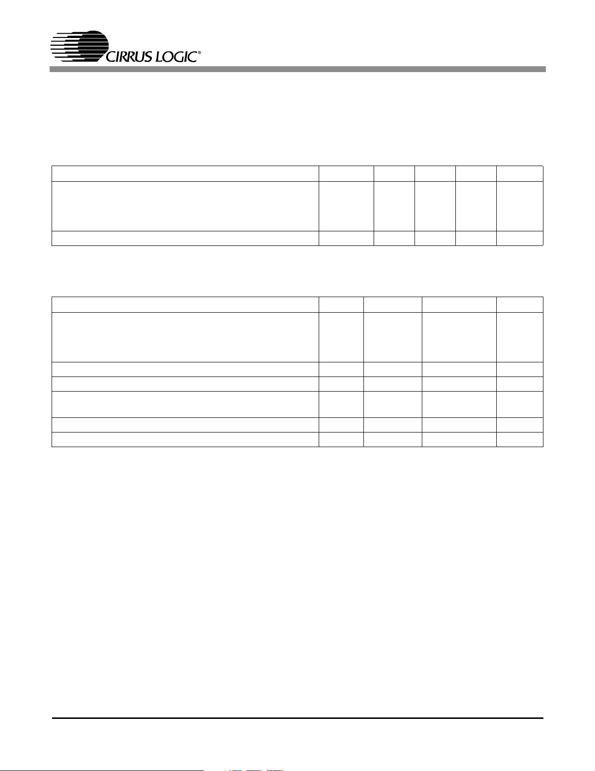
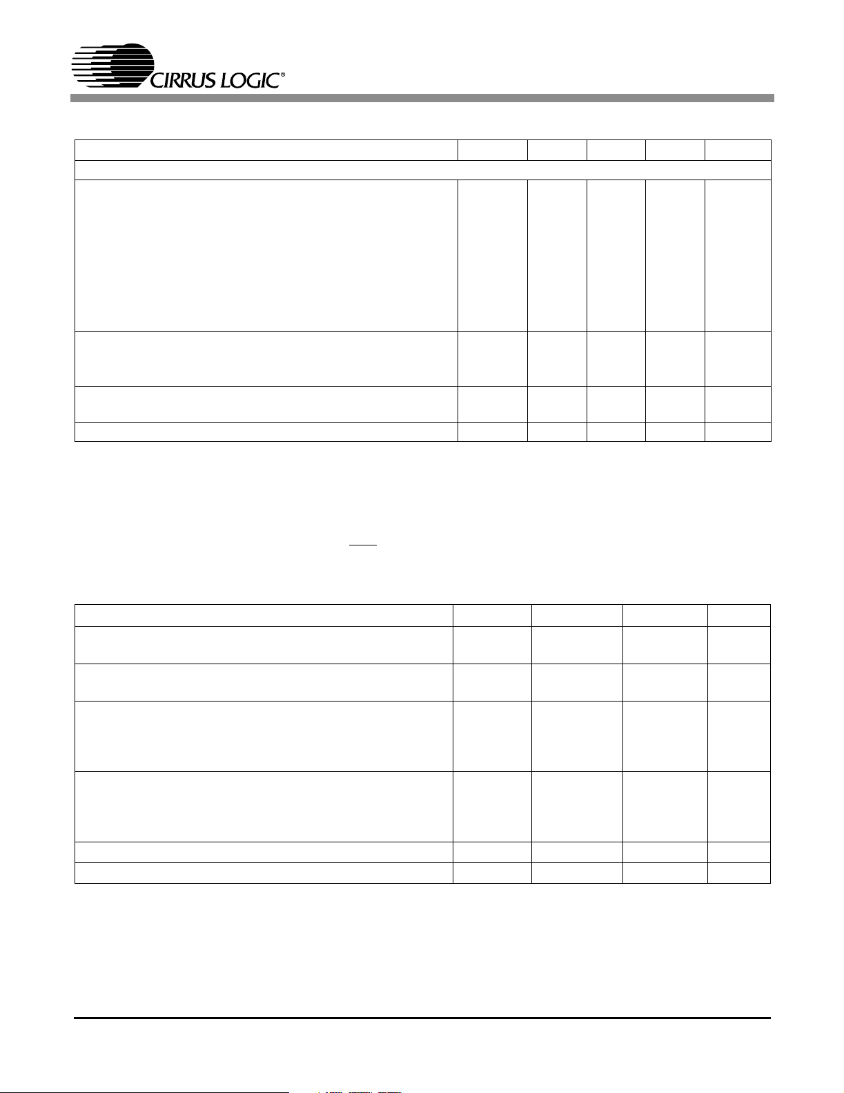
1. CHARACTERISTICS AND SPECIFICATIONS
(Min/Max performance characteristics and specifications are guaranteed over the Specified Operating Conditions.
Typical performance characteristics are derived from measurements taken at T
SPECIFIED OPERATING CONDITIONS ((AGND, DGND = 0V; all voltages with respect to
ground.)
Parameter Symbol Min Typ Max Units
DC Power Supply Digital
Analog
Interface
VD - VL (Note 12)
Specified Temperature Range (-KS) T
VD
VA
VL
A
ABSOLUTE MAXIMUM RATINGS (AGND, DGND = 0 V, all voltages with respect to ground.)
Parameter Symbol Min Max Units
DC Power Supply Digital
Analog
Interface
VD - VL
Input Current (Note 1) - ±10 mA
Analog Input Voltage (Note 2) -0.7 VA + 0.7 V
Digital Input Voltage Input Pins
Bidirectional Pins (Notes 2 and 3)
Ambient Temperature (Power Applied) -55 +125 °C
Storage Temperature -65 +150 °C
VD
VA
VL
=25°C, VA = 5.0V, VD = 5.0V)
A
4.75
4.75
3.0*
-
-10 - 70 °C
-0.3
-0.3
-0.3
-
-0.7
-0.7
5.0
5.0
-
-
5.25
5.25
5.25
2.00
6.0
6.0
6.0
2.0
VL + 2.5
VL + 0.7
V
V
V
V
V
V
V
V
V
V
Notes: 1. Any pin except supplies. Transient currents of up to ±100 mA on the analog input pins will not cause
SCR latch-up.
2. The maximum over or under voltage is limited by the input current.
3. Bidirectional pins configured as inputs.
Warning: Operation at or beyond these limits may result in permanent damage to the device. Normal operation
is not guaranteed at these extremes.
4
CS4228A
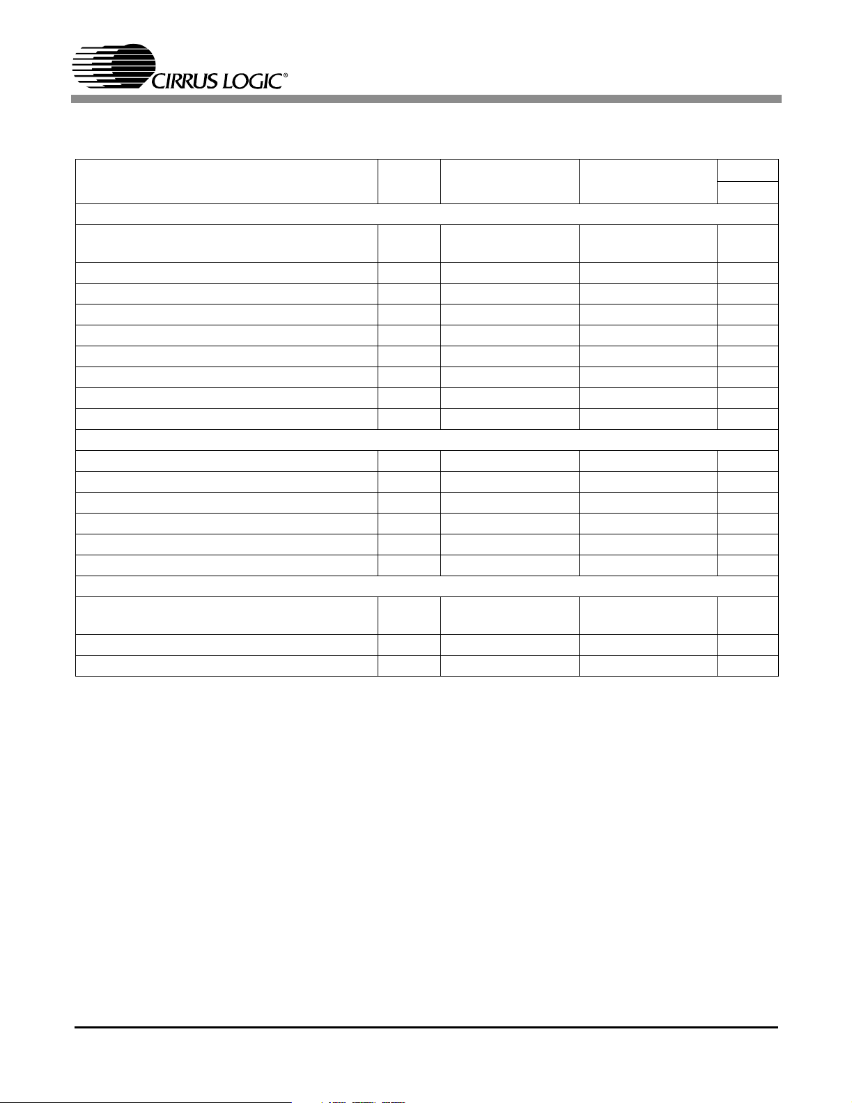
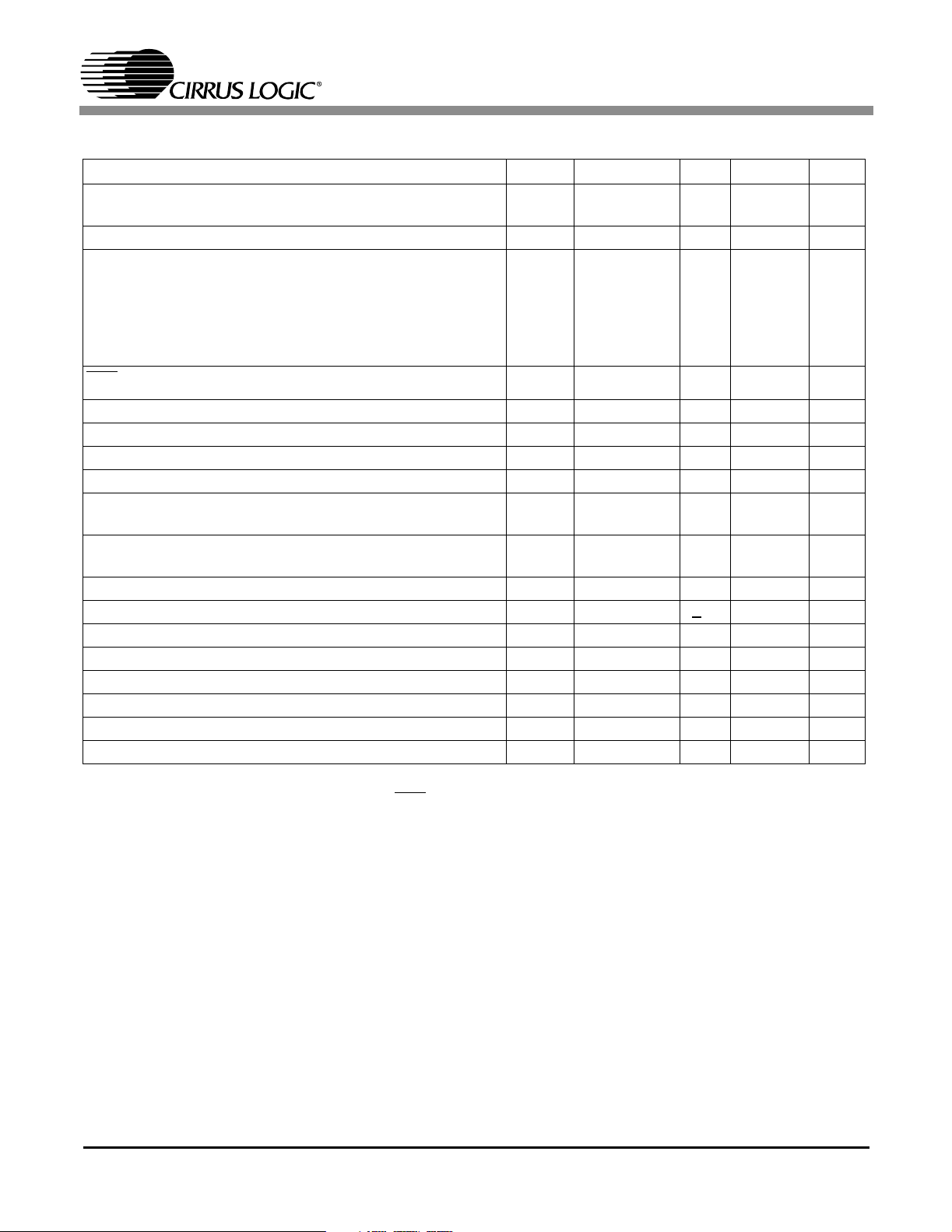
ANALOG CHARACTERISTICS (Test conditions (unless otherwise specified): Input test signal is a
997 Hz sine wave at 0 dBFS; measurement bandwidth is 10 Hz to 20 kHz; test load R
Base Rate Mode High Rate Mode
Parameter Symbol Min Typ Max Min Typ Max Units
Analog Input Characteristics - Minimum gain setting (0 dB) Differential Input; unless otherwise specified.
Dynamic Range, -60 dBFS input (A weighted)
(unweighted)
Total Harmonic Distortion + Noise (Note 4) THD+N - -88 -83 - -88 -83 dB
Interchannel Isolation - 100 - - 100 - dB
Interchannel Gain Mismatch - 0.1 - - 0.1 - dB
Offset Error (with high pass filter) - - 0 - - 0 LSB
Full Scale Input Voltage (Differential): 5.24 5.66 6.09 5.24 5.66 6.09 Vp-p
Gain Drift - 100 - - 100 - ppm/°C
Input Resistance 10 - - 10 - - kΩ
Input Capacitance - - 15 - - 15 pF
A/D Decimation Filter Characteristics
Passband (Note 5) 0.022 - 21.77 0.022 - 43.54 kHz
Passband Ripple - - 0.01 - - 0.05 dB
Stopband (Note 5) 30.0 - 6114 72.41 - 6071 kHz
Stopband Attenuation (Note 6) 80 - - 45 - - dB
Group Delay t
Group Delay Variation vs. Frequency ∆ t
High Pass Filter Characteristics
Frequency Response: -3 dB (Note 7)
-0.13 dB
Phase Deviation @ 20 Hz (Note 7) - 10 - - 10 - Degree
Passband Ripple - - 0 - - 0 dB
gd
gd
91 97
94
- 17/Fs - - 17/Fs - s
--0--0µs
-
3.4
-
20
-
-
-
-
=10kΩ,CL=15pF)
L
91 97
94
-
3.4
-
20
-
-
-
-
dB
dB
Hz
Hz
Notes: 4. Referenced to typical full-scale differential input voltage (2 Vrms). Tested at -1 dBFS
5. Filter characteristics scale with output sample rate.
6. The analog modulator samples the input at 128 times Fs. For example, to obtain an output sample rate
of 48 kHz the input must be sampled at 6.144 MHz. There is no rejection of input signals which are
multiples of the sampling frequency (n × 6.144 MHz ±20.0 kHz where n = 0,1,2,3...).
7. High Pass Filter characteristics are specified for Fs=44.1 kHz.
5
CS4228A
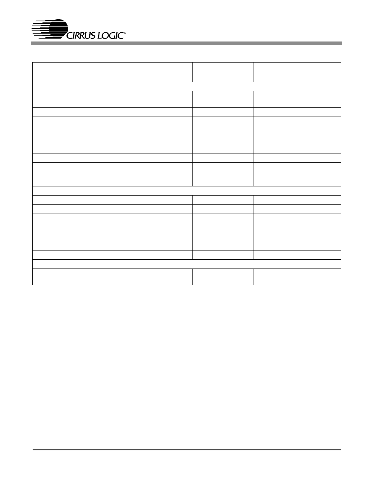
ANALOG CHARACTERISTICS (Continued)
Base Rate Mode High Rate Mode
Parameter Symbol Min Typ Max Min Typ Max Units
Analog Output Characteristics - Minimum Attenuation, 10 kΩ, 10 pF load; unless otherwise specified.
Dynamic Range, -60 dBFS input (A weighted)
(unweighted)
Total Harmonic Distortion + Noise (unweighted) THD+N - -90 -83 - -90 -83 dB
Interchannel Isolation - 95 - - 95 - dB
Interchannel Gain Mismatch - 0.1 - - 0.1 - dB
Offset Voltage - 10 - - 10 - mV
Full Scale Output Voltage 3.42 3.7 3.98 3.42 3.7 3.98 Vp-p
Gain Drift - 100 - - 100 - ppm/°C
Analog Output Load
Minimum Load Resistance:
Maximum Load Capacitance:
Combined Digital and Analog Filter Characteristics
Frequency Response 10 Hz to 20 kHz ±0.1 ±0.1 dB
Deviation from Linear Phase - ±0.5 - - ±0.5 - Degrees
Passband: to 0.01 dB corner (Notes 8, 9) 0 - 21.77 0 - 43.54 kHz
Passband Ripple (Note 9) - - ±0.01 - - ±0.01 dB
Stopband (Notes 8, 9) 26.2 - - 62.5 - - kHz
Stopband Attenuation (Notes 8, 10) 70 - - 65 - - dB
Group Delay (Fs = Input Word Rate) tgd - 29/Fs - - 17/Fs - s
Analog Loopback Performance
Signal-to-noise Ratio
(CCIR-2K weighted, -20 dB FS input)
CCIR-2K - 90 - - 90 - dB
93-100
97
-
10
-
100
-
-
-
-
93-100
97
-
10
-
100
-
-
-
-
dB
dB
kΩ
pF
8. The passband and stopband edges scale with frequency. For input word rates, Fs, other than 44.1 kHz,
the 0.01 dB passband edge is 0.4535×Fs and the stopband edge is 0.5465×Fs.
9. Digital filter characteristics.
10. Measurement bandwidth is 10 Hz to 3 Fs.
6
POWER AND THERMAL CHARACTERISTICS
Parameters Symbol Min Typ Max Units
Power Supplies
Power Supply Current normal operation, V
A=VD=VL
(Note 11, Note 12) BRM
power-down state (all supplies) (Note 13)
Power Dissipation (Note 11)
V
A=VD=VL
= 5V normal operation
power-down (Note 13)
Package Thermal Resistance TSSOP (-KS) θ
Power Supply Rejection Ratio (1 kHz, 10 mV
=5V
BRM
)PSRR - 50 - dB
rms
CS4228A
I
A
I
D
I
L
I
A
I
D
I
L
-
-
-
-
-
-
-
-
JA
θ
JC
-
-
35
78
0.3
0.2
0.4
0.2
567
4
56
37
42
105
2
1
15
0.5
715
12.5
-
-
mA
mA
mA
mA
mA
mA
mW
mW
°C/Watt
°C/Watt
Notes: 11. Current consumption increases with increasing FS and increasing MCLK. Variance between speed
modesissmall.
12. VD current consumption increases (ID normal and ID_pdn) when VD - VL > 1.5V. When VD - VL = 1.7V,
typically increases by 2 mA and when VD - VL = 2V, IDtypically increases by 12 mA.
I
D
13. Power down mode is defined as RST
pin = Low with clocks running.
DIGITAL CHARACTERISTICS (AGND, DGND = 0V, all voltages with respect to ground.)
Parameter Symbol Min Max Units
High-level Input Voltage VL=5V
Low-level Input Voltage
High-level Input Voltage VL=3.3V
Low-level Input Voltage
High-level Output Voltage at
VL = 5V I
VL = 3.3V I
=-2.0mA
0
I
= -100 µA
0
=-2.0mA
0
Low-level Output Voltage at
VL = 5V I
VL = 3.3V I
=2.0mA
0
I
= 100 µA
0
=-2.0mA
0
Input Leakage Current (Digital Inputs) - 10 µA
Output Leakage Current (High-Impedance Digital Outputs) - 10 µA
V
IH
V
IL
V
IH
V
IL
V
OH
V
OH
V
OH
V
OL
V
OL
V
OL
0.7 x VL
-
2.2
-
VL - 1.0
VL - 0.7
2.3
-
-
-
-
0.3 x VL
-
1.0
-
-
-
0.4
0.2
0.4
V
V
V
V
V
V
V
V
V
V
7
CS4228A
SWITCHING CHARACTERISTICS (Inputs: Logic 0 = 0V, Logic 1 = VL)
Parameter Symbol Min Typ Max Units
Audio ADC's and DAC's Sample Rate BRM
HRM
MCLK Frequency (Note 14) 3.84 - 25.6 MHz
MCLK Duty Cycle BRM
MCLK =128, 384 Fs
MCLK = 256, 512 Fs
HRM
MCLK = 64, 192 Fs
MCLK = 128, 256 Fs
RST
Low Time (Note 15)
Fs 30
60
40
40
40
40
1--ms
50
50
50
50
-
-
50
100
60
60
60
60
kHz
kHz
%
%
%
%
SCLK Falling Edge to SDOUT Output Valid (Note 16) t
LRCK Edge to MSB Valid t
SDIN Setup Time Before SCLK Rising Edge t
SDIN Hold Time After SCLK Rising Edge t
SCLK Period BRM (Note 17) t
SCLK Period HRM (Note 17) t
dpd
lrpd
ds
dh
sck
sck
1
---------------------128()Fs
1
-----------------64()Fs
-50ns
-20ns
-10ns
-30ns
--ns
--ns
Master Mode
SCLK Falling to LRCK Edge t
mslr
+10 - ns
SCLK Duty Cycle 50 - %
Slave Mode
SCLK High Time t
SCLK Low Time t
SCLK rising to LRCK Edge t
LRCK Edge to SCLK Rising t
sckh
sckl
lrckd
lrcks
50 - - ns
50 - - ns
25 - - ns
25 - - ns
Notes: 14. See Cl1:0 register on page 22 for settings.
15. After powering up the CS4228A, RST
should be held low for 1 ms after the power supplies and clocks
are settled.
16. Scales with sample rate Fs. 50 ns valid at 48 kHz, more time at slower Fs and less time at faster Fs.
17. See DCK1:0 register on page 25 for settings.
8
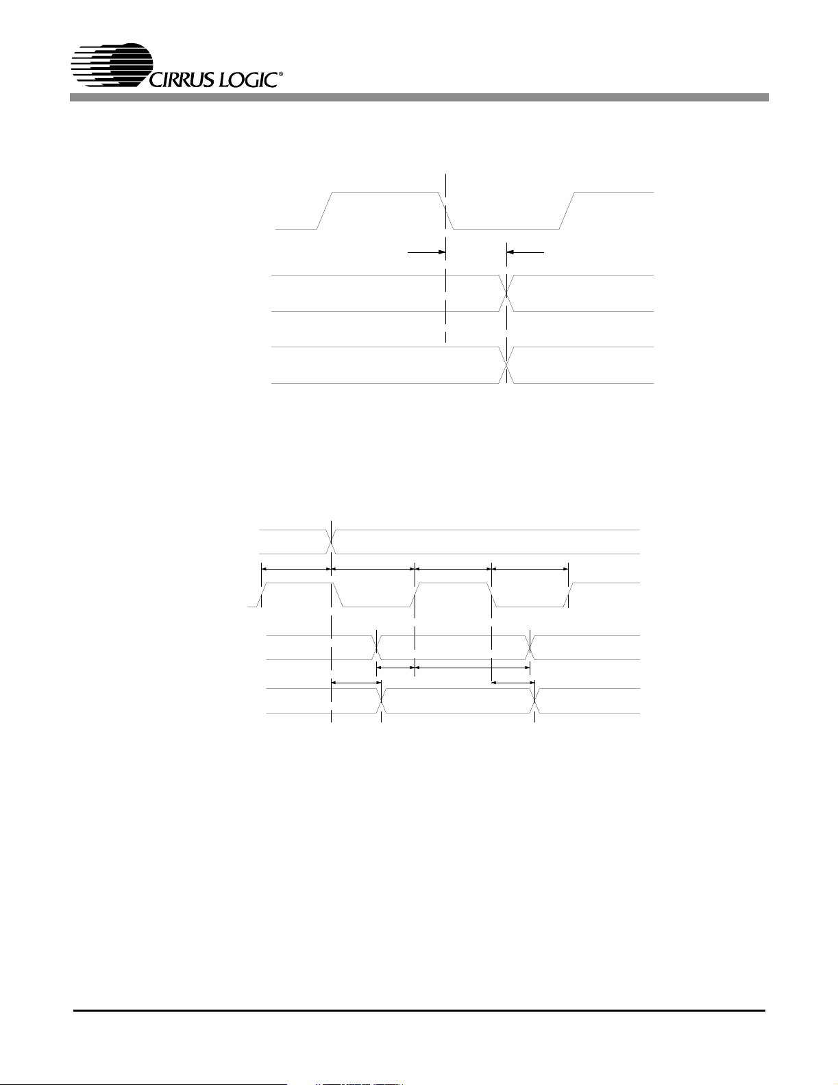
SCLK
(o u tp u t)
LRC K
(o u tp u t)
SDOUT
t
Figure 1. Serial Audio Port Master Mode Timing
CS4228A
mslr
LRCK
(input)
SCLK
(input)
SDIN1
SDIN2
SDIN3
SDOUT
t
lrckd
t
lrp d
t
lrc k s
t
ds
t
sckh
t
dh
MSB
t
sckl
Figure 2. Serial Audio Port Slave Mode Timing
t
dpd
MSB-1
9
CS4228A
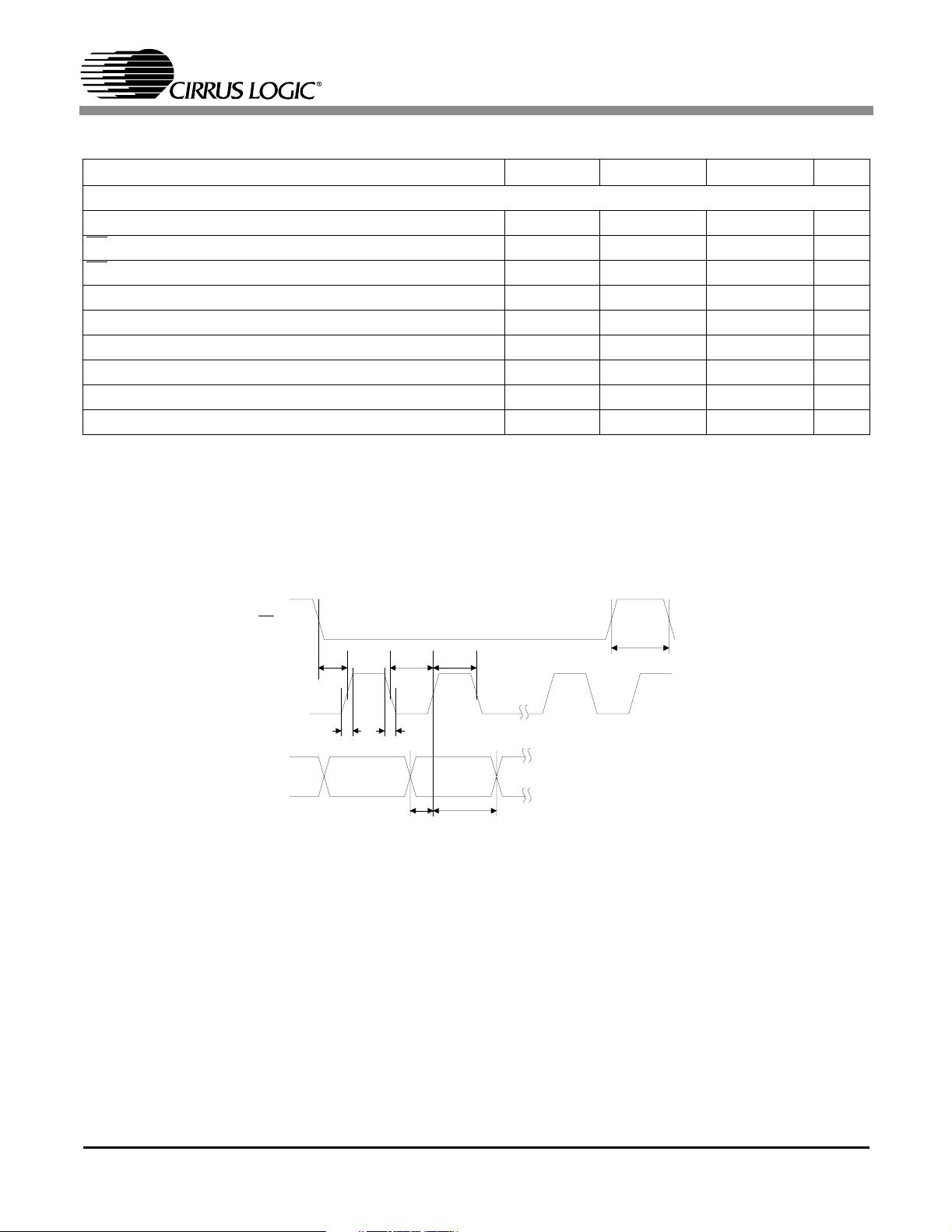
SWITCHING CHARACTERISTICS - CONTROL PORT (Inputs: Logic 0 = 0V, Logic 1 = VL)
Parameter Symbol Min Max Units
SPI Mode (SDOUT > 47 kΩ to GND)
CCLK Clock Frequency f
CS
High Time Between Transmissions t
CS
Falling to CCLK Edge t
CCLK Low Time t
CCLK High Time t
CDIN to CCLK Rising Setup Time t
CCLK Rising to DATA Hold Time (Note 18) t
Rise Time of CCLK and CDIN (Note 19) t
Fall Time of CCLK and CDIN (Note 19) t
sck
csh
css
scl
sch
dsu
dh
r2
f2
Notes: 18. Data must be held for sufficient time to bridge the transition time of CCLK.
19. For F
SCK
<1MHz
-6MHz
1.0 µs
20 ns
66 ns
66 ns
40 ns
15 ns
30 ns
100 ns
CS
CCLK
CDIN
t
t
css
r2
t
scl
t
f2
t
dsu
t
sch
t
dh
Figure 3. SPI Control Port Timing
t
csh
10
CS4228A
SWITCHING CHARACTERISTICS - CONTROL PORT (Inputs: Logic 0 = 0V, Logic 1 = VL)
Parameter Symbol Min Max Units
2
C Mode (SDOUT < 47 kΩ to ground)
I
SCL Clock Frequency f
Bus Free Time Between Transmissions t
Start Condition Hold Time (prior to first clock pulse) t
Clock Low Time t
Clock High Time t
Setup Time for Repeated Start Condition t
SDA Hold Time from SCL Falling (Note 20) t
SDA Setup Time to SCL Rising t
Rise Time of Both SDA and SCL Lines (Note 21) t
Fall Time of Both SDA and SCL Lines t
Setup Time for Stop Condition t
scl
buf
hdst
low
high
sust
hdd
sud
r
f
susp
Notes: 20. Data must be held for sufficient time to bridge the 300 ns transition time of SCL.
21. Pin 11 (SCL/CCLK) of the CS4228A does not have sufficient hysteresis to enable the use of standard
two-wire mode configurations with a resistor pull-up. This issue can be worked around by placing a
Schmitt Trigger buffer, for example a 74VHC14, on the SCL line just prior to the CS4228A. See Figure 5.
This will not affect the operation of the bus in either mode, as pin 6 is an input only.
-100kHz
4.7 µs
4.0 µs
4.7 µs
4.0 µs
4.7 µs
0 µs
250 ns
30 ns
300 ns
4.7 µs
SDA
SCL
Stop S tart
t
buf
SCL
t
hdst
t
low
V+
Figure 5. I
Repeated
Start
t
high
t
hdd
t
sud
t
sust
Figure 4. I2CControlPortTiming
2
CModeSCLBufferExample
t
hdst
t
r
Pin 11
Stop
t
f
t
susp
11

2. TYPICAL CONNECTION DIAGRAM
CS4228A
From Analog Input Stage
+5V
Supply
22
µF
22 µF
Microcontroller
Ferrite B ead
Ω
150
+
100µF
Ω
150
+
+
µ F
100
1
µF
VL
1µF 0.1µF
+
2.2 nf
+
2.2 nf
µ
0.1
2.2 K*
F
0.1µF
0.1µF
+
VL
19
20
17
16
18
12
11
13
14
VA VD
AINL-
AINL+
AINR-
AINR+
FILT
SDA/CDIN
SCL/CCLK
AD0/CS
RST
Ferrite Bead
1
µ
µF0.1
+
F
+5V
Supply
VL
+
9821
VL
FL
23
FR
24
SL
25
Ferrite Bead
µ
1µF0.1
F
ANALOG
FILTER
ANALOG
FILTER
ANALOG
FILTER
+3.0V to + 5V
Supply
Front Left
Front Right
Surround Left
CS4228A
SR
CENTER
SUB
MUTEC
LRCK
SCLK
SDIN1
SDIN2
SDIN3
SDOUT
26
27
28
15
6
5
3
2
1
4
50
ANALOG
FILTER
ANALOG
FILTER
ANALOG
FILTER
VL
Ω
50
Ω
50
Ω
50
Digital Audio
Ω
50
Ω
50
Ω
Peripheral
or
DSP
Surround Right
Center
Subwoofer
12
All unused logic inputs
should be tied to 0V.
AGND DGND
Note: AGND and DGND pins should
both be tied to a comm on ground plane.
MCLK
10722
Figure 6. Recommended Connection Diagram
33 K*
* Required for 2-wire
mode only
External Clock Input
Note : MCLK Logic High is VL

CS4228A
3. FUNCTIONAL DESCRIPTION
3.1 Overview
The CS4228A is a 24-bit audio codec comprised of
2 analog-to-digital converters (ADC) and 6 digitalto-analog converters (DAC), all implemented using single-bit delta-sigma techniques. Other functions integrated with the codec include independent
digital volume controls for each DAC, digital DAC
de-emphasis filters, ADC high-pass filters, an onchip voltage reference, and a flexible serial audio
interface. All functions are configured through a
serial control port operable in SPI mode and in I
2
C
mode. Figure 6 shows the recommended connections for the CS4228A.
3.2 Analog Inputs
3.2.1 Line Level Inputs
AINR+, AINR-, AINL+, and AINL- are the line
level analog inputs (See Figure 6). These pins are
internally biased to a DC operating voltage of approximately 2.3 VDC. AC coupling the inputs preserves this bias and minimizes signal distortion.
Figure 6 shows operation with a single-ended input
source. This source may be supplied to either the
positive or negative input as long as the unused input is connected to ground through capacitors as
shown. When operated with single-ended inputs,
distortion will increase at input levels higher than
-1 dBFS. Figure 7 shows an example of a differential input circuit.
Muting of the stereo ADC is possible through the
ADC Control Byte.
The ADC output data is in 2’s complement binary
format. For inputs above positive full scale or below negative full scale, the ADC will output
7FFFFFH or 800000H, respectively.
3.2.2 High Pass Filter
Digital high pass filters in the signal path after the
ADCs remove any DC offsts present on the analog
inputs. The high pass filter helps prevent audible
“clicks” when switching between audio sources
downstream from the ADCs. The high pass filter
response, given in “High Pass Filter Characteristics”, scales linearly with sample rate. Thus, for
High Rate Mode, the -3 dB frequency at a 96 kHz
sample rate will be equal to 96/44.1 times that at a
sample rate of 44.1 kHz.
signal
VA
10µF
10 k
4.7 k
10 k
+
~8.5k
-
+
10 k
10 k
-
+
+
10
Figure 7. Optional Line Input Buffer
0.1µF
µ
f
150
AIN -
2.2 nf
150
AIN +
13

CS4228A
The high pass filters can be disabled by setting the
HPF bit in the ADC Control register. When asserted, any DC present at the analog inputs will be represented in the ADC outputs. The high pass filter
may also be “frozen” using the HPFZ bit in the
ADC Control register. In this condition, it will remember the DC offset present at the ADC inputs at
the moment the HPFZ bit was asserted, and will
continue to remove this DC level from the ADC
outputs. This is useful in cases where it is desirable
to eliminate a fixed DC offset while still maintaining full frequency response down to DC.
3.3 Analog Outputs
3.3.1 Line Level Outputs
The CS4228A contains on-chip buffer amplifiers
capable of producing line level outputs. These amplifiers are biased to a quiescent DC level of approximately 2.3V. This bias, as well as variations
in offset voltage, are removed using off-chip AC
load coupling.
lution. Volume control changes do not occur instantaneously. Instead they ramp in increments of
0.125 dB at a variable rate controlled by the
RMP1:0 bits in the Digital Volume Control register.
Each output can be independently muted via mute
control bits MUT6-1 in the DAC Mute1 Control
register. When asserted, MUT attenuates the corresponding DAC to its maximum value (90.5 dB).
When MUT is deasserted, the corresponding DAC
MUTEC
AOUT
C=142µF
F
s
10 k
10 k
µ
F
22
+
560
100 k
2SC2878
or
2SC3326
MUN2IIIT1
MUTEDRV
Line Out
C
2.2 k
The delta-sigma conversion process produces high
frequency noise beyond the audio passband, most
of which is removed by the on-chip analog filters.
The remaining out-of-band noise can be attenuated
using an off-chip low pass filter. For most applications, a simple passive filter as shown in Figure 8
can be used. Note that this circuit also serves to
block the DC present at the outputs. Figure 9 gives
an example of a filter which can be used in applications where greater out of band attenuation is desired. The 2-pole Butterworth filter has a -3 dB
frequency of 50 kHz, a passband attenuation of
0.1 dB at 20 kHz, providing optimal out-of-band
filtering for sample rates from 44.1 kHz to 96 kHz.
The filter has and a gain of 1.56, providing a
2 Vrms output signal.
3.3.2 Digital Volume Control
Each DAC’s output level is controlled via the Digital Volume Control register operating over the
range of 0 to 90.5 dB attenuation with 0.5 dB reso-
Figure 8. Passive Output Filter with Mute
1nf
3.57 k
10 µf
3.57 k
+
GND
3.57 k
A
OUT
_
5
7
6
1nf
+
MC33078
2k
100 pf
2-Pole Butterworth Filt er
+
10µf
MUTE
MUTE DRV
Figure 9. Butterworth Output Filter with Mute
Line
Out
2VRMS
14

CS4228A
returns to the attenuation level set in the Digital
Volume Control register. The attenuation is
ramped up and down at the rate specified by the
RMP1:0 bits.
To achieve complete digital attenuation of an incoming signal, Hard Mute controls are provided.
When asserted, Hard Mute will send zero data to a
corresponding pair of DACs. Hard Mute is not
ramped, so it should only be asserted after setting
the two corresponding MUT bits to prevent high
frequency transients from appearing on the DAC
outputs. Hard Mute is controlled by the
HMUTE56/34/12 bits in the DAC Mute2 Control
register.
3.4 Mute Control
The Mute Control pin is typically connected to an
external mute control circuit as shown in Figure 8
and Figure 9. The Mute Control pin is asserted during power up, power down, and when serial port
clock errors are present. The pin can also be controlled by the user via the control port, or automatically asserted when zero data is present on all six
DAC inputs. To prevent large transients on the output, it is desirable to mute the DAC outputs before
the Mute Control pin is asserted. Please see the
MUTEC
more information.
pin in the Pin Descriptions section for
3.5 Clock Generation
The master clock, MCLK, is supplied to the
CS4228A from an external clock source. If MCLK
stops for 10 µs, the CS4228A will enter Power
Down Mode in which the supply current is reduced
as specified under “Power Supply”. In all modes it
is required that the number of MCLK periods per
SCLK and LRCK period be constant.
3.5.1 Clock Source
The CS4228A internal logic requires an external
master clock, MCLK, that operates at multiples of
the sample rate frequency, Fs. The MCLK/Fs ratio
is determined by the CI1:0 bits in the CODEC
Clock Mode register.
3.5.2 Synchronization
The serial port is internally synchronized with
MCLK. If from one LRCK cycle to the next, the
number of MCLK cycles per LRCK cycle changes
by more than 32, the CS4228A will undergo an internal reset of its data paths in an attempt to resynchronize. Consequently, it is advisable to mute the
DACs and clear the DIGPDN bit when changing
from one clock source to another to avoid the output of undesirable audio signals as the device resynchronizes. It is adviseable to ensure that MCLK
complies with the Switching Characteristics at all
times when switching clock sources without resetting the part.
3.6 Digital Interfaces
3.6.1 Serial Audio Interface Signals
The serial audio data is presented in 2's complement binary form with the MSB first in all formats.
The serial interface clock, SCLK, is used for both
transmitting and receiving audio data. SCLK can
be generated by the CS4228A (master mode) or it
can be input from an external source (slave mode).
Mode selection is made with the DMS1:0 bits in
the Serial Port Mode register. The number of
SCLK cycles in one sample period can be set using
the DCK1:0 bits as detailed in the Serial Port Mode
register.
The Left/Right clock (LRCK) is used to indicate
left and right data frames and the start of a new
sample period. It may be an output of the CS4228A
(master mode), or it may be generated by an external source (slave mode). The frequency of LRCK is
the same as the system sample rate, Fs.
SDIN1, SDIN2, and SDIN3 are the data input pins.
SDOUT, the data output pin, carries data from the
two 24-bit ADC's. The serial audio port may also
be operated in One Line Data Mode in which all 6
15

CS4228A
channels of DAC data is input on SDIN1 and the
stereo ADC data is output on SDOUT. Table 1 outlines the serial port input to DAC channel
allocations.
DAC Inputs
SDIN1 left channel
right channel
single line
SDIN2 left channel
right channel
SDIN3 left channel
right channel
Table 1. Serial Audio Port Input Channel Allocations
LRCK
SCLK
SDINx
I2S Mode, Data Valid on Rising Edge of SCLK
Bits/Sample SCLK Rate(s) Notes
16 32, 48, 64, 128 Fs
18 to 24 48, 64, 128 Fs
DAC #1
DAC #2
All 6 DAC channels (BRM)
DAC #3
DAC #4
DAC #5
DAC #6
Left Channel
15 14 13 12 11 10
32, 64 Fs
64 Fs
6543210987
3.6.2 Serial Audio Interface Formats
The digital audio port supports 6 formats, shown in
Figure 10, 11, 12 and 13. These formats are selected using the DDF2:0 bits in the Serial Port Mode
register.
In One Line Data Mode, all 6 DAC channels are input on SDIN1. One Line Data Mode is only available in BRM. See Figure 13 for channel
allocations.
Right Channel
15 14 13 12 11 10
BRM, 48 Fs available in slave mode only
HRM
BRM, 48 Fs available in slave mode only
HRM
6543210987
SDIN1/2/3
SD O U T
16
LRCK
SCLK
Figure 10. I2S Serial Audio Formats
Left C hannel
+3 +2 +1
MSB
-1 -2 -3 -4 -5
Left Justified Mode, Data Valid on Rising Edge of SCLK
Bits/Sample SCLK Rate(s) Notes
16 32, 48, 64, 128 Fs
18 to 24 48, 64, 128 Fs
+5 +4
32, 64 Fs
64 Fs
LSB
BRM, 48 Fs available in slave mode only
HRM
BRM, 48 Fs available in slave mode only
HRM
Figure 11. Left Justified Serial Audio Formats
MSB
-1 -2 -3 -4
Right Channel
+3 +2 +1
+5 +4
LSB

CS4228A
LRCK
SCLK
SDINx
Left Channel
15 14 13 12 11 10
6543210987
Right Justified Mode, Data Valid on Rising Edge of SCLK
Bits/Sample SCLK Rate(s) Notes
16 32, 48, 64, 128 Fs
32, 64 Fs
20 48, 64, 128 Fs
64 Fs
24 48, 64, 128 Fs
64 Fs
BRM, 48 Fs available in slave mode only
HRM
BRM, 48 Fs available in slave mode only
HRM
BRM, 48 Fs available in slave mode only
HRM
Figure 12. Right Justified Serial Audio Formats
64 clks 64 clks
LRCK
SCLK
SDIN1
SDOUT
DAC1 DAC3 DA C5 DAC2 DAC4 DAC6
20 clks
ADCL ADCR
20 clks
Left Channel Right Channel
LSBMSB
LSBMSB LSBMSB LSBMSB LSBMSB LSBMS B MSB
20 clks
20 clks 20 clks 20 clks 20 clks
20 clks
Right Channel
15 14 13 12 11 10
6543210987
One Line Data Mode, Data Valid on Rising Edge of SCLK
Bits/Sample SCLK Rate(s) Notes
20 128 Fs 6 inputs, 2 outputs, BRM only
Figure 13. One Line Data Serial Audio Format
17
CS4228A
3.7 Control Port Signals
Internal registers are accessed through the control
port. The control port may be operated asynchronously with respect to audio sample rate. However,
to avoid potential interference problems, the control port pins should remain static if no register access is required.
The control port has 2 operating modes: SPI mode
2
and I
C mode. In both modes the CS4228A operates as a slave device. Mode selection is determined by the state of the SDOUT pin when RST
transitions from low to high: high for SPI, low for
2
I
C mode. SDOUT is internally pulled high to VL.
A resistive load from SDOUT to GND of less than
47 kΩ will enable I2C mode after a hardware reset.
3.7.1 SPI Mode
In SPI mode, CS is the CS4228A chip select signal,
CCLK is the control port bit clock input, and CDIN
is the input data line. There is no data output line,
therefore all registers are write-only in SPI mode.
Data is clocked in on the rising edge of CCLK.
Figure 13 shows the operation of the control port in
SPI mode. The first 7 bits on CDIN, after CS goes
low, form the chip address (0010000). The eighth
bit is a read/write indicator (R/W), which should always be low to write. The next 8 bits set the Memory Address Pointer (MAP) which is the address of
the register that is to be written. The following
bytes contain the data which will be placed into the
registers designated by the MAP.
The CS4228A has a MAP auto increment capability, enabled by the INCR bit in the MAP register. If
INCR is zero, then the MAP will stay constant for
successive writes. If INCR is 1, then the MAP will
increment after each byte is written, allowing block
reads, or writes, of successive registers.
3.7.2 I2C Mode
In I2C mode, SDA is a bidirectional data line. Data
is clocked into and out of the port by the SCL clock.
The signal timing is shown in Figure 15 and 16. A
Start condition is defined as a falling transition of
SDA while the clock is high. A Stop condition is a
rising transition while the clock is high. All other
transitions of SDA occur while the clock is low.
The first byte sent to the CS4228A after a Start condition consists of a 7 bit chip address field and a
bit (high for a read, low for a write). The AD0
R/W
pin determines the LSB of the chip address field.
The upper 6 bits of the address field must be 00100
and the seventh bit must match AD0. If the operation is to be a write, the second byte is the Memory
Address Ponter (MAP), which selects the register
to be written. The succeeding byte(s) are data. If
the operation is to be a read, the second byte is sent
from the chip to the controller and contains the contents of the register pointed to by the current value
of the MAP.
(input)
CCLK
CDIN
(input)
18
CS
(input)
8 9 10 1145670123 16171819202122
CHIP ADDRESS (WRITE) MAP BYTE
INCR
00100000
MSB
Figure 14. Control Port Timing, SPI Slave Mode Write
R/W
6543210
12 13 14 15
23
DATA DATA +n
76543210
76543210

CS4228A
4567 24 25
INCR 6 54 3210 7 6 10 7 6 10 76 10
ACK
SCL
SDA
0 1 2 3 8 9 12 16 17 18 1910 11 13 14 15 27 28
CHIP ADDRESS (WRITE) MAP BYTE DATA
001000AD00
START
Figure 15. Control Port Timing, I2C Slave Mode Write
168 9 12 13 14 15456701 20 21 2 2 23 24
SCL
SDA
2 3 10 11 17 18 19 25
CHIP ADDRESS (WRITE)
001000AD00
START
MAP BYTE
INCR 6 5 4 3210
ACK
Figure 16. Control Port Timing, I2C Slave Mode Read
Since the read operation can not set the MAP, an
aborted write operation is used as a preamble. As
shown in Figure 16, the write operation is aborted
after the acknowledge for the MAP byte by sending
a stop condition. The following pseudocode illustrates an aborted write operation followed by a read
operation.
Send start condition.
Send 001000x0 chip address & write operation.
Receive acknowledge bit.
Send MAP byte, auto increment off.
Receive acknowledge bit.
Send stop condition, aborting write.
Send start condition.
Send 001000x1 chip address & read operation.
Receive acknowledge bit.
Receive byte, contents of selected register.
Send acknowledge bit.
Send stop condition.
26
ACK
DATA +n
DATA +1
ACKACKACK
DATA + n
STOP
ACK
CHIP ADDRESS (READ)
001000AD01
START
DATA +1
26 27 28
DATA
70 70 70
ACK
Setting the auto increment bit in the MAP allows
successive reads or writes of consecutive registers.
Each byte is separated by an acknowledge bit.
3.8 Control Port Bit Definitions
All registers are read/write, except the Chip Status
register which is read-only. For more detailed information, see the bit definition tables.
3.9 Power-up/Reset/Power Down Mode
Upon power up, the user should hold RST = 0 until
the power supplies and clocks stabilize. In this
state, the control registers are reset to their default
settings, and the device remains in a low power
mode in which the control port is inactive. The part
may be held in a low power reset state by clearing
the DIGPDN bit in the Chip Control register. In this
state, the digital portions of the CODEC are in reset, but the control port is active and the desired
register settings can be loaded. Normal operation is
achieved by setting the DIGPDN bitto1,atwhich
time the CODEC powers up and normal operation
begins.
STOP
NO
ACK
STOP
19

CS4228A
The CS4228A will enter a stand-by mode if the
master clock source stops for approximately 10 µs
or if the number of MCLK cycles per LRCK period
varies by more than 32. Should this occur, the control registers retain their settings.
The CS4228A will mute the analog outputs, assert
the MUTEC pin and enter the Power Down Mode
if the supply drops below approximately 4V.
3.10 Power Supply, Layout, and
Grounding
The CS4228A requires careful attention to power
supply and grounding details. VA is normally supplied from the system 5 VDC analog supply. VD is
from a 5 VDC digital supply. VL should be from
the supply used for the devices digitally interfacing
with the CS4228A. Attention should be placed on
the VL and VD power up sequence such that the
VD supply is applied at the same time or after VL
supply is applied (see “Specified Operating Conditions” on page 4).
AGND and DGND pins should both be tied to a
solid ground plane surrounding the CS4228A. The
system analog and digital ground planes should not
be separated under normal circumstances. A solid
ground plane underneath the part is recommended.
Decoupling capacitors should be mounted and
routed in such a way as to minimize the circuit path
length from the CS4228A supply pin or FILT pin,
through the capacitor, and back to the applicable
CS4228A AGND or DGND pin. The small value
ceramic capacitors should be closest to the part. In
some cases, ferrite beads in the VL, VD and VA
supply lines, and low-value resistances (~ 50 Ω) in
series with the LRCK, SCLK, SDIN and SDOUT
lines can help reduce coupling of digital signals
into the analog portions of the CS4228A.
Both capacitors on the FILT pin should be as close
to the CS4228A as possible. Any noise that couples
onto the FILT pin will couple directly onto all of
the analog outputs. Please see the CDB4228 evaluation board data sheet for recommended layout of
the decoupling components.
20

CS4228A
4. REGISTER QUICK REFERENCE
Addr Function 7 6 5 4 3 2 1 0
MAP Memory Address
Pointer
0x01 CODEC Clock Mode HRM Reserved
default=0x04
INCR Reserved Reserved MAP4 MAP3 MAP2 MAP1 MAP0
1000 0 0 0 1
Reserved
00
0
Reserved CI1 CI0 Reserved Reserved
00 1 00
0x02 Chip Control DIGPDN Reserved Reserved ADCPDN
default=0x80
0x03 ADC Control MUTL MUTR HPF HPFZ Reserved Reserved Reserved Reserved
default=0x00
0x04 DAC Mute1 Control MUT6 MUT5 MUT4 MUT3 MUT2 MUT1 RMP1 RMP0
default=0xFC
0x05 DAC Mute2 Control MUTEC MUTCZ Reserved Reserved HMUTE56 HMUTE34 HMUTE12 Reserved
default=0x80
0x06 DAC De-emphasis
Control
default=0x80 1 0 0 0 0 0 0 0
0x07 DAC 1 Volume Cntrl Vol7 Vol6 Vol5 Vol4 Vol3 Vol2 Vol1 Vol0
default=0x00
0x08 DAC 2 Volume Cntrl Vol7 Vol6 Vol5 Vol4 Vol3 Vol2 Vol1 Vol0
default=0x00
0x09 DAC 3 Volume Cntrl Vol7 Vol6 Vol5 Vol4 Vol3 Vol2 Vol1 Vol0
default=0x00
0x0A DAC 4 Volume Cntrl Vol7 Vol6 Vol5 Vol4 Vol3 Vol2 Vol1 Vol0
default=0x00
0x0B DAC 5 Volume Cntrl Vol7 Vol6 Vol5 Vol4 Vol3 Vol2 Vol1 Vol0
default=0x00
0x0C DAC 6 Volume Cntrl Vol7 Vol6 Vol5 Vol4 Vol3 Vol2 Vol1 Vol0
default=0x00
0x0D
Serial Port Mode
default=0x84
0x0E
Chip Status
read only
1000 0 0 0 0
0000 0 0 0 0
1111 1 1 0 0
1000 0 0 0 0
DEMS1 DEMS0 DEM6 DEM5 DEM4 DEM3 DEM2 DEM1
0000 0 0 0 0
0000 0 0 0 0
0000 0 0 0 0
0000 0 0 0 0
0000 0 0 0 0
0000 0 0 0 0
DCK1 DCK0 DMS1 DMS0 Reserved DDF2 DDF1 DDF0
1000 0 1 0 0
CLKERR ADCOVL Reserved Reserved Reserved Reserved Reserved Reserved
XX0 0 0 0 0 0
DACPDN56 DACPDN34 DACPDN12
Reserved
7654 3 2 1 0
Table 2. User Registers
21

CS4228A
5. REGISTER DESCRIPTIONS
All registers are read/write except for Chip Status, which is read only. See the following bit definition tables
for bit assignment information. The default state of each bit after a power-up sequence or reset is listed
in the tables underneath each bit’s label. Default values are also marked in the text with an asterisk.
5.1 Memory Address Pointer (MAP)
Not a register
76543210
INCR RESERVED MAP4 MAP3 MAP2 MAP1 MAP0
10000001
INCR memory address pointer auto increment control
0 - MAP is not incremented automatically.
*1 - internal MAP is automatically incremented after each read or write.
MAP4:0 Memory address pointer (MAP). Sets the register address that will be read or written by the con-
trol port.
5.2 CODEC Clock Mode
Address 0x01
76543210
HRM RESERVED CI1 CI0 RESERVED
00000100
HRM Sets the sample rate mode for the ADCs and DACs
*0- BaseRateMode(BRM)supportssampleratesupto50kHz
1 - High Rate Mode (HRM) supports sample rates up to 100 kHz. Typically used for
96 kHz sample rate.
CI1:0 Specifies the ratio of MCLK to the sample rate of the ADCs and DACs (Fs)
CI1:0 BRM (Fs) HRM (Fs)
0 128 64
*1 256 128
2384192
3512256
5.3 Chip Control
Address 0x02
7 6543210
DIGPDN
1 0000000
RESERVED ADCPDN DACPDN56 DACPDN34 DACPDN12 RESERVED
DIGPDN
ADCPDN Power down the analog section of the ADC
22
Power down the digital portions of the CODEC
0 - Digital power down.
*1 - Normal operation
*0 - Normal
1 - ADC power down.

CS4228A
DACPDN12 Power down the analog section of DAC 1 and 2
*0 - Normal
1 - Power down DAC 1 and 2.
DACPDN34 Power down the analog section of DAC 3 and 4
*0 - Normal
1 - Power down DAC 3 and 4.
DACPDN56 Power down the analog section of DAC 5 and 6
*0 - Normal
1 - Power down DAC 5 and 6.
5.4 ADC Control
Address 0x03
76543210
MUTL MUTR HPF HPFZ RESERVED
00000000
MUTL, MUTR ADC left and right channel mute control
*0 - Normal
1 - Selected ADC output muted
HPF ADC DC offset removal. See “High Pass Filter” for more information
*0 - Enabled
1 - Disabled
HPFZ ADC DC offset averaging freeze. See “High Pass Filter” for more information
*0 - Normal. The DC offset average is dynamically calculated and subtracted from in-
coming
ADC data.
1 - Freeze. The DC offset average is frozen at the current value and subtracted from
incoming ADC data. Allows passthru of DC information.
5.5 DAC Mute1 Control
Address 0x04
76543210
MUT6 MUT5 MUT4 MUT3 MUT2 MUT1 RMP1 RMP0
11111100
MUT6 - MUT1 Mute control for DAC6 - DAC1 respectively. When asserted, the corresponding DAC is digitally
attenuated to its maximum value (90.5 dB). When deasserted, the corresponding DAC attenuation value returns to the value stored in the corresponding Digital Volume Control register. The
attenuation value is ramped up and down at the rate specified by RMP1:0.
0 - Normal output level
*1 - Selected DAC output fully attenuated.
RMP1:0 Attenuation ramp rate.
*0 - 0.5 dB change per 4 LRCKs
1- 0.5dBchangeper8LRCKs
2 - 0.5 dB change per 16 LRCKs
3 - 0.5 dB change per 32 LRCKs
23

CS4228A
5.6 DAC Mute2 Control
Address 0x05
76543210
MUTEC MUTCZ RESERVED HMUTE56 HMUTE34 HMUTE12 RESERVED
10000000
MUTEC Controls the MUTEC
0 - Normal operation
*1 - MUTEC
MUTCZ Automatically asserts the MUTEC
zerosonallsixDACinputswillcausetheMUTEC
value on any DAC input will cause the MUTEC
*0 - Disabled
1 - Enabled
HMUTE56/34/12 Hard mute the corresponding DAC pair. When asserted, zero data is sent to the corresponding
DAC pair causing an instantaneous mute. To prevent high frequency transients on the outputs,
a DAC pair should be fully attenuated by asserting the corresponding MUT6-MUT1 bits in the
DAC Mute Control register or by writing 0xFF to the corresponding Digital Volume Control registers before asserting HMUTE.
*0 - Normal operation
1 - DAC pair is muted
pin
pin asserted low
pin on consecutive zeros. When enabled, 512 consecutive
pin to be asserted low. A single non-zero
pin to deassert.
5.7 DAC De-emphasis Control
Address 0x06
76543210
DEMS1 DEMS0 DEM6 DEM5 DEM4 DEM3 DEM2 DEM1
10000000
DEMS1:0 Selects the DAC de-emphasis response curve.
0- Reserved
1 - De-emphasis for 48 kHz
*2 - De-emphasis for 44.1 kHz
3 - De-emphasis for 32 kHz
DEM6 - DEM1 De-emphasis control for DAC6 - DAC1 respectively
*0 - De-emphasis off
1 - De-emphasis on
5.8 Digital Volume Control
Addresses 0x07, 0x08, 0x09, 0x0A, 0x0B, 0x0C
76543210
VOLn
00000000
VOL6 - VOL1 Address 0x0C - 0x07 sets the attenuation level for DAC 6 - DAC1 respectively. The attenutation
level is ramped up and down at the rate specified by RMP1:0 in the DAC Volume Control Setup
register.
0 - 181 represents 0 to 90.5 dB of attenuation in 0.5 dB steps.
24

CS4228A
5.9 Serial Port Mode
Address 0x0D
76543210
DCK1 DCK0 DMS1 DMS0 RESERVED DDF2 DDF1 DFF0
10000100
DCK1:0 Sets the number of Serial Clocks (SCLK) per Fs period (LRCLK)
DCK1:0 BRM (Fs) HRM (Fs)
032(1)(3)
148(2)(3)
2 *64 32 (1)
3 128 64
Notes: 1. All formats will default to 16 bits
2. Slave mode only
3. Invalid mode
DMS1:0 Sets the master/slave mode of the serial audio port
*0 - Slave (External LRCLK, SCLK)
1- Reserved
2- Reserved
3- Master(No48FsSCLKinBRM)
DDF2:0 Serial Port Data Format
0 - Right Justified, 24-bit
1 - Right Justified, 20-bit
2 - Right Justified, 16-bit
3 - Left Justified, maximum 24-bit
*4 - I
5 - One-line Data Mode, available in BRM only
6- Reserved
7- Reserved
2
S compatible, maximum 24-bit
5.10 Chip Status
Address 0x0E
7 6543210
CLKERR ADCOVL RESERVED
XX000000
CLKERR Clocking system status, read only
0- NoError
1 - No MCLK is present, or a request for clock change is in progress
ADCOVL ADC overflow bit, read only
0 - No overflow
1- ADCoverflowhasoccurred
25

6. PIN DESCRIPTION
t
CS4228A
Serial Audio Data In 3 SDIN3 SUB Analog Out #6,Subwoofer
Serial Audio Data In 2 SDIN2 CENTER Analog Out #5, Center
Serial Audio Data In 1 SDIN1 SR Analog Out #4, Surround Righ
Serial Audio Data Out SDOUT SL Analog Out #3, Surround Left
Serial Clock SCLK FR Analog Out #2, Front Right
Left/Right Clock LRCK FL Analog Out #1, Front Left
Digital Ground DGND AGND Analog Ground
Digital Power VD VA Analog Power
Digital Interface Power VL AINL+ Left Channel Analog Input+
Master Clock MCLK AINL- Left Channel Analog Input-
SCL/CCLK SCL/CCLK FILT Internal Voltage Filter
SDA/CDIN SDA/CDIN AINR- Right Channel Analog Input-
AD0/CS
Reset RST
SDIN1, SDIN2,
SDIN3
SDOUT 4 Serial Audio Data Out (Output) - Two's complement MSB-first serial data is output on this
SCLK 5 Serial Clock (Bidirectional) - Clocks serial data into the SDIN1, SDIN2, and SDIN3 pins,
1, 2, 3 Serial Audio Data In (Input) - Two's complement MSB-first serial audio data is input on this
AD0/CS AINR+ Right Channel Analog Input+
pin. The data is clocked into SDIN1, SDIN2, SDIN3 via the serial clock and the channel is
determined by the Left/Right clock. The required relationship between the Left/Right clock,
serial clock and serial data is defined by the Serial Mode Register. The options are detailed
in Figures 10, 11, 12, and 13.
pin. The data is clocked out of SDOUT via the serial clock and the channel is determined by
the Left/Right clock. The required relationship between the Left/Right clock, serial clock and
serial data is defined by the Serial Mode Register. The options are detailed in Figures 10,
11, 12 and 13.
The state of the SDOUT pin during reset is used to set the Control Port Mode (I
When RST
state of the pin. A weak internal pull up is present such that a resistive load less than 47 kΩ
will pull the pin low, and the control port mode is I
greater than 47 kΩ during reset, the control port mode is SPI.
and out of the SDOUT pin. The pin is an output in master mode, and an input in slave
mode.
In master mode, SCLK is configured as an output. MCLK is divided internally to generate
SCLK at the desired multiple of the sample rate.
In slave mode, SCLK is configured as an input. The serial clock can be provided externally,
or the pin can be grounded and the serial clock derived internally from MCLK.
The required relationship between the Left/Right clock, serial clock and serial audio data is
defined by the Serial Port Mode register. The options are detailed in Figures 10, 11, 12
and 13.
is low, SDOUT is configured as an input, and the rising edge of RST latches the
1
1
2
2
3
4
5
5
6
6
7
8
9
10
11
12
13
28
27
26
25
24
23
22
21
20
19
18
17
16
1514
MUTEC Mute Control
2
C. When the resistive load on SDOUT is
2
C or SPI).
26

CS4228A
LRCK 6 Left/Right Clock (Bidirectional) - The Left/Right clock determines which channel is cur-
rently being input or output on the serial audio data output, SDOUT. In Master mode, LRCK
is an output, in Slave Mode, LRCK is an input whose frequency must be equal to Fs and
synchronous to the Master clock.
Audio samples in Left/Right pairs represent simultaneously sampled analog inputs whereas
Right/Left pairs will exhibit a one sample period difference. The required relationship
between the Left/Right clock, serial clock and serial data is defined by the Serial Port Mode
register. The options are detailed in Figures 10, 11, 12 and 13
DGND 7 Digital Ground (Input) - Digital Ground Reference.
VD 8 Digital Power (Input) - Digital Power Supply.
VL 9 Digital Interface Power (Input) - Digital interface power supply. All digital output voltages
and input threshholds scale with VL.
MCLK 10 Master Clock (Input) - The master clock frequency must be either 128x, 256x, 384x or
512x the input sample rate in Base Rate Mode (BRM) and either 64x, 128x, 192x, or 256x
the input sample rate in High Rate Mode (HRM). Table 3 illustrates several standard audio
sample rates and the required master clock frequencies. The MCLK/Fs ratio is set by the
CI1:0 bits in the CODEC Clock Mode register.
Sample
Rate
(kHz)
32 - - - - 4.0960 8.1920 12.2880 16.3840
44.1 - - - - 5.6448 11.2896 16.9344 22.5792
48 - - - - 6.1440 12.2880 18.4320 24.5760
64 4.0960 8.1920 12.2880 16.3840 - - - -
88.2 5.6448 11.2896 16.9344 22.5792 - - - 96 6.1440 12.2880 18.4320 24.5760 - - - -
64x 128x 192x 256x 128x 256x 384x 512x
HRM BRM
MCLK (MHz)
Table 3. Common Master Clock Frequencies
SCL/CCLK 11 Serial Control Interface Clock (Input) - Clocks the serial control data into or out of
SDA/CDIN.
SDA/CDIN 12 Serial Control Data I/O (Bidirectional/Input)-InI
port data line. A pull up resistor must be provided for proper open drain output operation. In
SPI mode, CDIN is the control port data input line. The state of the SDOUT pin during reset
is used to set the control port mode.
ADO/CS
RST
MUTEC 15 Mute Control (Output) - The Mute Control pin goes low during the following conditions:
13 AddressBit0/ChipSelect(Input) - In I2C mode, AD0 is the LSB of the chip address. In
SPI mode, CS
14 Reset (Input) - When low, the device enters a low power mode and all internal registers
are reset to the default settings, including the control port. The control port can not be
accessed when reset is low.
When high, the control port and the CODEC become operational.
power-up initialization, power-down, reset, no master clock present, or if the master clock to
left/right clock frequency ratio is incorrect. The Mute Control pin can also be user controlled
by the MUTEC bit in the DAC Mute2 Control register. Mute Control can be automatically asserted when 512 consecutive zeros are detected on all six DAC inputs, and automatically
deasserted when a single non-zero value is sent to any of the six DACs. The mute on zero
function is control
is intended to be used as a control for an external mute circuit to achieve a very low noise
floor during periods when no audio is present on the DAC outputs, and to prevent the clicks
and pops that can occur in any single supply system. Use of the Mute Control pin is not man-
tory but recommended.
da
is used as a enable for the control port interface.
led by the MUTCZ bit in the DAC Mute2 Control register. The MUTEC pin
2
C mode, SDA is a bidirectional control
27

CS4228A
AINR+, AINR-,
AINL+, AINL-
FILT 18 Internal Voltage Filter (Output) - Filter for internal circuits. An external capacitor is required
VA 21 Analog Power (Input) - Power for the analog and reference circuits.
AGND 22 Analog Ground (Input) - Analog ground reference.
FR,FL,SR,SL
SUB, CENTER
16, 17, 19, 20 Differential Analog Inputs (Input) - The analog signal inputs are presented differentially to
the modulators via the AINR+/- and AINL+/- pins. The + and - input signals are 180° out of
phase resulting in a nominal differential input voltage of twice the input pin voltage. These
pins are biased to the internal reference voltage. A passive anti-aliasing filter is required for
best performance, as shown in Figure 6. The inputs can be driven at -1 dB FS single-ended
if the unused input is connected to ground through a large value capacitor. A single ended
to differential converter circuit can also be used for slightly better performance.
from FILT to analog ground, as shown in Figure 6. FILT is not intended to supply external
current. FILT+ has a typical source impedance of 250 kΩ and any current drawn from this
pin will alter device performance. Care should be taken during board layout to keep dynamic
signal traces away from this pin.
23, 24, 25,
26, 27, 28
Analog Outputs (Output) - Analog outputs from the DACs. The full scale analog output level
is specified in the Analog Characteristics specifications table. The amplitude of the outputs
is controlled by the Digital Volume Control registers 0x07 - 0x0C.
28

7. PARAMETER DEFINITIONS
Dynamic Range
The ratio of the full scale RMS value of the signal to the RMS sum of all other spectral
components over the specified bandwidth. Dynamic range is a signal-to-noise measurement
over the specified bandwidth made with a -60 dBFS signal. 60 dB is then added to the resulting
measurement to refer the measurement to full scale. This technique ensures that the distortion
components are below the noise level and do not effect the measurement. This measurement
technique has been accepted by the Audio Engineering Society, AES17-1991, and the
Electronic Industries Association of Japan, EIAJ CP-307.
Total Harmonic Distortion + Noise
The ratio of the RMS value of the signal to the RMS sum of all other spectral components over
the specified bandwidth (typically 20 Hz to 20 kHz), including distortion components.
Expressed in decibels. ADCs are measured at -1 dBFs as suggested in AES 17-1991 Annex A.
Idle Channel Noise / Signal-to-Noise-Ratio
The ratio of the RMS analog output level with 1 kHz full scale digital input to the RMS analog
output level with all zeros into the digital input. Measured A-weighted over a 10 Hz to 20 kHz
bandwidth. Units in decibels. This specification has been standardized by the Audio
Engineering Society, AES17-1991, and referred to as Idle Channel Noise. This specification has
also been standardized by the Electronic Industries Association of Japan, EIAJ CP-307, and
referred to as Signal-to-Noise-Ratio.
CS4228A
Total Harmonic Distortion (THD)
THD is the ratio of the test signal amplitude to the RMS sum of all the in-band harmonics of
the test signal. Units in decibels.
Interchannel Isolation
A measure of crosstalk between channels. Measured for each channel at the converter's output
with no signal to the input under test and a full-scale signal applied to the other channel. Units
in decibels.
Frequency Response
A measure of the amplitude response variation from 20 Hz to 20 kHz relative to the amplitude
response at 1 kHz. Units in decibels.
Interchannel Gain Mismatch
For the ADCs, the difference in input voltage that generates the full scale code for each
channel. For the DACs, the difference in output voltages for each channel with a full scale
digital input. Units are in decibels.
29

Gain Error
The deviation from the nominal full scale output for a full scale input.
Gain Drift
The change in gain value with temperature. Units in ppm/°C.
Offset Error
For the ADCs, the deviation in LSBs of the output from mid-scale with the selected input
grounded. For the DACs, the deviation of the output from zero (relative to CMOUT) with midscale input code. Units are in Volts.
CS4228A
30

8. PACKAGE DIMENSIONS
28L SSOP PACKAGE DRAWING
N
CS4228A
D
E
A2
A
E1
1
∝
2
b
SIDE VIEW
1
23
e
TOP VIEW
INCHES MILLIMETERS NOTE
DIM MIN NOM MAX MIN NOM MAX
A -- -- 0.084 -- -- 2.13
A1 0.002 0.006 0.010 0.05 0.15 0.25
A2 0.064 0.069 0.074 1.62 1.75 1.88
b 0.009 -- 0.015 0.22 -- 0.38 2, 3
D 0.390 0.4015 0.413 9.90 10.20 10.50 1
E 0.291 0.307 0.323 7.40 7.80 8.20
E1 0.197 0.209 0.220 5.00 5.30 5.60 1
e 0.022 0.026 0.030 0.55 0.65 0.75
L 0.025 0.0354 0.041 0.63 0.90 1.03
∝
0° 4° 8° 0° 4° 8°
A1
SEATING
PLANE
L
END VIEW
JEDEC #: MO-150
Controlling Dimension is Millimeters
Notes: 1.“D” and “E1” are reference datums and do not included mold flash or protrusions, but do include mold
mismatch and are measured at the parting line, mold flash or protrusions shall not exceed 0.20 mm per
side.
2.Dimension “b” does not include dambar protrusion/intrusion. Allowable dambar protrusion shall be
0.13 mm total in excess of “b” dimension at maximum material condition. Dambar intrusion shall not
reduce dimension “b” by more than 0.07 mm at least material condition.
3.These dimensions apply to the flat section of the lead between 0.10 and 0.25 mm from lead tips.
31

 Loading...