

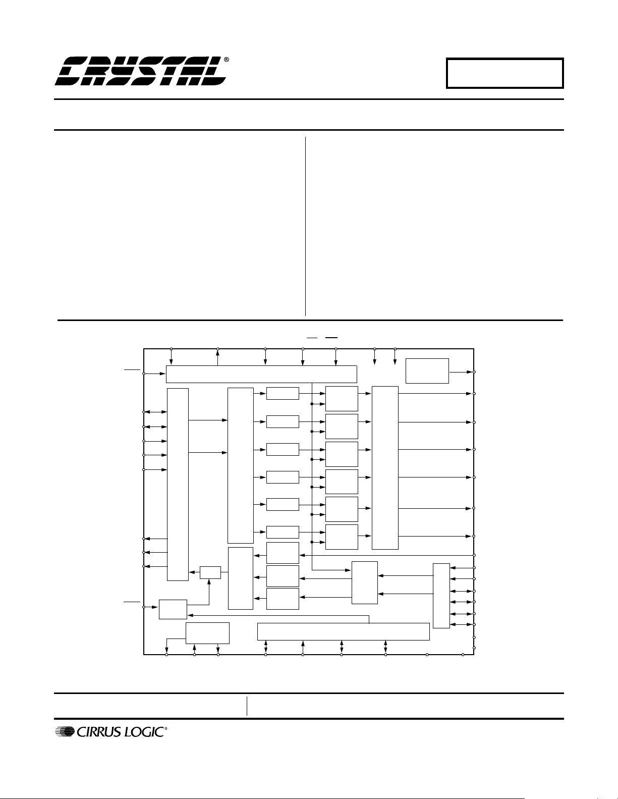
Six Channel, 20-Bit Codec
CS4227
Features
l Stereo 20-bit A/D Converters
l Six 20-bit D/A Converters
l 108 dB DAC Signal-to-Noise Ratio (EIAJ)
l Mono 20-bit A/D Converter
l Programmable Input Gain & Output
Attenuation
l On-chip Anti-aliasing and Output Smoothing
Filters
l De-emphasis for 32 kHz, 44.1 kHz, 48 kHz
I
PDN
LRCK
SCLK
SDIN1
SDIN2
SDIN3
SDOUT1
SDOUT2
OVL
DEM
SCL/CCLK
DEM
CLKOUT XTI XTO
Serial Audio Data Interface
Clock Osc/
SDA/CDOUT
Control Port
MUX
Divider
AD1/CDIN AD0/CS SPI/I2C
DAC#1
DAC#2
DAC#3
DAC#4
Digital Filters
DAC#5
DAC#6
Mono
ADC
Left
ADC
Digital Filters
HOLD
Right
ADC
DATAUX
Description
The CS4227 is a si ng le- c hi p codec providing st ereo analog-to-digital and six digital-to-anal og converters us ing
delta-sigma conversion techniques. This +5 V device
also contains volume controls that are independently selectable for each of the six D/A chan nels. Applications
include Dolby
3™ home theater syste ms, DSP based car audio sy stems, and other multi-channel applications.
ORDERING INFORMATION
CS4227-KQ -10° to +70° C 44-pin TQFP
CS4227-BQ -40° to +85° C 44-pin TQFP
CDB4227 Evaluation Board
Volume
Control
Volume
Control
Volume
Control
Volume
Control
Volume
Control
Volume
Control
Auxiliary Input
LRCKAUX SCLKAUX DGND1 DGND2
®
Pro-logic™, THX®, and Dolby Digital AC-
VD+
VA+
Input
Voltage
Reference
Output Stage
Analog Low Pass and
Gain
Input MUX
CMOUT
AOUT1
AOUT2
AOUT3
AOUT4
AOUT5
AOUT6
AINAUX
AIN1L
AIN1R
AIN2L
AIN2R
AIN3L
AIN3R
AGND1
AGND2
Preliminary Product Information
P.O. Box 17847, Austin, Texas 78760
(512) 445 7222 FAX: (512) 445 7581
http://www.cirrus.com
This document contains information for a new product.
Cirrus Logic reserves the right to modify this product without notice.
Copyright Cirrus Logic, Inc. 1999
(All Rights Reserved)
DS281PP2
SEP ‘99
1

TABLE OF CONTENTS
1. CHARACTERISTICS AND SPECIFICATIONS .................................. ....... ...... ....... ...... ....... ..... 4
ANALOG CHARACTERISTICS................................................................................................ 4
SWITCHING CHARACTERISTICS ....... ....... ...... ....... ...... ...... ....... ...... ....... ...... ....... ...... ....... ..... 6
SWITCHING CHARACTERISTICS - CONTROL PORT........................................................... 8
ABSOLUTE MAXIMUM RATINGS .........................................................................................10
RECOMMENDED OPERATING CONDITIONS.....................................................................10
DIGITAL CHARACTERISTICS...............................................................................................10
2. FUNCTIONAL DESCRIPTION ...............................................................................................12
2.1 Overview ..........................................................................................................................12
2.2 Analog Inputs ................................................................................................................... 12
2.2.1 Line Level Inputs .................................................................................................12
2.2.2 Adjustable Input Gain ..........................................................................................13
2.2.3 High Pass Filter ...................................................................................................13
2.3 Analog Outputs ................................................................................................................ 13
2.3.1 Line Level Outputs .............................................................................................. 13
2.3.2 Output Level Attenuator ...................................................................................... 14
2.4 Clock Generation ............................................................................................................. 14
2.4.1 Clock Source .......................................................................................................14
2.4.2 Master Clock Output ...........................................................................................14
2.4.3 Synchronization ................................................................................................... 14
2.5 Digital Interfaces .............................................................................................................. 15
2.5.1 Audio DSP Serial Interface Signals ..................................................................... 15
2.5.2 Audio DSP Serial Interface Formats ...................................................................15
2.5.3 Auxiliary Audio Port Signals ................................................................................15
2.5.4 Auxiliary Audio Port Formats ...............................................................................15
2.6 Control Port Signals .........................................................................................................17
2.6.1 SPI Mode ............................................................................................................17
2C®
2.6.2 I
2.6.3 Control Port Bit Definitions ..................................................................................18
2.7 Power-up/Reset/Power Down Mode ................................................................................18
2.8 DAC Calibration ...............................................................................................................19
2.9 De-Emphasis ...................................................................................................................19
2.10 Hold Function .................................................................................................................19
Mode ...........................................................................................................18
CS4227
Contacting Cirrus Logic Support
For a complete listing of Direct Sales, Distributor, and Sales Representative contacts, visit the Cirrus Logic web site at:
http://www.cirrus.com/corporate/contacts/
Dolby is a registered trademark of Dolby Labratories Licensing Corporation.
Pro Logic, and AC-3 are trademarks of Dolby Labratories Licensing Corporation.
THX is a registered trademark of LucasArts Entertainment Company.
Preliminary product info rmation describes products which are i n p r od ucti on, b ut for which full characteriza ti on da t a i s not yet available. Advance produ ct i nf or -
mation describes products which are in development and subject to development changes. Cirrus Logic, Inc. has made best efforts to ensure that the information
contained in this document is accurate and reli able. However , the i nformati on is sub ject to change with out no tice and i s provi ded “AS IS” withou t warranty of
any kind (express or implied). No responsibility is assumed by Cirrus Logic, Inc. for the use of this information, nor for infringements of patents or other rights
of third parties. This document i s the propert y of Cirru s Logic, Inc. and implie s no licen se under patent s, copyri ghts, trademarks, or tr ade secrets. No part of
this publication may be copied, reproduced , stored in a retrieval system, or transmitted, in any form or by any means (electronic, mechanical, photographic, or
otherwise) without the pri or wri tt en consen t of Ci rrus Logic, Inc. Items from any Cirrus Logic websi t e or di sk may be pri nted for use by the user. However, no
part of the printout or electronic files may be copied, reproduced, stored in a retrieval system, or transmitted, in any form or by any means (electronic, mechanical,
photographic, or otherwise) without the prior written consent of Cirrus Logic, Inc.Furthermore, no part of this publication may be used as a basis for manufacture
or sale of any items without the prior written consent of Cirrus Logic, Inc. The names of products of Cirrus Logic, Inc. or other vendors and suppliers appearing
in this document may be trademarks or service marks of their respective owners which may be registered in some jurisdictions. A list of Cirrus Logic, Inc. trademarks and service marks can be found at http://www.cirrus.com.
2 DS281PP2

2.11 Power Supply, Layout, and Grounding .......................................................................... 19
2.12 ADC and DAC Filter Response Plots ............................................................................ 20
3. PIN DESCRIPTIONS ....................... ...... ....... ............................................. ...... ....... ................ 29
4. PARAMETER DEFINITIONS .................................................................................................. 33
5. PACKAGE DIMENSIONS ...................................................................................................... 34
LIST OF FIGURES
Figure 1. Audio Ports Master Mode Timing..................................................................................... 7
Figure 2. Audio Ports Slave Mode and Data I/O Timing................................................................. 7
Figure 3. Control Port SPI Mode..................................................................................................... 8
Figure 4. Control Port I
Figure 5. Recommended Connection Diagram............................................................................. 11
Figure 6. Optional Line Intput Buffer............................................................................................. 12
Figure 7. Butterworth Filters................... ...... ....... ...... ............................................. ....................... 13
Figure 8. Audio DSP and Auxiliary Port Data Input Formats ........................................................ 16
Figure 9. Audio DSP Port Data Output Formats ........................................................................... 16
Figure 10. One Data Line Modes..................................................................................................16
Figure 11. Control Port Timing, SPI Mode .................................................................................... 17
Figure 12. Control Port Timing, I
Figure 13. De-emphasis Curve..................................................................................................... 19
Figure 14. Suggested Layout Guideline........................................................................................ 20
Figure 15. 20-bit ADC Filter Response......................................................................................... 21
Figure 16. 20-bit ADC Passband Ripple....................................................................................... 21
Figure 17. 20-bit ADC Transition Band......................................................................................... 21
Figure 18. DAC Frequency Response.......................................................................................... 21
Figure 19. DAC Passband Ripple................................................................................................. 21
Figure 20. DAC Transition Band................................................................................................... 21
CS4227
2
C Mode.......................... ...... ....... ...... ...... ....... ...... ....... ...... ......................... 9
2C®
Mode................................................................................... 18
LIST OF TABLES
Table 1. Single-ended vs Differential Input Pin Assignments.............................................................. 12
Table 2. High Pass Filter Characteristics ............................................................................................ 13
Table 3. DSP Serial Input Ports........................................................................................................... 15
DS281PP2 3
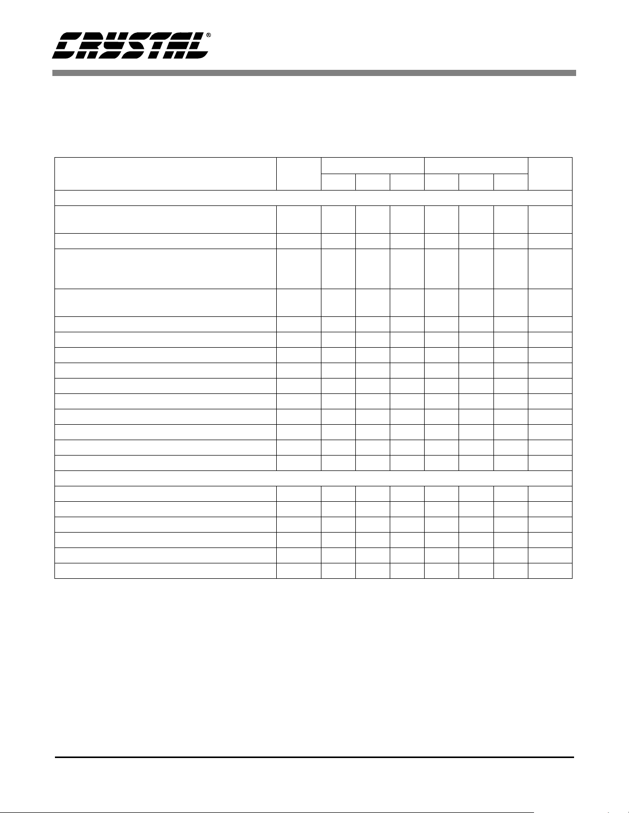
1. CHARACTERISTICS AND SPECIFICATIONS
CS4227
ANALOG CHARACTERISTICS (T
Fs = 44.1 kHz; Measurement Bandwidth is 20 Hz to 20 kHz; Local components as shown in Figure 5; SPI mode,
Format 3, unless otherwise specified.)
Parameter Symbol
Analog Input Characteristics
ADC Resolution Stereo Audio channels
Total Harmonic Distortion THD 0.003 - 0.003 - %
Dynamic Range (A weighted, Stereo)
Total Harmonic -1 dB, Stereo (Note 1)
Distortion + Noise -1 dB, Mono (Note 1)
Interchannel Isolation - 90 - - 90 - dB
Interchannel Gain Mismatch - 0.1 - - 0.1 - dB
Programmable Input Gain Span 8 9 10 8 9 10 dB
Gain Step Size 2.7 3 3.3 2.7 3 3.3 dB
Offset Error (with high pass filter) - - 0 - - 0 LSB
Full Scale Input Voltage (Single Ended): 0.90 1.0 1.10 0.90 1.0 1.10 Vrms
Gain Drift - 100 - - 100 -
Input Resistance (Note 2) 10 - - 10 - - k
Input Capacitance - - 15 - - 15 pF
CMOUT Output Voltage - 2.3 - - 2.3 - V
- Minimum gain setting (0 dB) Differential Input; unless otherwise specified.
Mono channel
(unweighted, Stereo)
(A weighted, Mono)
= 25 °C; VA+, VD+ = +5 V; Full Scale Input Sine wave, 997 kHz;
A
CS4227-KQ CS4227-BQ
UnitsMin Typ Max Min Typ Max
16
16
92
-
89
THD+N -
-
-
20
-
20
95
92
-
-88--82
-
-
-
-72
16
16
90
87
-
-
-
-
20
-
20
93
90
-
-86--80
-
-
-
-70
Bits
Bits
dB
dB
dB
dB
dB
ppm/°C
Ω
A/D Decimation Filter Characteristics
Passband (Note 3) 0.02 - 20.0 0.02 - 20.0 kHz
Passband Ripple - - 0.01 - - 0.01 dB
Stopband (Note 3) 27.56 Stopband Attenuation (Note 4) 80 - - 80 - - dB
Group Delay (Fs = Output Sample Rate)
Group Delay Variation vs. Frequency
(Note 5) t
gd
∆
t
gd
- 15/Fs - - 15/Fs - s
--0--0µs
5617.2
27.56 -
5617.2
kHz
Notes: 1. Referenced to typical full-scale differential input voltage (2Vrms).
2. Input resistance is for the input selected. Non-selected inputs have a very high (>1MΩ) input resistance.
The input resistance will vary with gain value selected, but will always be greater than the min. value
specified.
3. Filter characteristics scale with output sample rate.
4. The analog modulator samples the input at 5.6448 MHz for an output sample rate of 44.1 kHz. There is
no rejection of input signals which are multiples of the sampling frequency (n x 5.6448 MHz ±20.0 kHz
where n = 0,1,2,3...).
5. Group delay for Fs = 44.1 kHz, t
4 DS281PP2
= 15/44.1 kHz = 340 µs
gd
CS4227
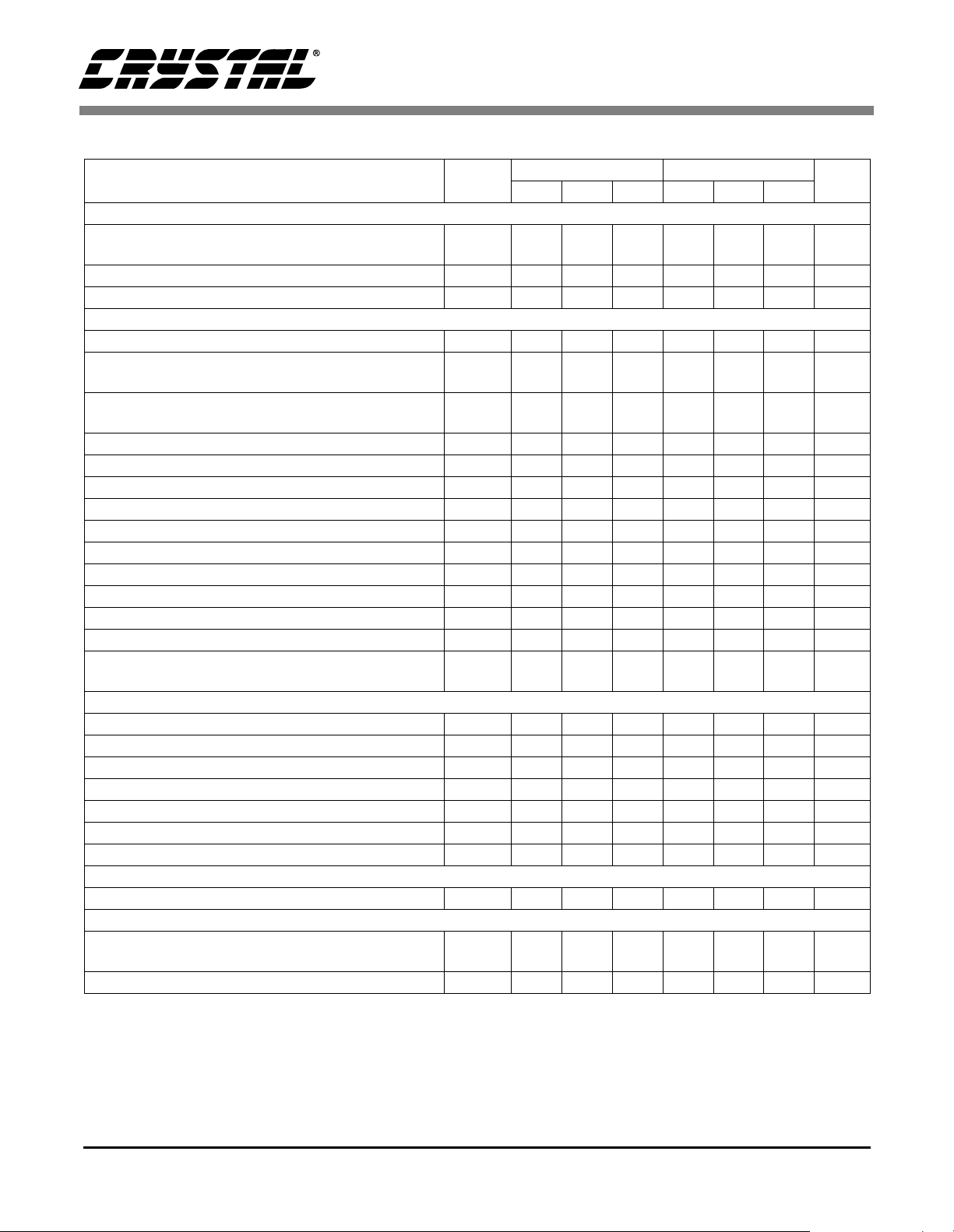
ANALOG CHARACTERISTICS (Continued)
CS4227-KQ CS4227-BQ
Parameter Symbol
High Pass Filter Characteristics
Frequency Response: -3 dB (Note 3)
-0.13 dB
Phase Deviation @ 20 Hz (Note 3) - 10 - - 10 - Deg.
Passband Ripple - - 0 - - 0 dB
Analog Output Characteristics
DAC Resolution 16 - 20 16 - 20 Bits
Signal-to-Noise/Idle (DAC muted, A weighted)
Channel Noise
Dynamic Range (DAC not muted, A weighted)
(DAC not muted, unweighted)
Total Harmonic Distortion THD - 0.003 - - 0.003 - %
Total Harmonic Distortion + Noise (Stereo) THD+N - -88 -83 - -86 -81 dB
Interchannel Isolation - 90 - - 90 - dB
Interchannel Gain Mismatch - 0.1 - - 0.1 - dB
Attenuation Step Size (All Outputs) 0.7 1 1.3 0.7 1 1.3 dB
Programmable Output Attenuation Span -84 -86 - -84 -86 - dB
Offset Voltage (relative to CMOUT) - ±15 - - ±15 - mV
Full Scale Output Voltage 0.92 1.0 1.08 0.92 1.0 1.08 Vrms
Gain Drift - 100 - - 1 00 -
Out-of-Band Energy (Fs/2 to 2Fs) - -60 - - -60 - dBFs
Analog Output Load Resistance:
- Minimum Attenuation, 10 k, 100 pF load; unless otherwise specified.
Capacitance:
-
3.4
-
20
101 108 - 99 106 - dB
93
10
98
-
95
-
-
-
-
-
-
-
-
100
91
10
-
3.4
-
20
96
-
93
-
-
-
100
Combined Digital and Analog Filter Characteristics
Frequency Response 10 Hz to 20 kHz - ±0.1 - - ±0.1 - dB
Deviation from Linear Phase - ±0.5 - - ±0.5 - Deg.
Passband: to 0.01 dB corner (Notes 6, 7) 0 - 20.0 0 - 20.0 kHz
Passband Ripple (Note 7) - - ±0.01 - - ±0.01 dB
Stopband (Notes 6 ,7) 24.1 - - 24.1 - - kHz
Stopband Attenuation (Note 8) 70 - - 70 - - dB
Group Delay (Fs = Input Word Rate) (Note 5) tgd - 16/Fs - - 16/Fs - s
Analog Loopback Performance
Signal-to-noise Ratio (CCIR-2K weighted, -20 dB input)
CCIR-2K
-71- -71-dB
Power Supply
Power Supply Current Operating
Power Down
Power Supply Rejection (1 kHz, 10 mV
Notes: 6. The passband and stopband edges scale with frequency. For input word rates, Fs, other than 44.1 kHz,
the 0.05 dB passband edge is 0.4535xFs and the stopband edge is 0.5465xFs.
7. Digital filter characteristics.
8. Measurement bandwidth is 10 H z to 3Fs.
Specifications are subject to change without notice
) - 45 - - 45 - dB
rms
-
-
901113
3
-
9011153mA
-
-
-
-
-
-
UnitsMin Typ Max Min Typ Max
Hz
Hz
dB
dB
ppm/°C
Ω
k
pF
mA
DS281PP2 5
CS4227
1
384
()
Fs
--------------------- 20+
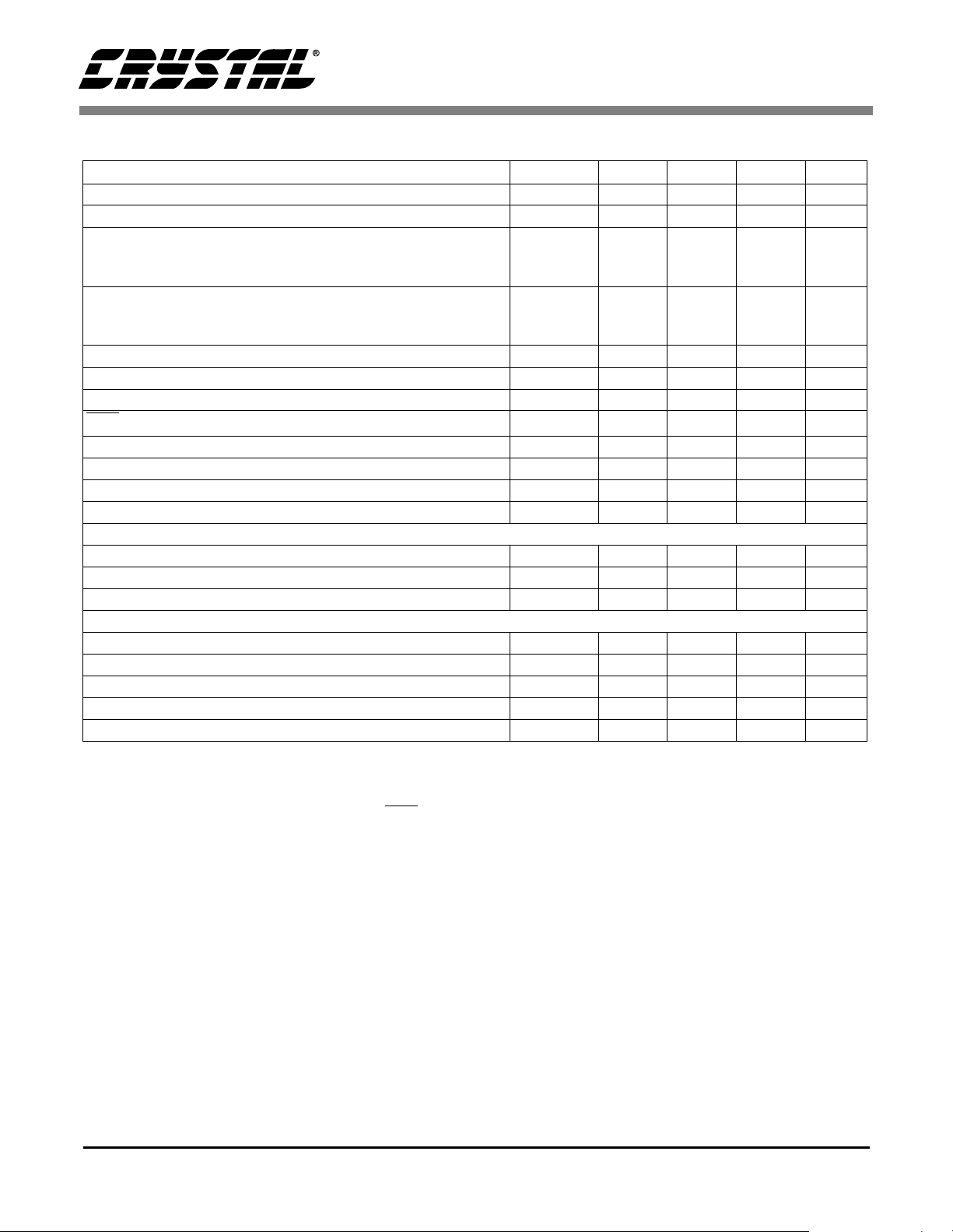
SWITCHING CHARACTERISTICS (T
= 25 °C; VA+, VD+ = +5 V ±5%; outputs loaded with 30 pF.)
A
Parameter Symbol Min Typ Max Unit
Audio ADC’s and DAC’s Sample Rate Fs 4 - 50 kHz
XTI Frequency XTI = 256, 384, or 512 Fs 1.024 - 26 MHz
XTI Pulse Width High XTI = 512 Fs
XTI = 384 Fs
XTI = 256 Fs
XTI Pulse Width Low XTI = 512 Fs
XTI = 384 Fs
XTI = 256 Fs
10
21
31
10
21
31
-
-
-
-
-
-
-
ns
-
-
-
ns
-
XTI Jitter Tolerance - 500 - ps
CLKOUT Jitter (Note 9) - 200 - psRMS
CLKOUT Duty Cycle (high timer/cycle time) (Note 10) 40 50 60 %
PDN
Low Time (Note 11)
SCLK Falling Edge to SDOUT Output Valid DSCK = 0 t
LRCK edge to MSB valid t
SDIN Setup Time Before SCLK Rising Edge DSCK = 0 t
SDIN Hold Time After SCLK Rising Edge DSCK = 0 t
dpd
lrpd
ds
dh
500 - - ns
- - Note 12 ns
- - 40 ns
- - 25 ns
- - 25 ns
Master Mode
SCLK Falling to LRCK Edge DSCK = 0 t
mslr
-±10-ns
SCLK Period (Note 14) - - - - SCLK Duty Cycle - 50 - %
Slave Mode
SCLK Period t
SCLK High Time t
SCLK Low Time t
SCLK Rising to LRCK Edge DSCK = 0 t
LRCK Edge to SCLK Rising DSCK = 0 t
sckw
sckh
sckl
lrckd
lrcks
Note 13 - - ns
40 - - ns
40 - - ns
20 - - ns
40 - - ns
Notes: 9. CLKOUT Jitter is for 256x Fs selected as output frequency measured from falling edge to falling edge.
Jitter is greater for 384x Fs and 512x Fs as selected output frequency.
10. For CLKOUT frequency equal to 1x Fs, 384x Fs, and 512x Fs. See Master Clock Output section.
11. After powering up the CS4227, PDN
should be held low for 1 ms to allow the power supply to settle.
12.
13.
14.
1
---------------------
()
128
Fs
1
-------------------
256()
Fs
6 DS281PP2
SCLK*
SCLKAUX*
(output)
LRCK
LRCKAUX
(output)
SDOUT1
SDOUT2
Figure 1. Audio Ports Master Mode Timing
LRCK
LRCKAUX
(input)
t
lrckd
t
lrcks
t
sckh
t
mslr
t
sckl
CS4227
SCLK*
SCLKAUX*
(input)
SDIN1
SDIN2
SDIN3
DATAUX
SDOUT1
SDOUT2
*SCLK, SCLKAUX shown for DSCK = 0 and ASCK = 0.
SCLK & SCLKAUX inverted for DSCK = 1 and ASCK = 1, respectively.
t
lrpd
t
ds
MSB
t
sckw
t
dh
t
dpd
MSB-1
Figure 2. Audio Ports Slave Mode and Data I/O Timing
DS281PP2 7
CS4227
SWITCHING CHARACTERISTICS - CONTROL PORT (T
Inputs: logic 0 = DGND, logic 1 = VD+; C
= 30 pF)
L
= 25 °C; VA +, VD+ = +5 V ± 5 %;
A
Parameter Symbol Min Max Unit
SPI Mode (SPI/I2C = 0)
CCLK Clock Frequency f
CS
High Time Between Transmissions
CS
Falling to CCLK Edge
CCLK Low Time t
CCLK High Time t
CDIN to CCL Rising Setup Time t
CCLK Rising to DATA Hold Time (Note 15) t
CCLK Falling to CDOUT stable t
Rise Time of CDOUT t
Fall Time of CDOUT t
Rise Time of CCLK and CDIN (Note 16) t
Fall Time of CCLK and CDIN (Note 16) t
t
t
sck
csh
css
scl
sch
dsu
dh
pd
r1
f1
r2
f2
-6MHz
1.0 - µs
20 - ns
66 - ns
66 - ns
40 - ns
15 - ns
-45ns
-25ns
-25ns
- 100 ns
- 100 ns
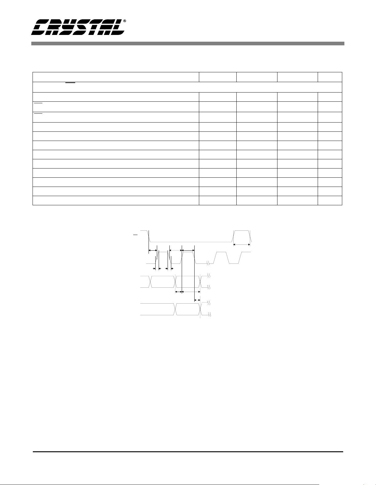
Notes: 15. Data must be held for sufficient time to bridge the transition time of CCLK.
16. For F
< 1 MHz.
SCK
CS
CCLK
CDIN
CDOUT
t
css
t
r2
t
t
scl
sch
t
f2
t
t
dsu
dh
Figure 3. Control Port SPI Mode
t
csh
t
pd
8 DS281PP2

CS4227
SWITCHING CHARACTERISTICS - CONTROL PORT (T
Inputs: logic 0 = DGND, logic 1 = VD+; C
Parameter Symbol Min Max Unit
I2C® Mode (SPI/I2C = 1) (Note 17)
SCL Clock Frequency f
Bus Free Time Between Transmissions t
Start Condition Hold Time (prior to first clock pulse) t
Clock Low Time t
Clock High Time t
Setup Time for Repeated Start Condition t
SDA Hold Time for SCL Falling (Note 18) t
SDA Setup Time to SCL Rising t
Rise Time of Both SDA and SCL Lines t
Fall Time of Both SDA and SCL Lines t
Setup Time for Stop Condition t
2C®
Notes: 17. I
is a registered trademark of Philips Semiconductors.
18. Data must be held for sufficient time to bridge the 300 ns transition time of SCL.
Stop Start
= 30 pF)
L
scl
buf
hdst
low
high
sust
hdd
sud
r
f
susp
Repeated
Start
= 25 °C; VA+, VD+ = +5 V ± 5 %;
A
-100kHz
4.7 - µs
4.0 - µs
4.7 - µs
4.0 - µs
4.7 - µs
0-µs
250 - ns
-1µs
- 300 ns
4.7 - µs
Stop
SDA
SCL
t
buf
t
hdst
t
low
t
high
t
hdd
t
sud
t
sust
t
hdst
t
f
t
r
t
susp
Figure 4. Control Port I2C Mode
DS281PP2 9
CS4227
ABSOLUTE MAXIMUM RATINGS (AGND, DGND = 0 V, all voltage with respect to 0 V.)
Parameter Symbol Min Max Unit
Power Supplies Digital
Analog
Input Current (Note 19) - ±10 mA
Analog Input Voltage (Note 20) -0.7 (VA+) + 0.7 V
Digital Input Voltage (Note 20) -0.7 (VD+) + 0.7 V
Ambient Temperature (Power Applied) -55 +125 °C
Storage Temperature -65 +150 °C
Notes: 19. Any pin except supplies. Transient currents of up to ±100 mA on the analog input pins will not cause
SCR latch-up.
20. The maximum over or under voltage is limited by the input current.
WARNING: WARNING:Operation at or beyond these limits may result in permanent damage to the device.
Normal operation is not guaranteed at these extremes.
RECOMMENDED OPERATING CONDITIONS (AGND, DGND = 0 V, all voltage with respect to
0 V.)
VD+
VA+
-0.3
-0.3
6.0
6.0
V
Parameter Symbol Min Typ Max Unit
Power Supplies Digital
|VA+ - VD+| < 0.4 V Analog
Operating Ambient Temperature T
DIGITAL CHARACTERISTICS (T
Parameter Symbol Min Max Unit
High-level Input Voltage (Except XTI) V
Low-level Input Voltage (Except XTI) V
High-level Output Voltage (Except XTO) V
Low-level Out put Voltage (Except XTO) V
Input Leakage Current (Digital Inputs) - 10 µA
Output Leakage Current (High-Impedance Digital Outputs) - 10 µA
= 25 °C; VA+, VD+ = +5 V ±5%)
A
VD+
VA+
A
IH
IL
OH
OL
4.75
4.75
-10 25 70 °C
2.8 (VD+) + 0.3 V
-0.3 0.8 V
(VD+) - 1.0 - V
5.0
5.0
-0.4V
5.25
5.25
V
10 DS281PP2
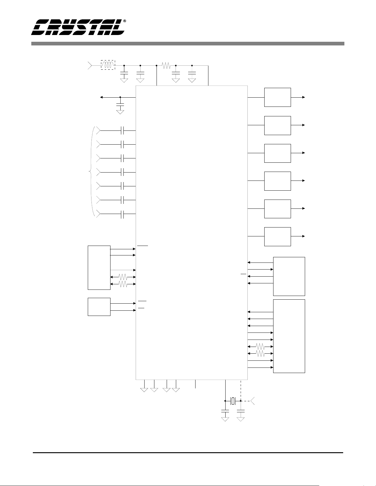
CS4227
+5V
Supply
To Optional
Input and
Output Buffers
From Optional Input Buffer
Digital
Audio
Source
Ferrite Bead
1
F
µ
10 µF
10 µF
10 µF
10 µF
10 µF
µ
10
10 µF
R
R
1 µF 0.1 µF
+
+
*
*
*
*
*
F
*
*
S
S
16
14
13
11
12
10
9
15
27
2
1
44
43
2.0
Ω
+
19
VA+ VD+
CMOUT
AIN1L
AIN1R
AIN2L
AIN2R
AIN3L
AIN3R
AINAUX
DEM
HOLD
DATAUX
LRCKAUX
SCLKAUX
1 µF 0.1 µF
CS4227
40
AOUT1
AOUT2
AOUT3
AOUT4
AOUT5
AOUT6
SCL/CCLK
SDA/CDOUT
AD0/CS
AD1/CDIN
21
ANALOG
FILTER
22
ANALOG
FILTER
23
ANALOG
FILTER
24
ANALOG
FILTER
25
ANALOG
FILTER
26
ANALOG
FILTER
3
4
6
5
Microcontroller
8
Mode
Setting
R = 50
Ω
S
All unused digital inputs
should be tied to 0V.
Unused analog inputs
should be left unconnected.
* Optional if analog inputs biased
to within 1% of CMOUT
PDN
7
SPI/I2C
AGND1, 2 DGND1, 2 NC XTO XTI
39412018
17
29 28
SDIN1
SDIN2
SDIN3
SDOUT1
SDOUT2
LRCK
SCLK
CLKOUT
OVL
C1** C2**
34
33
32
36
35
37
38
31
30
External
Clock Input
Audio
R
R
DSP
S
S
Figure 5. Recommended Connection Diagram
(Also see recommended layout diagrams, Figure 14)
DS281PP2 11

2. FUNCTIONAL DESCRIPTION
CS4227
2.1 Overview
The CS4227 has 2 channels of 20-bit analog-todigital conversion and 6 channels of 20-bit digitalto-analog conversion. A mono 20-bit ADC is also
provided. All ADCs and DACs are delta-sigma
converters. The stereo ADC inputs have adjustable
input gain, while the DAC outputs have adjustable
output attenuation.
Digital audio data received by the DACs and transmitted from the ADCs is communicated over separate serial ports, allowing concurrent writing to and
reading from the device. The CS4227 functions are
controlled via a serial microcontroller interface.
Figure 1 shows the recommended connection diagram for the CS4227.
2.2 Analog Inputs
2.2.1 Line Level Inputs
AIN1R, AIN1L, AIN2R, AIN2L, AIN3R, AIN3L
and AINAUX are the line level input pins (See Figure 5). These pins are internally biased to the
CMOUT voltage (nominally 2.3 V). A 10 µ F DC
blocking capacitor allows signals centered around
0 V to be input. Figure 6 shows an optional dual op
amp buffer which combines level shifting with a
gain of 0.5 to attenuate the standard line level of
2V
used to bias the op-amps to approximately one half
the supply voltage. With this input circuit, the
10 µF DC blocking caps in Figure 5 may be omitted. Any remaining DC offset will be removed by
the internal high-pass filters.
Selection of the stereo input pair for the 20-bit
ADC's is accomplished by setting the AIS1/0 bits,
which are accessible in the ADC Control Byte. Onchip anti-aliasing filters follow the input mux, providing anti-aliasing for all input channels.
rms
to 1 V
. The CMOUT reference level is
rms
100 pF
Line In
Right
Example
Op-Amps are
MC34074 or
MC33078
Line In
Left
Figure 6. Optional Line Intput Buffer
3.3 µF
3.3 µF
20 k
0.47 µF
20 k
-
+
+
-
10 k
AINxR
5 k
CMOUT
AINxL
10 k
100 pF
The analog inputs may also be configured as differential inputs. This is enabled by setting bits
AIS1/0 = 3. In the differential configuration, the
left channel inputs reside on pins 10 and 11, and the
right channel inputs reside on pins 12 and 13 as described in the table below. In differential mode, the
full scale input level is 2 V
Single-ended Pin # Differential Inputs
AIN3L Pin 10 AINL+
AIN3R Pin 9 unused
AIN2L Pin 11 AINLAIN2R Pin 12 AINRAIN1L Pin 14 unused
AIN1R Pin 13 AINR+
Table 1. Single-ended vs Differential Input Pin
Assignments
rms
.
The analog signal is input to the mono ADC via the
AINAUX pin.
Independent Muting of both the stereo ADC's and
the mono ADC is possible through the ADC Control Byte (#11) with the MUTR, MUTL and
MUTM bits.
12 DS281PP2

CS4227
2.2.2 Adjustable Input Gain
The signals from the line inputs are routed to a programmable gain circuit which provides up to 9 dB
of gain in 3 dB steps, adjustable through the Input
Control Byte. Right and left channel gain settings
are controlled independently with the GNR1/0 and
GNL1/0 bits. To minimize audible artifacts, level
changes should be done with the channel muted, as
the changes occur immediately on register updates.
The ADC Status Report Byte provides feedback of
input level for each ADC channel. This register
continously monitors the ADC output and records
the peak output level since the last register read.
Reading this register causes it to reset to 0, whereupon peak monitoring begins again.
2.2.3 High Pass Filter
The operational amplifiers in the input circuitry
driving the CS4227 may generate a small DC offset
into the A/D converter. The CS4227 includes a
high pass filter after the decimator to remove any
DC offset which could result in recording a DC level, possibly yielding "clicks" when switching between devices in a multichannel system.
The characteristics of this first-order high pass filter are outlined below for an output sample rate of
44.1 kHz. This filter response scales linearly with
sample rate.
2.3 Analog Outputs
2.3.1 Line Level Outputs
The CS4227 contains an on-chip buffer amplifier
producing single-ended outputs capable of driving
10 kΩ loads. Each output (AOUT 1-6) will produce
a nominal 2.83 Vpp (1 V
quiescent voltage for a full scale digital input. The
recommended off-chip analog filter is a 2nd order
Butterworth with a -3 dB corner at Fs (see
Figure 7). This filter provides out-of-band noise attenuation along with a gain of 2, providing a 2 V
output signal. A 3rd order Butterworth filter with a
-3 dB corner at 0.75 Fs can be used if greater out of
band noise filtering is desired. The CS4227 DAC
interpolation filter is a linear phase design which
has been pre-compensated for an external 2nd order Butterworth filter to provide a flat frequency response and linear phase response over the
passband. If this filter is not used, small frequency
response magnitude and phase errors will occur.
22 k
3.9 k
Ω
1000pF
C
11 k
MOUT
) output with a 2.3 volt
rms
150pF
Ω
Ω
5 k
_
+
Example
Op-Amps
Ω
MC33078
0.47 µF
are
rms
Frequency Response -3dB @ 3.4 Hz
2-Pole Butterworth Filter
-0.13 dB @ 20 Hz
Phase Deviation 10 degrees @ 20 Hz
1.21 k
5 k
560 pF
Ω
Ω
_
+
Ω
0.47 µF
Passband Ripple None
Table 2. High Pass Filter Characteristics
A
OUT
5600 pF
5.85 k
1.1 k
Ω
4.75 k
Ω
5600 pF
C
MOUT
3-Pole Butterworth Filter
Figure 7. Butterworth Filters
DS281PP2 13

CS4227
2.3.2 Output Level Attenuator
The DAC outputs are each routed through an attenuator which is adjustable in 1 dB steps. Output attenuation is available through the Output
Attenuator Data Bytes. Level changes are implemented such that the noise is attenuated by the
same amount as the signal (equivalent to using an
analog attenuator after the signal source) until the
residual output noise is equal to the noise floor in
the mute state. Level changes only take effect on
zero crossings to minimize audible artifacts. If
there is no zero crossing, then the requested level
change will occur after a time-out period between
512 and 1024 frames (11.6 ms to 23.2 ms at
44.1 kHz frame rate). There is a separate zero
crossing detector for each channel. Each A CC bit
in the DAC Status Report Byte provides information on when a volume control change has taken effect. This bit goes high when a new setting is
loaded and returns low when it has taken effect.
Volume control changes can be instantaneous by
setting the Zero Crossing Disable (ZCD) bit in the
DAC Control Byte (#3) to 1.
Each output can be independently muted via mute
control bits, MUT6-1, in the DAC Control Byte
(#3). The mute also takes effect on a zero-crossing
or after a timeout. In addition, the CS4227 has an
optional mute on consecutive zeros feature, where
all DAC outputs will mute if they receive between
512 and 1024 consecutive zeros (or -1 code) on all
six channels. A single non-zero value will unmute
the DAC outputs. This feature can be disabled with
the MUTC bit in the DAC Control Byte (#3).
2.4 Clock Generation
The master clock to operate the CS4227 may be
generated by using the on-chip inverter and an external crystal or by using an external clock source.
If the active clock source stops for 10 µs, the
CS4227 will enter a power down state. In all modes
it is required to have SCLK and LRCK synchronous to the selected master clock.
2.4.1 Clock Source
The CS4227 requires a high frequency master
clock to run the internal logic. The clock enable bit
(CE) must be set to 0 after power-up of the device
(see Power-up/Reset/Power Down Mode section).
A high frequency crystal can be connected to XTI
and XTO, or a high frequency clock can be applied
to XTI. This high frequency clock can be 256 Fs,
384 Fs or 512 Fs; this is set by the CI0/1 bits in the
Clock Mode Byte (#1). When using the on-chip
crystal oscillator, external loading capacitors are
required (see Figure 5). High frequency crystals
(>8 MHz) should be parallel resonant, fundamental
mode and designed for 20 pF loading (equivalent to
40 pF to ground on each leg).
2.4.2 Master Clock Output
CLKOUT is a master clock output provided to allow synchronization of external components.
Available CLKOUT frequencies of 1 Fs, 256 Fs,
384 Fs, and 512 Fs, are selectable by the CO0/1 bits
of the Clock Mode Byte.
Generation of CLKOUT for 384 Fs and 512 Fs is
accomplished with an on chip clock multiplier and
may contain clock jitter. The source of the 256 Fs
CLKOUT is a divided down clock from the
XTI/XTO input. If 384 Fs is chosen as the input
clock at XTI and 256 Fs is chosen as the output,
CLKOUT will have approximately a 33% duty cycle. In all other cases CLKOUT will typically have
a 50% duty cycle.
2.4.3 Synchronization
The DSP port and Auxiliary port must operate synchronously to the CS4227 clock source. The serial
port will force a reset of the data paths in an attempt
to resynchronize if non-synchronous data is input
to the CS4227. It is advisable to mute the DACs
when changing from one clock source to another to
avoid the output of undesirable audio signals as the
CS4227 resynchronizes.
14 DS281PP2

CS4227
2.5 Digital Interfaces
There are 2 digital audio interface ports: the audio
DSP port and the auxiliary digital audio port. The
serial data is represented in 2’s complement format
with the MSB-first in all formats.
2.5.1 Audio DSP Serial Interface Signals
The serial interface clock, SCLK, is used for transmitting and receiving audio data. The active edge
of SCLK is chosen by setting the DSCK bit in the
DSP Port Mode Byte (#14). SCLK can be generated by the CS4227 (master mode) or it can be input
from an external SCLK source (slave mode). Mode
selection is set with the DMS1/0 bits in the DSP
Port Mode Byte (#14). The number of SCLK cycles in one system sample period is programmable
to be 32, 48, 64, or 128 by setting the DCK1/0 bits
in the DSP Port Mode Byte (#14). When SCLK is
an input, 64 SCLK’s per system sample period is
not recommended, due to potential interference effects; if possible 128 SCLK’s per sample period
should be used instead. For master mode, bursting
of a 128 Fs clock is preferrable over evenly distributed clocks.
The Left/Right clock (LRCK) is used to indicate
left and right data and the start of a new sample period. It may be output from the CS4227, or it may
be generated from an external controller. The frequency of LRCK must be equal to the system sample rate, Fs.
SDIN1, SDIN2, and SDIN3 are the data input pins,
each of which drives a pair of DACs. SDOUT1 and
SDOUT2 can carry the output data from the two
20-bit ADC’s, the mono ADC and the auxiliary digital audio port. Selection depends on the IS1/0 bits
in the ADC control byte (#11). The audio DSP port
may also be configured so that all 6 DAC’s data is
input on SDIN1, and all 3 ADC’s data is output on
SDOUT1. Table 3 outlines the serial interface
ports.
DAC Inputs
SDIN1 left channel
right channel
single line
SDIN2 left channel
right channel
SDIN3 left channel
right channel
Table 3. DSP Serial Input Ports
DAC #1
DAC #2
All 6 DAC channels
DAC #3
DAC #4
DAC #5
DAC #6
2.5.2 Audio DSP Serial Interface Formats
The audio DSP port supports 7 alternate formats,
shown in Figures 8, 9, and 10. These formats are
chosen through the DSP Port Mode Byte (#14) with
the DDF2/1/0 bits.
Formats 5 and 6 are single line data modes where
all DAC channels are combined onto a single input
and all ADC channels are combined onto a single
output. Format 6 is available in master mode only.
See Figure 10.
2.5.3 Auxiliary Audio Port Signals
The auxiliary port provides an alternate way to input digital audio signals into the CS4227. This port
consists of clock, data and left/right clock pins
named, SCLKAUX, DATAUX and LRCKAUX.
The Auxiliary Audio Port input is output on
SDOUT1 when IS is set to 1 or 2 in the ADC Control Byte. Additionally, setting IS to 2 routes the
stereo ADC outputs to SDOUT2. There is approximately a two frame delay from DATAUX to
SDOUT1. When the auxiliary port is used, the frequency of LRCKAUX must be equal to the system
sample rate, Fs, but no particular phase relationship
is required.
De-emphasis can be performed on input data to the
auxiliary audio port; this is controlled by the Auxiliary Port Control Byte (#16).
2.5.4 Auxiliary Audio Port Formats
Input data on DATAUX is clocked into the part by
SCLKAUX using the format selected in the Auxiliary Port Mode Byte. The auxiliary audio port sup-
DS281PP2 15

CS4227
FORMAT 0, 1, 2:
Format 0: M = 20
Format 1: M = 18
Format 2: M = 16
FORMAT 3:
FORMAT 4:
Note: SCLK shown for DSCK = 0. SCLK inverted for DSCK = 1.
Figure 8. Audio DSP and Auxiliary Port Data Input Formats
FORMAT 0, 1, 2:
Format 0: M = 20
Format 1: M = 18
Format 2: M = 16
FORMAT 3:
LRCK
Left Right
SCLK
SDIN
LRCK
SCLK
LSB LSBMSB LSBMSB
Left Right
SDIN MSB LSB
LRCK
SCLK
SDIN
LRCK
Left Right
MSB LSB
Left Right
SCLK
SDOUT
LRCK
SCLK
LSB LSBMSB LSBMSB
Left Right
SDOUT MSB LSB
M SCLKs
M SCLKs
M SCLKs
MSB LSB MSB
MSB LSB
M SCLKs
MSB LSB MSB
FORMAT 5:
FORMAT 6:
(Master Mode Only)
FORMAT 4:
LRCK
SCLK
SDIN1
SDOUT1
LRCK
SCLK
SDIN1
SDOUT1
LRCK
SCLK
SDOUT
Left Right
MSB LSB
MSB LSB
Note: SCLK s h own for DSCK = 0. SCLK inverted for DSCK = 1.
Figure 9. Audio DSP Port Data Output Formats
64 SCLKS 64 SCLKS
LSBMSB
DAC #1 DAC #3 DAC #5 DAC #2 DAC #4 DAC #6
20 clks
SDOUT1 SDOUT2 SDOUT1 SDOUT2
20 clks
LSBMSB
DAC #1
32 clks
SDOUT1 SDOUT2
32 clks
LSBMSB LSBMSB LSBMSB LSBMSB LSBMSB MSB
20 clks 20 clks 20 clks
20 clks 20 clks
128 SCLKS 128 SCLKS
LSBMSB
DAC #3
32 clks
32 clks
LSBMSB
DAC #5
32 clks
20 clks
20 clks
LSBMSB
DAC #2
32 clks
SDOUT1
32 clks
Figure 10. One Data Line Modes
20 clks
LSBMSB LSBMSB
DAC #4 DAC #6
32 clks
SDOUT2
32 clks
32 clks
16 DS281PP2

CS
CCLK
CDIN
CHIP
ADDRESS
0010000
R/W
MAP
MSB
byte 1
DATA
LSB
byte n
CHIP
ADDRESS
0010000
CS4227
R/W
CDOUT
MAP = Memory Address Pointer
Figure 11. Control Port Timing, SPI Mode
ports the same 5 formats as the audio DSP por t in
multi-data line mode. LRCKAUX is used to indicate left and right data samples, and the start of a
new sample period. SCLKAUX and LRCKAUX
may be output from the CS4227, or they may be
generated from an external source, as set by the
AMS1/0 control bits in the Auxiliary Port Mode
Byte (#15).
2.6 Control Port Signals
The control port is used to load all the internal settings. The operation of the control port may be
completely asynchronous with the audio sample
rate. However, to avoid potential interference problems, the control port pins should remain static if
no operation is required.
The control port has 2 modes: SPI and I2C®, with
the CS4227 as a slave device. The SPI mode is selected by setting the SPI/I2C pin low, and I2C® is
selected by setting the SPI/I2C pin high. The state
of this pin is continuously monitored.
2.6.1 SPI Mode
In SPI mode, CS is the CS4227 chip select signal,
CCLK is the control port bit clock, (input into the
CS4227 from the microcontroller), CDIN is the input data line from the microcontroller, CDOUT is
the output data line to the microcontroller, and the
chip address is 0010000. Data is clocked in on the
rising edge of CCLK and out on the falling edge.
High Impedance
MSB
LSB
MSB
LSB
Figure 11 shows the operation of the control port in
SPI mode. To write to a register, bring CS low. The
first 7 bits on CDIN form the chip address, and they
must be 0010000. The eighth bit is a read/write indicator (R/W), which should be low to write. The
next 8 bits form the Memory Address Pointer
(MAP), which is set to the address of the register
that is to be updated. The next 8 bits are the data
which will be placed into register designated by the
MAP. During writes, the CDOUT output stays in
the high impedance state. It may be externally
pulled high or low with a 47 kΩ resistor.
The CS4227 has a MAP auto increment capability,
enabled by the INCR bit in the MAP register. If
INCR is a zero, then the MAP will stay constant for
successive reads or writes. If INCR is set to a 1,
then MAP will auto increment after each byte is
read or written, allowing block reads or writes of
successive registers.
To read a re gister, t he MAP has to be set to the co rrect address by executing a partial write cycle
which finishes (CS high) immediately after the
MAP byte. The auto MAP increment bit (INCR)
may be set or not, as desired. To begin a read, bring
CS low, send out the chip address and set the
read/write bit (R/W) high. The next falling edge of
CCLK will clock out the MSB of the addressed
register (CDOUT will leave the high impedance
state). If the MAP auto incr ement bit is set to 1, the
data for successive registers will appear consecutively.
DS281PP2 17

SDA
SCL
00100
ADDR
AD1-0
R/W
ACK
DATA
1-8
Note 1
ACK
DATA
1-8
CS4227
ACK
Start
Note 1: If operation is a write, t his byte contains the Memor y Address Pointe r , MAP.
Figure 12. Control Port Timing, I2C® Mode
2.6.2 I2C® Mode
In I2C® mode, SDA is a bidirectional data line.
Data is clocked into and out of the part by the clock,
SCL, with the clock to data relationship as shown
in Figure 12. There is no CS pin. Pins AD0, AD1
form the partial chip address. The upper 5 bits of
the 7 bit address field must be 00100. To communicate with a CS4227, the LSBs of the chip address
field, which is the first byte sent to the CS4227,
should match the settings of the AD1, AD0 pins.
The eighth bit of the address bit is the R/W bit (high
for a read, low for a write). If the operation is a
write, the next byte is the Memory Address Pointer
which selects the register to be read or written. If
the operation is a read, the contents of the register
pointed to by the Memory Address Pointer will be
output. Setting the auto increment bit in MAP, allows successive reads or writes of consecutive registers. Each byte is separated by an acknowledge
bit. Use of the I2C bus® compatible interface requires a license from Philips. I2C bus® is a registered trademark of Philips Semiconductors.
Stop
2.7 Power-up/Reset/Power Down Mode
Upon power up, the user should hold PDN = 0 for
approximately 1ms. In this state, the control port is
reset to its default settings. At the end of the PDN,
the device remains in a low power mode in which
CMOUT will not supply current, but the control
port is active. The desired settings should be loaded
while keeping the RS bit set to 1. Normal operation
is achieved by setting the CE bit to zero in the
Clock Mode Byte (#1) and the RS bit to zero i n the
Converter Control Byte (#2). Once done, the part
powers up and an offset calibration occurs. This
process lasts approximately 50 ms.
Reset/power down is achieved by lowering the
PDN pin causing the part to enter power down.
Once PDN goes high, the control port is functional
and the desired settings should be loaded in while
keeping the RS bit set to 1. The remainder of the
chip remains in a low power reset stat e until the RS
bit in the Convertor Control Byte is set to 0. After
clearing the RS bit, the CE bit (Clock Enable) in the
Clock Mode Byte (#1) should also be set to zero.
2.6.3 Control Port Bit Definitions
The CS4227 will also enter a stand by mode if the
master clock source stops for approximately 10 µs
All registers can be written and read ba ck, except
the DAC Status Report Byte (#10) and ADC Status
Report Byte (#13), which are read only. See the fol-
or if the LRCK is not synchronous to the master
clock. The control port will retain its current settings.
lowing bit definition tables for bit assignment information.
18 DS281PP2

2.8 DAC Calibration
Output offset voltage is minimized by an internal
calibration cycle. A calibration will automatically
occur anytime the part comes out of reset, including the power-up reset, or when the master clock
source to the part changes by changing the CE or CI
bits in the Clock Mode Byte.
The CS4227 can be re-calibrated whenever desired. A control bit, CAL, in the Converter Control
Byte, is provided to initiate a calibration. The sequence is:
1) Set CAL to 1, the CS4227 sets CALP to 1 and
begins to calibrate.
2) CALP will go to 0 when the calibration is completed.
Additional calibrations can be implemented by setting CAL to 0 and then to 1.
2.9 De-Emphasis
The CS4227 is capable of digital de-emphasis for
32, 44.1, or 48 kHz sample rates. Implementation
of digital de-emphasis requires reconfiguration of
the digital filter to maintain the filter response
shown in Figure 13 at multiple sample rates. The
Auxiliary Port Control Byte selects the de-emphasis control method. De-emphasis may be enabled
under hardware control, using the DEM pin
(DEM2/1/0=4,5,6), or by software control using
the DEM bit (DEM2/1/0=0,1,2,3)
2.10 Hold Function
If the digital audio source presents invalid data to
the CS4227, the CS4227 may be configured to
cause the last valid digital input level to be held
constant (this sounds much better than a potentially
random output level). Holding the previous output
sample occurs when the user asserts the HOLD pin
(HOLD = 1) at any time during the stereo sample
period. During a HOLD condition, AUXPort input
data is ignored. DAC outputs can be automatically
muted after an extended HOLD period (>15 sam-
CS4227
Gain
dB
µ
T1=50
0dB
-10dB
Figure 13. De-emphasis Curve.
ples) by setting the MOH bit = 0 in the Auxiliary
Port Control Byte. DACs will not be automatically
muted when MOH = 1. When the HOLD pin is deasserted (HOLD = 0), the DAC outputs will return
to one of two different states controlled by the
UMV (Unmute on Valid Data) bit in the Auxiliary
Port Control Byte. When UMV = 0, the DAC outputs will unmute when the HOLD is removed.
When UMV = 1, the DACs must be unmuted in the
DAC Control Byte after the HOLD is removed.
This allows the user to unmute the DAC after the
invalid data has passed through the DSP.
2.11 Power Supply, Layout, and Grounding
The CS4227, along with associated analog circuitry, should be positioned near the split between
ground planes, and have its own, separate, ground
plane (see Figure 14). Preferably, it should also
have its own power plane. The +5 V supply must be
connected to the CS4227 via a ferrite bead, positioned closer than 1" to the device. A single connection between the CS4227 ground and the board
ground should be positioned as shown in Figure 14.
The location of the 1 µF CMOUT filtering capicator should be as close to the CS4227 as possible.
See Crystal's layout Applications Note, and the
CDB4227 evaluation board data sheet for recommended layout of the decoupling components.
s
F1 F2
T2 = 15
Frequency
µ
s
DS281PP2 19

The CS4227 will mute the analog outputs and enter
the Power Down Mode if the supply drops below
approximately 4 volts.
2.12 ADC and DAC Filter Response Plots
Figures 15 through 20 show the overall frequency
response, passband ripple and transition band for
the CS4227 ADC’s and DAC’s.
CS4227
1/8">
Digital
Ground
Plane
CPU & Digital
Logic
+5V
Ferrite
Bead
Ground
Connection
CS4227
Codec
digital
signals
Analog
Ground
Plane
Codec
analog
signals &
components
Note that the CS4227
is oriented with its
digital pins towards the
digital end of the board.
Figure 14. Suggested Layout Guideline
20 DS281PP2

Figure 15. 20-bit ADC Filter Response Figure 16. 20-bit ADC Passband Ripple
CS4227
Figure 17. 20-bit ADC Transition Band Figure 18. DAC Frequency Response
Figure 19. DAC Passband Ripple Figure 20. DAC Transition Band
DS281PP2 21

CS4227
2.13 Memory Address Pointer (MAP)
76543210
INCR 0 0 MAP4 MAP3 MAP2 MAP1 MAP0
MAP4-MAP0 Register Pointer
INCR Auto Increment Control Bit
0 - No auto increment
1 - Auto increment on
This register defaults to 01h.
2.14 Reserved Byte (0)
This byte is reserved for internal use and must be set to 00h for normal operation.
This register defaults to 00h.
2.15 Clock Mode Byte (1)
76543210
0CO1CO0CI1CI00 0 CE
CE Master clock enable
0 - Clock Enabled
1 - Clock Disabled
CI1-CI0 Determines frequency of XTI
0 - 256 Fs
1 - 384 Fs
2 - 512 Fs
3 - not used
CO1-CO0 Se ts CLK OUT freque nc y
0 - 256 Fs
1 - 384 Fs
2 - 512 Fs
3 - 1 Fs
This register defaults to 01h.
22 DS281PP2

CS4227
2.16 Converter Control Byte (2)
76543210
CALP CLKE DU 0 0 0 CAL RS
RS Chip reset
0 - No Reset
1 - Reset
CAL Calibration control bit
0 - Normal operation
1 - Rising edge initiates calibration
The following bits are read only:
DU Shows selected De-Emphasis setting used by DAC’s
0 - Normal Flat DAC frequency response
1 - De-Emphasis selected
CLKE Clocking system status
0 - No errors
1 - Crystal is not oscillating, or requesting clock change in progress
CALP Calibration status
0 - Calibration done
1 - Calibration in progres
This register defaults to 01h.
2.17 DAC Control Byte (3)
76543210
ZCD MUTC MUT6 MUT5 MUT4 MUT3 MUT2 MUT1
MUT6-MUT1 Mute control bits
0 - Normal output level
1 - Selected DAC output muted
MUTC Controls mute on consecutive zeros function
0 - 512 consecutive zeros will mute DAC
1 - DAC output will not mute on zeros
ZCD Zero crossing disable
0 - DAC mutes and volume control changes occur on zero-crossings
1 - DAC mutes and volume control changes occur immediately.
This register defaults to 3Fh.
DS281PP2 23

CS4227
2.18 Output Attenuator Data Byte (4, 5, 6, 7, 8, 9)
76543210
0 ATT6 ATT5 ATT4 ATT3 ATT2 ATT1 ATT0
ATT6-ATT0 Sets attenuator leve l
0 - No attenuation
127 - 127 dB attenuation
ATT0 represents 1.0 dB of attenuation
This register defaults to 7Fh.
2.19 DAC Status Report Byte (Read Only) (10)
76543210
0 - ACC6 ACC5 ACC4 ACC3 ACC2 ACC1
ACC6-ACC1 Acceptance Bit
0 - ATT6-ATT0 has been accepted.
1 - New setting is waiting for zero-crossing to be accepted.
This register is read-only.
2.20 ADC Control Byte (11)
76543210
IS1 IS0 0 AIS1 AIS0 MUTM MUTR MUTL
MUTL, MUTR, MUTM - Left, right and mono channel mute control
0 - Normal output level
1 - Selected ADC output muted
AIS1-AIS0 ADC analog input mux control
0 - Selects stereo pair 1
1 - Selects stereo pair 2
2 - Selects stereo pair 3
3 - Differential Input
IS1-IS0 Input mux selection
0 - Stereo ADC output to SDOUT1, Mono ADC output to SDOUT2
1 - Auxiliary Digital Input Port to SDOUT1, Mono ADC output to SDOUT2
2 - Auxiliary Digital Input Port to SDOUT1, Stereo ADC output to SDOUT2
3 - Not used.
This register defaults to 00h.
24 DS281PP2

CS4227
2.21 Input Control Byte (12)
76543210
OVRM 0 0 0 GNR1 GNR0 GNL1 GNL0
GNL1-GNL0 Sets left input gain
0 - 0 dB
1 - 3 dB
2 - 6 dB
3 - 9 dB
GNR1-GNR0 Sets right input gain
0 - 0 dB
1 - 3 dB
2 - 6 dB
3 - 9 dB
OVRM ADC Overflow Mask
This register defaults to 00h.
2.22 ADC Status Report Byte (Read Only) (13)
76543210
LVM1 LVM0 LVR2 LVR1 LVR0 LVL2 LVL1 LVL0
LVL2-LVL0, LVR2-0Left and Right ADC output level
0 - Normal output levels
1 - -6 dB level
2 - -5 dB level
3 - -4 dB level
4 - -3 dB level
5 - -2 dB level
6 - -1 dB level
7 - Clipping
LVLM1-LVLM0 Mono ADC output level
0 - Normal output level
1 - -6 dB level
2 - -3 dB level
3 - Clipping
These bits are ’sticky’. They constantly monitor the ADC output for the peak levels and hold the maximum output. They are reset to 0 when read.
This register is read only.
DS281PP2 25

CS4227
2.23 DSP Port Mode Byte (14)
76543210
DCK1 DCK0 DMS1 DMS0 DSCK DDF2 DDF1 DDF0
DDF2-DDF0 Data format
0 - Right justified, 20-bit
1 - Right justified, 18-bit
2 - Right justified, 16-bit
3 - Left justified, 20-bit in / 24-bit out
2
4 - I
S compatible, 20-bit in / 24-bit out
5 - One Data Line Mode (Figure 10)
6 - One Data Line (Master Mode only, Figure 10)
7 - Not used
DSCK Set the polarity of clocking data
0 - Data clocked in on rising edge, out on falling edge
1 - Data clocked in on falling edge, out on rising edge
DMS1-DMS0 Se ts the mod e of the port
0 - Slave
1 - Master Burst - SCLKs are gated 128 Fs clocks
2 - Master Non-Burst - SCLKs are evenly distributed (No 48 Fs SCLK)
3 - not used - default to Slave
DCK1-DCK0* Set number of bit clocks per Fs period
0 - 128
1 - 48 - Master Burst or Slave mode only
2 - 32 - All formats will default to 16 bits
3 - 64
This register defaults to 00h.
* Ignored in data formats 5 and 6.
26 DS281PP2

CS4227
2.24 Auxiliary Port Mode Byte (15)
76543210
ACK1 ACK0 AMS1 AMS0 ASCK ADF2 ADF1 ADF0
ADF2-ADF 0 Data format
0 - Right justified, 20-bit data
1 - Right justified, 18-bit data
2 - Right justified, 16-bit data
3 - Left justified, 20-bit
2
4 - I
S compatible, 20-bit
5 - Not used
6 - Not used
7 - Not used
ASCK Sets the polarity of clocking data
0 - Data clocked in on rising edge
1 - Data clocked in on falling edge
AMS1-AMS0 Sets the mode of the port.
0 - Slave
1 - Master Burst - SCLKAUXs are gated 128 Fs clocks
2 - Master Non-Burst - SCLKAUXs are evenly distributed in LRCKAUX frame
3 - Not used - default to slave
ACK1-ACK0 Set number of bit clocks per Fs period.
0 - 128
1 - 48 - Master Burst or Slave mode only
2 - 32 - All input formats will default to 16 bits.
3 - 64
This register defaults to 00h.
DS281PP2 27

CS4227
2.25 Auxilliary Port Control Byte (16)
76543210
0 0 UMV MOH 0 DEM2 DEM1 DEM0
DEM 2-0 Selects de-emphasis response/source
0 - De-emphasis o ff
1 - De-emphasis on 32 kHz
2 - De-emphasis on 44.1 kHz
3 - De-emphasis on 48 kHz
4 - De-emphasis pin 32 kHz
5 - De-emphasis pin 44.1 kHz
6 - De-emphasis pin 48 kHz
7 - Reserved
MOH Mute On Hold
0 - Extended Hold (16 frames) mutes DAC outputs
1 - DACs not muted
UMV Unmute on Valid Data
0 - DACs unmute when HOLD is removed
1 - DACs must be unmuted in DAC control byte after HOLD is removed.
This register defaults to 00h.
28 DS281PP2

3. PIN DESCRIPTIONS
DGND2
VD+
DGND1
NC
SCLKAUX
LRCKAUX
DATAUX
HOLD
SCL/CCLK
SDA/CDOUT
AD1/CDIN
AD0 /CS
SPI/I2C
PDN
AIN3R
AIN3L
AIN2L
AIN2R
AIN1R
AIN1L
AINAUX
CMOUT
44434241
1
2
3
4
5
6
7
8
9
10
11
12131415
40393837363534
CS4227-KQ
44-pin TQFP
Top View
16171819202122
33
32
31
30
29
28
27
26
25
24
23
CS4227
SCLK
LRCK
SDOUT1
SDOUT2
SDIN1
SDIN2
SDIN3
CLKOUT
OVL
XTO
XTI
DEM
AOUT6
AOUT5
AOUT4
AOUT3
AOUT2
AOUT1
AGND2
VA+
AGND1
NC
Power Supply
VA+ - Analog Power Input
+5 V analog supply.
AGND1, AGND2 - Analog Ground
Analog grounds.
VD+ - Digital Power Input
+ 5 V digital supply.
DGND1, DGND2 - Digital Ground
Digital grounds.
DS281PP2 29

Analog Inputs
AIN1L, AIN1R - Left and Right Channel Mux Input 1
Analog signal inpu t connections for the right and left chann els for multiplexe r input 1.
AIN2L, AIN2R - Left & Right Channel Mux Input 2
Analog signal inpu t connections for the right and left chann els for multiplexe r input 2.
AIN3L, AIN3R - Left & Right Channel Mux Input 3
Analog signal inpu t connections for the right and left chann els for multiplexe r input 3.
AINAUX - Auxiliary Line Level Input
Analog signal inpu t for the mono A/D conver ter.
Analog Outputs
AOUT1, AOUT2, AOUT3, AOUT4, AOUT5, AOUT6 - Audio Outputs
The analog outputs from the 6 D/A conve rters. Each output can be independently control led for output
amplitude.
CS4227
CMOUT - Common Mode Output
This common mode voltage ou tput may be used for level shifting when DC coup ling is desired. The load
on CMOUT must be DC only, with an impedance of not less than 50 kΩ. CMOUT should be bypassed
with a 1.0 µF to AGND.
Digital Audio Interface Signals
SDIN1 - Serial Data Input 1
Digital audio data for the DACs 1 and 2 is presented to the CS4227 on this p in. This pin is also us ed for
one-line data input modes.
SDIN2 - Serial Data Input 2
Digital audio data for the DACs 3 and 4 is presented to the CS4227 on this pin.
SDIN3 - Serial Data Input 3
Digital audio data for the DACs 5 and 6 is presented to the CS4227 on this pin.
SDOUT1- Seria l Data Outp ut 1
Digital audio data from the 20-bit stereo audio ADCs is output from this pin. When IS = 1 or 2,
DATAAUX is output on SDOUT1. This pin is also used for one line data output modes.
SDOUT2 - Seria l Data Outp ut 2
Digital audio data from the mono audio ADC is output from this pin. When IS = 2, the stereo audio
ADC's are output from thi s pin
SCLK - DSP Serial Port Cloc k I/O
SCLK clocks digital audio data into the DACs via SDIN1/2/3, and clocks data out of the ADCs on
SDOUT1/2. Active cloc k edge depends on the DSCK bit.
30 DS281PP2

LRCK - Left/Right Select Signal I/O
The Left/Right select signal. This signal h as a frequency equal to the sample rate. The relationship of
LRCK to the left and right channel data de pends on the selected format.
DEM - De-emphasis Control
When low, DEM controls the activation of t he standard 50/15 us de-emphasis filter for either 32, 44.1 or
48 kHz sample rates. Th is pin is enabled by the DEM2-0 bits in the Auxi liary Port Contro l Byte.
OVL - Overload Indicator
This pin goes high if either of the stereo audio ADCs or the mono ADC is clip ping.
Auxillary Digital Audio Signals
DATAUX - Auxiliary Data Input
DATAUX is the auxiliary audio data input line, usual ly connected to a n external digital audio source.
LRCKAUX - Auxiliary Word Clock Input or Output
In auxiliary slave mode, LRCKAUX is a word clock (at Fs) from an external digital audio source. In
auxiliary master mode, LRCKAUX is a word clock output (at Fs) to clock an external digital audio
source.
CS4227
SCLKAUX - Auxiliary Bit Clock Input or Output
In auxiliary slave mod e, SCLKAUX is the ser ial data bit clock fro m an external digital aud io source, used
to clock in data on DATAAUX. In aux iliary master mode, SC LKAUX is a serial data bit c lock output.
HOLD - HOLD Control
This pin is sampled on the active edge of SCLKAUX. If it is high any time during the frame, DATAUX
data is ignored and the previous "good" sample is ou tput to the serial output port.
Control Port Signals
SPI/I2C - Control Port Format
Setting this pin low configures the control port for t he SPI interface; a high state config ures the control
port for the I
2
C interface. The state of this pin sets the fu nction of the control po rt input/output pins .
SCL/CCLK - Serial Control Interface Clock
SCL/CCLK is the serial control interface clock, and is used to clock control bits into and out of the
CS4227.
AD0/CS - Address Bit / Control Port Chip Select
In I2C® mode, AD0 is a chi p address bit. In S PI software contr ol mode, CS is us ed to enable the control
port interface on the CS4227.
AD1/CDIN - Address Bit / Serial Control Data In
In I2C® mode, AD1 is a chip addres s bit. In SPI software control mode, CDIN is the input data line for
the cont rol po rt int erfac e.
SDA/CDOUT - Se rial Control Data Ou t
In I2C® mode, SDA is the control data I/O line. In SPI software con trol mode, CDOUT is the output da ta
from the control port inter face on the CS4227.
DS281PP2 31

Clock and Crystal Pins
XTI, XTO - Crystal connections
Input and output connections for the crystal which may be used to operate the CS4227. Alternatively, a
clock may be input into XTI.
CLKOUT - Master Clock Output
CLKOUT allows external circuits to be synchronized to the CS4227. Alternate output frequencies are
selectable by the co ntrol por t.
Miscellaneous Pins
PDN - Powerdown Pin
When low, the CS4227 enters a low power mode and all intern al states are reset, includi ng the control
port. When high, the control port becomes operational and the RS bit must be cleared before normal
operation will occur.
NC - No Connect
CS4227
32 DS281PP2

4. PARAMETER DEFINITIONS
Dynamic Range
The ratio of the full scale rms value of the signal to the rms sum of all other s pectral components over
the specified bandwidth. Dyna mic range is a signal-to-noise me asurement over the specified bandwidth
made with a -60 dbFs signal. 60 dB is then added to the resulting measurement to refer the
measurement to full scale. This technique ensures that the distortion components are below the noise
level and do not effect the measurement. This meas urement technique has been accepted by the A udio
Engineering Society, AES17-1991, and the Ele ctronic Industries Association of Ja pan, EIAJ CP-307.
Total Harmonic Distortion + Noise
The ratio of the rms value of the signal to the rms sum of all other spectral components over the
specified bandwidth (t ypically 20 Hz to 20 kHz), including di stortion components. Exp ressed in decibels .
ADCs are measured at -1 dBF s as suggested in AES 17-1991 Annex A.
Idle Channel Noise / Signal-to-Noise-Ratio
The ratio of the rms an alog output level with 1kHz ful l scale digital input to the rms ana log output level
with all zeros into the digital input. Measured A-weighted over a 10 Hz to 20 kHz bandwidth. Units in
decibels. This specif ication has been standardized by the Audi o Engineering Society, AES17-1991, and
referred to as Idle Channel Noise. This specification has also been standardized by the Electronic
Industries Associati on of Japan, EIAJ CP-307, an d referred to as Sig nal-to-Noise-Ratio .
CS4227
Total Harmonic Distortion (THD)
THD is the ratio of the test signal amplitude to the rms sum of all the in-band harmonics of the test
signal. Units in decibe ls.
Interchannel Isolation
A measure of cro sstalk between channels. Me asured for each channe l at the converter’s output with no
signal to the input unde r test and a full-sca le signal applied to th e other channel. Uni ts in decibels.
Frequency Response
A measure of the am plitude response v ariation from 20 H z to 20 kHz relative to the amplitude r esponse
at 1 kHz. Units in decibels.
Interchannel Gain Mismatch
For the ADCs, the difference in input voltage that generates the full scale code for each channel. For
the DACs, the differenc e in output voltages for each channel with a full scale digital input. Units are in
decibels.
Gain Error
The deviation from the no minal full scale ou tput for a full scale in put.
Gain Drift
The change in gain valu e with temperature. Units in ppm/°C.
Offset Error
For the ADCs, the deviation in LSB's of the output from mid-scale with the selecte d input grounded. For
the DAC's, the deviation of the output from zero (relative to CMOUT) with mid-scale input code. Units
are in volts.
DS281PP2 33

5. PACKAGE DIMENSIONS
44L TQFP PACKAGE DRAWING
D1
D
CS4227
E
E1
1
e
∝
B
A
A1
L
INCHES MILLIMETERS
DIM MIN MAX MIN MAX
A 0.000 0.065 0.00 1.60
A1 0.002 0.006 0.05 0.15
B 0.012 0.018 0.30 0.45
D 0.478 0.502 11.70 12.30
D1 0.404 0.412 9.90 10.10
E 0.478 0.502 11.70 12.30
E1 0.404 0.412 9.90 10.10
e 0.029 0.037 0.70 0.90
L 0.018 0.030 0.45 0.75
∝
0.000 7.000 0.00 7.00
TYP
Coplanarity
34 DS281PP2
.001 .004 .025 .10
JEDEC # : MS-026
MAX TYP MAX

• Notes •

 Loading...