

Page 1
Surround Sound Codec
CS4226
Features
l
Stereo 20-bit A/D Converters
l
Six 20-bit D/A Converters
l
S/PDIF Receiver
— AC-3 & MPEG Auto-detect Capability
l
108 dB DAC Signal-to-Noise Ratio (EIAJ)
l
Mono 20-bit A/D Converter
l
Programmable Input Gain & Output
Attenuation
l
On-chip Anti-aliasing and Output Smoothing
Filters
l
De-emphasis for 32 kHz, 44.1 kHz, 48 kHz
I
SCL/CCLK
PDN
LRCK
SCLK
SDIN1
SDIN2
SDIN3
SDOUT1
SDOUT2
OVL/ERR
DEM
CLKOUT XTI XTO
DEM
SDA/CDOUT
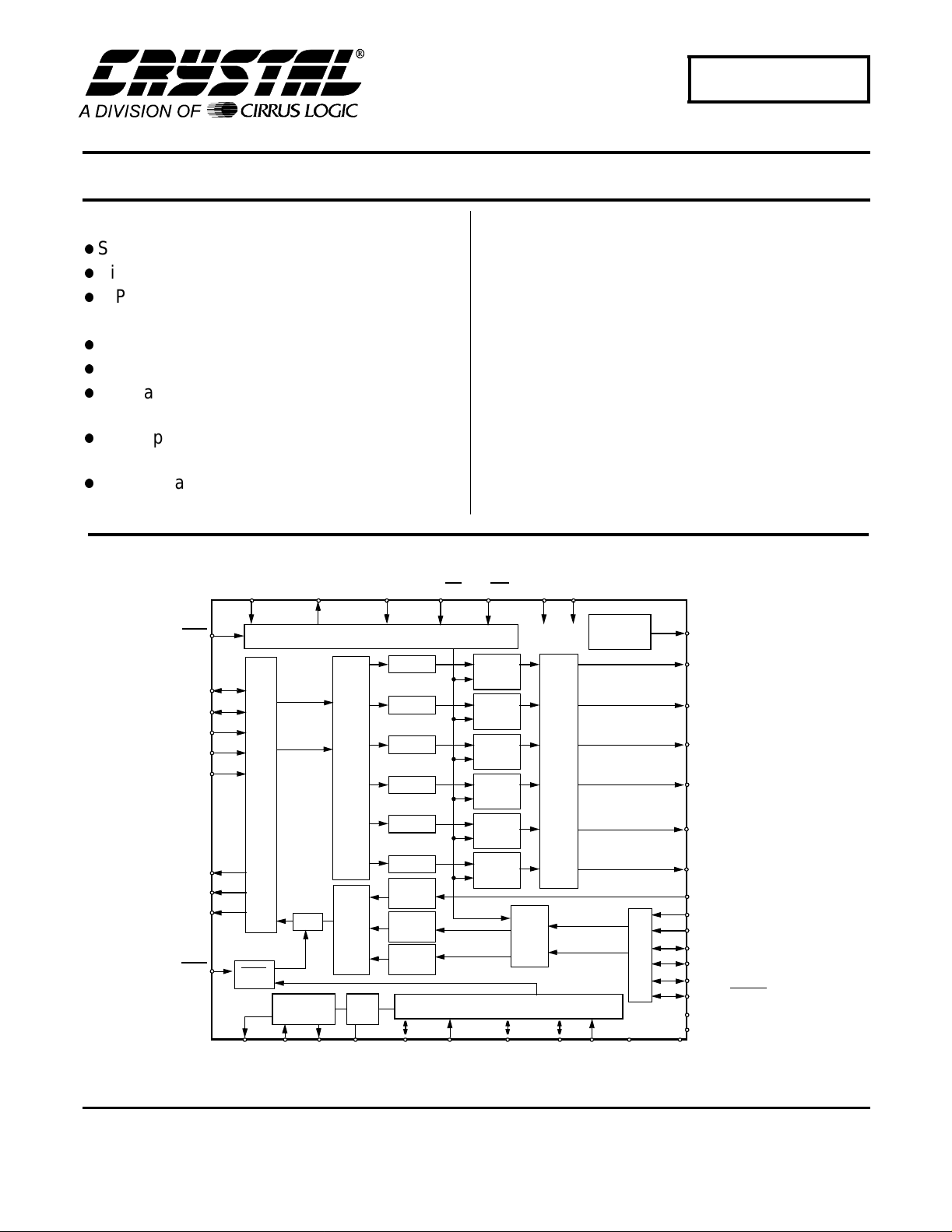
Serial Audio Data Interface
MUX
Clock Osc/
Divider
AD1/CDIN AD0/CS I2C/SPI
Control Port
DAC#1
DAC#2
DAC#3
DAC#4
Digital Filters
DAC#5 Volume
DAC#6
Mono
ADC
Left
ADC
Right
Digital Filters
ADC
PLL
FILT
HOLD/RUBIT
DATAUX/RX4
Description
The CS4226 is a single-chip codec providing stereo analog-to-digital and six digital-to-analog converters using
delta-sigma conversion techniques. This +5 V device
also contains volume control independently selectable
for each of the six D/A channels. An S/PDIF receiver is
included as a digital input channel. Applications include
Dolby Pro-logic, THX, DTS an d Dolby Digi tal AC-3 home
theater systems, DSP based car audio systems, and
other multi-channel applications.
The CS4226 is packaged in a 44-pin plastic TQFP.
ORDERING INFORMATION
CS4226-KQ -10° to +70° C 44-pin TQFP
CS4226-BQ -40° to +85° C 44-pin TQFP
CDB4226 Evaluation Board
VD+
VA+
Volume
Control
Volume
Control
Volume
Control
Volume
Control
Analog Low Pass and
Control
Volume
Control
Input
Gain
S/PDIF RX/Auxiliary Input
LRCKAUX/RX3
SCLKAUX/RX2
Output Stage
RX1
Voltage
Reference
Input MUX
DGND1
CMOUT
AOUT1
AOUT2
AOUT3
AOUT4
AOUT5
AOUT6
AINAUX
AIN1L
AIN1R
AIN2L/FREQ 0
AIN2R/FR EQ 1
AIN3L/AUTODATA
AIN3R/AUDIO
AGND1
AGND2
DGND2
Cirrus Logic, Inc.
Crystal Semiconductor Products Division
P.O. Box 17847, Austin, Texas 78760
(512) 445 7222 FAX: (512) 445 7581
http://www.crystal.com
Copyright Cirrus Logic, Inc. 1998
(All Rights Reserved)
SEP ‘98
DS188F1
1
Page 2

TABLE OF CONTENTS
CHARACTERISTICS/SPECIFICATIONS ............................................................ 3
ANALOG C H A RA C T E RISTICS... .. .................... .............................. ............ 3
SWITCHING CHARACTERISTICS ............................................................. 5
SWITCHING CHARACTERISTICS - CONTROL PORT ............................. 6
S/PDIF RECEIVER CHARACTERISTICS................................................... 7
ABSOLUTE MAXIMUM RATINGS ........................................ ......................8
RECOMMENDED OPERATING CONDITIONS.......................................... 8
DIGITAL CHARACTERISTICS.................................................................... 8
FUNCTIONAL DESCRIPTION ..........................................................................10
Overview ......... ......... ....... ......... ......... .......... ...... .......... ......... ....... ......... ..... 10
Analog Inputs ............................................................................................ 10
Line Level Inputs ................................................................................ 10
Adjustable Input Gain ................ ................................................. ........11
High Pass Filter ..................................................................................11
Analog Outputs .........................................................................................11
Line Level Outputs .............................................................................11
Output Level Attenuator .....................................................................11
Clock Generation ......................................................................................12
Clock Source ......................................................................................12
Master Clock Output .......................................................................... 13
Synchron izat ion .... .. .... ..... .. ..... .... ..... .. ..... .... ... .... ..... ..... .. .... ..... ..... .. .... . 13
Digital Interfaces .......................................................................................13
Audio DSP Serial Interface Signals ..... .. .............................. ...............13
Audio DSP Serial Interface Formats ..................................................13
Auxiliary Audio Port Signals ...............................................................15
Auxiliary Audio Port Formats .............................................................. 15
S/PDIF Receiver ................................................................................15
AC-3/MPEG Auto Detection ............................................................... 16
Control Port Signals ..................................................................................16
SPI Mode ...........................................................................................16
2
C Mode ............................................................................................ 17
I
Control Port Bit Definitions .................................................................17
Power-up/Reset/Power Down Mode .........................................................18
DAC Calibration ........................................................................................18
De-Emphasis ............................................................................................ 18
HOLD Function ......................................................................................... 19
Power Supply, Layout, and Grounding .....................................................19
ADC and DAC Filter Response Plots .............................. ................... ......19
REGISTER DESCRIPTION ............................................................................... 21
PIN DESCR I P T IO N .................... .............................. ....................................... ...29
PARAMETER DEFINITIONS .............................................................................34
PACKAGE DIMENSIONS ..................................................................................35
CS4226
Advanced product information describes products which are in development and subject to development changes. Cirrus Logic, Inc. has made best
efforts to e nsur e tha t th e inf orma tion con tain ed i n th is doc ument is accur ate a nd r eliab le . How ever , th e inf orma tion is su bj ect to change without
notice a nd is p rov i ded “A S I S” w it ho ut wa rr an ty of an y ki n d (e x pre s s or i mpl i ed ). No r esp on s ibi l i ty is assume d by Cirrus L ogi c, In c . fo r t he us e of
this inf or ma ti on , n or f or i n f ring eme nt s of pa te nt s or o th er r i ght s o f t hi r d pa rt ies . Thi s doc u men t i s th e propert y of Cir r u s Lo gic , I nc. an d i mp li es no
license under patents, copyrights, trademarks, or trade secrets. No part of this publication may be copied, reproduced, stored in a retrieval system,
or trans mit te d, in any f orm or b y any me ans ( e lectronic , me c han ica l , pho to gra ph i c, or ot he rwi s e). Fur th er mo r e, no pa rt of this publi cat i o n may be
used as a basis for manufacture or sale of any items without the prior writte n consent of Cirrus Logic, Inc. The names of products of Cirrus Logic,
Inc. or other vendors and suppliers appearing in this document may be trademarks or service marks of their respective owners which may be registered in some jurisdictions. A list of Cirrus Logic, Inc. trademarks and service marks can be found at http://www.cirrus.com.
Dolby and AC-3 are registered trademarks, Dolby Pro-Logic is a trademark of Dolby Laboratories Licensing Corporation. DTS is a registered trademark of DTS, Inc.. THX is a registered trademark of LucasArts Entertainment Company. I
2
C is a registered trademark of Philips Semiconductor.
2 DS188F1
Page 3

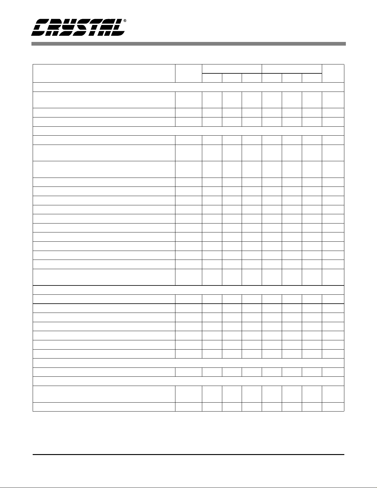
CHARACTERISTICS/SPECIFICATIONS
CS4226
ANALOG CHARACTERISTICS (T
990.52 Hz; Fs = 44.1 kHz (PLL in use); Measurement Bandwidth is 20 Hz to 20 kHz; Local components as shown
in Figure 1; SPI mode, Format 3, unless otherwise specified.)
Parameter Symbol
Analog Input Characteristics
ADC Resolution Ste reo Audio channels
Total Harm onic Dis tortion THD 0.003 - 0.003 - %
Dynamic Range (A weighted, Ster eo)
Total Harmonic -1 dB, Stereo (Note 1)
Distortion + Noise -1 dB, Mono (Note 1)
Interchannel Isolation - 90 - - 90 - dB
Interchannel Gain Mismatch - 0.1 - - 0.1 - dB
Programmable Input Gain Span 8 9 10 8 9 10 dB
Gain Step Size 2.7 3 3.3 2.7 3 3.3 dB
Offset Error (wi th high pass filter) - - 0 - - 0 LSB
Full Scale Input Voltage (Single Ended): 0.90 1.0 1.10 0.90 1.0 1.10 Vrms
Gain Drift - 100 - - 100 -
Input Resistance (Note 2) 10 - - 10 - - k
Input Capacitance - - 15 - - 15 pF
CMOUT Output Voltage - 2.3 - - 2.3 - V
- Minimum gain setting (0 dB) Differ ential Input; unless otherwise specified.
Mono channel
(unweighted, Stereo)
(A weighted, Mono)
= 25°C; VA+, VD+ = +5V; Full Scale Input Sine wave,
A
CS4226-KQ CS4226-BQ
16
16
92
-
89
THD+N -
-
-
20
-
20
95
92
-
-88--82
-
-
-
-72
16
16
90
87
-
-
-
-
20
-
20
93
90
-
-86--80
-
-
-
-70
UnitsMin Typ Max Min Typ Max
Bits
Bits
dB
dB
dB
dB
dB
ppm/°C
Ω
A/D Decimation Filter Characteristics
Passband (Note 3) 0.02 - 20.0 0.02 - 20.0 kHz
Passband Ripple - - 0.01 - - 0.01 dB
Stop band (Note 3) 27.56 Stop band Attenuation (Note 4) 80 - - 80 - - dB
Group Delay (Fs = Output Sam ple R a te)
Group Delay Variation vs. Frequenc y
(Note 5) t
gd
∆
t
gd
- 15/Fs - - 15/Fs - s
--0--0µs
5617.2
27.56 -
5617.2
kHz
Notes: 1. Referenced to typical full-scale differential input voltage (2Vr ms).
2. Input resistance is for the input selected. Non-selected inputs have a very high (>1MΩ) input resi stance.
The input resistance will vary with gain value selected, but will always be greater than the min. value
specified
3. Filter characteristics scale with output sample rate.
4. The analog modulator samples the input at 5.6448 MHz for an out put sample rate of 44. 1 kHz. There is
no rejection of input signal s which are multiple s of the sampling frequen cy (n × 5.6448 MHz ± 20.0 kHz
where n = 0,1,2,3...).
5. Group delay for Fs = 44.1 kHz, t
DS188F1 3
= 15/44.1 kHz = 340 µs
gd
Page 4
CS4226
ANALOG CHARACTERISTICS (Continued)
CS4226-KQ CS4226-BQ
Parameter Symbol
High Pass Filter Characteristics
Frequency Response: -3 dB (Note 3)
-0.13 dB
Phase Deviation @ 20 Hz (Note 3) - 10 - - 10 - Deg.
Passband Ripple - - 0 - - 0 dB
Analog Output Characteristics
DAC Resolution 16 - 20 16 - 20 Bits
Signal-to-N oi se/Idle (DAC m ut ed, A weighted)
Channel Noise
Dynamic Range (DAC not muted, A weighted)
(DAC not muted, unweighted)
Total Harmonic Distortion THD - 0.003 - - 0.003 - %
Total Harmonic Distortion + Noise (Stereo) THD+N - -88 -83 - -86 -81 dB
Interchannel Isolation - 90 - - 90 - dB
Interchannel Gain Mismatch - 0.1 - - 0.1 - dB
Attenuation Step Size (All Output s) 0.7 1 1.3 0.7 1 1.3 dB
Programmable Output Attenuation Span -84 -86 - -84 -86 - dB
Offset Voltage (relative to CMOUT) - ±15 - - ±15 - mV
Full Scale Output Voltage 0.92 1.0 1.08 0.92 1.0 1.08 Vrms
Gain Drift - 100 - - 10 0 -
Out-of-Band Energy (Fs/2 to 2Fs) - -60 - - -60 - dBFs
Analog Output Load Resistance:
- Minimum Attenuation, 10 k, 100 pF load; unless otherwise specified.
Capacitance:
-
3.4
-
20
101 108 - 99 106 - dB
93
10
98
-
95
-
-
-
-
-
-
-
-
100
91
10
-
3.4
-
20
96
-
93
-
-
-
100
Combined Digital and Analog Filter Characteristics
Frequency Response 10 Hz to 20 kHz - ±0.1 - - ±0.1 - dB
Deviation from Linear Phase - ±0.5 - - ±0 .5 - Deg.
Passband: to 0.01 dB corner (Notes 6, 7) 0 - 20.0 0 - 20.0 kHz
Passband Ripple (Note 7) - - ±0.01 - - ±0.01 dB
Stopband (Notes 6 ,7) 24.1 - - 24.1 - - kHz
Stop band Attenuation (Note 8) 70 - - 70 - - dB
Group Delay (Fs = Input Word Ra te) (Note 5) tgd - 16/Fs - - 16/Fs - s
Analog Loopback Performance
Signal-to-noise Ratio (CCIR-2 K w eig ht ed, -2 0 dB input) CCIR-2K
-71- -71-dB
Power Supply
Power Supply Current Operating
Power Down
Power Supply Rejection (1 kHz, 10 mV
Notes: 6. The passband and stopband edges scale wit h frequency. For input word ra tes, Fs, other than 44.1 kHz,
the 0.01 dB passband edge is 0.4535×Fs and the stopband edge is 0.5465×Fs.
7. Digital filter characteristics.
8. Measurement bandwidth is 10 Hz to 3 Fs.
) - 45 - - 45 - dB
rms
-
-
901113
3
-
9011153mA
-
-
-
-
-
-
UnitsMin Typ Max Min Typ Max
Hz
Hz
dB
dB
ppm/°C
Ω
k
pF
mA
4 DS188F1
Page 5
CS4226
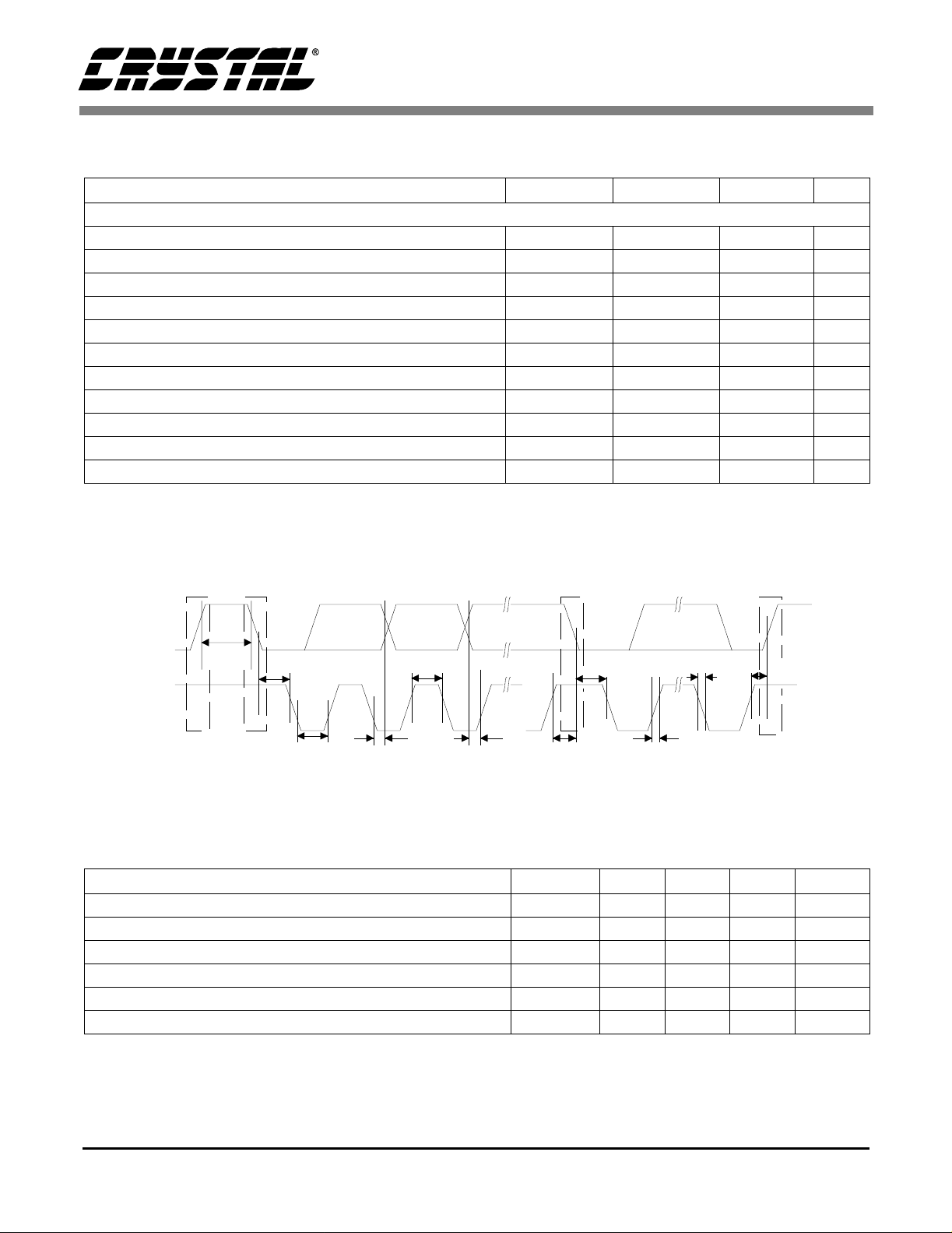
SWITCHING CHARACTERISTICS (T
= 25°C; VA+, VD+ = +5V ±5%, outputs loaded with 30 pF)
A
Parameter Symbol Min Typ Max Units
Audio ADC's & DAC's Sample Rate Fs 4 - 50 kHz
XTI Frequency (XTI = 256, 384, or 512 Fs) 1.024 - 26 MHz
XTI Pulse Width High XTI = 512 Fs
XTI = 384 Fs
XTI = 256 Fs
XTI Pulse Width Low XTI = 512 Fs
XTI = 384 Fs
XTI = 256 Fs
10
21
31
10
21
31
-
-
-
-
-
-
-
-
-
-
-
-
ns
ns
ns
ns
ns
ns
PLL Clock Recovery Frequency RX, XTI, LRCK, LRCKAUX 30 - 50 kHz
XTI Jitter Tolerance - 500 - ps
Low Time (Note 9) 500 - - ns
PDN
SCLK Falling Edge to SDOUT Output Valid (DSCK = 0) t
LRCK edge to MSB valid t
SDIN Setup Time Before SCLK Rising Edge (DSCK=0) t
SDIN Hold Time After SCLK Rising Edge (DSCK=0) t
dpd
lrpd
ds
dh
-- ns
--40ns
--25ns
--25ns
1
--------------------
384()Fs
20+
Master Mode
SCLK Period t
SCLK Falling to LRCK Edge (DSCK=0) t
sck
mslr
1
--------------------
256()Fs
--ns
-±10 - ns
SCLK Duty Cycle - 50 - %
Slave Mode
SCLK Period t
SCLK High Time t
SCLK Low Time t
SCLK Rising to LRCK Edge (DSCK=0) t
LRCK Edge to SCLK Rising (DSCK=0) t
sckw
sckh
sckl
lrckd
lrcks
1
--------------------
128()Fs
--ns
40 - - ns
40 - - ns
20 - - ns
40 - - ns
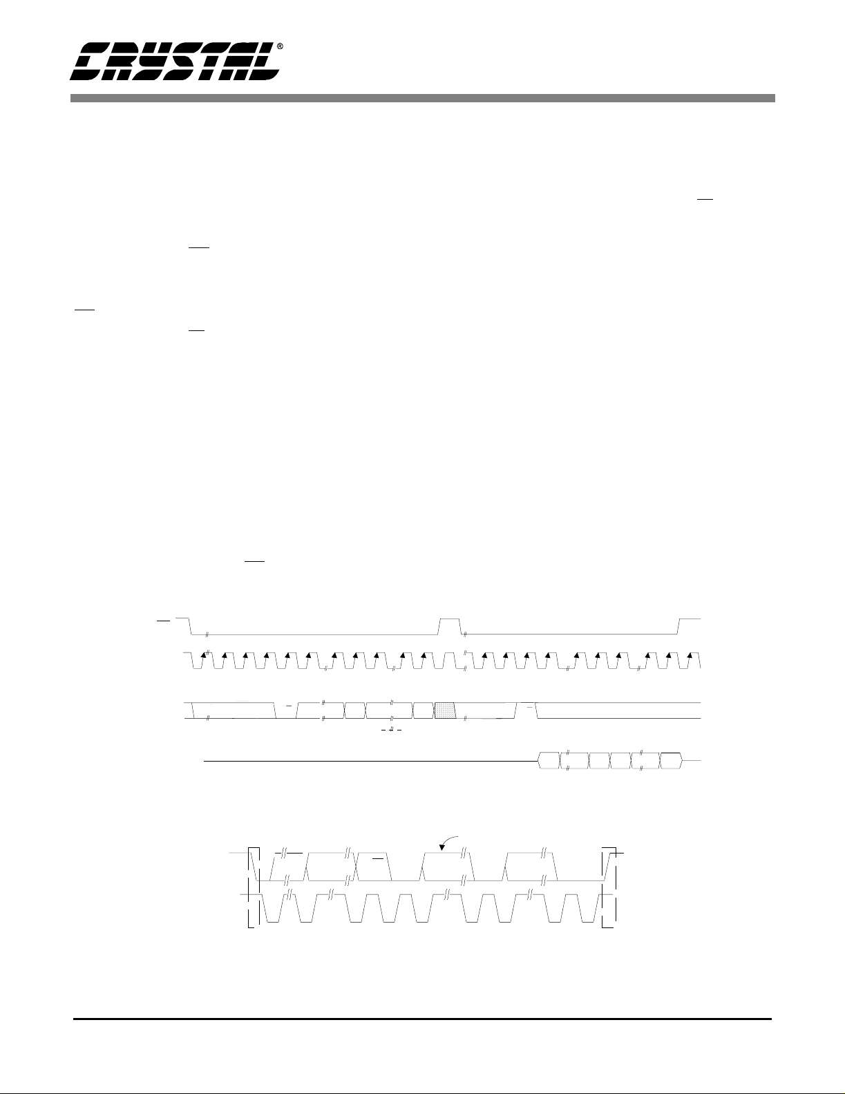
Notes: 9. After powering up the CS4226, PDN
SCLK*
SCLKAUX*
(output)
t
LRCK
LRCKAUX
(output)
SDOUT1
SDOUT2
Audio Ports Master Mode Timing
mslr
should be held low until the power supply is settled.
LRCK
LRCKAUX
t
sck
(input)
SCLK*
SCLKAUX*
(input)
SDIN1
SDIN2
SDIN3
DATAUX
SDOUT1
SDOUT2
*SCLK, SCLKAUX shown for DSCK = 0 and ASCK = 0.
SCLK & SCLKAUX inverted for DSCK = 1 and ASCK = 1, respectively.
t
lrckd
t
lrpd
t
lrcks
t
sckh
t
t
ds
dh
MSB
Audio Ports Slave Mode and Data I/O timing
t
sckw
t
sckl
t
dpd
MSB-1
DS188F1 5
Page 6
CS4226
SWITCHING CHARACTERISTICS - CONTROL PORT (TA = 25°C VD+, VA+ = 5V ±5%;
Inputs: logic 0 = DGND, logic 1 = VD+, CL = 30 pF)
Parameter Symbol Min Max Units
SPI Mode
CCLK Clock Frequency f
High Time Between Transmissions t
CS
Falling to CCLK Edge t
CS
CCLK Low Time t
CCLK High Time t
CDIN to CCLK Rising Setup Time t
CCLK Rising to DATA Hold Time (Note 10) t
CCLK Falling to CDOUT stable t
Rise Time of CDOUT t
Fall Time of CDOUT t
Rise Time of CCLK and CDIN (Note 11) t
Fall Time of CCLK and CDIN (Note 11) t
(SPI/I2C = 0)
sck
csh
css
scl
sch
dsu
dh
pd
r1
f1
r2
f2
-6MHz
1.0
µ
20 ns
66 ns
66 ns
40 ns
15 ns
45 ns
25 ns
25 ns
100 ns
100 ns
s
Notes: 10. Data must be held for sufficient time to bridge the transition time of CCLK.
11. For F
SCK
< 1 MHz
CS
CCLK
CDIN
CDOUT
t
css
t
r2
t
scl
t
t
f2
dsu
t
sch
t
dh
t
csh
t
pd
6 DS188F1
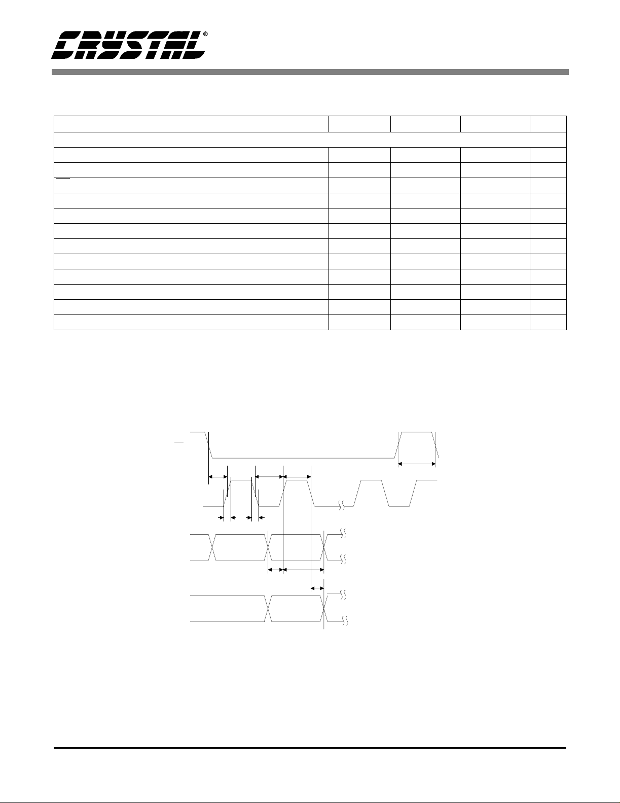
Page 7
CS4226
SWITCHING CHARACTERISTICS - CONTROL PORT (T
Inputs: logic 0 = DGND, logic 1 = VD+, CL = 30 pF)
Parameter Symbol Min Max Units
I2C® Mode
SCL Clock Frequency f
Bus Free Time Between Transmissions t
St art Condition Hold Time (prior to first cl ock pulse) t
Clock Low Time t
Clock High Time t
Setup Time for Repeated Start Condition t
SDA Hold Time from SCL Falling (Note 13) t
SDA Setup Time to SCL Rising t
Rise Time of Both SDA and SCL Lines t
Fall Time of Both SDA and SCL Lines t
Setup Time for Stop Condition t
Notes: 12. I
(SPI/I2C = 1) (Note 12)
scl
buf
hdst
low
high
sust
hdd
sud
r
f
susp
2
C is a registered trademark of Philips Semiconductors.
13. Data must be held for sufficient ti me to bridge the 300 ns transition time of SCL.
Repeated
Stop Start
Start
= 25°C; VD+, VA+ = 5V ±5%;
A
-100kHz
4.7
4.0
4.7
4.0
4.7
0
µ
s
µ
s
µ
s
µ
s
µ
s
µ
s
250 ns
1
µ
s
300 ns
4.7
Stop
µ
s
SDA
SCL
t
buf
t
hdst
t
low
t
hdd
t
high
t
sud
t
sust
t
hdst
t
f
t
r
t
susp
S/PDIF RECEIVER CHARACTERISTICS (RX1, RX2, RX3, RX4 pins onl y; VD+, VA+ = 5V ±5%)
Parameter Symbol Min Typ Max Units
Input Resistance Z
Input Voltage V
Input Hysteresis V
HYST
Input Sample Frequency F
N
TH
S
-10- k
200 - - mVpp
-50-mV
30 - 50 kHz
CLKOUT Jitter (Note 14) - 200 - ps RMS
CLKOUT Duty Cycle (high time/cycle time) (Note 15) 40 50 60 %
Notes: 14. CLKOUT Jitter is for 256×FS selected as output frequency measured from falling edge to falling edge.
Jitter is greate r for 384×Fs and 512×Fs as selected output fr equency.
15. For CLKOUT frequency equal to 1×Fs, 384×Fs, and 512×Fs. See Master Clock Output section.
Ω
DS188F1 7
Page 8
CS4226
ABSOLUTE MAXIMUM RATINGS (AGND, DGND = 0 V, all voltages with respect to 0 V.)
Parameter Symbol Min Typ Max Units
Power Supplies Digital
Analog
Input Current (Note 16) - - ±10 mA
Analog Input Voltage (Note 17) -0.7 - (VA+)+0.7 V
Digital Input Voltage (Note 17) -0.7 - (VD+)+0.7 V
Ambient Temperature (Power Applied) -55 - +125 °C
Storage Temperature -65 - +150 °C
Notes: 16. Any pin except supplies. Transient currents of up to ±100 mA on the analog input pins will not cause
SCR latch-up.
17. The maximum over or under voltage is limited by the i nput current.
Warning: Operation at or beyond these li mit s may result in permanent damage to the device. Normal operation
is not guaranteed at these extremes.
RECOMMENDED OPERATING CONDITIONS (AGND, DGND = 0 V, all voltages with r espect
to 0 V.)
VD+
VA+
-0.3
-0.3
-
-
6.0
6.0
V
V
Parameter Symbol Min Typ Max Units
Power Supplies Digital
|(VA+)-(VD+)|<0.4 V Analog
Operating Ambient Temperature CS4226-KQ
CS4226-BQ
DIGITAL CHARACTERISTICS (T
Parameter Symbol Min Typ Max Units
High-level Input Voltage (except RX1) V
Low-level Input Voltage (except RX1) V
High-level Output Voltage at I
Low-level Output Voltage at I
Input Leakage Current (Digital Inputs) - - 10
Output Leakage Current (Hi gh-Impedance Digital Outputs) - - 10
= -2.0 mA V
0
= 2.0 mA V
0
= 25 °C; VA+, VD+ = 5 V ±5%)
A
VD+
VA+
T
A
IH
IL
OH
OL
4.75
4.75
-10
-40
2.8 - (VD+)+0.3 V
-0.3 - 0.8 V
(VD+)-1.0 - - V
--0.4V
5.0
5.0
25
25
5.25
5.25
70
85
V
V
°C
°C
µ
A
µ
A
8 DS188F1
Page 9
CS4226
Ferrite Bead
+5V
Supply
To Optional
Input and
1
µ
Output Buffers
10 µF
10 µF
10 µF
10 µF
10 µF
From Optional Input Buffer
10
10 µF
R
S
R
S
R
S
Digital
Audio
Source
100 pF
R
S
100 pF
R
S
100 pF
R
S
100 pF
Mode
Setting
R = 50
Ω
S
R = 475
Ω
D
All unus ed digital in puts
should be tied to DGND.
All unus ed analog inputs
should be left floating.
* Optional if analog i nput s
biased to within 1% of
CMOUT
† Only needed when inputs
are used for S/PDIF.
F
µ
F
2.0
Ω
1 µF 0.1 µF
+
19
1 µF 0.1 µF
+
40
VA+ VD+
16
CMOUT
+
14
*
AIN1L
13
*
AIN1R
11
*
AIN2L/FREQ0
12
*
AIN2R/FREQ1
10
*
AIN3L/AUTODATA
9
*
AIN3R/AUDIO
15
*
AINAUX
27
DEM
2
HOLD/RUBIT
42
RX1
CS4226
†
1
DATAUX/RX4
†
44
LRCKAUX/RX3
†
43
SCLKAUX/RX2
SDA/CDOUT
†
8
PDN
7
2
I C/SPI
AGND1, 2 DGND1, 2 FILT XTO XTI
39412018
17
R
FILT
29 28
R **
X1
Loop Current
Normal High
C
15 nF
43 k
1.5 nF
Ω
180 nF
3.3 k
18 nF
FILT
R
FILT
C
RIP
C
FILT
Ω
C
RIP
Figure 1. Recommended Connection Diagram
AOUT1
AOUT2
AOUT3
AOUT4
AOUT5
AOUT6
SCL/CCLK
AD0/CS
AD1/CDIN
SDIN1
SDIN2
SDIN3
SDOUT1
SDOUT2
LRCK
SCLK
CLKOUT
OVL/ERR
R **
X2
C1** C2**
21
22
23
24
25
26
3
4
6
5
34
33
32
36
35
37
38
31
30
ANALOG
FILTER
ANALOG
FILTER
ANALOG
FILTER
ANALOG
FILTER
ANALOG
FILTER
ANALOG
FILTER
Microcontroller
R
D
R
D
R
D
R
S
R
S
R
S
R
S
**
C1
C2
R
R
Audio
DSP
1xFs
40 pF 40 pF
10 pF 40 pF
300 k
X1
X2
10 M
Ω
Ω
256,
384,
512xFs
short
open
DS188F1 9
Page 10
CS4226
FUNCTIONAL DESCRIPTION
Overview
The CS4226 has 2 channels of 20-bit analog-todigital conv ersion and 6 cha nnels of 20-bit d igi talto-analog con version. A mono 20-bit A DC is also
provided. All ADCs and DACs are delta-sigma
converters. The stereo ADC inputs have adjustable
input gai n, while th e DAC outputs have adjustab le
output attenuation. The device also contains an
S/PDIF rece iver capable o f receiving compre ssed
AC-3/MPEG or un compressed digita l audio data.
Digital audio data for the DACs and from the
ADCs is communicate d over separat e serial ports.
This allows concurrent writing to and reading from
the device. The CS4226 functions are controlled
via a serial microcontroller interface. Figure 1
shows the recommended connection diagram for
the CS4226.
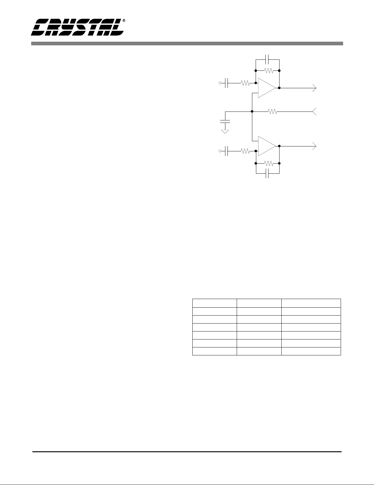
Analog Inputs
Line Level Inputs
AIN1R, AIN1L, AIN2R, AIN2L, AIN3 R, AIN3L
and AINAUX are the line level input pins (See Figure 1). These pins are internally biased to the
CMOUT volta ge. A 10 µF DC blocking ca pacitor
placed in se ries with the input pins allows sign als
centered around 0 V to be input to the CS4226. Figure 2 shows an opt ional dual op amp bu ffe r which
combines leve l shi fti ng wi th a g ain of 0. 5 to att en uate the stan dard line level of 2 V rms to 1 Vrms.
The CMOUT reference level is used to bias the opamps to approximately one half the supply voltage.
With this input circuit, the 10 µF DC blocking caps
in Figure 1 may be omitted. Any remaining DC offset will be remov ed by the inte rnal high-pass filters.
100 pF
Line In
Right
Example
Op-Amps are
MC34074 or
MC33 07 8
Line In
Left
3.3 µF
3.3 µF
Figure 2. Optional Line Input Buffer
20 k
0.47 µF
20 k
-
+
+
-
10 k
AINxR
5 k
CMOUT
AINxL
10 k
100 pF
ADC Control Byte. On-chip anti-aliasing filters
follow the input mux providing anti-aliasing for all
input chan nels.
The analog inputs may also be configured as differential inputs. This is enabled by setting bits
AIS1/0=3. In the differential configuration, the left
channel inputs reside on pins 10 and 11, and the
right channel inputs reside on pins 12 and 13 as described in Ta ble 1 belo w. In d iff erent ial mode , the
full scale input level is 2 Vrms.
Single-ended Pin # Differential Inputs
AIN3L Pin 10 AINL+
AIN3R Pin 9 unused
AIN2L Pin 11 AINLAIN2R Pin 12 AINRAIN1L Pin 14 unused
AIN1R Pin 13 AINR+
Table 1. Single-ended vs Differential Input Pin
Assignments
The analog signal is input to the mono ADC via the
AINAUX pin.
Selection of stereo the input pair (AIN1L/R,
AIN2L/R or AIN3 L/ R) for the 20-bit ADC’s is accomplished by setting the AIS1/0 bits (ADC analog
Independen t Muting of both the ste reo ADC’s and
the mono ADC is p ossible throu gh the ADC Control Byte with the MUTR, MUTL and MUTM bits.
input mux control), which are accessible in the
10 DS188F1
Page 11

CS4226
Adjustable Input Gain
The signals from the line inputs are routed to a programmable ga in circui t which provi des up to 9 dB
of gain in 3 dB steps. The gain is adjustable
through the Input Control Byte. Right and left
channel gai n settings ar e contro lled indepe ndently
with the GNR1/0 and GNL1 /0 bits. Level cha nges
occur immediately on register updates. To minimize audible artifacts, level changes should be
done with the cha nne l muted.
The ADC Status Report Byte provides feedback of
input level for each ADC channel. This register
continously monitor s the ADC o utput and rec ords
the peak output level since the last register read.
Reading this register causes it to reset to 0 and peak
monitorin g begins again.
High Pass Filter
The operational amplifiers in the input circuitry
driving the CS4226 may generate a small DC offset
into the A/D converter. The CS4226 includes a
high pass filter af ter the decimator to remove any
DC offset which could result in recording a DC level, possibly yielding "clicks" when switching between dev ices in a multichannel system.
The characte ristics of this first- order high pa ss filter are outlined Table 2 below for an output sample
rate of 44.1 kHz. This filter response scales linearly
with sample rate.
Frequency Response -3dB @ 3.4 Hz
-0.13 dB @ 20 Hz
Phase Deviation 10 degrees @ 20 Hz
Passband Ripple None
Table 2. High Pass Filter Characteristics
Analog Outputs
Line Level Outputs
The CS42 26 contains an on-chip buffer amplifier
producing sing le-ende d outputs ca pable of drivin g
10 kΩ loads. Each output (A
1-6) will produce
OUT
a nominal 2.83 Vpp (1 Vrms) output with a 2.3 volt
quiescent v olta ge for a ful l scal e dig ital inpu t. The
recommende d off-chip ana log filter is a 2nd order
Butterworth with a -3 dB corner at Fs, see Figure 3.
This filter provides out-of-band noise attenuation
along with a gain of 2, providing a 2 Vrms output
signal. A 3rd order B utterworth filt er with a -3dB
corner at 0.75 Fs can be used if greater out of band
noise filtering i s desired. The C S4226 DAC int erpolation filter is a linear phase design which has
been pre-compensated for an external 2nd order
Butterworth filter to provide a flat frequency response and linear phase response over the passband. If this filter is not used, small frequency
response magnit ude and phase er rors wi ll occ ur.
Output Level Attenuator
The DAC outputs are each routed through an attenuator which is ad just able in 1 dB steps. Outp ut attenuation is available through the Output
Attenuator Data Bytes. Level changes are implemented in the analog domain such that the noise is
attenuat ed by the sa me a mo unt as the s ignal , until
the residual outpu t noise is equ al to the noise floo r
in the mu te st ate; at t his point atten ation is imple mented in the digital domain. The change from analog to dig ital at te nuat io n occu rs at -23 dB. Lev el
changes only take effect on zero crossings to minimize audible artifac ts. If th ere is no zero crossi ng,
then the requested level change will o ccur after a
time-out period between 512 and 1024 frames
(11.6 ms to 23.2 ms at 44. 1 kHz frame rate). Ther e
is a separate ze ro crossing det ector for ea ch channel. Each ACC bit (Acceptance bit) in the DAC
Status Report B yte give s feedba ck on w hen a vol ume control cha nge h as ta ken e ffect . T his bit goes
high when a new setting i s loaded and ret urns low
when it has taken eff ect. Volume control cha nges
can be instanta neous by setting the Ze ro Crossing
Disable (ZCD) bit in th e DAC Control Byte to 1.
Each outp ut can b e ind epend ently m uted via mu te
control bits, MUT6-1, in the DAC Control Byte.
DS188F1 11
Page 12

CS4226
The mute also takes effect on a zero-crossing or after a timeout. In add ition, the CS4226 has an optional mute on conse cu t ive zeros f eature, whe r e all
DAC outputs wi ll mu te if they re ceive betwe en 512
and 1024 conse cutive z eros (or - 1 cod e) on all six
channels. A sing le no n-zer o v alue will unm ute t he
DAC outputs. This feature can be disabled with the
MUTC bit in the DAC Con trol Byte. When using
the internal PLL as the clock source, all DACs will
instantly mute when the PLL detects an error.
Clock Generation
The master clock to operate the CS4226 may be
generated by using t he on -ch ip in verte r a nd an ex -
150pF
22 k
Ω
A
A
OUT
OUT
11 k
C
MOUT
1.1 k
5600 pF
C
MOUT
Ω
3.9 k
Ω
2-Pole Butterworth Filter
4.75 k
Ω
1000pF
5 k
Ω
Ω
5.85 k
1.21 k
5600 pF
5 k
_
+
0.47 µF
560 pF
Ω
Ω
_
+
Ω
0.47 µF
Example
Op-Amps
are
MC33078
ternal crys tal, by usin g the o n-chip PL L, or by u sing an external clock source. In all modes it is
required to ha ve SCL K a nd LRCK synchrono us t o
the selected master clock.
Clock Source
The CS4226 requires a high frequency master
clock to run th e internal logic. The Clock Source
bits, CS0/1/2 in Clo ck Mode Byte, determine the
source of the clock. A high frequency crystal can be
connected to XTI and XTO, or a high frequency
clock can be applied to XTI. In both these cases, the
internal PLL is disabled, and the VCO turns off.
The externa lly supplied high frequency cl ock can
be 256 Fs, 384 Fs or 512 Fs; this is set by the CI0/1
bits in the C lock Mode Byte. W hen using the on chip cry stal oscillat or, external loading capa citors
are required, see Figure 1. High frequency crystals
(>8MHz) should be pa ra ll el resonant, fun da mental
mode and designed for 20 pF loading (equivalent to
40 pF to grou nd on each leg).
Alternatively, the on-chip PLL may be used to generate the requi red high frequency cl ock. The PLL
input clock is 1 Fs, and may be input from LRCKAUX, LRCK, or from XTI/XTO. In this last case,
a 1 Fs clock may be input into XTI, or a 1 Fs crystal
attache d across XTI/XTO . When an exte rnal 1 Fs
crystal is attached, extra components will be required, see Figure 1. The PLL will lock onto a new
1 Fs clock in about 90 ms. If the PLL input clock is
removed, the VCO will drif t to the low f requency
end of its freque nc y range.
The PLL can also be used to lock to an S/PDIF data
source on RX1, R X2, R X3, or RX4. So urce se lection is ac complished with the CS2/1/0 bits in the
Clock Mode Byte. The PLL will lock to an S/PDIF
source in about 90 ms.
Finally, the PLL has two filter loop current modes,
3-Pole Butterworth Filter
normal an d high current, th at are selecte d via the
LC bit in the Converter Control Byte. In the normal
Figure 3.
12 DS188F1
mode, the loop current is 25
µA. In the high current
Page 13

CS4226
mode, the loop current is 300 µA. The high current
mode allows the use of lower impedance filter
components which minimizes the influences of
board contamin ation. See th e table in Figur e 1 for
filter component values in each mode.
Master Clock Output
CLKOUT is a master clock output prov ided to allow synchronization of external components.
Available CLKOUT frequencies of 1 Fs, 256 Fs,
384 Fs, and 512 Fs, are selectable by the CO0/1
bits of the Clock Mode Byte.
Generation of CLKOUT for 384 Fs a nd 512 Fs is
accomplished wi th an on chi p c lock mult iplier and
may conta in clock j itter. Th e source o f the 25 6 Fs
CLKOUT is the output of the PLL or a divided
down clock from the XT I/XTO input. If 384 Fs is
chosen as the input clock at XTI and 256 Fs is chosen as the output, CLKOUT will have approximately a 33% duty cycle. In all other cases
CLKOUT will typically have a 50% duty cycle.
Synchronization
The DSP port and Auxiliary port must operate synchronously to the CS4 226 clo ck so urce. The serial
port will force a reset of the data paths in an attempt
to resynchroni ze if non-synchron ous data is in put
to the CS 4226. It is advisable to mute the DAC s
when changing from one clock source to another to
avoid the output of undesirable audio signals as the
CS4226 resynchronizes.
Digital Interfaces
There are 3 di gita l audio int erfac e ports: the au dio
DSP port, the auxiliary digital audio port, and the
S/PDIF reciever. The serial data is represented in
2’s complement format with the MSB-first in all
formats.
Audio DSP Serial Interface Signals
The serial interface clock, SCLK, is used for transmitting and receiving a udio data. T he active e dge
of SCLK is chosen by setting the DSCK bit in the
DSP Port Mode Byte. SCLK can be generated by
the CS422 6 (maste r mode) o r it ca n be inpu t from
an external SCLK source (slave mode). Mode selection is set with the DMS1/0 bits in the DSP Port
Mode Byte. The number of SCLK cycles in one
system sample period is programmable to be 32,
48, 64, or 128 by setting the DCK1/0 bits in the
DSP Port Mode Byte.
The Left/Right clock (LRCK) is used to indicate
left and right data and the start of a new sample period. It may be ou tput f rom the C S4226, or it may
be generated from an exte rnal controller. T he frequency of LRCK must be equal to the system sample rate, Fs.
SDIN1, SDIN2, and SDIN3 are the data input pins,
each of which drive a pair of DACs. SDOUT1 and
SDOUT2 can carry the output data from the two
20-bit ADC’s, the mono ADC, the auxili ary digital
audio port, and the S/PDIF receiver . Selectio n depends on the IS1/0 bits in the ADC control byt e.
The audio DSP port may also be configured so that
all 6 DAC’s data is input on SDIN1, and all 3
ADC’s data is output on SDOUT1. Table 3 outli nes
the serial in te rface ports.
DAC Inputs
SDIN1 left channel
right channel
single line
SDIN2 left channel
right channel
SDIN3 left channel
right channel
Table 3. DSP Serial Interface Ports
DAC #1
DAC #2
All 6 DAC channels
DAC #3
DAC #4
DAC #5
DAC #6
Audio DSP Serial Interface Formats
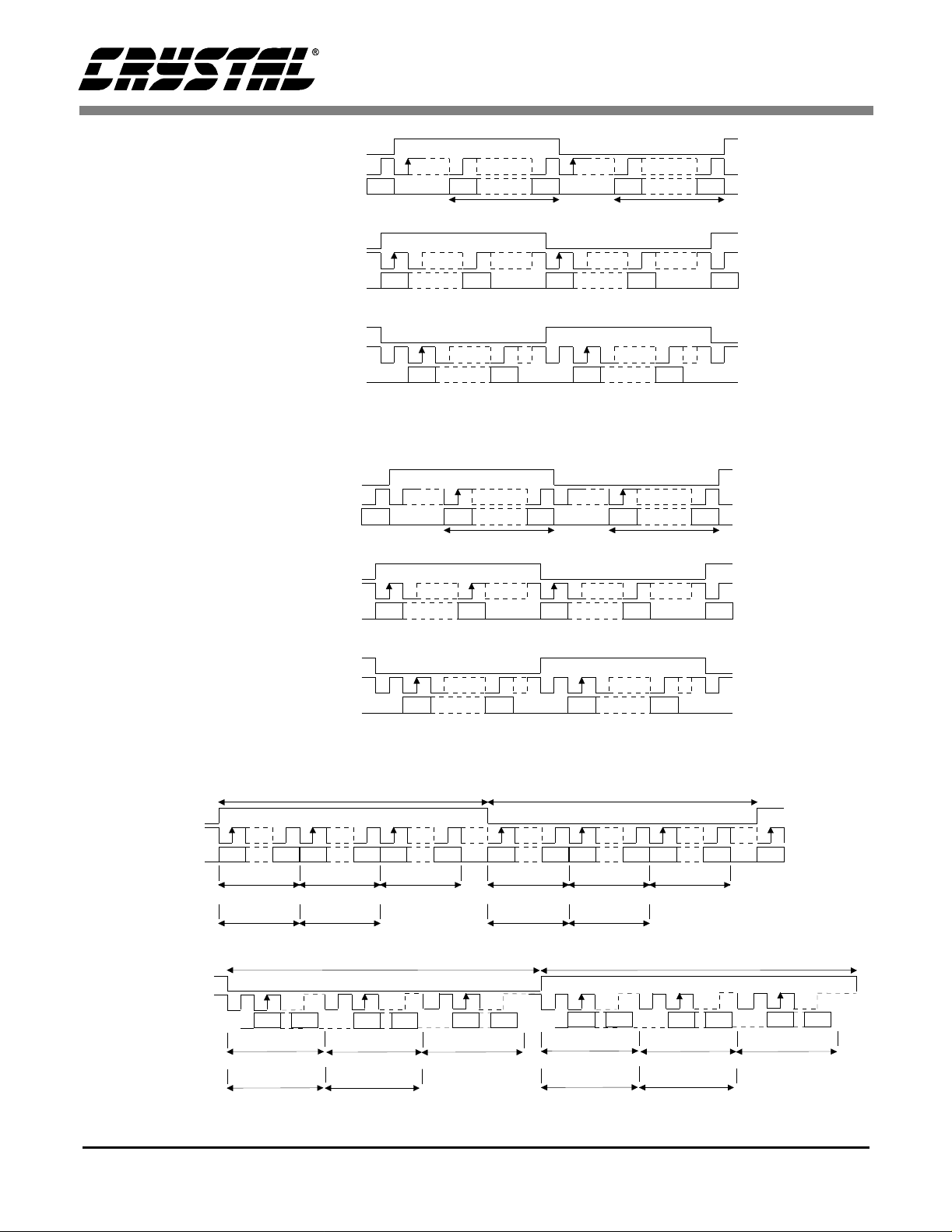
The audio DSP port supp orts 7 alternate formats,
shown in Figures 4, 5, and 6. These formats are
chosen through the DSP Port Mo de Byte with the
DDF2/1/0 bits.
Formats 5 and 6 a re single lin e data modes wh ere
all DAC chann els are co mbin ed onto a sin gle inpu t
DS188F1 13
Page 14
CS4226
FORMAT 0, 1, 2:
Format 0: M = 20
Format 1: M = 18
Format 2: M = 16
FORMAT 3:
FORMAT 4:
Note: SCLK shown for DSCK = 0. SCLK inverted for DSCK = 1.
Figure 4. Audio DSP and Auxiliary Port Data Input Formats
FORMAT 0, 1, 2:
Format 0: M = 20
Format 1: M = 18
Format 2: M = 16
FORMAT 3:
LRCK
SCLK
SDIN
LRCK
SCLK
SDIN MSB LSB
LRCK
SCLK
SDIN
LRCK
SCLK
SDOUT
LRCK
SCLK
SDOUT MS B LSB
LSB LSBMSB LSBMSB
MSB LS B
LSB LSBMSB LSBMSB
Left Right
Left Right
Left Right
Left Right
Left Right
M SCLKs
M SCLKs
M SCLKs
MSB LSB MSB
MSB LS B
M SCLKs
MSB LSB MSB
FORMAT 5:
FORMAT 6:
(MASTER
MODE
ONLY)
LRCK
SCLK
SDIN1
SDOUT1
LRCK
SCLK
SDIN1
SDOUT1
FORMAT 4:
Note: SCLK shown for DSCK = 0. SCLK inverted for DSCK = 1.
LRCK
SCLK
SDOUT
Left Right
MSB LS B
Figure 5. Audio DSP Port Data Output Formats
64 SCLKS 64 SCLKS
LSBMSB
DAC #1 DAC #3 DAC #5 DAC #2 DAC #4 DAC #6
20 clks
SDOUT1 SDOUT2 SDOUT1 SDOUT2
20 clks
(out)
(out)
LSBMSB
DAC #1
32 clks
SDOUT1
32 clks
LSBMSB LSBMSB LSBMSB LSBMSB LSBMSB MSB
20 clks
20 clks
128 SCLKS 128 SCLKS
32 clks
20 clks 20 clks
LSBMSB
DAC #3
SDOUT2
32 clks
20 clks
LSBMSB
DAC #5
32 clks
Figure 6. One data line modes
MSB LS B
20 clks 20 clks
20 clks
LSBMSB
DAC #2
32 clks
SDOUT1
32 clks
DAC #4
32 clks
SDOUT2
32 clks
LSBMSB
LSBMSB
DAC #6
32 clks
14 DS188F1
Page 15

CS4226
and all ADC ch annels are com bined onto a s ingle
output. Format 6 is available in Master Mode only.
See figure 6 for details.
Auxiliary Audio Port Signals
The auxil iary port pr ovide s an alt ernat e way to in put digital audio sig nals into the CS4226, and allows the CS4226 to syn chronize the system to an
external d igital audio source. This po rt consists of
serial clock , data and left /right clock pins named,
SCLKAUX, DATAUX and LRCKAUX. The
Auxiliary Audio Port inpu t is output on SDOUT1
when the IS bits are set to 1 or 2 in the ADC Control
Byte. Additionally, setting IS to 2 routes the stereo
ADC outputs to SDOUT2. There is approximately
a two frame delay from DATAUX to SDOUT1.
When the auxiliary port is used, the frequency of
LRCKAUX must equal to the system sample rate,
Fs, but no particular pha se relationship is required.
De-emphasis and muting on error conditions can be
performed on input data to the auxiliary audio port;
this is controlled by the Auxiliary Port Control
Byte.
Auxiliary Audio Port Formats
Data input on DATAUX is clocked into the part by
SCLKAUX using the format selected in the Auxiliary Port Mode Byte. The auxiliary audio port supports the same 5 formats as the audio DSP port in
multi-data line mode. LRCKAUX is used to indicate left and right data samp les, and t he start o f a
new sample period. SCLKAUX and LRCKAUX
may be output fro m the CS4226, or they may be
generated from an external source, as set by the
AMS1/0 control bits in the Auxiliary Port Mode
Byte.
S/PDIF Receiver
The CS4226 reconfigures its auxiliary digital audio
port as an S/PD IF rece iver if CS 2/1/ 0 in the Clock
Mode Byte ar e set to be 4, 5 , 6, or 7. In this mode
RX1, RX2, RX3, or RX4 can be chosen as the
S/PDIF input source.
The PLL will lock to the requested data source and
setting IS1/0 = 1 or 2 in the ADC Control Byte
routes the recovered output to SDOUT1 (channel A
to left, channel B to right). All 24 received data bits
will pass through the part to SDOUT1 except when
the serial port is configured with 32 SCLK’s per
frame or in Fo rmat 5. For these cases, the 16 or 20
MSB’s respectively will be output.
The error fl ags ar e repo rted i n the Re ceiv er St atus
Byte. The LOCK bit in dicate s whether th e PLL is
locked to the incoming S/PDIF data. Parity, Biphase, or Validity er rors (PAR=1, BIP=1 or V=1)
will cause the last valid data sample to be held at
the receiver input until the error condition no longer is pres ent (see H old se ctio n). Mu te o n e xt ende d
hold can also be enabled through the Auxiliary Port
Control Byte (see Hold section).
Other error flags include confidenc e, CONF, and
cyclic redundancy check, CRC. The CONF flag occurs when the received data eye opening is less
than half a bit period. This indicates that the quality
of the tra nsmission link i s poor and does not me et
the digital audio interface standards. The CRC flag
is updated at the beginning of a channel status
block and is onl y valid when the profe ssional format of chan nel status dat a is received. This error
indicates whe n the CS4226 calculate d CRC value
does not match the CRC byte of the received channel status block.
The OVL/ERR pin will go hi gh t o fla g an err or. It
is a latched logical OR of the Parity , Biphas e, Validity, and Lock error fla gs in the Recei ver Status
Byte which is reset at the end of each frame. However, Parity, Biphase, or Validity errors can be
masked from the pi n by cle aring the PM, BM, and
VM bits respectively, of the Input Control Byte.
The first four bytes of the Channel Status block for
both channel A and B can be acce ssed in the Receiver C hannel Status Bytes. When the CV bit is
DS188F1 15
Page 16
CS4226
high, these b ytes are bein g updated and may be invalid. Additionally, the audio/non-audio, AC3/MPEG data stream indicator and sampling frequency channel status bits may be output to pins 9,
10, 11 and 12, respectively, see Table 4. This is accomplish ed by setti ng th e CSP bi t to 1 in th e Aux iliary Status Output Byte. The FREQ0/1 channel
status bit outputs are decoded from the sampling
frequency channel status bits after first referencing
channel status byt e 0, bit 0 (PRO or consume r bit)
which indicates the appropriate location of these
bits in the channel status data stream.
The recei ved user bi t is outp ut on the HOLD/R UBIT pin if the HPC bit in the AUX Port Control
Byte is set to 1. It can be sampled with the rising or
falling edge of L RCK if the audio DSP port is in
Master Mode.
AUDIO Pin 9 0 - Audio data
1 - Non-audio data
AUTODATA Pin 10 0 - No preamble detected in
last 4096 frames
1 - Preamble detected
FREQ0/1 Pin 11/12 00 - 44.1 k Hz
01 - 48 kHz
10 - Reserved
11 - 32 kHz
Table 4. S/PDIF Receiver Status Outputs
is detected, the AUTODATA indicator (pin 10)
will go high. If no additional sync codes are detected within the next 4096 frames, the AUTODATA
indicator pin will return low until another sync
code is detected.
Control Port Signals
The control port is us ed to load all the internal settings. The operation of the control port may be
completely asynchronous with the audio sample
rate. However, to avoid potential interference
problems, the control port pins should remain static
if no operation is required.
The control port has 2 modes: SPI and I
2
C, with the
CS4226 as a slave device. The SPI mode is selected
by setting the I
by setting the I
2
C/SPI pin low, and I2C is se le cte d
2
C/SPI pin high. The state of this
pin is continuously monitored .
SPI Mode
In SPI mode, C S is the CS4 226 chi p sele ct sig nal,
CCLK is the c ontrol port bit cl ock, ( input into t he
CS4226 from the microcontroller), CDIN is the input data line from the mic rocontroll er, CDOUT is
the output dat a li ne to t he mi croco ntr oll er, an d the
chip address i s 00 10000. Dat a is c lock ed i n on t he
rising edge of CCLK and out on the falling edge.
AC-3/MPEG Auto Detection
For AC-3/MPEG applications, it is important to
know whether the incomi ng S/PDIF data strea m i s
digital audio or compressed AC-3/MPEG data.
This informati on is typically conveyed by settin g
channel status bit 1 (audio/non-audio bit), but some
AC-3/MPEG sources may not strictly adhere to this
convention and the bit may not be properly set. The
CS4226 S/PDIF receiver has the capability to automatically detect whether the incoming data is a
compressed AC-3/MPEG input. This is accomplished by looking for an AC-3 /MPEG 96-bit sync
code consisting of six 16-bit words. The 96-bit
sync code consists of: 0x0000, 0x0000, 0x0000,
0x0000, 0xF872, and 0x4E1F. When the sync code
16 DS188F1
Figure 7 shows the control port timing in SPI mode.
To write to a register, bring CS
low. The first 7 bits
on CDIN form the ch ip address, and they must be
0010000. The eighth bit is a read/write indicator
), which sho uld be low to write. The next 8
(R/W
bits form the Memory Address Pointer (MAP),
which is set to the address of the register that is to
be updated. T h e next 8 bits a re the data whi ch will
be placed into register designated by the MAP.
During writes, the CDOUT output stays in the high
impedance state. It may be externally pul led high
or low with a 47 k
Ω resistor.
The CS4226 has a MAP auto increment capability,
enabled by the INCR bit in the MAP register. If
INCR is a zero, then the MAP will stay constant for
Page 17
CS4226
successive reads or writes. If INCR is set to a 1,
then MAP will auto increment after each byte is
read or written, allowing bloc k reads or writes of
successive registers.
To read a register, the MAP has to be set to the correct address by executing a partial write cycle
which finishes (CS
high) immediately after the
MAP byte. The auto MAP increment bit (INCR)
may be set or not, as desired. To begin a read, bring
low, send out the chip address and set the
CS
read/write bit (R/W
) high. The next falling edge of
CCLK will clock out the MSB of the addressed
register (CDOUT will leave the high impedance
state). If the MAP auto increment bit is set to 1, the
data for succe ssive registers will appear consecutively.
I2C Mode
In I2C mode, SDA is a bidirectional data line. Data
is clocked into and out of the part by the clock,
SCL, with the clock to data re lations hip as show n
in Figure 8. There is no CS
form the part ial chip address. T he upper 5 bits of
pin. Pins AD0, AD1
the 7 bit address fie ld must be 00100 . To co mmunicate with a CS4226, the LSBs of the chip address
field, which is the first byte sent to the CS4226,
should match th e settings of the AD1, AD 0 pins.
The eighth bit of the address bit is the R/W
bit (high
for a read, low for a write). The next byte is the
Memory Address Pointer (MAP) which selects the
register to be read or written. If the operation is a
write, the next byte is the data to be written to the
register pointed to by the MAP. If the operation is
a read, the contents of the register pointed to by the
MAP will be output. Setting the auto increment bit
in MAP, allows successive reads or writes of consecutive registe rs. Ea c h byte is separate d by an acknowledge bit. I
2
C bus is a regis ter ed t rad emark of
Philips Semiconductors.
Control Port Bit Definitions
All registers can be written and read back, except
the DAC Status Report Byt e, ADC Status Report
Byte, Receiver Status Byte, and the Receiver Channel Status By tes, which a re read only. Se e the bit
definition ta bl es for bit assignment information.
CS
CCLK
CDIN
CDOUT
CHIP
ADDRESS
0010000
MAP = Memory Address Pointer
SDA
SCL
Start
Note 1: If operatio n i s a write, this byte contains the Memor y Address Point er, MAP.
MAP
R/W
Figure 7. Control Port Timing, SPI mode
ADDR
00100
AD1-0
Figure 8. Control Port Timing, I2C Mode
MSB
byte 1
R/W
DATA
LSB
byte n
ACK
CHIP
ADDRESS
0010000
High Impedanc e
Note 1
DATA
1-8
ACK
R/W
DATA
1-8
MSB
ACK
LSB
Stop
MSB
LSB
DS188F1 17
Page 18

CS4226
Power-up/Reset/Power Down Mode
Upon pow er up, th e us er should hold PDN= 0 unt il
the system’s power supply has stabilized. In this
state, the control port is reset to its default settings.
When PDN
goes high, the device rem ains i n a low
power mode in which the control port is active, but
CMOUT will no t supply current . The desired set tings shoul d be loade d in whil e k eepi ng th e R S bit
set to 1. Normal operation is achieved by setting the
RS bit to zero in the Conve rter Control Byte. Once
set to 0, the part powers up and an offset calibration
occurs. This proc ess lasts approxima te ly 50 ms.
Reset/power down is achieved by lowering the
PDN
pin causing the part to enter power down.
Once PDN
goes high, the control port is functional
and the desire d settings sh ould be loade d in while
keeping th e RS bit se t to 1. The r emainder of t he
chip remains in a low power reset state until the RS
bit in the Converter Control Byte is set to 0.
The CS4226 wil l also enter a stand- by mode if the
master clock sou rce st ops for a ppr oximat ely 10 µs
or if the LRCK is not synchronous t o the master
clock. The con trol port will retain its current set tings when in stand-by mode.
DAC Calibration
Output offs et voltage is minimized by an intern al
calibration cycle. A cal ibration will a utomatically
occur anytim e the pa rt comes ou t of reset, i ncluding the power-up reset, when the master clock
source to the part changes by changing the CS or CI
bits in the Clock Mode Byte or when the PLL goes
out of lock and then re-locks.
Additional calibrations can be implemented by setting CAL t o 0 and then to 1.
De-Emphasis
The S/PDIF rec eiver ca n be enab led to p rocess 2 4
bits of received data (20 bits of audio data and four
auxiliary bi ts) or process 2 0 bits of audi o data (no
auxiliary bits). Setti ng DEM2 4=0 in the Auxi liary
Port Control B yt e, wi ll e nab le all 24 rece ived da ta
bits to be processed with de-emphasis when de-emphasis is enabled. When setting DEM24=1, the
four auxili ary bits in th e receiver data stream will
pass through unchanged and only the 20 audio data
bits will be processed.
The CS4226 is capable of digital de-emphasis for
32, 44.1, or 48 kHz sample r ates. Implementat ion
of digital de-emphasis require s reconfiguratio n of
the digital filter to maintain the filter response
shown in Figure 9 at multiple sample rates. The
Auxiliary Port Con trol Byte selects the de -emp hasis control method . De-emphasis ma y be enabled
under hardware control, using the DEM pin
(DEM2/1/0=4,5,6), by software control using the
DEM bit (DEM2/ 1/0=0,1,2 ,3), or by t he emp hasis
bits in the channel status data w hen the S/ P D IF receiver is chosen as the clock source (DEM2/0/1=7).
If no frequency information is present, the filter defaults to 44.1 kHz.
Gain
dB
T1=50
µ
s
0dB
The CS4226 can be re-calibrated whenever desired. A control bit, CAL, in the Converter Control
Byte, is p rovided to initiate a c alibration. T he se-
T2 = 15
-10dB
µ
s
quence is:
1) Set CAL to 1, the CS4226 sets CALP to 1 and
begins to calibrate.
F1 F2
Figure 9. De-emphasis Curve
Frequency
2) CALP will go to 0 when the calibration is com-
pleted.
18 DS188F1
Page 19

CS4226
HOLD Function
If the digital au dio source presen ts invalid data to
the CS4226, the CS4226 may be configured to
cause the l ast va lid digi tal inp ut sam ple t o be held
constant. Holding the previous outp ut sample occurs when the user asserts the HOLD pin
(HOLD=1) at any time during the stereo sample period, or if a parity, biphase, or validity error occurs
when receiving S/PDI F data. Parity, biphase, and
validity errors can be independently masked so that
no hold occurs. This is done using the VM, PM, and
BM bits in the Input Control Byte. During a HOLD
condition, AUXPort (S/PDIF) input data is ignored.
DAC outputs can be automatically muted after an
extended HOLD period (>15 samples) by setting
the MOH (Mute On Hold) bit = 0 in the A uxiliary
Port Control Byte. DACs will not be automatically
muted when MOH=1. When the S/PDIF error condition is remo ved or the HOLD pin is de -asserted
(HOLD=0), the DAC outputs will return to one of
two different states controlled by the UMV (Unmute on Valid Data) bit in th e Auxiliary Port Control Byte. When UMV=0, the DAC outputs will
unmute when the error is removed. When UMV=1,
the DACs must be unmuted in the DAC Control
Byte after the error is removed. This allows the user
to unmute the DAC after the invalid data has
passed through the DSP.
DGND should be connected together at the
CS4226. DGND for the CS4226 should not be
confused with t he ground for th e digita l section of
the system. The CS4226 should be positioned over
the analog ground plane near the digital/analog
ground plane split. The a nalog and d igital groun d
planes mus t be connected elsewhere in the sys tem.
The CS4226 e valuation boar d, CDB42 26, demon strates this layout technique. This technique minimizes digital noise and insures proper power
supply match ing and sequencing. Dec oupling capacitors for VA, VD, and CMOUT should be located as close to the device package as possible. See
Crystal’s Application Note AN018: Layout and Design Rules for Data Converters and Other Mixed
Signal Devices, and the CDB4226 evaluation
board data sheet for recommended layout of the decoupling co mponents.
The CS4226 will mute the analog outputs and enter
the Power Down Mode if the supply drop s below
approximately 4 volts.
ADC and DAC Filter Response Plots
Figures 10 throug h 15 show the overa ll frequenc y
response, passband ripple and transition band for
the CS4226 ADC’s and DAC’s.
Power Supply, Layout, and Grounding
As with any high resolution converter, the CS4226
requires careful attention to power supply and
grounding ar rangement s to optim ize performa nce.
Figure 1 shows the rec ommended power arran gement with VA connected to a clean +5V supply.
VD should be derived from VA through a 2 ohm resistor. VD should n ot be used to powe r additional
circuitry. Pins 18, 20, 39 and 41, AGND and
DS188F1 19
Page 20

CS4226
0
-10
-20
-30
-40
-50
-60
dB
-70
-80
-90
-100
-110
-120
-130
0.0 0.1 0.2 0.3 0.4 0.5 0.6 0.7 0.8 0.9 1.0
Normalized Frequency (Fs)
Figure 10. 20-bit ADC Filter Response Figure 11. 20-bit ADC Passband Ripple
0
-10
-20
-30
-40
-50
-60
dB
-70
-80
-90
-100
-110
-120
0.40 0.45 0.50 0.55 0.6 0.65 0.70
Normalized Frequency (Fs)
0.02
0.01
dB
0.00
-0.01
-0.02
0.0 0.1 0.2 0.3 0.4 0.5
Normalized Frequency (Fs)
0
-10
-20
-30
-40
-50
-60
dB
-70
-80
-90
-100
-110
-120
-130
-140
0.00.10.20.30.40.50.60.70.80.91.0
NormalizedFrequency (Fs)
Figure 12. 20-bit ADC Transition Band Figure 13. DAC Frequency Response
0.02
0.01
dB
0.00
-0.01
-0.02
0.0 0.1 0.2 0.3 0.4 0.5
Normalized Frequency (Fs)
0
-10
-20
-30
-40
-50
dB
-60
-70
-80
-90
-100
-110
-120
0.40 0.45 0.50 0.55 0.6 0.65 0.70
Normalized Frequency (Fs)
Figure 14. DAC Passband Ripple Figure 15. DAC Transition Band
20 DS188F1
Page 21

REGISTER DESCRIPTION
Memory Address Pointer (MAP)
B7 B6 B5 B4 B3 B2 B1 B0
INCR 0 0 MAP4 MAP3 MAP2 MAP1 MAP0
MAP4-MAP0 Register Pointer
INCR Auto Increment Control Bit
0 - No auto increment
1 - Auto increment on
This register defaults to 01h.
Reserved Byte (0)
This byte is reserved for internal use and must be set to 00h for normal operat ion.
This register defaults to 00h.
CS4226
Clock Mode Byte (01h)
B7 B6 B5 B4 B3 B2 B1 B0
0 CO1 CO0 CI1 CI0 CS2 CS1 CS0
CS2-CS0 Sets the source of the master clock.
0 - Crystal Oscillat or or XTI at high frequency (PLL disabled)
1 - PLL driven by LRCKAUX at 1 Fs
2 - PLL driven by LRCK at 1 Fs
3 - PLL driven by XTI at 1 Fs
4 - PLL driven by RX1 data. This changes AUX port to S/PDI F port.
5 - PLL driven by RX2 data. This changes AUX port to S/PDI F port.
6 - PLL driven by RX3 data. This changes AUX port to S/PDI F port.
7 - PLL driven by RX4 data. This changes AUX port to S/PDI F port.
CI1-CI0 Determines frequency of XTI when PLL is disabled (not used if CS ≠ 0)
0 - 256 Fs
1 - 384 Fs
2 - 512 Fs
3 - not used
CO1-CO0 Sets CLKOUT frequency
0 - 256 Fs
1 - 384 Fs
2 - 512 Fs
3 - 1 Fs
This register defaults to 01h.
NOTE: If the sample rate on an input pin cha nges while using the PLL wit h RX1, RX2, RX3 or RX4, the PLL will not
resynchronize to t he new sample rat e. You must ei ther chan ge inp ut pins or change the Cl ock Mode Byte to something else and then change it back to the correct value. This will cause the PLL to resy nc.
DS188F1 21
Page 22

Converter Con trol Byte (02h)
B7 B6 B5 B4 B3 B2 B1 B0
CALP CLKE DU AUTO LC 0 CAL RS
RS Chip reset (Do not clear this bit until all registers have been configured as desired)
0 - No Reset
1 - Reset
CAL Calibration control bit
0 - Normal operation
1 - Rising edge initiates calibration
LC Loop Current
0 - Normal Mode, 25µA PLL loop current (See Fig ure 1 for filter component values)
1 - High Current Mode, 300 µA PLL loop current (See Figure 1 for filter component values)
The following bits are read only:
AUTO AC3 and MPEG Automatic Detection
0 - No AC3/MPEG Detected
1 - AC3/MPEG detected on RX/AUX
DU Shows selected De-Emphasis setting used by DAC’s
0 - Normal Flat DAC frequency response
1 - De-Emphasis selected
CS4226
CLKE Clocking system status
0 - No errors
1 - PLL is not locked, crystal is not oscillating, or request ing clock change in progress
CALP Calibration status
1 - Calibration in progress
0 - Calibration doneThis register defaults to 01h
This register defaul ts to 01h
NOTE: The AC3 and MPEG detection for the AUTO bit does not look at the channel status bits. This bit is deter-
mined by looking for the AC3/MPEG header i n the data stream. See the “AC3/MPEG Auto Detection” secti on earlier
in the datasheet for more details.
DAC Control Byte (03h)
B7 B6 B5 B4 B3 B2 B1 B0
ZCD MUTC MUT6 MUT5 MUT4 MUT3 MUT2 MUT1
MUT6-MUT1 Mute control bits
0 - Normal output level
1 - Selected DAC output muted
MUTC Controls mute on consecutiv e zeros function
0 - 512 consecutive zeros will mute DAC
1 - DAC output will not mute on zeros
ZCD Zero crossing disable
0 - DAC mutes and volume control changes occur on zero-crossings.
1 - DAC mutes and volume control changes occur immediately.
This register defaul ts to 3Fh.
22 DS188F1
Page 23

Output Attenuator Data Byte (04h, 05h, 06h, 07h, 08h, 09h)
B7 B6 B5 B4 B3 B2 B1 B0
0 ATT6 ATT5 ATT4 ATT3 ATT2 ATT1 ATT0
ATT6-ATT0 Sets attenuator level
0 - No attenuation
127 - 127 dB attenuation
ATT0 represents 1.0 dB of attenuation
This register defaul ts to 7Fh.
DAC Status Report Byte (Read Only) (0Ah)
B7 B6 B5 B4 B3 B2 B1 B0
0 - ACC6 ACC5 ACC4 ACC3 ACC2 ACC1
ACC6-ACC1 Acceptance Bit
1 - New setting is waiting for zero-crossing to be accepted.
0 - ATT6-ATT0 has been accepted.
CS4226
This register is rea d -only.
ADC Control By t e (0B h)
B7 B6 B5 B4 B3 B2 B1 B0
IS1 IS0 0 AIS1 AIS0 MUTM MUTR MUTL
MUTL, MUTR, MUTM - Left, right and mono channel mute control
0 - Normal output level
1 - Selected ADC output muted
AIS1-AIS0 ADC analog input mux control
0 - Selects stereo pair 1
1 - Selects stereo pair 2
2 - Selects stereo pair 3
3 - Differential Input
IS1-IS0 Input mux selection
0 - Stereo ADC output to SDOUT1, Mono ADC output to SDOUT2
1 - Auxiliary Digital Input Port or S/PDIF Reci ever to SDOUT1, Mono ADC output to SDOUT2
2 - Auxiliary Digi tal Input Port or S/PDIF Re ceiver to SDOUT1, Stereo ADC output to SDOUT2
3 - Not used.
This register defaults to 00h.
DS188F1 23
Page 24

Input Control Byt e (0Ch)
B7 B6 B5 B4 B3 B2 B1 B0
OVRM VM BM PM GNR1 GNR0 GNL1 GNL0
OVRM ADC Overflow Mask
0- Error condition is masked at OLV/ERR pin and no DAC muting on extended hold
1- No Masking
VM Vali dit y Err or Mask
0- Error condition is masked at OLV/ERR pin and no DAC muting on extended hold
1- No Masking
BM Biphase Error Mask
0- Error condition is masked at OLV/ERR pin and no DAC muting on extended hold
1- No Masking
PM Parity Err or Mask
0- Error condition is masked at OLV/ERR pin and no DAC muting on extended hold
1- No Masking
GNL1-GNL0 Sets left input gain
0 - 0 dB
1 - 3 dB
2 - 6 dB
3 - 9 dB
CS4226
GNR1-GNR0 Sets right input gain
0 - 0 dB
1 - 3 dB
2 - 6 dB
3 - 9 dB
This register defaults to 00h.
ADC Status Report Byte (Read Only) (0Dh)
B7 B6 B5 B4 B3 B2 B1 B0
LVM1 LVM0 LVR2 LVR1 LVR0 LVL2 LVL2 LVL0
LVL2-LVL0, LVR2-0 Left and Right ADC output level
0 - Normal output levels
1 - -6 dB level
2 - -5 dB level
3 - -4 dB level
4 - -3 dB level
5 - -2 dB level
6 - -1 dB level
7 - Clipping
LVLM1-LVLM0 Mono ADC output level
0 - Normal output level
1 - -6 dB level
2 - -3 dB level
3 - Clipping
These bits are ’sticky’. They constantly monitor the ADC output for the peak levels and hold the maximum output.
They are reset to 0 when read.
This register is read only.
24 DS188F1
Page 25

DSP Port Mode Byt e (0Eh)
B7 B6 B5 B4 B3 B2 B1 B0
DCK1 DCK0 DMS1 DMS0 DSCK DDF2 DDF1 DD F0
DDF2-DDF0 Data format
0 - Right justified, 20-bit
1 - Right justified, 18-bit
2 - Right justified, 16-bit
3 - Left justified, 20-bit in / 24-bit out
2
4 - I
S compatible, 20-bit in / 24-bit out
5 - One Data Line Mode (Fig. 6)
6 - One Data Line (Master Mode only, Fig. 6)
7 - Not used
DSCK Set the polarity of clocking data
0 - Data clocked in on rising edge of SCLK, out on falling edge of SCLK
1 - Data clocked in on falling ed ge of SCLK, out on rising edge of SCLK
DMS1-DMS0 Sets the mode of the port
0 - Slave
1 - Master Burst - SCLKs are gated 128 fs clocks
2 - Master Non-Burst - SCLKs are evenly distributed (No 48 fs SCLK)
3 - not used - default to Slave
CS4226
DCK1-DCK0 * Set number of bit clocks per Fs period
0 - 128
1 - 48 - Master Burst or Slave mode only
2 - 32 - All formats will defa ult to 16 bits
3 - 64
This register defaults to 00h.
* DCK1-DCK0 are ignored in formats 5 and 6.
DS188F1 25
Page 26

Auxiliary Port Mode B yt e (0Fh)
B7 B6 B5 B4 B3 B2 B1 B0
ACK1 ACK0 AMS1 AMS0 ASCK ADF2 ADF1 ADF0
This byte is not available when the receiver is functioni ng.
ADF2-ADF0 Dat a format
0 - Right justified, 20-bit data
1 - Right justified, 18-bit data
2 - Right justified, 16-bit data
3 - Left justified, 20-bit
2
4 - I
S compatible, 20-bit
5 - Not used
6 - Not used
7 - Not used
ASCK Sets the polarity of clocking data
0 - Data clocked in on rising edge of SCLKAUX
1 - Data clocked in on falling edge of SCLKAUX
AMS1-AMS0 Sets the mode of the port.
0 - Slave
1 - Master Burst - SCLKAUXs are gated 128 fs clocks
2 - Master Non-Burst - SCLKAUXs are evenly distributed in LRCKAUX frame
3 - Not used - default to slave
CS4226
ACK1-ACK0 Set number of bit clocks per Fs period.
0 - 128
1 - 48 - Master Burst or Slave mode only
2 - 32 - All input formats will default to 16 bits.
3 - 64
This register defaults to 00h.
26 DS188F1
Page 27

Auxillia r y Port Control Byte (10h)
B7 B6 B5 B4 B3 B2 B1 B0
CSP HPC UMV MOH DEM24 DEM2 DEM1 DEM0
DEM 2-0 Selects de-emphasis response/source
0 - De-emphasis off
1 - De-emphasis on 32 kHz
2 - De-emphasis on 44.1 kHz
3 - De-emphasis on 48 kHz
4 - De-emphasis pin 32 kHz
5 - De-emphasis pin 44.1 kHz
6 - De-emphasis pin 48 kHz
7 - S/PDIF receiver channe l status bits
DEM24 Process AUX data LSBs
0 - All received data bits (24 max) are processed
1 - Top 20 bits processed with De-emphasis filter. 4 AUX LSBs are passed unchanged.
MOH Mute On Hold
0 - Extended Hold (16 frames) mutes DAC outputs
1 - DACs not muted
CS4226
UMV Unmute on Valid Data
0 - DACs unmute when ERROR is removed
1 - DACs must be unmuted in DAC control byte after ERROR is removed.
HPC HOLD/ RUBIT Pin Control
0 - HOLD/RUBIT is an input (HOLD)
1 - HOLD/RUBIT is an output(RUBIT)
CSP Channel Status output to pins.
0 - Analog inputs to pins. AIN2R, AIN2L, AIN3R, AIN3L
1 - Channel status to pins. (Thi s forces AIS1/0=0)
This register defaults to 00h.
DS188F1 27
Page 28

Receiver Status B yte (R e ad Only) (11h)
B7 B6 B5 B4 B3 B2 B1 B0
CV 0 CRC LOCK V CONF BIP PAR
PAR Parity bit
0 - No error
1 - Error
BIP Biphase bit
0 - No error
1 - Error
CONF Confidence bit
0 - No error
1 - Error
V Validity bit
0 - No error
1 - Error
LOCK PLL lock bit
0 - PLL locked
1 - Out of lock
CS4226
CRC Cyclic Redundacy check bit
0 - No error
1 - Error on either channel
CV Channel status validity
0 - Valid
1 - Not valid, data is updating
This register is read only.
Receiver Cha nnel Status Byte (R ead Only) (12h, 13h, 14h, 15h, 16h, 17h, 18h, 19h )
B7 B6 B5 B4 B3 B2 B1 B0
CS7 CS6 CS5 CS4 CS3 CS2 CS1 CS0
Byte 12h Channel A Status Byte 1
Byte 13h Channel A Status Byte 2
Byte 14h Channel A Status Byte 3
Byte 15h Channel A Status Byte 4
Byte 16h Channel B Status Byte 1
Byte 17h Channel B Status Byte 2
Byte 18h Channel B Status Byte 3
Byte 19h Channel B Status Byte 4
Bit definition changes depending upon PRO bit setting. When CV = 1, these bits are updating and may be invalid.
28 DS188F1
Page 29

PIN DESCRIPTION
SCLKAUX/RX2
LRCKAUX/RX3
DATAUX/RX4
HOLD/RUBIT
SCL/CCLK
SDA/CDOUT
AD1/CDIN
AIN3R/AUDIO
AIN3L/AUTODATA
AIN2L/FREQ0
AIN2R/FREQ1
DGND2
VD+
DGND1
RX1
AD0/CS
2
I C/SPI
PDN
AIN1R
AIN1L
AINAUX
CMOUT
44
1
2
3
4
5
6
7
8
9
10
11 23
12
4042 343638
top
view
14 16 18 20 22
33
32
31
30
29
28
27
26
25
24
CS4226
SCLK
LRCK
SDOUT1
SDOUT2
SDIN1
SDIN2
SDIN3
CLKOUT
OVL/ERR
XTO
XTI
DEM
AOUT6
AOUT5
AOUT4
AOUT3
AOUT2
AOUT1
AGND2
VA+
AGND1
FILT
Power Supply
VA+ - Analog Power Input, PIN 19.
+5 V analog supply.
AGND1, AGND2 - Analog Ground, PINS 18, 20.
Analog grounds.
VD+ - Digital Power Input, PIN 40.
+ 5 V digital supply.
DGND1, DGND2 - Digital Ground, PINS 41, 39.
Digital grounds.
DS188F1 29
Page 30

CS4226
Analog Inputs
AIN1L, AIN1R - Left and Right Chann el Mux Input 1, PINS 14, 13.
Analog signa l input conn ections for t he right a nd left cha nnels for m ultiplex er input 1.
AIN2L/FREQ0, AIN2R/FRE Q1 - Left & Right Chan nel Mux Input 2/Channel Status F req. Bits,
PINS 11, 12.
Analog signal input connections for the right and left channels for multiplexer input 2. When
CSP = 1, these pins are configured a s channel status outputs in dicating t he sampli ng frequency.
AIN3L/AUTODATA, AIN3R /AUDIO
Detect Output, PINS 10, 9.
Analog signal input connections for the right and left channels for multiplexer input 3. When
CSP = 1, AIN3L is con figured as an output ind icating the presence of an AC-3 or MPEG data
stream at the RX input and AIN3R is configured as a channel status output indicating
audio/non-a udio data at the RX input.
AINAUX - Auxiliary Line Level Input, PIN 15.
Analog signal i nput for the m ono A/D co nverter.
Analog Outputs
AOUT1, AOUT2, AOUT3, AOUT4, AOUT5, AOUT6 - Audio Outputs, PINS 21 - 26.
The analog output s from the 6 D/A co nverters. Each out put can be indepe ndently co ntrolled for
output ampli tude.
CMOUT - Common Mode Output, PIN 16.
This common mode volt age output may be u sed for leve l shifting wh en DC co upling is de sired.
The load on CMOUT must be DC only, with an impedance of not less than 50 kΩ. CMOUT
should be bypassed with a 1.0 µF to AGND.
- Left & Right Channel Mux Input 3/A C3 and MPEG
Digital Audio Interface Signals
SDIN1 - Serial Data Input 1, PIN 34.
Digital audio d ata for the DAC s 1 and 2 is pre sented to the CS4226 on thi s pin. This pin is also
used for one-line data input m odes.
SDIN2 - Serial Data Input 2, PIN 33.
Digital audi o data for the DACs 3 and 4 is pre sented to t he CS4226 on this pin.
SDIN3 - Serial Data Input 3, PIN 32.
Digital audi o data for the DACs 5 and 6 is pre sented to t he CS4226 on this pin.
30 DS188F1
Page 31

SDOUT1- Serial Data Output 1, PIN36.
Digital audio data from the 20-b it stereo audio ADCs is output fr om this pin. When IS = 1 or 2,
DATAAUX or the S/PDIF receiver is output on SDOUT1. This pin is also used for one line
data output m odes.
SDOUT2 - Serial Data Output 2, PIN 35.
Digital audio d ata from the mono aud io ADC is outp ut from this pin. When IS = 2, the ste reo
audio ADC’s are out put from thi s pin
SCLK - Serial Port Clock I/O, PIN 38.
SCLK clocks digital audio dat a into the DACs via SDIN 1/2/3, and clocks da ta out of the ADCs
on SDOUT1/2. Act ive clock edge de pends on the D SCK bit.
LRCK - Left/Right Select Signal I/O, PIN 37.
The Left/Right select signal. This signal has a frequency equal to the sample rate. The
relationship o f LRCK to t he left an d right chan nel data depends on th e selecte d format.
DEM
- De-emphasis Control, PIN 27.
CS4226
When low, DEM controls the activation of the standard 50/15
32, 44.1, or 48 kHz sample rates. Thi s pin is enabled by the DEM2- 0 bits in the Auxiliary Port
Control B yte.
OVL/ERR - Overload Indicator, PIN 30.
This pin goes high if either of the stereo audio ADCs or the mono ADC is clipping. If the
S/PDIF receiver is chosen as the cl ock source (CS = 4, 5, 6, 7), th en the pin also goes h igh if
there is an erro r in the Receiver Statu s Byte. Error and ov erloading can be masked using bits in
the Input Co ntrol Byt e.
Auxillary Digital Audio and S/PDIF Receiver Signals
RX1 - Receiver Channel 1, PIN 42.
This pin is a dedicated S/PDIF input chan nel configured as the clock source for the d evice via
the CS2-0 b its.
DATAUX/RX4 - Auxiliary Data Input / Receiver Channel 4, PIN 1.
DATAUX is the auxiliary audio data input line, usually connected to an external digital audio
source. As RX4, th is pin is co nfigured as S/PD IF input ch annel 4 via the control po rt.
LRCKAUX/RX3 - Auxiliary Word Clock Input or Output / Receiver Channel 3, PIN 44.
µs de-emphasis filter for either
In auxiliary slave mode, LRCKAUX is a word clock (at Fs) from an external digital audio
source. LRCKAUX can be used as the cloc k reference for the internal PLL. In auxiliary ma ster
mode, LRCKAUX is a word clo ck output (at Fs) to clock an external digital audio source. As
RX3, this pin is c onfigured as S/PDIF input c hannel 3 vi a the contr ol port.
DS188F1 31
Page 32

SCLKAUX/RX2 - Auxiliary Bit Clock Input or Output / Receiver Channel 2, PIN 43.
In auxiliary slave mode, SCLKAUX is the serial data bit clock from an external digital audio
source, used to clock in data on DATAAUX. In auxiliary master mode, SCLKAUX is a serial data
bit clock output. As RX2, this pin is configured as S/PDIF input channel 2 via the control port.
HOLD/RUBIT - S/PDIF Received User Bit / HOLD Control, PIN 2.
When the S/PDIF receiv er is chosen as the clock source (CS = 4, 5, 6 and HPC = 1), then this
pin outputs the received user bit. When HPC = 0, this pin is sampled on the active edge of
SCLKAUX. If it is high any time during the frame, DATAUX data is ignored and the previous
“good” sam ple is output to the ser ial output port.
Control Port Si gnals
I2C/SPI - Control Port Format, PI N 7.
Setting this pin h igh configures t he control port f or the I
2
C interface; a low state confi gures the
control port for the SPI interface . The state of this pin sets the function of the control port
input/outp ut pins .
CS4226
SCL/CCLK - Serial Control Interface Clock, PIN 3.
SCL/CCLK is the serial control interface clock, and is used to clock control bit s into a nd out of
the CS422 6.
AD0/CS
- Address Bit / Control Port Chip Select, PIN 6.
2
In I
C mode, AD0 is a chip a ddress bit. In SPI software control mode, CS is used to en able the
control port in terface on the CS4226.
AD1/CDIN - Address Bit / Serial Control Data In, PIN 5.
2
In I
C mode, A D1 is a chip add ress bit. In SPI s oftware contro l mode, CDIN is th e input data
line for the co ntrol port in terface .
SDA/CDOUT - Serial Control Data Out, PIN 4.
2
In I
C mode, SDA is the control data I/O line. In SPI software control mode, CDOUT is the
output data fro m the c ontrol port i nterface on the CS422 6.
Clock and Crystal Pins
XTI, XTO - Crystal connections, PIN 28, 29.
Input and output connections for the crystal which may be used to operate the CS4226.
Alternative ly, a clock may be inpu t into XTI.
CLKOUT - Master Clock Output, PIN 31.
CLKOUT allows external circuits to be synchronized to the CS4226. Alternate output
frequencies ar e selecta ble by the c ontrol port.
32 DS188F1
Page 33

Miscellane o us Pins
FILT - PLL Loop Filter Pin, PIN 15.
CS4226
A capacitor, C
Additionally a capacitor, C
for recommen ded com ponent valu es.
PDN
- Powerdown Pin, PIN 8.
When low, the CS4226 enters a low powe r mode and all internal state s are reset, including the
control port. When high, the control port becomes operational and the RS bit must be cleared
before normal operation wil l occur.
in series with a resistor, R
FILT,
, should be placed in parallel with C
RIP
, should be connected from FILT to AGND.
FILT
FILT
and R
. See Figure 1
FILT
DS188F1 33
Page 34

PARAMETER DEFINITIONS
Dynamic Range
The ratio of the full scale rms value of the signal to the rms sum of all other spectral
components over the specified bandwidth. Dynamic range is a signal-to-noise measurement
over the specifi ed bandwidth made with a -60 dbFs signal. 60 dB is then ad ded to the resu lting
measurement to refer the measurement to full scale. This tech nique ensures that the distortio n
components are below the noise level and do not effect the measurement. This measurement
technique has been accepted by the Audio Engineering Society, AES17-1991, and the
Electronic Industries Asso ciation of Japan, EIAJ CP- 307.
Tot al Harmoni c Distortion + Noi se
The ratio of the rms value of the signal to the rms sum of all other spectral components over
the specified bandwidth (typically 20 Hz to 20 kHz), including distortion components.
Expressed in dec ibels. ADCs a re measured at -1dBFs as sugge sted in AES 17-199 1 Annex A.
Idle Channel Noise / Signa l-to-Noise-Ratio
The ratio of the rms analog output level with 1 kHz full scale digital input to the rms analog
output level w ith all zeros into the digit al input. Measured A-w eighted over a 10 Hz to 20 kHz
bandwidth. Units in decibels. This specification has been standardized by the Audio
Engineering Society, AES17-1991, and re ferred to as Idle Channe l Noise. This sp ecific ation has
also been standardized by the Electronic Industries Association of Japan, EIAJ CP-307, and
referred to a s Signal-to-N oise-Ratio.
CS4226
Tot al Harmoni c Distortion (THD)
THD is the ratio of the test signal amplitude to the rms sum of all the in-band harmonics of the
test signal. Units in decibels.
Interchannel Isolation
A measure of crosstalk between channels. Measured for each channel at the converter’s output with
no signal to the in put under test and a full-sc ale signal appli ed to the othe r channel. Uni ts in decibels .
Frequency R esponse
A measure of t he amplitude response var iation from 20Hz to 20 kHz relative to the amplitude
response at 1 kHz. Units in decibels.
Interchannel Gain Mismatch
For the ADCs, the difference in input voltage that generates the full scale code for each
channel. For the DACs, the difference in output voltages for each channel with a full scale
digital input. Units are in decibels.
Gain Error
The devia tion from th e nominal full scale o utput for a fu ll scale in put.
Gain Drift
The change in gain value with t empera ture. Un its in ppm /°C.
Offset Error
For the ADCs, the deviation in LSBs of the output from mid-scale with the selected input
grounded. For the DACs, the deviation of the output from zero ( relative to CMOUT) with midscale input code. U nits are i n volts.
34 DS188F1
Page 35

PACKAGE DIMENSIONS
D
CS4226
44L TQFP PACKAGE DRAWING
E
E1
D1
1
e
∝
B
A
A1
L
INCHES MILLIMETERS
DIM MIN MAX MIN MA X
A 0.000 0.065 0.00 1.60
A1 0.002 0.006 0.05 0.15
B 0.012 0.018 0.30 0.45
D 0.478 0.502 11.70 12.30
D1 0.404 0.412 9.90 10.10
E 0.478 0.502 11.70 12.30
E1 0.404 0.412 9.90 10.10
e 0.029 0.037 0.70 0.90
L 0.018 0.030 0.45 0.75
∝ 0.000 7.000 0.00 7.00
JEDEC # : MS-026
DS188F1 35
Page 36

• Notes •
Page 37

Evaluation Board for CS4226
CDB4226
Features
l
CS4226 - Six 20-bit D/A Converters, Stereo
20-bit A/D Converters, Mono 20 bit A/D
Converter, S/PDIF Receiver
l
Multiple Stereo Input Source Selection
l
Input and Output of Serial Audio Data
Through Auxiliary and DSP Ports
l
Input and Output of S/PDIF Interface Signals
Through Coaxial and Optical Connections
l
Control of CS4226 via SPI Software
Interface
l
Multiple Clock Options Available
General Description
The CDB4226 is useful for evaluating the performance
of the CS4226. Up to three stereo input sources can be
connected to the evaluation board, one of which is selected for A/D conversion. Six channels of D/A
conversion allow for multi-channel applications such as
Dolby Pro-Logic, Dolby Digital (AC-3), THX, and DSPbased soundfield applications. S/PDIF I/O support is
provided by the CS4226’s on-chip S/PDIF receiver and
a CS8402A S/PDIF transmitt er. For serial a udio connections, access to the part ’s auxili ary and DSP po rts is also
provided. The board can be configured and controlled
by a peripheral serial con trol por t. The per ipheral control
options are SPI a nd I
board's SPI interface is provided, and can be used to set
the internal control registers of the CS4226.
ORDERING INFORMATION
CDB4226 Evaluation Board
2
C. PC software which support s the
Cirrus Logic, Inc.
Crystal Semiconductor Products Division
P.O. Box 17847, Austin, Texas 78760
(512) 445 7222 FAX: (512) 445 7581
http://www.crystal.com
Copyright Cirrus Logic, Inc. 1998
(All Rights Reserved)
FEB ‘97
DS188DB1
37
Page 38

CDB4226
CDB4226 SYSTEM OVERVIEW
The CDB4226 e valuation board i s designed to allow thorough evaluation of the CS4226 surround
sound codec. Six RCA jacks allow inpu t of up to
three stereo signal sources to the analog input multiplexer of t he CS4226, plus one RCA jack f or a
monaural auxi liary input. One of the stereo pairs
can be selected for the stereo 20 bit ADCs, while
the auxiliary input is sent to the mono 20-bit ADC.
The CS4226 a lso ha s si x 20-bit DACs, whose outputs are filter ed, buffered, and ro uted to six RCA
jacks. Digital a udio S/PDIF signals ca n be input to
the CS4226’s S/ PDIF rec eive r th rough op tica l and
coaxial connectors. A CS8402A digital audio
transmitter provides optical and coaxial S/PDIF
outputs. Serial audio data I/O is provided by the
AUX port and the DSP port. Both ports can be configured to operate with numerous interface formats.
The CS4226 suppo rts software cont rol via the SPI
2
and I
C interfaces. A DB-25 connector is provided
to allow connection to th e serial control port. PC
software is provided which estab lishes an SPI interface using th e PC’s printer por t. This software
provides a me ans for the user to read and write the
control registers on the CS4226.
The CDB422 6 schematic has been partitioned in to
10 small schematics shown in Figures 3
through 12.
POWER SUPPLY CIRCUITRY
Power is supplied to the evaluation board by six binding posts as shown in Figure 3. +5 VA and AGND
provide 5 Volt power to the CS4226. The +/-12 V
binding posts provide power to the analog input and
output buffers. The +5 VD and GND binding posts
supply 5 Volt power to the digital section of the board.
All power supply connections are equipped with transient suppression diodes and bulk filtering capacitors.
ANALOG INPUTS
The CS4226 is capable of switching between three
stereo pairs of line level in puts, and is equipp ed with
a mono auxiliary input. The desired input is selected
by setting the AIS1/0 bits in the ADC Control Byte
and the CSP bit in the AUX P ort Control By te (con sult the CS4226 data sheet for details on the configuration registers). Th e seven an alog in puts (AIN1L,
AIN1R, AI N2L, AIN2R , AIN3 L, AI N3R, and A INAUX) are low-pass filtered and buffered, as shown
in Figures 4 and 5 (-3 dB at 200 kHz). The AC coupling caps (C56-C62) allow the input pins of the
CS4226 to self-bias to approximately 2.3 Volts. A
nominal amplitude of 1 Vrms to these inputs will
achieve a full scale digital output fr om the A/D converters in the CS4226 . All inp uts are nonin verting .
AIN1L, AIN1R, and AINAUX are dedicated ana log input connections to the CS4226. However,
AIN2L, AIN2R, AIN3L, and AIN3R can also function as digital outputs (Figure 5). The output names
are FREQ0, FREQ1, AUTODATA, and /AUDIO,
respectively. When configured as outputs, these
pins provide channel status information from the
on-chip S/PDIF rece iver (consu lt the CS4226 da ta
sheet for details on pinout functionality). The status
of these pins can be monitored with the LED’s provided (D8-D9). The four ju mpers HDR5-HDR8,
defined in Table 1, are used in conjunction with the
CSP bit in the Auxi liary Po rt Con tro l Byte to c onfigure these pins. Whe n the CSP bit is a logic low,
the pins beco me analog inpu ts. In this config uration, HDR5-HDR8 should be placed in the AIN position. When the CSP bit is a logic hi gh, the pins
become d igital outputs ; in this case HDR5-HDR 8
should be placed in the CSOUT position. Note that
the four jumpers should each be set to the same corresponding position.
The CS4226 also supports a differential input mode
in which the single-ended inputs AIN3L and
AIN2L become differential inputs AINL+ and
AINL-, respectively. Likewise, the single-ended
38 DS188DB1
Page 39

CDB4226
JUMPER PURPOSE POSITION FUNCTION SELECTED
HDR5,
HDR6,
HDR7,
HDR8
XT_SEL Selects the configuration for the XT pin
RX_SEL Routes S/PDIF datastream from
CLK_SEL Tristates CLKOUT1 on AUX_HDR,
Sets the direction of AIN3R/ AUDIO,
AIN3L/AUTODA T A, AIN2L/FREQ0, and
AIN2R/FREQ1. All four jumpers must
be set to the same position, and correspond with the CSP bit in AUX Port
Control Byte.
on the DSP port. Jumper position must
correspond with the DMS1/0 bits in the
DSP Port Mode Byte and with the direction of the transceiver, U16.
RX_OPT to one of three S/PDIF
receiver input pins on the CS4226,
RX2, 3, or 4. Jumper position must cor respond with the CS2/1/0 bits in the
Clock Mode Byte.
allowing AUX_HDR to be compatible
with 10-pin serial data connectors foun d
on other Crystal CDB capture boards.
AIN
CSOUT
XTIN
XTAL
XTOUT
RX2
RX3
RX4
RX_AUXB
CLKOFF
CLKOUT1
Pins 9-12 on CS4226 are analog inputs
(CSP=0).
Pins 9-12 on CS4226 are channel status outputs (CSP=1).
XT is input to XTI. Y1 must be removed. U16
must be configured as input.
XT is disconnected from XTI/XTO and is
grounded through 47K resistor.
XT outputs XTO clock fro m CS4226. U16
must be configured as output.
Sends optical input to RX2 of CS4226.
Sends optical input to RX3 of CS4226.
Sends optical input to RX4 of CS4226.
Configures board for AUX port input.
Tristates CLKOUT1 buffer on U3.
Enables CLKOUT1 buffer on U3.
Table 1. Jumper-selectable Options
inputs AIN2R a nd AIN1R b ecome differe ntial in puts AINR- and AINR+, respectively. Selection of
the differential mode is made with the AIS1/0 bits
in the ADC Control Byte. The balanced input configuration ca n be tested using special cables which
have a mal e X LR c onnec to r on one e nd and a p air
of RCA connectors on the other end.
ANALOG OUTPUTS
The six DAC outputs, AOUT1-AOUT6, are passed
through a 2-pole Butterworth low-pass filter and
are AC coup led, as shown in Figure 6 (-3 dB at
44.1 kHz). Eac h output will produce a nominal 1
Vrms output for a full scale digital input. Note that
the filter outputs, OUT1-OUT6, are noninverting.
The output filters in Figure 6 have additional resistor and c apacitor sockets to ac comodate a 3-pole
Butterworth filter This may be useful if increased
out-of-band noise fil te ring is desired.
The CS4226 provides a common mode biasing
voltage of approximately 2.3 V on its CMOUT pin.
The CDB4226 analog inputs and outputs are AC
coupled, and hence CMOUT is no t required on the
input and output filter stages. Si nce other filter topologies may need a common mode bias voltage, a
buffered version of CMOUT is available on the test
point labeled CMOUTFO (Figure 4).
CLOCK CONFIGURATIONS
The timing o n the board shoul d be genera ted by a
single clock source, w ith the DSP port and AUX
port operating synchrono usly to the selected cl ock
source. Operating the serial audio interfaces at
clock frequencies which deviate from each other
will cause th e CS422 6 to reset it s data paths in an
attempt to resynchronize. Potential clock sources
are:
1) the recovered clock from the S/PDIF receiver
on the CS4226,
DS188DB1 39
Page 40

CDB4226
2) the L RCK or LRCKAUX inputs to the CS4226,
3) a 1 Fs, 256 Fs, 384 Fs, or 512 Fs crystal con nected betwe en XTI and XTO on t he CS42 26,
or
4) a 1 Fs, 256 Fs, 384 Fs, or 512 Fs clock connected to XTI on the CS4226 from the XT c lock
line on the DSP port, DSP_HDR.
The clock source is chosen by setting the Clock
Source bits, CS2/1 /0 in the Cl ock Mode Byt e, and
by configuring the XT_SEL jumper, defined in Table 1, to the approp riate position , as described be low.
XT_SEL Jumper and XT Clock Line
When the master clock for the board is derived
from methods (1) , (2), o r ( 3), the XT_SE L jum per
may be set to the XTAL position. This position
disconnects the XT clock line on the DSP port (Figure 9) from the XTI/XT O cl ock and crystal pins of
the CS4226 (Figu re 7).
In case (3), th e XT l ine c an be set up to ou tput t he
XTO signal from the CS42 26. This configur ation
makes a buffered ve rsion of the crystal clock frequency available on the DSP port . This is accomplished by setting XT_SEL to the XTOUT
position, and by configuring the bidirectional clock
lines, XT, SCLK, and LRCK, to be outputs. The PC
software can be used to set the DMS 1/0 bits in the
DSP Port Mode Byte to 01 or 10, making the clock
lines outputs on the CS4226. The PC software also
generates a control line called SP_BUF, which controls the direc tion of the bidirec tional transceive r,
U16 (Figure 8). C are m ust be take n to en sure that
the DMS bit settings correspond to the direction set
by the softw are control lin e. Details on the software are given in th e last section of th is d atasheet.
In case (4), the XT line can serve as the master
clock source fo r the CDB4226. To configure the
board in th is manner, set the XT_SEL j umper to th e
XTIN position. Addi tionally, the XT, SCLK, an d
LRCK lines on the DSP port must be configured as
inputs to the evalua tion bo ard. The PC softw are is
used to set the DMS1/0 bits to 00 (LRCK and
SCLK are inputs). Also, the software is used to set
the direction of the bidirectional buffer, U16, so
that XT, SCL K, and LRCK ar e buffered ont o the
board.
Notice that when XT is used as an external master
clock source for the board, the SCLK and LRCK lines
cannot be outputs. SCLK and LRCK must be sourced
externally.
DIGITAL INPUTS
The CS4226 can acce pt digital audi o signals in either serial f orm or S/ PDIF form. T he CS2/1/ 0 bits
in the Clock Mode Byte are used in co njunction with
the RX_SEL jumper (defined in Table 1) to configure the board for serial or S/PDIF data sour ces.
Serial Input Interface
Serial data can be received through the AUX port
header, AUX_HDR (Figure 8), which provides access to the AUX port of the CS4226. The four clock
and data lines on AUX _HDR are define d in Table
2. The CS4226 will accep t serial dat a through the
AUX port by setting the CS2/1/0 bits in the Clock
Mode Byte to 0, 1, 2, or 3 (hex), and by moving the
RX_SEL jumper to the RX_AUXB position.
Notice that the LRCLKAUX and SCLKAUX lines
on the AUX port are bidirectional. The AMS1/0
bits in the Auxiliary Port Mode Byte determine the
direction of the LRCLKAUX and SCLKAUX
lines. The PC software generates a control line
called AUX_BUF, which controls the direction of
the bidirecti onal transceiver , U23 (Figure 8). Care
must be taken to ensure that the AMS bits corre spond to the directi on set by the software control
line. Detai ls on the software a re given in the last
section of this datasheet.
A buffered version of CLKOUT, called
CLKOUT1, is available on AUX_HDR. CLKOUT
frequencies of 1 Fs, 256 Fs, 384 Fs, and 512 Fs can
be selected using the CO1/0 bits in the Clock Mode
40 DS188DB1
Page 41

CDB4226
CONNECTOR
NAME
+5 VA binding post input +5 Volts for analog secti on
+5 VD binding post input +5 Volts for digital section
+/- 12 V binding post input +/- 12 Volts for anal og input and output buffe rs
AGND binding post input analog ground connection from power source
GND binding post input digital ground connection from power source
AIN1L, AIN1R RCA inputs left and right channel ana log i nputs, 1st stereo pair
AIN2L, AIN2R RCA inputs left and right channel ana log i nputs, 2nd stereo pair
AIN3L, AIN3R RCA inputs left and right channel ana log i nputs, 3rd stereo pair
AINAUX RCA input auxiliary analog input
OUT1 - OUT6 RCA outputs six buffered and filtered DAC output channels
RX_DIG RCA input coaxial input to RX1 of CS4226 S/PDIF receiv er
RX_OPT Toslink input optical input to RX2, 3, or 4 of CS4226 S/PDIF receiver
8402_DIG RCA output CS8402A digital output via transformer
8402_OPT Toslink output CS8402A digital output via optical transmitter
DATAUX header (AUX_HDR) input AUX port serial data input
LRCLKAUX,
SCLKAUX
CLKOUT1 header (AUX_HDR) output buffered CLKOUT from CS4226
SCL/CCLK1 header (DSP_HDR) input
SDA/CD OUT1 head er (DSP_HDR) bidirectional
SDIN1, SDIN2,
SDIN3
XT header (DSP_HDR) input/output DSP port XTI input access, or buffered XTO from
CLKOUT header (DSP_HDR) output buffered CLKOUT from CS4226
LRCK, SCLK header (DSP_HDR) inputs/outputs I/O for DSP port serial and left/right clocks
SDOUT1,
SDOUT2
PC CONN DB-25 inputs/ou tputs
CONNECTOR TYPE INPUT /
OUTPUT
header (AUX_HDR) inputs/outputs I/O for AUX port serial and left/right clo cks
serial control clock for I
control data I/O line for I
header (DSP_HDR) inputs DSP port serial data inputs
CS4226
header (DSP_HDR) outputs DSP port serial data outputs
DB-25 connector to PC for SPI/I
Table 2. System Connections
SIGNAL PRESENT
2
C interface
2
C interface
2
C control port signal s
Byte. This clock line is useful for synchronizing
external A/D converters or other peripheral components. CLKOUT1 can be tristated by selecting the
position of the CLK_SEL jumper, defined in
Table 1 . This featur e may be use ful in interfac ing
other Crystal evaluation boards (CDB5330A and
CDB5334/35 for exa mple) to the CDB4226, as it
prevents a drive contention on the MCLK output of
these boards.
the on-chip S/PDIF receiver, which can receive and
decode one of four S/PDI F input sources. Setting
the CS2/1/0 bits in the Clock Mode Byte to 4, 5, 6,
or 7 (hex) will configure the CS4226 to choose
RX1, RX2, RX3, or RX4, respectively, as the
S/PDIF input sourc e. The co axia l input, RX_ DIG,
is dedicate d t o the RX1 input on the C S 4226. The
optical input, RX_OPT, can be routed to one of the
three other S/PDIF receiver input pins by using the
RX_SEL jumper. Setting RX_SEL to the RX2,
S/PDIF Input Interface
The optical and coaxial digital inputs labeled
RX_OPT and RX_DIG (Figure 8) allow access to
DS188DB1 41
RX3, or RX4 position will route the S/PDIF data
from the optical input to the RX2, RX3, or RX4 pin
of the codec.
Page 42

CDB4226
DSP PORT
The DSP port header, DSP_HDR, provides access
to the DSP port of the CS4 226. The eleven cloc k,
control, and data li nes are define d in Tab le 2. The
XT, SCLK , and LRC K lines c an be inp uts or ou tputs, and their I/O confi guration is defined in the
“Clock Configu ration” section ab ove. CLKOUT,
SDOUT1, and SDOUT2 are buffered outputs from
the CS4226. The serial data input lines, SDIN1, 2,
and 3, provide external access to the SDIN1, 2, and
3 pins of the CS42 26. The I
beled SDA/CDOUT1 and SCL/CCLK1, allow
configuration of the CS4226 registers without having to use the PC conne ctor, PC CONN.
The Altera E PM7032 programmabl e logic device
(PLD), shown in Fi gure 11, i s used to rout e serial
audio data in several ways on the board. The
switches on S2 l abeled SD IN_M2/M 1/M 0 (Fig ure
11) select t he input to the SDIN1, 2 and 3 pins of
the CS4226. The various ro uting scheme s are de fined in Table 3. There are seven loopback configurations which are selected by setting
SDIN_M2/M1/M0 to 0-6 (hex). To access the
SDIN pins on the codec from the DSP port header,
SDIN_M2/M1/M0 should be set to 7 (he x).
2
C interface lines, la-
S/PDIF OUTPUT
A CS8402A digital audio transmitter, shown in
Figure 9, allows serial data from either SDOUT1 or
SDOUT2 to be transmitted in S/PDIF form through
an optical tra nsmitter (8402_O PT) and through an
RCA connector (8402_DIG). The transmitter pro vides a convenient way to evaluate the performance of the A/D converters on the CS4226.
The DIP switches SW1 and S2 (Figure 9) configure
the PLD to adjust the clock and data outputs of the
CS4226 to the format requirements of the
CS8402A. The fu ncti onali ty of eac h swit ch is described below.
CS8402A MCLK Generation
The CLKOUT signa l of the CS4226 can be 1 Fs,
256 Fs, 38 4 Fs, or 512 Fs. The C S840 2A requ ires
a master clock frequency of 128 Fs to operate.
When CLKOUT is 1 Fs, the CS8 402A will be inoperable. However, to accomodate the other possible frequenc ies of CLKOU T, t he e valua tion bo ar d
can be configured to divide CLKOUT by 2, 3, or 4
to generate a 128 Fs master clock fo r the t ransm itter. The switch es on SW1 labeled MCLK _S1 and
MCLK_S0 select the degree of clock division as
defined in Table 3.
CS8402A Format Selection
The five switches on SW1 and S2 labeled
SP_RISING, SP_L_RB, BITS1, BITS0, and I2S
are used t o select the corre ct digital inte rface format for the CS8402A. These switches are defined
in Table 3. Their settings must correspond with the
DSCK and DDF2/1/0 bits in the DSP Port Mode
Byte register. Table 4 shows which DSP Port
Mode Byte settings t he CS8402A can support fo r
S/PDIF transmission. All other settings not li sted
in the table are not valid.
SDOUTx Output Selection
The switch on S2 labeled SDOUT_M0 selects the
source of data to the CS8402A. A logic low selects
SDOUT1 for transmission, and a logic high selects
SDOUT2.
42 DS188DB1
Page 43

CDB4226
SW1 SWITCH # 0 = closed, 1 = open Comment
6, 5 MCLK_S1, M C LK_S0 D ivides CLKOUT to generate MCLK_8402 for CS8402A transmitter.
0 0 Generates a 128 Fs clock when CLKOUT = 256 Fs (CO = 0).
0 1 RESERVED
1 0 Generates a 128 Fs clock when CLKOUT = 384 Fs (CO = 1).
1 1 Generates a 128 Fs clock when CLKOUT = 512 Fs (CO = 2).
4 SP_RISING Selects SCLK valid data edge. This bit must agree with DSCK bit in
DSP Port Mode Byte.
0 Data is clocked into CS8402A on falling edge of SCLK (DSCK = 1).
1 Data is clocked into CS8402A on rising edge of SCLK (DSCK = 0).
3 SP_L_RB Selects left or right justified data. This bit must agree with DDF bits in
DSP Port Mode Byte.
0 Serial data lines are right justified (DDF = 0,1,2).
1 Serial data lines are left justified (DDF ≠ 0,1,2).
2, 1 BITS1, BITS0 Selects bits of resolution. These bits must agree with DDF bits in DSP
Port Mode Byte.
0 0 16 bits (DDF = 2)
0 1 18 bits (DDF = 1)
1 0 20 bits (DDF = 0, 3)
1 1 RESERVED
S2 SWITCH # 0 = closed, 1 = open Comment
5
4 SDOUT_M0 Selects the source of data to the CS8402A.
3, 2, 1 S DIN_M2, SDIN_M1,
2
S
I
0
1
0 SDOUT1 from CS4226 is routed to SDATA pin of CS8402A.
1 SDOUT2 from CS4226 is routed to SDATA pin of CS8402A.
SDIN_M0
0 0 0 SDOUT1 => SDIN1, 0 => SDIN2, 0 => SDIN3
0 0 1 0 => SDIN1, SDOUT1 => SDIN2, 0 => SDIN3
0 1 0 0 => SDIN1, 0 => SDIN2, SDOUT1 => SDIN3
0 1 1 SDOUT1 => SDIN1, SDOUT1 => SDIN2, SDOUT1 => SDIN3
1 0 0 SDOUT2 => SDIN1, SDOUT2 => SDIN2, SDOUT2 => SDIN3
1 0 1 SDOUT1 => SDIN1, SDOUT1 => SDIN2, SDOUT2 => SDIN3
1 1 0 SDOUT1 => SDIN1, SDOUT2 => SDIN2, SDOUT2 =>SDIN3
1 1 1 SDIN1_HDR =>SDIN1, SDIN2_HDR =>SDIN2, SDIN3_HDR =>SDIN3
Selects I2S compatible mode. This bit must agree with DDF bits in
DSP Port Mode Byte.
I2S mode off (DDF ≠ 4).
2
I
S mode on (DDF = 4).
Selects the sou rce of dat a to SDIN1, 2, and 3 on the CS422 6. Choices
are SDOUT lines from the CS4226, SDIN lines from DSP_HDR, or
zeros.
Table 3. DIP Switch Definitions
DS188DB1 43
Page 44

CDB4226
DSP Port
Mode Byte
1 = open, 0 = closed, X = don’t care, N/A = not available SW1: #4 SW1: #3 SW1:
#2, #1
(hex) Descriptor SP_RISING SP_L_RB BITS1/
BITS0
DCK1-DCK0 = 00, 01, or 11 => 128, 48, or 64 bit clocks per Fs period.
01, 41, C1 CS4226 slave, valid data on SCLK rising edge, right-justified, 18 bit 1 0 01 0
02, 42, C2 CS4226 slave, valid data rising edge, right-justified, 16 bit 1 0 00 0
03, 43, C3 CS4226 slave, valid data rising edge, left-justified, 20 bit in, 24 bit ou t 1 1 10 0
04, 44, C4
CS4226 slave, valid data rising edge, I
2
S, 20 bit in, 24 bit out
1XXX1
09, 49, C9 CS4226 slave, valid data on SCLK falling edge, right-justified, 18 bit 0 0 01 0
0A, 4A, CA CS4226 slave, valid dat a falling edge, right-justified, 16 bit 0 0 00 0
0B, 4B, CB CS4226 slave, valid dat a falling edge, left-justified, 20 bit in, 24 bit out 0 1 10 0
2
0C, 4C, CC CS4226 slave, valid data fallin g edge, I
S, 20 bit in, 24 bit out 0 X XX 1
11, 51, D1 CS4226 mast er burst, valid da ta on SCLK rising edge, right-justified, 18 bit 1 0 01 0
12, 52, D2 CS4226 master bu rst, valid data rising edge, right-justifi ed, 16 bit 1 0 00 0
13, 53, D3 CS4226 master bu rst, valid data rising edge, left-justified, 20 bit in, 24 bit out 1 1 10 0
14, 54, D4 CS4226 master burs t, valid data rising edge, I
2
S, 20 bit in, 24 bit out 1 X XX 1
19, 59, D9 CS4226 master burst, valid data on SCL K falling edge, right-justified, 18 bit 0 0 01 0
1A, 5A, DA CS4226 master burst, valid data falling edge, right-justified, 16 bit 0 0 00 0
1B, 5B, DB CS4226 master burst, valid data falling edge, left-justified, 20 bit in, 24 bit out 0 1 10 0
1C, 5C, DC
CS4226 master burst, valid data falling edge, I
2
S, 20 bit in, 24 bit out
0XXX1
21, E1 CS4226 master nonburst, valid data on SCLK ri sing edge, right-justified, 18 bit 1 0 01 0
22, E2 CS4226 master nonburst, valid data rising edge, right-justified, 16 bit 1 0 00 0
23, E3 CS4226 master nonburst, valid data ri sing edge, left-justifie d, 20 bit in, 24 bit out 1 1 10 0
24, E4
CS4226 master nonburst, valid data rising edge, I
2
S, 20 bit in, 24 bit out
1XXX1
29, E9 CS4226 master nonburst, valid data on SCLK falling edge, right-justified, 18 bit 0 0 01 0
2A, EA CS4226 master nonburst, valid data falling edge, right-justified, 16 bit 0 0 00 0
2B, EB CS4226 master nonburst, valid data falling edge, left-justified, 20 bit in, 24 bi t out 0 1 10 0
2C, EC
CS4226 master nonburst, valid data falling edge, I
2
S, 20 bit in, 24 bit out
0XXX1
DCK1-DCK0 = 10 =>32 bit bl ocks per Fs period (al l formats default to 16 bits)
80, 81, 82 CS4226 slave, valid data on SCLK rising edge, right-justified,16 bit 1 0 00 0
83 CS4226 slave, valid data rising edge, left-justified, 16 bit 1 1 XX 0
84 CS4226 slave, valid data rising edge, I
2
S, 16 bit 1 X XX 1
88, 89, 8A CS4226 slave, valid data on SCLK falling edge, right-justified, 16 bit 0 0 00 0
8B CS4226 slave, valid data falling edge, left-justified, 16 bit 0 1 00 0
2
8C CS4226 slave, valid data falling edge, I
S, 16 bit 0 X XX 1
90, 91, 92 CS4226 master burst, va l i d data on SCLK rising edge, right-j ustified, 16 bit 1 0 00 0
93 CS4226 master burst, valid data ri sing edge, left-justified, 16 bit 1 1 00 0
94 CS4226 master burst, valid data ri sing edge, I
2
S, 16 bit 1 X XX 1
98, 99, 9A CS4226 master burst, valid data on SCLK falling edge, right-justified, 16 bit 0 0 00 0
9B CS4226 master burst, valid data falling edge, left-justified, 16 bit 0 1 00 0
9C
CS4226 master burst, valid data falling edge, I
2
S, 16 bit
0XXX1
A0, A1, A2 CS4226 master nonburst, valid data on SCLK rising ed ge, right-justified, 16 bit 1 0 00 0
A3 CS4226 master nonburst, valid data rising edge, left-justified, 16 bit 1 1 00 0
A4
CS4226 master nonburst, valid data rising edge, I
2
S, 16 bit
1XXX1
A8, A9, AA CS4226 master nonburst, valid data on SCLK falling edge, right-justified, 16 bit 0 0 00 0
AB CS4226 master nonburs t, valid data falling edge, left-justified, 16 bit 0 1 00 0
AC
CS4226 master nonburst, valid data falling edge, I
2
S, 16 bit
0XXX1
Table 4. DSP Port Formats Supported by CS8402A Transmitter
S2: #5
2
S
I
44 DS188DB1
Page 45

CDB4226
SPI CONTROL PORT SOFTWARE
The SPI/ I2C port can be acce ssed throu gh the DB 25 connector, PC CONN. Software is provided
which allows reading and writing of the CS4226
control port reg isters with a PC us ing the SPI format. The supplied cable should be attached between PC CONN and the PC parallel port.
Software Description
Four C programs have been compiled to operate
under MS-DOS. These programs can be run directly from th e floppy disk provided. A brief desc ription of the supplied rou ti nes is given. To see a full
argument list for each routine, simply type the
command wi th no argume nts.
RSTSPI
Send a brief reset to the bo ard. This is th e same as
depressing the /PDN switch.
RDSPI <map>
This routine returns the value located in the register
pointed to by <map>. The <m ap> valu e is in hex
and the value returned is in he x.
WRSPI < map> <data>
This routine writes the <data> into the register
pointed to by <map>. Both values are in hex.
DUMPSPI <map>
This routine dumps the value of all the registers
starting at <map> up to register 25.
RDPSI, WRSPI, and DUMPSPI have an optional
argument "- pXX", defined in Tabl e 5. This argument is used to set the direction of the bidirectional
transceivers, U2 3 (Figure 8) and U16 (Figure 9).
The "-pXX " argument must be sent at least once
after power up to con fig ure th e e va luat ion bo ar d to
recognize whether the AUX port and DSP port are
in master mode (clock lines are outputs) or in slave
mode (clock lines are inputs). The "-pXX" argument shoul d be set wi th cons ideratio n of se tting the
DMS bits in the DSP Port Mode Byte and the AMS
bits in the Auxiliary Port Mode Byte.
Optional Argument Description
-p00 CS4226 AUX port is master, DSP port is master (User must set AMS=2, DMS=2)
-p08 CS4226 AUX port is master, DSP port is slave (User must set AMS=2, DMS=0)
-p10 CS4226 AUX port is slave, DSP port is master (User must set AMS=0, DMS=2)
-p18 CS4226 AUX port is slave, DSP port is slave (User must set AMS=0, DMS=0)
-e <hex> <hex> specifies an ending register on DUMPSPI
Table 5. Optional Software Switch Statements for RDSPI, WRSPI, and DUMPSPI commands
DS188DB1 45
Page 46

CDB4226
Pre-Configured Setups
For ease of implementation, ba tc h files are provid ed along wit h the required ju mper and dip switch
settings for two modes of op eration . Choic e of operation mode is based primarily on the desired
source of the data. All jumper settings not mentioned remain unchanged.
1: Receiver Mode
The clock source is a recovered clock from the
S/PDIF coax input, RX_DIG. Recovered data is
transmitted by the CS8402A. Additionally,
SDOUT1 data is looped back to the DACs. Type
"powuprx1" at the appropriate prompt to run the
batch file for this mode of operation.
Signal Flow:
DIP Switch Settings:
LOCATED ON S2
SDIN_M0 - 1 = >OPEN
SDIN_M1 - 1 = >OPEN
SDIN_M2 - 0 = >CLOSED
SDOUT_M0 -0 = >CLOSED
2
I
S - 0 = >CLOSED
LOCATED ON SW1
BITS0 - 0 = >CLOSED
BITS1 -1 = > OPEN
SP_L_RB - 1 = >OPEN
SP_RISING - 0 = >CLOSED
MCLK_S0 - 0 = >CLOSED
MCLK_S1 - 0 = >CLOSED
Jumper Settings:
XT_SEL - XTAL
RX_SEL - RX2, RX3 or RX4
HRDR5,6,7,8 - CSOUT
Figure 1. CDB4226 in Receiver Mode
Batch File:
POWUPRX1.BAT
2: Crystal mode
The clock source is a crystal (Y1). Stereo ADC output data is transmitted by the CS8402A. SDOUT1
data is looped ba ck to the DACs. The ste reo signal
is applied to stereo pair 1 on the evalua tion board
(AIN1L/R). Type "powupxtl" at the appropriate
prompt to run the batch file for this mode of operation.
46 DS188DB1
Page 47

Signal Flow: DIP Switch Settings:
LOCATED ON S2
SDIN_M0 - 1 = >OPEN
SDIN_M1 - 1 = >OPEN
SDIN_M2 - 0 = >CLOSED
SDOUT_M0 - 0 = >CLOSED
2
I
S - 0 = >CLOSED
LOCATED ON SWI
BITS0 - 0 = >CLOSED
BITS1 - 1 = >OPEN
SP_L_RB - 1 = >OPEN
SP_RISING - 0 = >CLOSED
MCLK_S0 - 0 = >CLOSED
MCLK_S1 - 0 = >CLOSED
JumperSettings:
CDB4226
Figure 2. CDB4226 in Crystal Mode
HRDR5,6,7,8 - AIN
XT_SEL - XTAL
Batch File:
POWUPXTL.BAT
DS188DB1 47
Page 48

CDB4226
Figure 3. Power Supply and Bulk Filtering
48 DS188DB1
Page 49

CDB4226
Figure 4. Dedicated Analog Inputs
DS188DB1 49
Page 50

CDB4226
Figure 5. Analog Inputs/Channel Status Outputs with LED Indicators
50 DS188DB1
Page 51

CDB4226
Figure 6. Analog Outputs
DS188DB1 51
Page 52

52 DS188DB1
Figure 7. CS4226
CDB4226
Page 53

CDB4226
Figure 8. AUX Port and S/PDIF Inputs
DS188DB1 53
Page 54

CDB4226
Figure 9. DSP Port
Figure 10. CS8402A Digital Audio Transmitter
54 DS188DB1
Page 55

CDB4226
Figure 11. Altera PLD and DIP Switches
DS188DB1 55
Page 56

56 DS188DB1
Figure 12. SPI/I2C Control Por t Interface
CDB4226
Page 57

CDB4226
Figure 13. CDB4226 Rev. B Silkscreen (not to scale)
DS188DB1 57
Page 58

CDB4226
Figure 14. CDB4226 Rev. B Component Side (not to scale)
58 DS188DB1
Page 59

CDB4226
Figure 15. CDB4226 Rev. B Solder Side (not to scale)
DS188DB1 59
Page 60

 Loading...