CS4222
20-Bit Stereo Audio Codec with Volume Control
Features
l
99 dB 20-bit A/D Converters
l
99 dB 20-bit D/A Converters
l
110 dB DAC Signal-to-Noise Ratio (EIAJ)
l
Analog Volume Control
- 0.5 dB Step Resolution
- 113.5 dB Attenuation
l
Soft Mute Capability
l
Differential Inputs/Outputs
l
On-chip Anti-aliasing and Output Smoothing
Filters
l
De-emphasis for 32, 44.1 and 48 kHz
l
Stand-Alone or Control Port Mode
l
Single +5 V power supply
I
Description
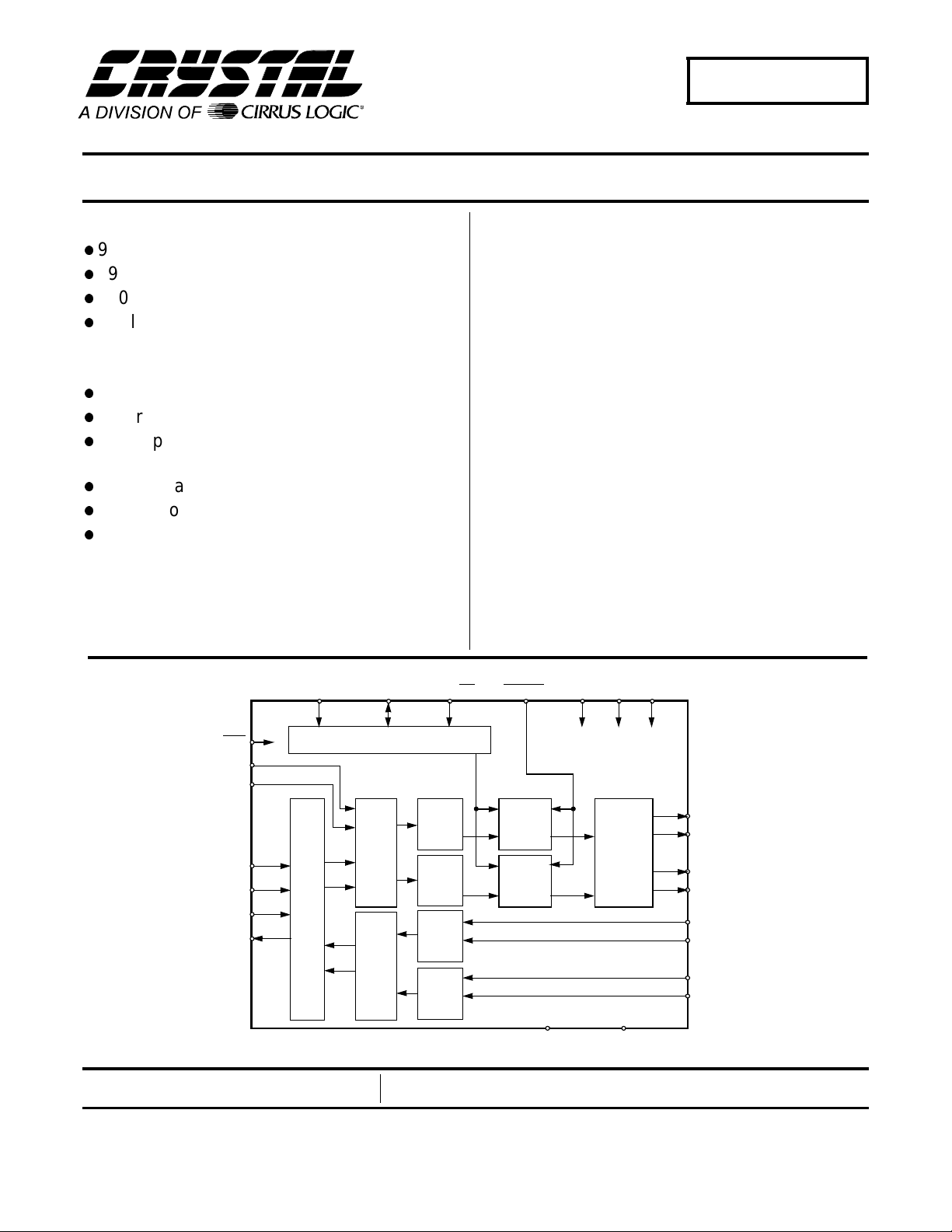
The CS4222 is a highly integrated, high performance,
20-bit, audio codec providing stereo analog-to-digital
and stereo digital-to-analog converters using delta-sigma conversion techniques. The device operates from a
single +5 V power supply, and features low power consumption. Selecta ble de- emphasis fil ter for 32, 44.1, and
48 kHz sample rates is also included.
The CS4222 also incl udes an analog volume control capable of 113.5 dB attenuation in 0.5 dB resolution. The
analog volume control architecture preserves dynamic
range during attenuation. Volume control changes are
implemented using a "soft" ramping or zero crossing
technique.
Applications include reverb processors, musical instruments, DAT, and multitrack recorders.
The CS4222 is packaged in a 28-pin plastic SSOP.
ORDERING INFORMATION
CS4222-KS -10° to +70° C 28-pin SSOP
CDB4222 Evaluation Board
SCL/CCLK
RST
DEM1
DEM0
LRCK
SCLK
SDIN
SDOUT
Serial Audio Da ta Interface
Preliminary Product Information
Cirrus Logic, Inc.
Crystal Semiconductor Products Division
P.O. Box 17847, Austin, Texas 78760
(512) 445 7222 FAX: (512) 445 7581
http://www.crystal.com
SDA/CDIN AD0/CS
Control Port
Left
DAC
Digital Filters
Digital Filters
Right
with De-Emphas i s
DAC
Left
ADC
Right
ADC
This document contains information for a new product.
Cirrus Logic reserves the right to modify this product without notice.
SMUTE VD
Volume
Control
Volume
Control
Copyright Cirrus Logic, I nc. 1997
(All Rights Reserv ed)
MCLK VA
DGND
Pass and
Analog Low
AGND
Output Stage
AOUTL+
AOUTL-
AOUTR+
AOUTR-
AINLAINL+
AINRAINR+
JAN ‘97
DS236PP3
1
CS4222
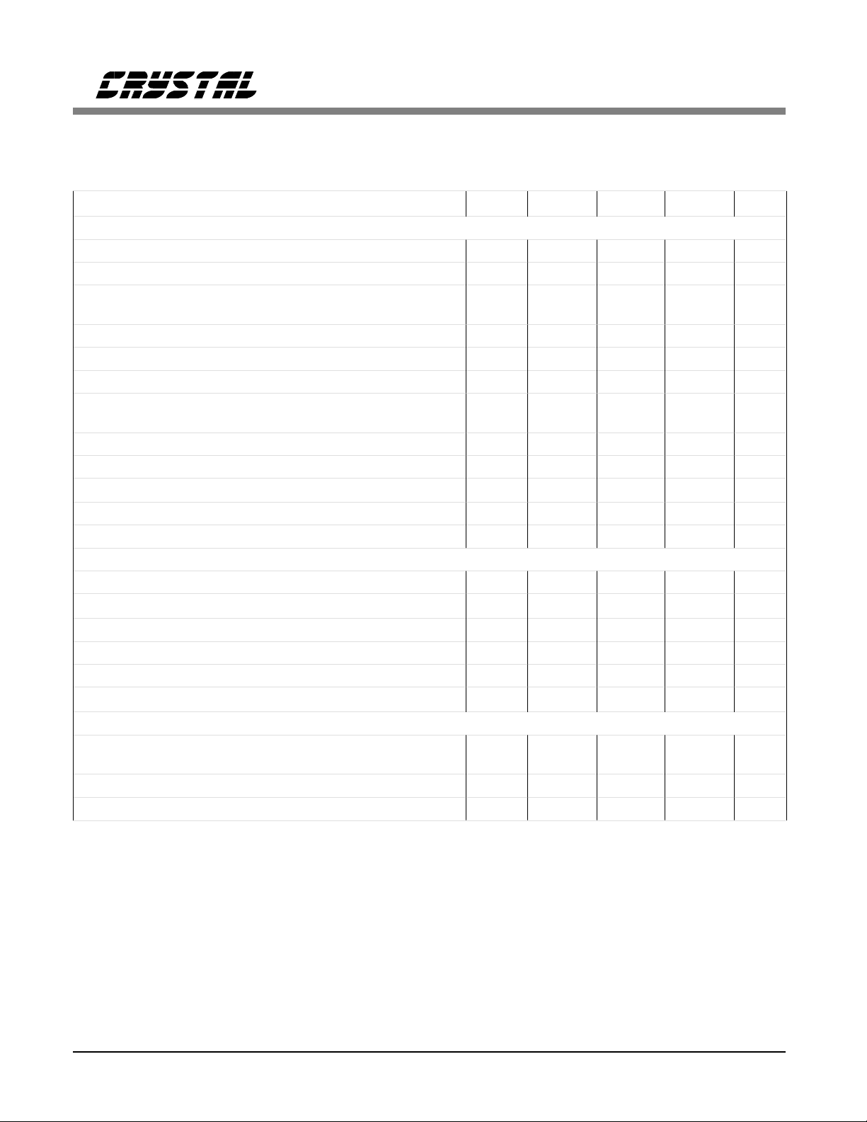
ANALOG CHARACTERISTICS
( TA = 25°C; VA, VD = +5V; Full Scale Input Sine wave,
997 Hz; Fs = 48 kHz; Measurement Bandwidth is 20 Hz to 20 kHz; Local components as shown in "Recommended Connection Diagram"; SPI mode, Format 0, unless otherwise specified.)
Parameter Symbol Min Typ Max Uni ts
Analog Input Characteristics
ADC Resolution - - 20 Bits
Total Harmonic Distortion THD 0.003 - %
Dynamic Range (A-weighted):
(unweighted):
TBD
TBD
99
96
-
-
dB
dB
Total Harmonic Distortion + Noise -1 dB (Note 1) THD+N - -90 TBD dB
Interchannel Isolation (1 kHz) - 90 - dB
Interchannel Gain Mismatch - 0.1 - dB
Offset Error (with High Pass Filter)
(HPF defeated with CAL)
-
-
-
TBD
0
-
LSB
LSB
Full Scale Input Voltage (Differential) 1.9 2.0 2.1 Vrms
Gain Drift - 100 - ppm/°C
Input Resistance 10 - -
kΩ
Input Capacitance - - 15 pF
Common Mode Input Voltage - 2.3 - V
A/D De ci mati on F ilt er C harac te rist ic s
Passband (Note 2) 0 - 21.8 kHz
Passband Ripple - -
±0.01
dB
Stopb and (Note 2) 30 - 6114 kHz
Stopb and Att enu ati on (Note 3) 80 - - dB
Group Delay (Fs = Output Sample Rate) (Note 4) t
Group Delay Variation vs. Frequency
∆ t
gd
gd
-15/Fs- s
--0
µs
High Pass Filter Characteristics
Frequency Response: -3 dB (Note 2)
-0.1 dB
-
-
3.7
20
-
-
Hz
Hz
Phase Dev iat ion @ 20 Hz (Note 2) - 10 - De gree
Passband Ripple - - 0 dB
Notes: 1. Referenced to typical full-scale differential input voltage (2 Vrms)
2. Filter characteristics scale with output sample rate. For output sample rates, Fs, other than 48 kHz,
the 0.01 dB passband edge is 0.4535xFs and the stopband edge is 0.625xFs.
3. The analog modulator samples the input at 6.144 MHz for an Fs equal to 48 kHz. There is
no rejection of input signals which are multiples of the sampling frequency ( n x 6.144 MHz ±21.8 kHz
where n = 0,1, 2, 3.. .).
4. Group delay for Fs = 48 kHz, t
= 15/48 kHz = 312µs
gd
* Parame ter de finit ions ar e give n at the end of thi s data s heet.
Specifications are subject to change without notice.
2 DS236PP3
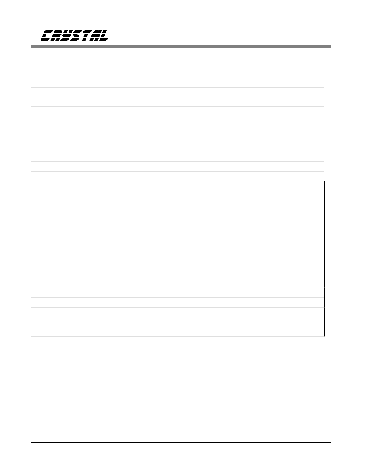
ANALOG CHARACTERISTICS (Continued)
Parameter Symbol Min Typ Max Units
CS4222
Analog Output Characteristics
DAC Resolution - - 20 Bits
Signal-to-Noise, Idle- Channel Noise ( DAC muted, A-weighted) TBD 110 - dB
Dynamic Range (DAC not muted, A-weighted)
Total Harmonic Distortion THD - 0.003 - %
Total Harmonic Distortion + Noise THD+N - -88 TBD dB
Interchannel Isolation (1kHz) - 90 - dB
Interchannel Gain Mismatch - 0.1 - dB
Attenuation Step Size (All Outputs) 0.35 0.5 0.65 dB
Programmable Output Attenuation Span 110 113.5 - dB
Differential Offset Voltage -
Common Mode Ou tput Vo lta ge - 2.3 - V
Full Scale Output Voltage 1.9 2.0 2.1 Vrms
Gain Drift - 100 - ppm/°C
Out-of-Band Energy (Fs/2 to 2Fs) - -60 - dBFS
Analog Output Load Resistance:
- Minimum Attenuation, 10 kΩ, 100 pF load; unless otherwise specified.
(DAC not muted, unweighted)
Capacitance:
TBD
TBD
10
-
99
96
±10
-
-
-
-
-mV
-
100
dB
dB
kΩ
pF
Combined Digital and Analog Filter Characteristics
Frequency Response 10 Hz to 20 kHz Deviation from Linear Phase Passband: to 0.01 dB corner (Notes 5,6) 0 - 21.8 kHz
Passband Ripple (Note 6) - Stopband (Notes 5,6) 26.2 - - kHz
Stopband Attenuation (Notes 7) 70 - - dB
Group Delay (Fs = Input Word Rate) t
gd
-16 / Fs- s
±0.1
±0.5
-dB
- Degrees
±0.01
dB
Power Supply
Power Supply Current VA
VD
Total Power Down
Power Supply Rejection Ratio (1 kHz, 10 mV
Notes: 5. The passband and stopband edges scale with frequency. For input word rates, Fs, other than
48 kHz, the 0.01 dB passband edge is 0.4535xFs and the stopband edge is 0.5465xFs.
6. Digital filter characteristics .
7. Measurement bandwidth is 10Hz to 3Fs.
)-50-dB
rms
-
-
-
30
20
0.2
TBD
TBD
-
mA
mA
mA
Specifications are subject to change without notice
DS236PP3 3
CS4222
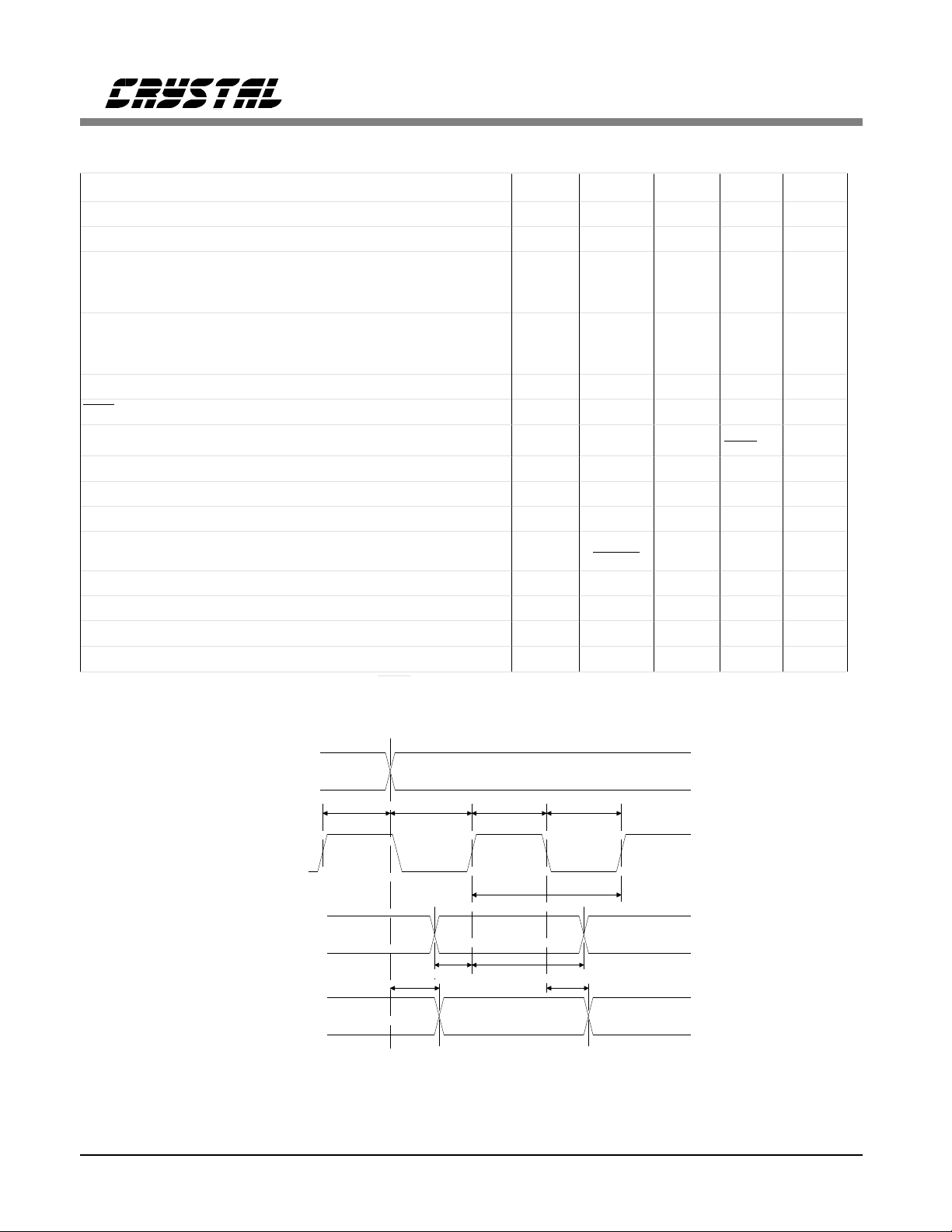
SWITCHING CHARACTERISTICS
(TA = 25°C; VA, VD = +5V ±5%, outputs loaded with 30pF)
Parameter Symbol Min Typ Max Units
Audio ADC’s & DAC’s Sample Rate Fs 4 - 50 kHz
MCLK Frequency (MCLK = 256, 384, or 512 Fs) 1.024 - 26 MHz
MCLK Pulse Width High MCLK = 512 Fs
MCLK = 384 Fs
MCLK = 256 Fs
MCLK Pulse Width Low MCLK = 512 Fs
MCLK = 384 Fs
MCLK = 256 Fs
10
21
31
10
21
31
-
-
-
-
-
-
-
-
-
-
-
-
ns
ns
ns
ns
ns
ns
MCLK Jitter Tolerance - 500 - ps RMS
RST Lo w Ti me (Note 8) 10 - - ms
SCLK Falling edge to SDOUT output valid (DSCK=0 ) t
LRCK edge to MSB valid t
SDIN Setup Time Before SCLK Rising Edge (DSCK=0) t
SDIN Hold Time After SCLK Rising Edge (DSCK=0) t
SCLK Period t
SCLK High Time t
SCLK Low Time t
SCLK Rising to LRCK Edge (DSCK=0) t
LRCK Edge to SCLK Rising (DSCK=0) t
dpd
lrpd
ds
dh
sckw
sckh
sckl
lrckd
lrcks
--
- - 25 ns
- - 25 ns
- - 25 ns
1
(128) Fs
--ns
40 - - ns
40 - - ns
20 - - ns
40 - - ns
1
(384)
Fs
+ 20 ns
Notes: 8. After powering up the CS4222, PDN should be held low for 10 ms to allow the power supply
to settle.
LRCK
t
lrckd
SCLK*
SDIN
SDOUT
*SCLK shown for DSCK = 0, SCLK inve rt ed f or DSCK = 1.
t
lrpd
t
lrcks
t
ds
t
sckh
t
dh
MSB
t
sckw
t
sckl
t
dpd
MSB-1
Serial Audio Port Data I/O timing
4 DS236PP3
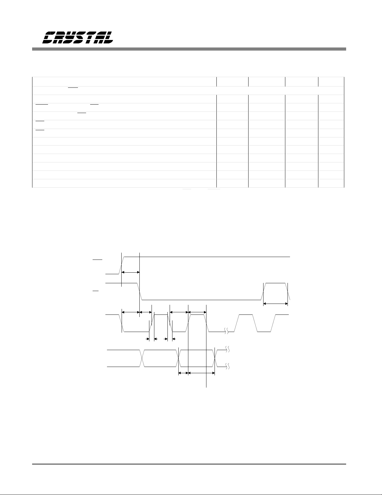
SWITCHING CHARACTERISTICS - CONTROL PORT
(TA = 25°C VD, VA = 5V±5%; I nputs: logic 0 = DGND, logic 1 = VD, CL = 30pF)
Parameter Symbol Min Max Units
SPI Mode (SPI/I2C = 0)
CCLK Clock Frequency f
RST rising edge to CS falling t
CCLK edge to
CS falling (Note 9) t
CS High Time Between Transmissions t
CS Falling to CCLK Edge t
CCLK Low Time t
CCLK High Time t
CDIN to CCLK Rising Setup Time t
CCLK Rising to DATA Hold Time (Note 10) t
Rise Time of CCLK and CDIN (Note 11) t
Fall Time of CCLK and CDIN (Note 11) t
Notes: 9. t
only needed before first falling e dge of CS a fter RST rising edge.
spi
= 0 at all other times.
t
spi
10. Data must be held for sufficient time to bridge the transition time of CCLK.
11. For F
< 1 MHz
SCK
sck
srs
spi
csh
css
scl
sch
dsu
dh
r2
f2
CS4222
-6MHz
500 - ns
500 - ns
1.0 20 - ns
66 - ns
66 - ns
40 - ns
15 - ns
- 100 ns
- 100 ns
µs
RST
CS
CCLK
CDIN
t
t
srs
spi
t
t
r2
css
t
scl
t
t
f2
dsu
t
sch
t
dh
t
csh
DS236PP3 5
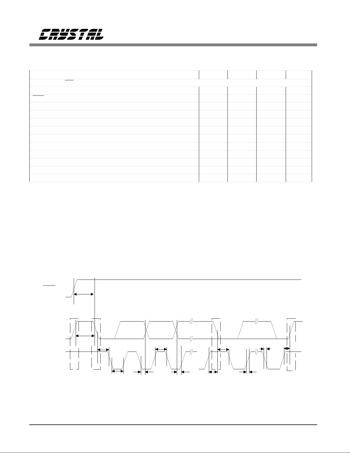
SWITCHING CHARACTERISTICS - CONTROL PORT
(TA = 25°C; VD, VA = 5V±5%; Inputs: logic 0 = DGND, logic 1 = VD, CL = 30pF)
Parameter Symbol Min Max Units
I2C® Mode (SPI/I2C = 1) (Note 12 )
SCL Clock Frequency f
RST Rising Edge to Start t
Bus Free Time Between Transmissions t
Start Condition Hold Time (prio r to first clock pulse) t
Clock Low Time t
Clock High Time t
Setup Time for Repeated Start Condition t
SDA Hold Time from SCL Falling (Note 13) t
SDA Setup Time to SCL Rising t
Rise Time of Both SDA and SCL Lines t
Fall Time of Both SDA and SCL Lines t
Setup Time for Stop Condition t
2C®
Notes: 12. Use of the I
2C®
is a registered trad emark of Philips Semicon ductors.
I
bus interface requires a license f rom Philips.
13. Data must be held for sufficient time to bridge the 300ns transition time of SCL.
scl
irs
buf
hdst
low
high
sust
hdd
sud
r
f
susp
CS4222
- 100 kHz
500 - ns
4.7 -
4.0 -
4.7 -
4.0 -
4.7 0-
250 - ns
-1
- 300 ns
4.7
µs
µs
µs
µs
µs
µs
µs
µs
RST
t
irs
Repeated
Stop
Start
Start
Stop
SDA
t
buf
t
hdst
t
high
t
hdst
t
f
t
susp
SCL
t
low
t
hdd
t
sud
t
sust
t
r
6 DS236PP3
CS4222
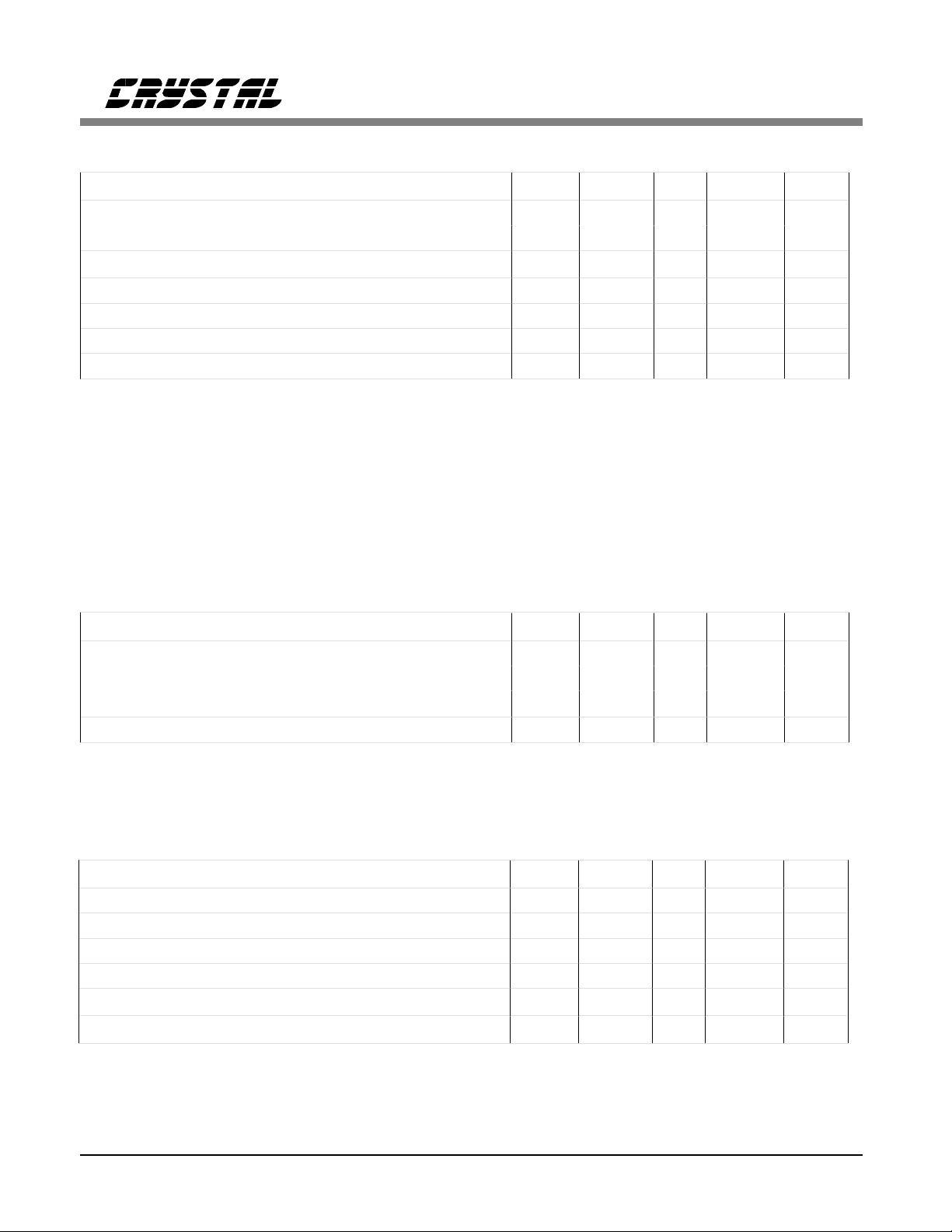
ABSOLUTE MAXIMUM RATINGS (AGND, DGND = 0V, all voltages with respect to 0V.)
Parameter Symbol Min Typ Max Units
Power Supplies Digital VD -0 .3 - 6.0 V
Analog VA -0.3 - 6.0 V
Input Current (Note 14) - -
±10
Analog Input Voltage (Note 15) -0.7 - VA+0.7 V
Digital Input Voltage (Note 15) -0.7 - VD+0.7 V
Ambient Temperature (Power Applied) -55 - +125 °C
Storage Temperature -65 - +150 °C
Warning: Operation at or beyond these limits may result in permanent damage to the device.
Normal operation is not guaranteed at these extremes.
Note: 14. Any pin except supplies. Transient currents of up to ±100mA on the analog input pins will
not cause SCR latch-up.
15. The maximum over or under voltage is limited by the input current.
mA
RECOMMENDED OPERATING CONDITIONS ( AGND, DGND = 0V, all voltages with respect
to 0V.)
Parameter Symbol Min Typ Max Units
Power Supplies Digital VD 4.75 5.0 5.25 V
Analog VA 4.75 5.0 5.25 V
VA - VD
Operating Ambient Temperature T
A
--0.4V
-10 25 70 °C
DIGITAL CHARACTERISTICS (TA = 25 °C; VA, VD = 5V ± 5%)
Parameter Symbol Min Typ Max Units
High-level Input Voltage V
Low-level Input Voltage V
High-level Output Voltage at I
Low-level Output Voltage at I
= -2.0 mA V
0
= 2.0 mA V
0
IH
IL
OH
OL
Input Leakage Current (Digital Inputs) - - 10
Output Leakage Current (High Impedance Digital Outputs) - - 10
2.8 - VD+0 .3 V
-0.3 - 1. 0 V
VD-1.0 - - V
--0.4V
µA
µA
DS236PP3 7
CS4222
Ferrite Bead
+5V
Supply
150
150
150
150
Microcontroller
Note: Pins 10,11, and 12
should be tied to DGND
in stand -a lo ne mode.
+ 0.1 µF
1 µF
Ω
20
AINL+
2.2 nF
Ω
19
AINL-
Ω
17
AINR+
2.2 nF
Ω
16
AINR-
10
SCL/CCLK
11
SDA/CDIN
12
AD0/CS
27
RST
2
SMUTE
1
NC
14
NC
15
NC
28
NC
Ω
2
21
VA
6
VD
AOUTL+
AOUTL-
AOUTR+
AOUTR-
CS4222
DEM1
DEM0
SDOUT
LRCK
SCLK
MCLK
AGND DGND
22 7
SDIN
0.1 µF + 1 µF
25
26
24
23
18
13
8
9
4
5
3
Analog
Filter
Analog
Filter
Digital
Audio
Source
R
s
R
s
R
s
R
s
R
s
Audio
DSP
1
R = 500
s
R = 50
s
1
Ω
Ω
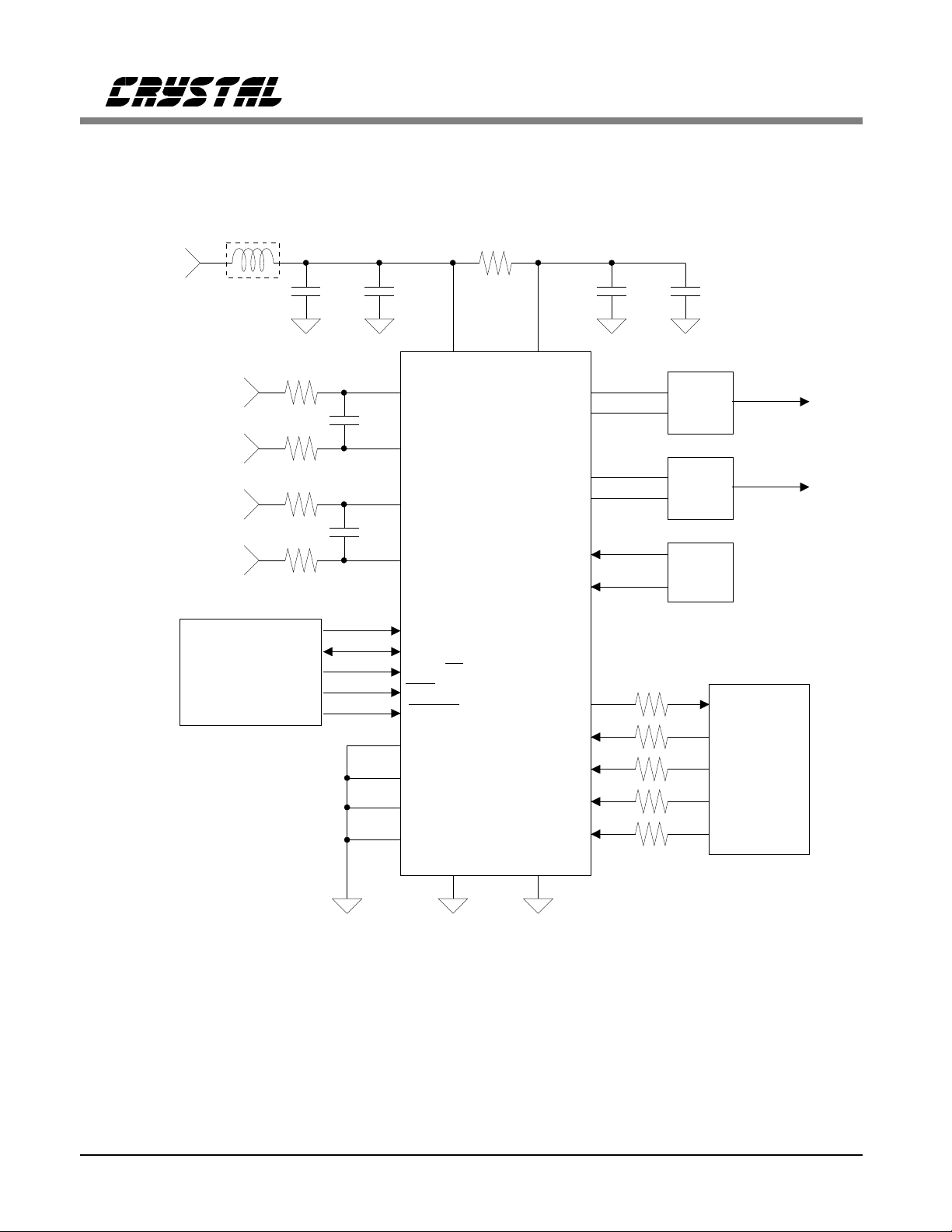
Figure 1. Recommended Connecti on Diagra m
(Also see reco mmen ded l ayo ut d iag ram, Fi gure 10)
8 DS236PP3
 Loading...