

16-Bit Stereo Audio Codec
CS4218
Complete CMOS Stereo Audio Input
and Output System featuring:
Delta-Sigma A/D and D/A Converters using
•
64x Oversampling.
Input Anti-Aliasing and Output Smoothing
•
Filters.
Programmable Input Gain (0 dB to 22. 5 dB).
•
Programmable Output Attenuation (0 dB to
•
46.5 dB).
Sample frequencies from 4 kHz to 50 kHz.
•
Low Distortion, THD < 0.02% for DAC.
•
THD < 0.02% for ADC.
Low Power Dissipation: 80 mA typical.
•
Power-Down Mode : 1 mA typical.
•
Pin Compatible with CS4216 when used in
•
Serial Modes 3 and 4 (See Appendix A).
I2S(TM) Compatible Serial Mode (SM5).
•
Operates from 5V or 3.3V Digital Power
•
Supply. Requires 5V Analog Power Supply.
General Description
The CS4218 Stereo Audio Codec is a monolithic
CMOS device for computer multimedia, automotive,
and portable audio applications. It performs A/D and
D/A conversion, filtering, and level setting, creating 4
audio inputs and 2 audio outputs for a digital computer
system. The digital interfaces of left and right channels
are multiplexed into a single serial data bus with word
rates up to 50 kHz per channel.
ADCs and the DACs use delta-sigma modulation with
64X oversampling. The ADCs and DACs include digital decimation filters and output smoothing filters
on-chip which eliminate the need for external anti-aliasing filters.
The CS4218 is pin and function compatible with the
CS4216 when used in Serial modes 3 and 4. See the
Appendix A at the end of this data sheet for details.
2
I
S is a trademark of Ph ilips.
Ordering Information:
CS4218-KL 0
CS4218-KQ 0
° to 70°C 44-pin PLCC
° to 70°C 44-pin TQFP
RESET
PDN
SMODE3
SMODE2
SMODE1
SDIN
SDOUT
SCLK
SSYNC
MF7:SFS1/F2
MF8:SFS2/F3
FILT
CLKIN
Crystal Semiconductor Corporation
P.O. Box 17847, Austin, TX 78760
(512) 445 7222 FAX: (512) 445 7581
http://www.crystal.com
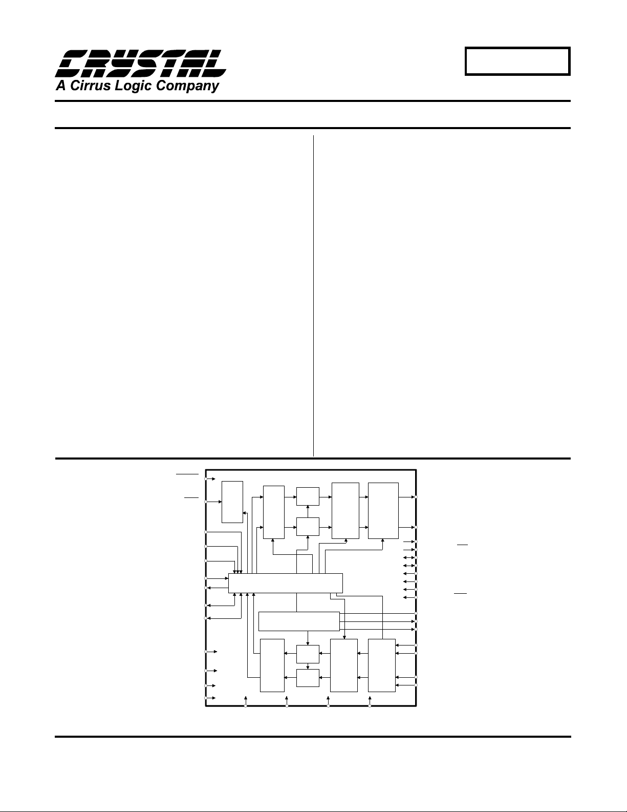
D/A
POWER
CONTROL
SERIAL INTERFACE CONTROL
VD VA
DIGITAL
FILTERS
D/A
VOLTAGE REFERENCE
A/D
DIGITAL
FILTERS
A/D
DGND AGND
Copyright Crystal Semiconductor Corporation 1996
OUTPUT
MUTE
OUTPUT
ATTENUATION
INPUT
GAIN
INPUT
MUX
(All Rights Reserved)
LOUT
ROUT
DO1
MF5:DO2/INT
MF2:F2/CDIN
MF1:F1/CDOUT
DI1
MF6:DI2/F1
MF3:DI3/F3/CCLK
MF4:MA/CCS
REFGND
REFBYP
REFBUF
LIN1
LIN2
RIN1
RIN2
SEP ’96
DS135F1
1

Contents
Description
Cover . . . . . . . . . . . . . . . . . . . . 1
Contents . . . . . . . . . . . . . . . . . . . 2
Recommended Operating Conditions . . . . . . . . . . . . 3
Analog Input Characteristics . . . . . . . . . . . . . . 3
Analog Output Characteristics . . . . . . . . . . . . . 4
Switching Characteristics . . . . . . . . . . . . . . . 5
Digital Characteristics . . . . . . . . . . . . . . . . 7
A/D Decimation Filter Characteristics . . . . . . . . . . . . 8
D/A Interpolation Characteristics . . . . . . . . . . . . . 8
Absolute Maximum Ratings . . . . . . . . . . . . . . 8
Filter Response Plots . . . . . . . . . . . . . . . . 9
Typical Connection Diagram . . . . . . . . . . . . . . 11
Overview . . . . . . . . . . . . . . . . . . . 12
Functional Description . . . . . . . . . . . . . . . 12
Serial Interface Modes . . . . . . . . . . . . . . . 15
Power Supply and Grounding . . . . . . . . . . . . . . 26
Pin Diagrams and Descriptions . . . . . . . . . . . . . 29
Package Information . . . . . . . . . . . . . . . . 35
Parameter Definitions . . . . . . . . . . . . . . . . 36
Appendix A: CS4218 Compatibility with the CS4216 . . . . . . . . 38
Appendix B: Applications of Serial Mode 4 (SM4) . . . . . . . . 40
Appendix C: Setting CLKIN/SCLK Ratio for Desired Sample Rate . . . . 43
CS4218
- Analog Inputs and Outputs . . . . . . . . . . . . . 12
- Offset Calibration . . . . . . . . . . . . . . . 13
- Input Gain and Output Level Setting . . . . . . . . . . 13
- Muting and the ADC Valid Counter . . . . . . . . . . . 13
- Parallel Digital I/O Pins . . . . . . . . . . . . . . 13
- Reset and Power Down Modes . . . . . . . . . . . . 13
- Audio Serial Interface . . . . . . . . . . . . . . 14
- Serial Mode 3 . . . . . . . . . . . . . . . . 15
- Serial Mode 4 . . . . . . . . . . . . . . . . 22
- Serial Mode 5 . . . . . . . . . . . . . . . . 25
2 DS135F1
CS4218
RECOMMENDED OPERATING CONDITIONS (AGND, DGND = 0V, all voltages with respect
to 0V.)
Parameter Symbol Min Typ Max Units
Power Supplies: Digital VD 4.75 5.0 5.25 V
Digital (Low Voltage) VD 3.0 3.3 3.6 V
Analog VA 4.75 5.0 5.25 V
Operating Ambient Temperature T
ANALOG CHARACTERISTICS( T
Logic 1 = VD; 1kHz Input Sine Wave; CLKIN = 12.288 MHz; SM3 Slave sub-mode, 256 BPF; 0dB gain/attenuation;Conversion Rate = 48 kHz; SCLK = 12.288 MHz; Measurement Bandwidth is 10 Hz to 20 kHz ; Unless otherwise specified.)
Parameter * Symbol Min Typ Max Units
Analog Input Characteristics - Minimum gain s etting (0 dB); unless otherwise specified.
ADC Resolution 16 - - Bits
ADC Differential Nonlinearity (Note 1) - - ±0.9 LSB
Instantaneous Dynamic Range (Note 3) IDR 80 84 - dB
Total Harmonic Distortion THD - - 0.02 %
Interchannel Isolation - 80 - dB
Interchannel Gain Mismatch - - ±0.5 dB
Frequency Response (Note 1) -0.5 - +0.2 dB
= 25°C; VA, VD = +5V; Input Levels: Logic 0 = 0V,
A
A
02570°C
Programmable Input Gain - 22.5 - dB
Gain Step Size - 1.5 - dB
Absolute Gain Step Error - - 0.75 dB
Gain Drift (Note 1) - 100 - ppm/°C
Offset Error 0dB Gain - - ±50 LSB
22.5dB Gain Full Scale Input Voltage 2.5 2.8 3.1 V
Input Resistance (Notes 1,2) 20 - - kΩ
Input Capacitance (Note 1) - - 15 pF
Notes: 1. This specification is guar anteed by characterization, not production testing.
2. Input resistance is for the input selec ted. Non-selected inputs have a very high (>1M
3. Operation in Slave sub-modes may yield results lower than the 80 dB minimum.
* Parameter definitions are given at the end of this data sheet.
Specifications are subject to change without notice.
DS135F1 3
−±500 LSB
pp
Ω) input resistance.
CS4218
ANALOG CHARACTERISTICS (Continued)
Parameter * Symbol Min Typ Max Units
Analog Output Characteristics - Minimum A ttenuation; Unless Otherwise Spec ified.
DAC Resolution 16 - - Bits
DAC Differential Nonlinearity (Note 1) - - ±0.9 LSB
Total Dynamic Range TDR - 93 - dB
Instantaneous Dynamic Range IDR 80 83 - dB
Total Harmonic Distortion (Note 4) THD - - 0.02 %
Interchannel Isolation (Note 4) - 80 - dB
Interchannel Gain Mismatch - - ±0.5 dB
Frequency Response (Note 1) -0.5 - +0.2 dB
Programmable Attenuation (Note 5) - -46.5 - dB
Attenuation Step Size (Note 5) - 1.5 - dB
Absolute Attenuation Step Error (Note 5) - - 0.75 dB
Gain Drift (Note 1) - 100 - ppm/°C
REFBUF Output Voltage (Note 6) 1.9 2.1 2.3 V
Maximum output current= 400
Offset Voltage (Note 7) - 10 - mV
Full Scale Output Voltage (Note 4) 2.4 2.7 3.1 V
External Load Impedance 10k - - Ω
Internal Resistor Value for LOUT and ROUT 400 600 800 Ω
Deviation from Linear Phase (Note 1) - - 1 Degree
Out of Band Energy (22 kHz to 100 kHz) - -60 - dB
Power Supply
Power Supply Current (Note 8) Operating (VD = 5.0V) - 80 100 mA
Operating (VD = 3.3V) - 65 85 mA
Power Down - - 1 mA
Power Supply Rejection (1 kHz) - 40 - dB
Notes: 4. 10 k
5. Tested in SM3, Slave sub-mode, 256 BPF.
6. REFBUF load current must be DC. To drive dynamic loads, REFBUF must be buffered.
7. No DC load.
8. Typical current: VA = 30mA, VD = 50mA with VD = 5.0V. VA = 30mA, V D = 35mA with VD = 3.3V.
Ω, 100 pF load.
AC variations in REFBUF current may degrade ADC and DAC performance.
Power supply current does not include output loading.
µA
pp
* Parameter definitions are given at the end of this data sheet.
4 DS135F1
CS4218
SWITCHING CHARACTERISTICS (T
Levels: Logic 0 = 0V, Logic 1 = VD)
Parameter Symbol Min Typ Max Units
Input clock (CLKIN) frequency SM3 Multiplier Mode CLKIN 64 768 800 KHz
SM3 Master and Slave Modes, SM4, SM5 CLKIN 1.024 12.288 12.8 MHz
CLKIN low time t
CLKIN high time t
Sample Rate (Note 1) Fs 4 - 50 kHz
DI pins setup time to SCLK edge (Note 1) t
DI pins hold time from SCLK edge (Note 1) t
DO pins delay from SCLK edge t
SCLK and SSYNC output
delay from CLKIN rising
SCLK period All master Modes (Notes 1,7) t
SCLK high time Slave Mode t
SCLK low time Slave Mode t
SDIN, SSYNC setup time to SCLK edge Slave Mode t
SDIN, SSYNC hold time from SCLK edge Slave Mode t
SDOUT delay from SCLK edge t
Output to Hi-Z state bit 64 (Note 1) t
Output to non-Hi-Z bit 1 (Note 1) t
RESET pulse width low 500 - - ns
All master Modes (Note 1) t
= 25°C; VA, VD = +5V, outputs loaded with 30 pF; Input
A
ckl
ckh
s2
h2
pd2
pd3
sckw - 1/(Fs*bpf) - s
Slave Mode
sckh
sckl
s1
h1
pd1
hz
nz
15 - - ns
15 - - ns
10 - - ns
8--ns
- - 30 ns
- - 50 ns
75 - - ns
30 - - ns
30 - - ns
15 - - ns
10 - - ns
- - 28 ns
- - 12 ns
15 - - ns
CCS low to CCLK rising SM4 (Note 1) t
CDIN setup to CCLK falling SM4 (Note 1) t
CCLK low to CDIN invalid (hold time) SM4 (Note 1) t
CCLK high time SM4 (Note 1) t
CCLK low time SM4 (Note 1) t
CCLK Period SM4 (Note 1) t
CCLK rising to CDOUT data valid SM4 (Note 1) t
CCLK rising to CDOUT Hi-Z SM4 (Note 1) t
CCLK falling to CCS high SM4 (Note 1) t
RESET low time prior to PDN rising trph 100 - - ns
RESET low hold time after PDN rising trhold 50 - - ms
Notes: 7. When the CS4218 is in master modes (SSYNC and SCLK outputs), the SCLK duty cycle is 50%.
The equation is based on the selected sample frequency (Fs) and the number of bits per frame (bpf).
DS135F1 5
cslcc
discc
ccdih
cclhh
cclhl
cclkw
ccdov
ccdot
cccsh
25 - - ns
15 - - ns
10 - - ns
25 - - ns
25 - - ns
75 - - ns
- - 30 ns
- - 30 ns
0--ns
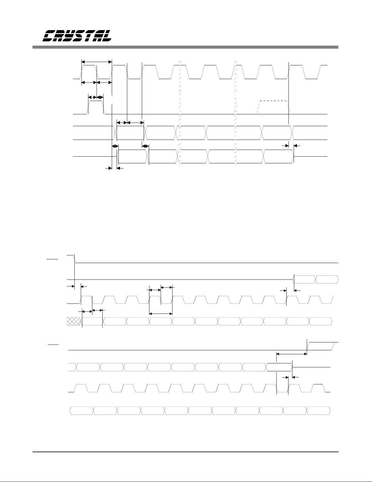
SCLK
[SM3,SM4\
SSYNC
[SM3,SM4\
SDIN
SDOUT
t
sckhtsckl
t
s1
[SM3]
(SM4)
[SM3]
(SM4)
t
sckw
CS4218
t
h1
t
t
h1
s1
Bit 1 Bit 2
t
pd1
Bit 1
t
nz
Bit 32
(Bit 32)
t
pd1
Bit 2
Bit 32
(Bit 32)
Serial Audio Port Timing
Bit 33
(Bit 1)
Bit 33
(Bit 1)
Bit 63
(Bit 31)
Bit 63
(Bit 31)
Bit 64
(Bit 32)
Bit 64
(Bit 32)
t
hz
MF4:CCS
MF1:CDOUT
MF3:CCLK
MF2:CDIN
MF4:CCS
MF1:CDOUT
MF3:CCLK
MF2:CDIN
t
discc
ADV
t
cslcc
t
ccdih
0MSK
t
cclkh
DO1
LAtt4
t
cclkl
t
cclkw
LAtt3
LAtt2
LAtt1
LAtt0
RAtt4
t
RAtt3
123 5 89467 10
0
DI1
ADV
0
t
ccdot
0000
0
RGain2
RGain1
0
RGain0
1
Err1
Err0
LCL RCL
0
24 28 29 3231302726252322
Serial Mode 4. Control Data Serial Port Timing
ccdov
RAtt2
t
cccsh
LCL
11
0
6 DS135F1
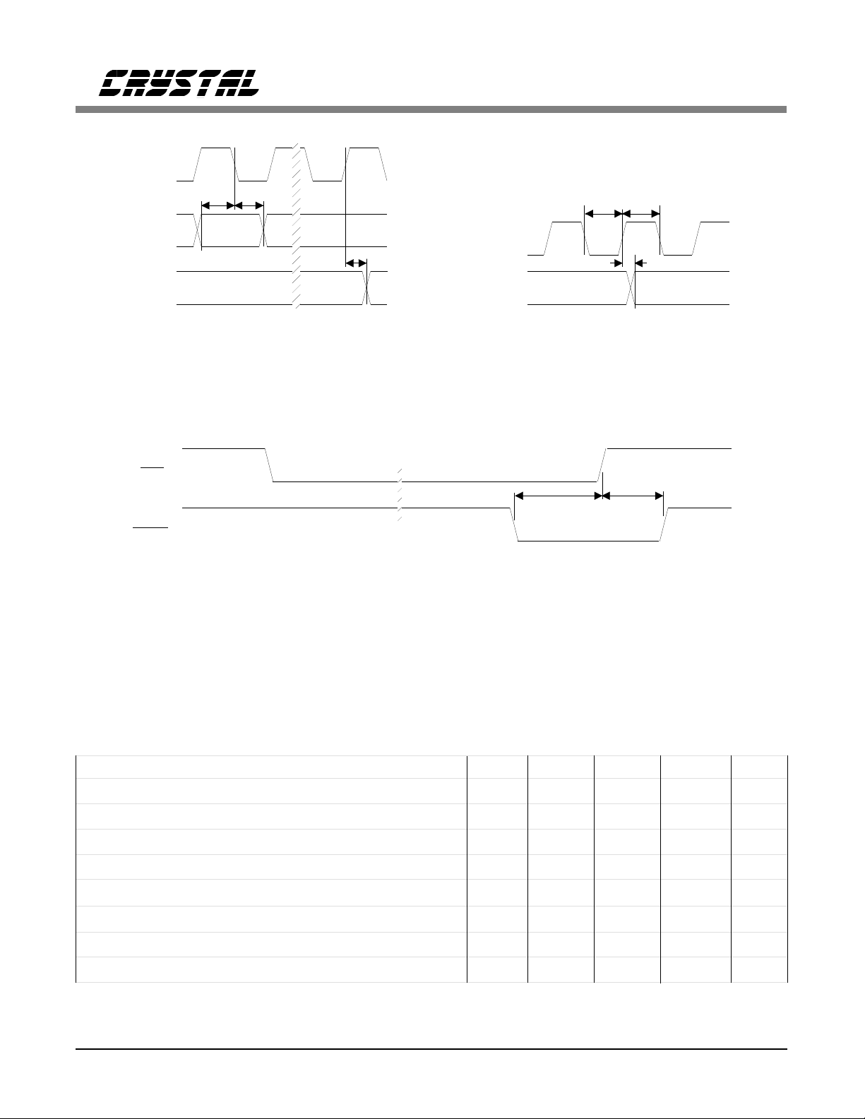
SCLK
CS4218
t
t
s2
h2
t
ckl
t
ckh
DIx
DOx
PDN
RESET
DI/DO Timing
CLKIN
t
pd2
SCLK
SSYNC
(Master Mode)
Power Down Mode Timing
t
pd3
SCLK & SSYNC Output Timing
(Master Mode)
t
rhold
t
rph
DIGITAL CHARACTERISTICS (T
= 25°C; VA = 5V, VD = 5V or 3.3V)
A
Parameter Symbol Min Typ Max Units
High-level Input Voltage V
Low-level Input Voltage V
High-level Output Voltage at I0 = -2.0 mA V
Low-level Output Voltage at I0 = +2.0 mA V
IH
IL
OH
OL
2.0 - VD+0 .3 V
-0.3 - 0.8 V
VD-0.3 - - V
--0.2V
Input Leakage Current (Digital Inputs) - - 10 µA
Output Leakage Current (High-Z Digital Outputs) - - 10 µA
Output Capacitance (Note 1) C
Input Capacitance (Note 1) C
OUT
IN
- - 15 pF
- - 15 pF
DS135F1 7
CS4218
A/D Decimation Filter Characteristics
Parameter Symbol Min Typ Max Units
Passband 0 - 0.40Fs Hz
Frequency Response -0.5 - +0.2 dB
Passband Ripple (0-0.4Fs) - - ±0.1 dB
Transition Band 0.40Fs - 0.60Fs Hz
Stop Band 0.60Fs - - Hz
Stop Band Rejection 74 - - dB
Group Delay - 8/Fs s
Group Delay Variation vs. Frequency - 0.0 µs
D/A Interpolation Filter Characteristics
Parameter Symbol Min Typ Max Units
Passband 0 - 0.40Fs Hz
Frequency Response -0.5 - +0.2 dB
Passband Ripple (0-0.4Fs) - - ±0.1 dB
Transition Band 0.40Fs - 0.60Fs Hz
Stop Band 0.60Fs - - Hz
Stop Band Rejection 74 - - dB
Group Delay - - 8/Fs s
Group Delay Variation vs. Frequency - - 0.1/Fs µs
ABSOLUTE MAXIMUM RATINGS (AGND, DGND = 0V, all voltages with respect to 0V.)
Parameter Symbol Min Typ Max Units
Power Supplies: Digital VD -0.3 - 6.0 V
Analog VA -0.3 - 6.0 V
Input Current (Except Supply Pins) - - ±10.0 mA
Analog Input Voltage -0.3 - VA+0.3 V
Digital Input Voltage -0.3 - VD+0.3 V
Ambient Temperature (Power Applied) -55 - +125 °C
Storage Temperature -65 - +150 °C
Warning: Operation beyond thes e limits may result in permanent damage to the device.
Normal operation is not guaranteed at these extremes.
8 DS135F1
CS4218
10
0
-10
-20
-30
-40
-50
Magnitude (dB)
-60
-70
-80
-90
-100
0.0 0.1 0.2 0.3 0.4 0.5 0.6 0.7 0.8 0.9 1.0
Input Frequency (×Fs)
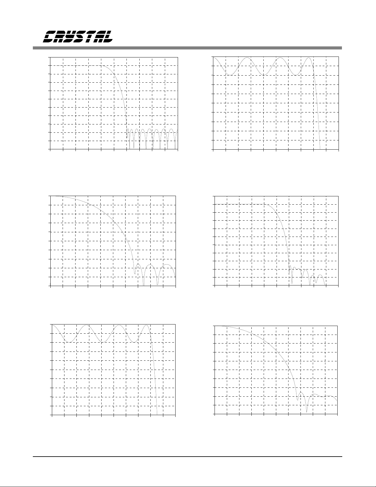
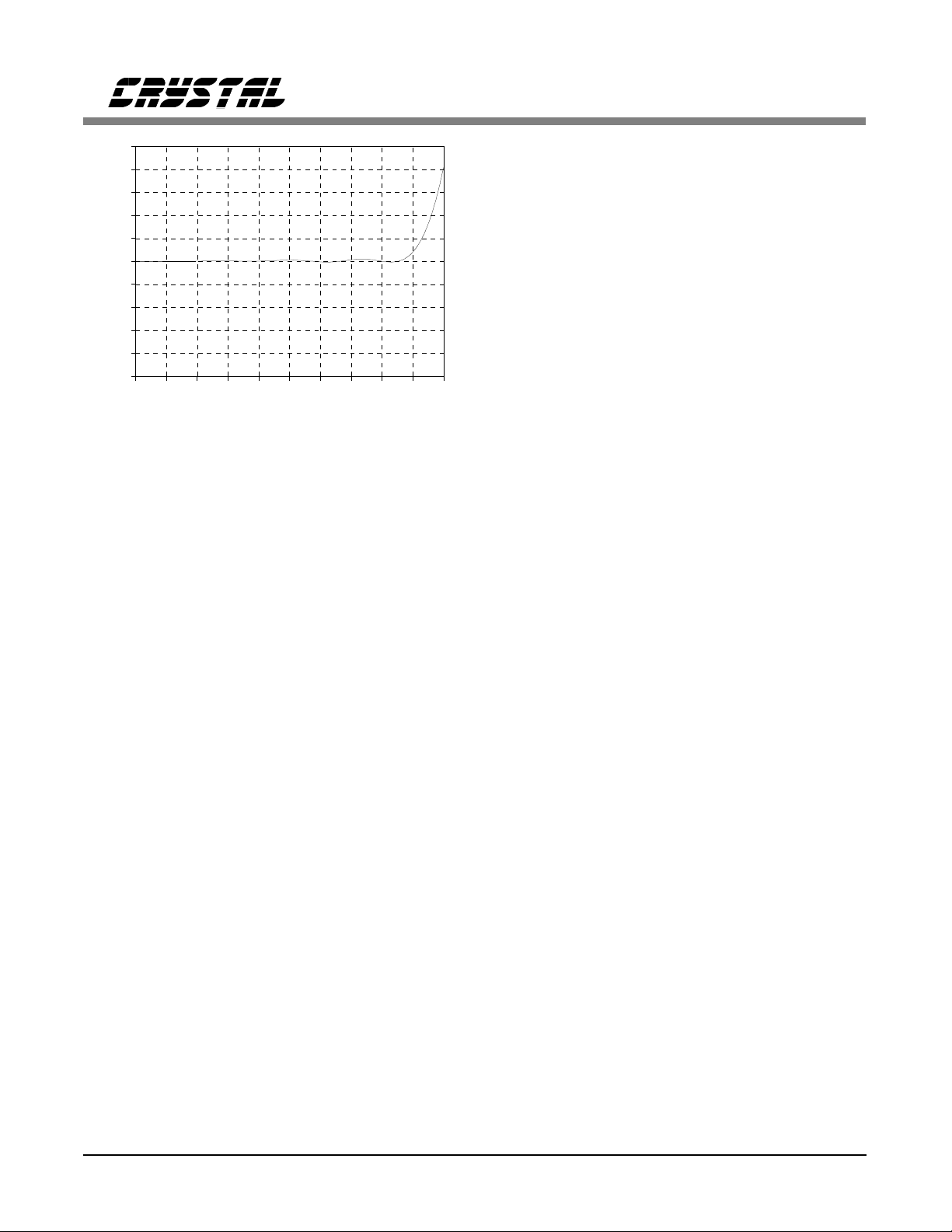
Figure 1. CS4218 ADC Frequency Response
0
-10
-20
-30
-40
-50
-60
Magnitude (dB)
-70
-80
-90
-100
0.40 0.43 0.46 0.49 0.52 0.55 0.58 0.61 0.64 0.67 0.70
Input Frequency (×Fs)
0.2
0.1
-0.0
-0.1
-0.2
-0.3
-0.4
Magnitude (dB)
-0.5
-0.6
-0.7
-0.8
0.00 0.05 0.10 0.15 0.20 0.25 0.30 0.35 0.40 0.45 0.50
Input Frequency (
Fs)
×
Figure 2. CS4218 ADC Passband Ripple
10
0
-10
-20
-30
-40
-50
-60
Magnitude (dB)
-70
-80
-90
-100
0.0 0.1 0.2 0.3 0.4 0.5 0.6 0.7
Input Frequency (
×
0.8
Fs)
0.9 1.0
Figure 3. CS4218 ADC Transition Band
0.2
0.1
-0.0
-0.1
-0.2
-0.3
-0.4
Magnitude (dB)
-0.5
-0.6
-0.7
-0.8
0.00 0.05 0.10 0.15 0.20 0.2 5 0.30 0.35 0.40 0.45 0.50
Input Frequency (×Fs)
Figure 5. CS4218 DAC Passband Ripple
Figure 4. CS4218 DAC Frequency Response
0
-10
-20
-30
-40
-50
-60
Magnitude (dB)
-70
-80
-90
-100
0.40
0.43
0.46
0.49 0.52
0.55 0.58 0.61
Input Frequency (×Fs)
Figure 6. CS4218 DAC Transition Band
0.64
0.67 0.70
DS135F1 9
2.5
2.0
1.5
1.0
0.5
0.0
-0.5
Phase (degrees)
-1.0
-1.5
-2.0
-2.5
0.00 0.05 0.10 0.15 0.20 0.25 0.30 0.35 0.40 0.45 0.50
Input Frequency (
Fs)
×
Figure 7. CS4218 DAC Deviation from Linear Phase
CS4218
10 DS135F1
CS4218
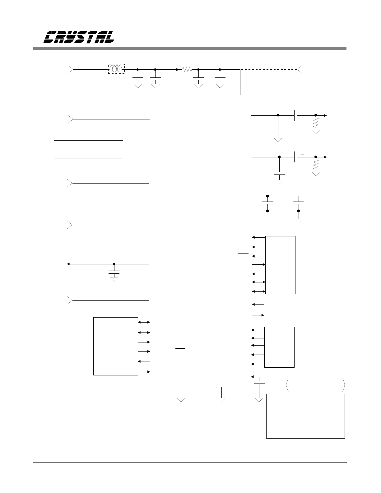
+5V
Supply
Line In 2
Right
See
for suggested input ciruits.
Line In 2
Left
Line In 1
Right
To Optional
Input Buffers
Line In 1
Left
Analog Inputs
Ferrit e Bead
1 µF
+
section
0.47µF
Parallel Bits
or
Sub-Mode
Settings
or
Control Port
Note: AGND and DGND pins MUST be on the same ground plane
0.1 µF
26
RIN2
28
LIN2
25
RIN1
20
REFBUF
27
LIN1
40
MF1:F1/CDOUT
39
MF2:F2/CDIN
35
MF3:DI3/F3/CCLK
36
MF4:MA/CCS
38
MF5:DO2/INT
34
MF6:DI2/F1
2.0
1 µF
+
4
CS4218
AGND DGND
23 5
0.1 µF
24
VAVD
ROUT
LOUT
REFBYP
REFGND
CLKIN
RESET
PDN
SDOUT
SDIN
SCLK
SSYNC
SMODE3
SMODE2
SMODE1
MF7:SFS1
MF8:SFS2
FILT
Figure 8. Typical Connection Diagram
+5V
Analog
If a separate +5V
Analog supply is used, remove
the 2.0 ohm resistor
15
16
21
22
3
2
13
43
42
44
1
33
37
41
32
29
31
30
6
0.1 µF
Controller
DI1
DO1
Mode
Setting
C
FILT
0.47µF
Refer to the
section for terminating
All other unused inputs
should be tied to GND. All NC
pins should be left floating.
> 1.0 µF
+
40 k
0.0022µF
NPO
> 1.0 µF
+
40 k
0.0022µF
NPO
+
µ
F
10
Required only for SM3
Multiplier Sub-Mode
Analog Inputs
unused line inputs.
Right
Audio
Output
Left
Audio
Output
DS135F1 11
OVERVIEW
CS4218
The CS4218 contains two analog-to-digital converters, two digital-to-analog converters,
adjustable input gain, and adjustable output level
control. Since the converters contain all the required filters in digital or sampled analog form,
the filters’ frequency responses track the sample
rate of the CS4218. Only a single-pole RC filter
is required for the analog inputs and outputs.
Communication with the CS4218 is via a serial
port, with separate pins for data input and output. The filters and converters operate over a
sample rate range of 4 kHz to 50 kHz.
FUNCTIONAL DESCRIPTION
Analog Inputs and Outputs
Figure 8 illustrates the suggested connection diagram for the CS4218. The line level inputs,
LIN1 or LIN2 and RIN1 or RIN2, are selected
by an internal input multiplexer. This multiplexer
is a source selector and is not designed for realtime switching between inputs at the sample rate.
When using the CS4218 as a drop-in replacement for the CS4216, existing recommended
circuits (shown in the CS4216 data sheet) may
be used as is without any noticeable degradation
in performance. Performance may vary with
user-specific input circuits and should be
checked when contemplating the use of CS4218
in existing CS4216 designs.
Unused analog inputs that are not selected have
a very high input impedance, so they may be
tied to AGND directly. Unused analog inputs
that are selected should be tied to AGND
through a 0.1 µF capacitor. This prevents any
DC current flow.
The analog inputs are single-ended and internally biased to the REFBUF voltage (nominally
0.33 uF
300 pF
NPO
NPO
300 pF
0.33 uF
RIN1
or
RIN2
LIN1
or
LIN2
Line In
Right
Line In
Left
5.6K
5.6K
5.6K
5.6K
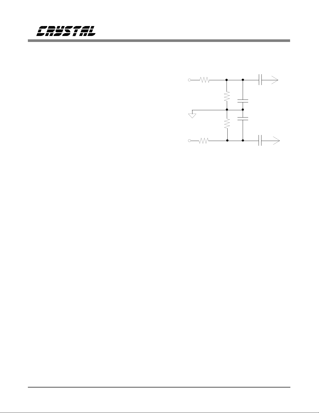
Figure 9. Line Inputs.
2.1 V). The REFBUF output should be buffered
if it is to be used for microphone phantom
power.
The use of a single-pole RC filter is recommended for use as an external anti-alias filter for
the CS4218. The maximum cutoff frequency
(lowpass) should not exceed 200 kHz. A lower
value for cuttoff frequency may be used, and is
dependent upon the application’s input bandwidth.
The CS4218 inputs will accept a 1Vrms signal,
so a divide by two resistor network will serve as
a front-end interface to 2 Vrms line level systems. Figure 9 shows a simple input circuit that
includes a gain of 0.5 and the required RC filter.
The gain of 0.5 yields a full scale input sensitivity of 2 V
with the CS4218 programmable
rms
gain set to 0.
The analog outputs are also single-ended and
centered around the REFBUF voltage. AC cou-
pling capacitors of >1 µF are recommended.
Refer to Figure 8 for the recommended analog
output circuit.
12 DS135F1
CS4218
When using the CS4218 as a drop-in replacement for the CS4216, the external 600 ohm
series resistors on LOUT and ROUT are not required, since they are part of the CS4218
internal circuitry.
In applications where both CS4218 and CS4216
are to be used, a board stuff option should be
included in the bill of materials which will allow
either a 600-ohm or a 0-ohm resistor to be used
externally on both LOUT and ROUT.
Offset Calibration
Both input and output offset voltages are minimized by internal calibration. Offset calibration
occurs after exiting a reset or power down condition. During calibration, which takes 194 frames,
output data from the ADCs will be all zeros, and
will be flagged as invalid. Also, the DAC outputs will be muted. After power down mode or
power up, RESET should be held low for a
minimum of 50 ms to allow the voltage reference to settle. Changing sample rates in master
and slave modes automaticall y initiates a calibration.
Input Gain and Output Level Settin g
Input gain is adjustable from 0 dB to +22.5 dB
in 1.5 dB steps. Output level attenuation is adjustable from 0 dB to -46.5 dB in 1.5 dB steps.
Both input and output gain adjustments are internally made on zero-crossings of the analog
signal, to minimize "zipper" noise. The gain
change automatically takes effect if a zero crossing does not occur within 512 frames.
Muting and the ADC Valid Counter
The mute function allows the the user to tu rn off
the output channels ( LOUT and ROUT ). Prior
to muting, the attenuation should be gradually
ramped to maximum ( 46.5 dB ), taking 1.5dB
steps. This significantly reduces any audible artifacts that may be heard once muting is enabled.
It is the users responsibility to program the serial
host to perform the ramping.
The serial data stream contains a "Valid Data"
indicator, the ADV bit, for the A/D converters
which is low until enough clocks have passed
since reset, or low-power (power down mode)
operation to have valid A/D data from the filters
(i.e., until calibration time plus the full latency
of the digital filters has passed.)
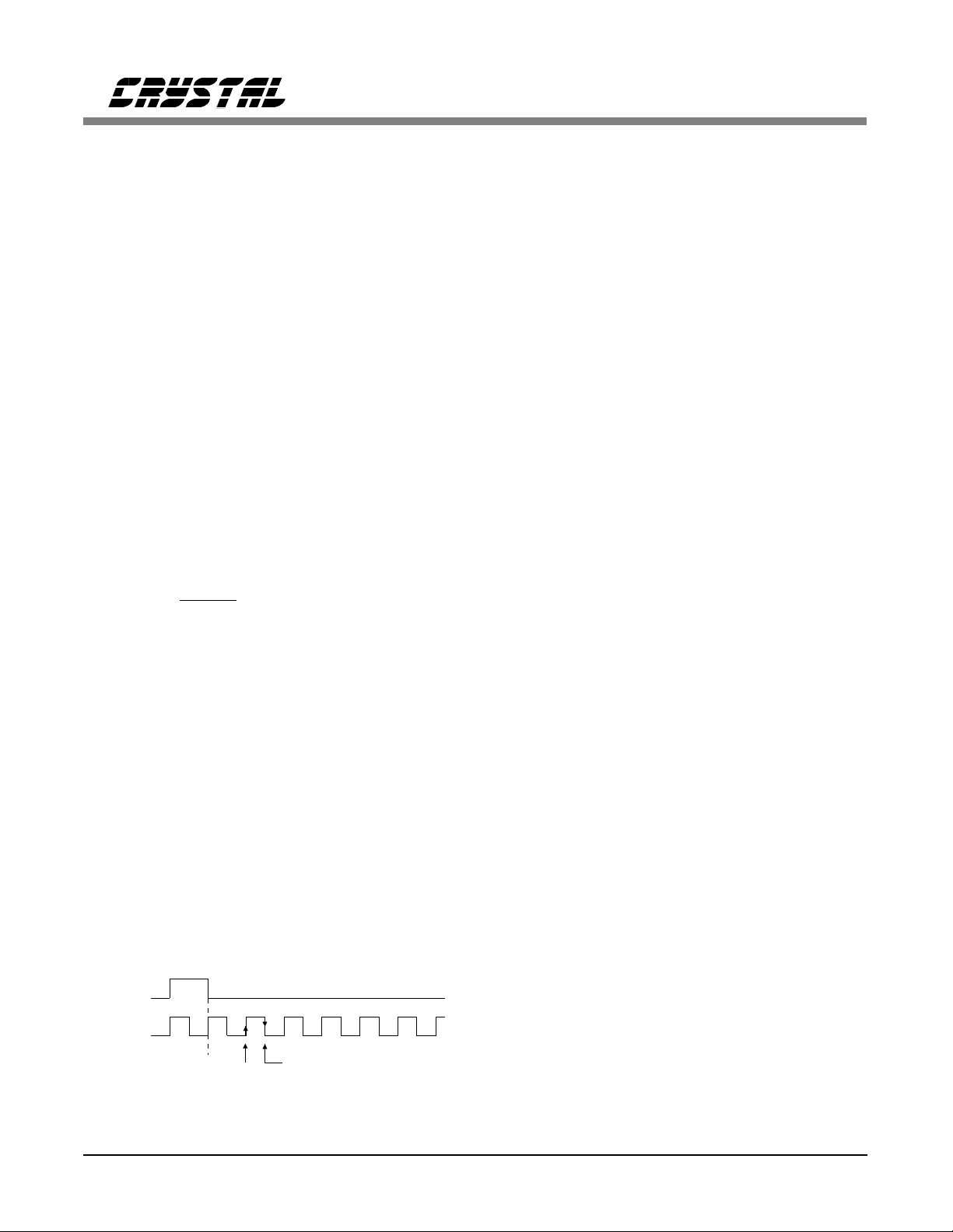
Parallel Dig ital Input/ Output Pin s
Parallel digital inputs are general purpose pins
whose values are reflected in the serial dat a output stream to the processor. Parallel digital
outputs provide a way to control external devices
using bits in the serial data input stream. All parallel digital pins, with the exception of DI1 and
DO1, are multifunction and are defined by the
serial mode selected. In Serial Mode 3 master
modes and Serial Mode 5, two digital inputs and
two digital outputs are available. In Serial Mode
3 slave modes, three digital inputs and two digital outputs are available. In Serial Mode 4 only
one digital input and digital output exists. Figure 10 shows when the DI pins are latched, and
when the DO pins are updated.
Reset and Power Down Modes
SSYNC
Reset places the CS4218 into a known state and
SCLK
(SM3)
Start of
Frame
Figure 10. Digital Input/Output Timing
DS135F1 13
DO pins
update
DI pins
latched
must be held low for at least 50 ms after powerup or a hard power down. In reset, the digital
outputs are driven low. Reset sets all control data
register bits to zero. Changing sample rates in
CS4218
master and slave modes automatically initiates a
calibration.
An RC filter with a time constant greater than
50 ms may be used on the RESET pin. The
CS4218 RESET pin has hysterisis to ensure
proper resets when using an RC filter.
Hard power down mode may be initiated by
bringing the PDN pin low. All analog outputs
will be driven to the REFBUF voltage which
will then decay to zero. All digital outputs will
be driven low and then will go to a high impedance state. Minimum power consumption will
occur if CLKIN is held low. After leaving the
power down state, RESET should be held low
for 50 ms to allow the analog voltage reference
to settle before calibration is started.
Alternatively, soft power down may be initiated
in slave modes by reducing the SCLK frequency
below the minimum values shown in Table 1. In
soft power down the analog outputs are muted
and the serial data from the codec will indicate
invalid data and the appropriate error code. The
parallel bit I/O is still functional in soft power
down mode. This is, in effect, a low power mode
with only the parallel bit I/O unit functioning.
Audio Serial Interface
In Serial Mode 3 (SM3), the audio serial port
uses 4 pins: SDOUT, SDIN, SCLK and SSYNC.
SDIN carries the D/A converters’ input data and
control bits. Input data is ignored for frames not
allocated to the selected CS4218. SDOUT carries the A/D converters’ output data and status
bits. SDOUT goes to a high-impedance state
during frames not allocated to the selected
CS4218. SCLK clocks data in to and out of the
CS4218. SSYNC indicates the start of a frame
and/or sub-frame. SCLK and SSYNC must be
synchronous to the master clock.
Serial Mode 4 (SM4 ) is similar to SM3 with the
exception of the control information. In Serial
Mode 4, the control information is entered
through a separate asynchronous control port.
Therefore, the audio serial port only contains
audio data, which reduces the number of bits on
the audio port from 64 to 32 per codec. This is
useful for lower bit rate serial hosts.
Serial Mode 5 (SM5) is compatible with the
I2STM serial data protocol. SM5 is a Master
mode only. As in SM3, 4 pins are used:
SDOUT, SDIN, SCLK, and SSYNC.
The serial port protocol is based on frames consisting of 1, 2, or 4 sub-frames. The frame rate is
the system sample rate. Each sub-frame is used
Bits Per Frame Minimum SCLK
Frequency
For All Modes Except SM3 Multiplier Sub Mode
32 CLKIN / 96
64 CLKIN / 48
128 CLKIN / 24
256 CLKIN / 12
SM3 Multiplier Sub Mode
64 (16 * CLKIN) / 48
128 (16 * CLKIN) / 24
256 (16 * CLKIN) / 12
by one CS4218 device. Up to 4 CS4218s may be
attached to the same serial control lines. SFS1
and SFS2 are tied low or high t o indicate to each
CS4218 which sub-frame is allocated for it to
use.
Serial Data Format
In SM3 and SM5, a sub-frame is 64 bits in
length and consists of two 16-bit audio values
and two 16-bit control fields. In SM4 a sub-
Table 1. Soft Power Down Conditions
(Slave Modes only)
frame is 32 bits in length and only contains the
two 16-bit audio fields; the control data is loaded
through a separate port. The audio data is MSB
14 DS135F1

CS4218
first, 2’s complement format. Sub-frame bit assignments are shown in Figure 13. Control data
bits all reset to zero.
CS4218 SERIAL INTERFACE MODES
The CS4218 has three serial port modes, selected
by the SMODE1, SMODE2 and SMODE3 pins.
In all modes, CLKIN, SCLK and SSYNC must
be derived from the same clock source. SM3
was designed as an easy interface to general purpose DSPs and provides features such as master
and slave sub-modes and variable frame sizes.
SM4 is similar to SM3 but splits the audio data
from the control data thereby reducing the audio
serial bus bandwidth by half. The control data is
transmitted through a control serial port in SM4.
SM5 is compatible with the I2S serial data protocol.
Table 2 lists the three serial port modes available, along with some of the differences between
modes. The first three columns in Table 2 select
the serial mode. The "SCLK Bit Center" column
indicates whether SCLK is rising or falling in
the center of a bit period. The "Sub-frame
Width" column indicates how many bits are in
an individual codec’s sub-frame. In SM3 and
SM4, the number of bits per frame is programmable. In all modes, SCLK and SSYNC must be
synchronous to the master clock. The last column in Table 2 lists the master frequencies used
by the codec. In the SM3 Multiplier sub-modes,
the master CLKIN is multiplied internally by 16,
so a 16xFs input clock must be provided.
SERIAL MODE 3, (SM3)
Serial Mode 3, Master and Slave sub-modes are
enabled by setting SMODE3 = 0, SMODE2 = 1
and SMODE1 = 0. SM3 Multiplier Sub-Modes
are enabled by setting SMODE 3 = 0, SMODE
2 = 0, and SMODE 1 = 0. Serial Mode 3 is designed to interface easily to DSPs.
Figure 11 illustrates the serial data in, SDIN,
sub-frame for all SM3 sub-modes. Figure 12
also illustrates the serial data out, SDOUT, subframe for all SM3 sub-modes. Figure 13 shows
sub-frame bit definitions.
In SM3 master sub-modes, MF5:DO2 is a general purpose output and MF6:DI2 is a general
purpose input. The other six multifunction pins
are used to select sub-modes under SM3. In
SM3 slave sub-modes, MF3:F3 is configured as
an additional general purpose input.
SM3 is divided into four sub-modes, Master
(SM3-M), Slave (SM3-S), Multiplier Master
(SM3-MM), and Multiplier Slave (SM3-MS).
SM3-M and SM3-S are identical to the CS4216
SM3 Master and Slave sub-modes, respectively.
In SM3-M and SM3-MM sub-modes, the
CS4218 generates SSYNC and SCLK, while in
SM3-S and SM3-MS sub-modes SSYNC and
SMODE PINS Serial SCLK Bit Sub-frame Bits per SCLK & Master
3 2 1 Mode Center Width Frame (BPF) SSYNC Frequency
0 0 0 SM3* Falling 64 bits 64/128/256 Master/S lave CLKIN = 16xFs
0 0 1 SM5 Rising 64 bits 64 Master CLKIN = 256xFs
0 1 0 SM3 F alling 64 bits 64/128/256 Master/Slave CLKIN or SCLK = 256×Fs
011 Factory Test mode
1 x x SM4 Falling 32 bits
†
Contains audio data only. Control information is entered through a separate serial port.
* SM3 Multiplier sub-modes.
DS135F1 15
†
32/64/128†Master/Slave CLKIN = 256×Fs
Table 2. Serial Port Modes

CS4218
SCLK must be generated externally. When the
codec is the serial port master, the serial port signal transitions are controlled with respect to the
internal analog sampling clock to minimize the
amount of digital noise coupled into the analog
section. Since SSYNC and SCLK are externally
derived when the codec slaves to the serial port,
optimum noise management cannot be obtained;
therefore, master modes should be used whenever possible. Multiplier sub-modes are identical
to the SM3 modes except the master clock,
CLKIN, is internally multiplied by 16. A
0.47 µF capacitor must be tied to the FILT pin
when using the Multiplier sub-modes.
Master Clock Frequency
In SM3-M and SM3-S sub-modes, the master
clock, CLKIN, must be 256 × Fs
. For exam-
max
ple, given a 48 kHz maximum sample frequency,
the master clock frequency must be
12.288 MHz. In SM3-MM and SM3-MS submodes, CLKIN must be 16xFs
max
. For
example, given a 48 kHz maximum sample frequency, the master clock frequency must be
768 kHz. SCLK and SSYNC must be synchronous to the master clock.
01
01
MSB
030402
MSB
030402
05
06
DAC - Left Word
05
06
ADC - Left Word
Sub-frame
Sub-frame
Word A
16
17
14
15
12
13
1011090708
LSB
0000
21
24
25
28
29
22
192018
23
26
27
ISL
ISR
LG3
LG2
0
MUTE
LG1
32
33
30
LG0
RG3
34353637383940414243444546
31
RG2
RG1
RG0
DAC - Right Word
MSB
Word B
47
49
LSB
00
50
51
LA4
524853
LA3
56
57
RA4
RA3
58
RA2
60
59
RA1
55
54
LA2
LA1
LA0
61
RA0
DO1
62
00
DO2
63
64
Figure 11. Serial Data Input Format - SM3, SM5.
Sub-frame
Sub-frame
Word A
16
17
14
15
12
13
1011090708
0000
LSB
21
242528
22
192018
23
0
LCL
ADV
RCL
262730
ER3
ER2
ER1
ER0
29
31
VER3
VER2
VER1
32
33
34353637383940414243444546
ADC - Right Word
MSB
VER0
Word B
47
LSB
0000
524853
51
504954
55
00010000
56
57
58
59
60
61
DI1
62
DI2
63
X
DI3
64
Figure 12. Seria l Data O utput Format - SM3, SM 5.
16 DS135F1

SM3 and SM5 Subframe Bit Definitions for SDIN
Bit(s) Symbol Description Bit(s) Symbol Description
1-16 DAC-LEFT Audio Data, DAC Left
2’s Complement d ata,
MSB first (Bit 1 = MSB)
17-21 unused Unused, write with 0’s 49,50 unused Unused, write with 0’s
22 MUTE Mute DAC Outputs
0 = Outputs ON
1 = Outputs MUTED
23 ISL Input Mux, Left Select
0 = LIN1
1 = LIN2
24 ISR Input Mux, Right Select
0 = RIN1
1 = RIN2
25-28 LG3 - LG0 Left Input Gain
1.5dB Increm ents.
0000 = No gai n (0d B)
1111 = 2 2. 5 d B g a in
29-32 RG3 - RG0 Rig ht Input Ga in
1.5dB Increm ents.
0000 = No gai n (0d B)
1111 = 2 2. 5 d B g a in
SM3 and SM5 Subframe Bit Definitions for SDOUT
Bit(s) Symbol Description Bit(s) Symbol Description
1-16 ADC-LEFT Audio Data, ADC Left
2’s Complement d ata,
MSB first (Bit 1 = MSB)
17-21 reserved These bits can be 0 or 1 33-48 ADC-RIGHT Audio Data, ADC Right
22 ADV ADC Valid Data
0 = Invalid ADC data
1 = Va lid ADC data
23 LCL ADC Left Clipping
0 = Normal
1 = Clipping
24 RCL ADC Right Clipping
0 = Normal
1 = Clipping
25-28 ER3 - ER0 Error Word
0000 = Normal, no error
0001 = Input S ub-Fr ame
Bit 21 Set.
Control d ata is
ignored.
0010 = Sync Pulse Error
Outputs mu ted.
0011 = Soft PowerDown
Outputs mu ted.
33-48 DAC-RIGHT Audio Data, DAC Right
2’s Complement d ata,
MSB first (Bit 33 = MSB)
51 - 55 LA4 - LA0 Left Output Attenuation
1.5dB Increm ents.
00000 = no atten. (0d B)
11111 = 4 6. 5d B a tt e n.
56 - 60 RA 4 - RA0 Right Ou tp ut Att en ua ti on
1.5dB Increm ents.
00000 = no atten. (0d B)
11111 = 4 6. 5d B a tt e n.
61 DO1 Digital Output 1
0 = Output LOW
1 = Output HIGH
62 DO2 Digital Output 2
0 = Output LOW
1 = Output HIGH
63,64 unused Unused, write with 0’s
29-32 VER3-VER0 CS4218 Version Number
0000 = Rev A
1000 = Rev B a nd lat er
2’s Complement d ata,
MSB first (Bit 33 = MSB)
49-60 r eserved These bits can be 0 or 1
61 DI1 D igital I nput 1
0 = Input LOW
1 = Input HIGH
62 DI2 D igital I nput 2
0 = Input LOW
1 = Input HIGH
63* DI3 Digital Input 3
0 = Input LOW
1 = Input HIGH
* SM3-S sub-modes only
64 unused don’t care
CS4218
Figure 13. SM3 / SM5 Subframe, Bit definitions
DS135F1 17

CS4218
Master Sub-Mode (SM3-M)
Master sub-mode is selected by setting
MF4:MA = 1, which configures SSYNC and
SCLK as outputs from the CS4218. During
power down, SSYNC and SCLK are driven high
impedance, and during reset they both are driven
low. In Master sub-mode the number of bits per
frame determines how many codecs can occupy
the serial bus and is illustrated in Figure 14.
Bits Per Frame (Master Sub-Modes)
MF8:SFS2 selects the number of bits per frame.
The two options are MF8:SFS2 = 1 which selects 128 bits per frame, and MF8:SFS2 = 0
which selects 64 bits per frame.
Selecting 128 bits per frame (MF8:SFS2 = 1) allows two CS4218s to operate from the same
serial bus since each codec requires 64 bit periods. The sub-frame used by an individual codec
is selected using MF7:SFS1. MF7:SFS1 = 0 selects sub-frame 1 which is the first 64 bits
following the SSYNC pulse. MF7:SFS1 = 1 selects sub-frame 2 which is the last 64 bits of the
frame.
more detailed timing diagram for the 64 bits-perframe master sub-modes is shown in Figure 15.
Sample Frequency Selection (Master
Sub-Modes)
In SM3-M and SM3-MM sub-modes, the multifunction pins MF1:F1, MF2:F2, and MF3:F3 are
used to select the sample frequency divider. Table 3 lists the decoding for the sample frequency
select pins where the sample frequency selected
is CLKIN/N. Also shown are the sample frequencies obtained by using one of two example
master clocks: either 12.288 MHz or
11.2896 MHz. Changing sample frequency automatically initiates a calibration cycle.
Selecting 64 bits per frame (MF8:SFS2 = 0) allows only one CS4218 to occupy the serial port.
Since there is only one sub-frame (which is
equal to one frame), MF7:SFS1 is defined differently in this mode. MF7:SFS1 selects the format
of SSYNC. MF7:SFS1 = 0 selects an SSYNC
pulse one SCLK period high, directly preceding
the data as shown in the center portion of Figure 14. This format is used for all other master
and slave sub-modes in SM3. If MF7:SFS1 = 1,
an alternate SSYNC format is chosen in which
SSYNC is high during the entire Word A
(32 bits), which includes the left sample, and
low for the entire Word B (32 bits), which includes the right sample. This alternate format for
SSYNC is illustrated in the bottom portion of
Figure 14 and is only available in SM3-M and
MF1: MF2: MF3: N with CLKIN
F1 F2 F3 12.288 11.2896
0 0 0 256 48.00 44.10
0 0 1 384 32.00 29.40
0 1 0 512 24.00 22.05
0 1 1 640 19.20 17.64
1 0 0 768 16.00 14.70
1 0 1 1024 12.00 11.025
1 1 0 1280 9.60 8.82
1 1 1 1536 8.00 7.35
Table 3. SM3-M/SM3-MM/SM5, Fs Select
Fs (kHz)
or 16xCLKIN
MHz MHz
SM3-MM sub-modes with 64 bits per frame. A
18 DS135F1

CS4218
DATA
SSYNC
DATA
SSYNC
DATA
FRAME n
128 SCLK Periods
Sub-frame 1 Sub-frame 2
Word A Word B Word A Word B
FRAME n
FRAME (n+1)
64 SCLK Periods
Sub-frame 1
Word A Word B
FRAME n
64 SCLK Periods
Sub-frame 1
Word A Word B
Sub-frame 1
Word A Word B
FRAME (n+1)
Sub-frame 1
Word A Word B
FRAME (n+2)
Sub-frame 1
Word A Word B
FRAME (n+2)
Sub-frame 1
Word A Word B
FRAME (n+2)
Sub-frame 1
Word A Word B
Sub-frame 2
Word A Word B
FRAME (n+3)
Sub-frame 1
Word A Word B
FRAME (n+3)
Sub-frame 1
Word A Word B
FRAME (n+3)
Sub-frame 1
Word A Word B
FRAME (n+4)
Sub-frame 1
Word A Word B
FRAME (n+4)
Sub-frame 1
Word A Word B
MF8: MF7: Sub-
SFS2 SFS1 frame
1
0
1
1
1
2
MF8: MF7: Sub-
SFS2 SFS1 frame
00
1
MF8: MF7: Sub-
SFS2 SFS1 frame
01
1
SSYNC
SCLK
SDIN
SDOUT
SSYNC
(MF7:SFS1=0)
SSYNC
(MF7:SFS1=1)
Figure 14. SM3-M and SM3-MM Sub-Mo des.
MSB
Word A
32 CLOCKS
LSB
MSB
Word B
32 CLOCKS
Figure 15. Detailed SM3-M and SM3-MM Sub-Modes, 64 BPF.
LSB
DS135F1 19

CS4218
Slave Sub-Mode (SM3-S)
In SM3, Slave sub-mode is selected by setting
MF4:MA = 0 which configures SSYNC and
SCLK as inputs to the CS4218. These two signals must be externally derived from CLKIN. In
SM3-S and SM3-MS sub-modes, the phase relationship between SCLK/SSYNC and CLKIN
cannot be controlled since SCLK and SSYNC
are externally derived. Therefore, the noise performance may be slightly worse than when using
the master sub-modes.
The number of sub-frames on the serial port is
selected using MF1:F1 and MF2:F2. In SM3-S
and SM3-MS sub-modes, MF3:F3 works as an
additional general purpose input DI3. Figures 16
through 18 illustrate the SM3-S and SM3-MS
sub-mode formats.
Bits per Frame (Slave Sub-Modes)
In slave sub-modes, MF1:F1 and MF2:F2 select
the number of bits per frame, which determines
how many CS4218s can occupy one serial port.
Table 4 lists the decoding for MF1:F1 and
MF2:F2.
When set for 64 SCLKs per frame, one device
occupies the entire frame; therefore, a sub-frame
is equivalent to a frame. MF7:SFS1 and
MF8:SFS2 must be set to zero.
lecting the particular sub-frame. MF8:SFS2 must
be set to zero. See Figure 17.
When set for 256 SCLKs per frame (MF1:F1,
MF2:F2 = 10), four devices can occupy the serial port. In this format both MF8:SFS2 and
MF7:SFS1 are used to select the particular subframe.
In all three of the above slave sub-mode formats,
the frequency of the incoming SCLK signal, in
relation to the master clock provided on the
CLKIN pin, determines the sample frequency.
The CS4218 determines the ratio of SCLK to
CLKIN and sets the internal operating frequency
accordingly. Table 5 lists the SCLK to CLKIN
frequency ratio used to determine the codec’s
sample frequency. To obtain a given sample frequency, SCLK must equal CLKIN divided by
the number in the table, based on the number of
bits per frame. As an example for SM3-S, assuming 64 BPF (bits per frame) and
CLKIN = 12.288 MHz, if a sample frequency of
24 kHz is desired, SCLK must equal CLKIN divided by 8 or 1.536 MHz. A change in sample
rate automatically initiates a calibration cycle.
When MF1:F1 = MF2:F2 = 1, SCLK is used as
the master clock and is assumed to be 256 times
the sample frequency. In this mode, CLKIN is
SCLK to CLKIN Ratio Fs (kHz) Fs (kHz)
When set for 128 SCLKs per frame, two devices
can occupy the serial port, with MF7:SFS1 se-
MF1: MF2: Bits per Sample Frequency/
F1 F2 Frame S CLK
0 0 64 ratio to CLKIN sensed
0 1 128 ratio to CLKIN sensed
1 0 256 ratio to CLKIN sensed
1 1 256 fixed†. = 256×Fs
†
SCLK is master clock. CLKIN is not used. Not
available in Multiplier Slave sub-mode.
Table 4. SM3-S/SM3-MS, Bits per Frame.
20 DS135F1
BPF BPF BPF with CLKIN with CLKIN
or 16xCLKIN or 16xCLKIN
256 128 64 12.288 MHz 11.2896 MHz
1 2 4 48.00 44.10
1.5 3 6 32.00 29.40
2 4 8 24.00 22.05
2.5 5 10 19.20 17.64
3 6 12 16.00 14.70
4 8 16 12.00 11.025
5 10 20 9.60 8.82
6 12 24 8.00 7.35
Table 5. SM3-S/SM3-MS, Fs Select.

CS4218
ignored and the sample frequency is linearly
scaled with SCLK. (The CLKIN pin must be
tied low.) This mode also fixes SCLK at 256 bits
per frame with MF7:SFS1 and MF8:SFS2 selecting the particular sub-frame. This master
clocking option is not available in the multiplier
(SM3-MS) sub-mode.
Multiplier Sub-Modes (SM3-MM and
SM3-MS)
The SM3 Multiplier sub-modes are identical to
the SM3-M and SM3-S sub-modes with the following exceptions:
DATA
SSYNC
FRAME n
64 SCLK Periods
Sub-frame 1
Word A Word B
FRAME (n+1)
Sub-frame 1
Word A Word B
FRAME (n+2)
Sub-frame 1
Word A Word B
• Set SMODE1 = SMODE2 = SMODE3 = 0.
This selects SM3 Multiplier mode.
• CLKIN must be 16*Fs, as opposed to
256*Fs used for SM3-M and SM3-S.
• A 0.47uF capacitor must be connected to the
FILT pin as shown in Figure 8.
Master / Slave setup, frame formats, and sample
rate selection are identical to SM3-M and SM3S. Please note that the MF1:F1 = MF2:F2 = 1
slave configuration supported by the SM3-S submode it not available in SM3-MS sub-mode.
FRAME (n+3)
Sub-frame 1
Word A Word B
MF8: MF7: Sub-
SFS2
SFS1 frame
001
DATA
SSYNC
DATA
SSYNC
Figure 16. SM3-S and SM3-MS - 64 BPF; MF1:F1, MF2:F2 = 00
FRAME n
128 SCLK Periods
Sub-frame 1 Sub-frame 2
Word A Word B Word A Word B
Sub-frame 1
Word A Word B
FRAME (n+1)
Sub-frame 2
Word A Word B
Figure 17. SM3-S and SM3-MS - 128 BPF; MF1:F1, MF2:F2 = 01
FRAME n
256 SCLK Periods
Sub-frame 1 Sub-frame 2 Sub-frame 3 Sub-frame 4
Word A Word B Word A Word B Word A Word B Word A Word B
Figure 18. SM3-S and SM3-MS - 256 BPF; MF1:F1, MF2:F2 = 10
FRAME (n+2)
Sub-frame 1
Word A Word B
FRAME (n+1)
Sub-frame 1
Word A Word B
MF8: MF7: Sub-
SFS2 SFS1 frame
0
011
0
MF8: MF7: Sub-
SFS2 SFS1 frame
0
0
1
1
2
0
1
1
2
0
3
1
4
DS135F1 21

CS4218
SERIAL MODE 4, (SM4)
Serial Mode 4 is enabled by setting
SMODE3 = 1. Both Master and Slave submodes are available and are selected by setting
the SMODE2 and SMODE1 pins as shown in
Table 6. In Master sub-mode, the phase relationship between SCLK/SSYNC and CLKIN is
controlled to minimize digital noise coupling
into the analog section. Therefore, Master submode may yield slightly better noise
performance than Slave sub-mode. In Slave
sub-mode, SCLK and SSYNC must be synchronous to CLKIN.
In serial mode 4, the CLKIN frequency must be
256 times the highest sample frequency needed.
SM4 differs from SM3 and SM5 in that SM4
splits the audio data from the control data, with
the control data on an independent serial port.
This reduces the audio serial bus bandwidth by
half, providing an easier interface to low-cost
DSPs. The audio serial port sub-frame is illustrated in Figure 19 for SM4.
SMODE1 SMODE2 SM4, Sub-Mode
0 0 Master, 32 BPF
0 1 Slave, 128/64/32 BPF
1 0 Master, 64 BPF, TS1
1 1 Master, 64 BPF, TS2
Table 6. SM4 Sub-Modes.
Master Sub-Mode (SM4)
Master sub-mode configures SSYNC and SCLK
as outputs from the CS4218. During power
down, SSYNC and SCLK are driven high impedance, and during reset they both are driven
low. There are two SM4 Master sub-modes. One
allows 32 bits per frame and the other allows 64
bits per frame. As shown in Table 6, the
SMODE1 and SMODE2 pins select the particular Master sub-mode (as well as the Slave
sub-mode). When SMODE1 is set to zero,
SMODE2 selects either Master sub-mode with
32-bit frames, or Slave sub-mode.
SMODE1,SMODE2 = 00 selects Master submode where a frame = sub-frame = 32 bits. This
sub-mode allows only one codec on the audio
serial bus, with the first 16 bits being the left
channel and the second 16 bits being the right
channel. The Appendix B section contains more
information on low-cost implementations of this
sub-mode.
SMODE1 = 1 selects Master sub-mode with a
frame width of 64 bits. This sub-mode allows up
to two codecs to occupy the same bus. SMODE2
is now used to select the particular time slot. If
SMODE2 = 0 the codec selects time slot 1,
which is the first 32 bits. If SMODE2 = 1 the
codec selects time slot 2, which is the second
32 bits.
Sub-Frame
(master)
SSYNC
(slave)
SCLK
32
LSB
LSB
1
MSB
MSB
ADC - Left Word
DAC - Left Word
SDOUT
SDIN
23
ADC - Right Word
DAC - Right Word
LSB
LSB
1
32
MSB
MSB
8
ADC - Left Word
DAC - Le ft Word
9
16
LSB
LSB
17
MSB
MSB
24
25
ADC - Right Word
DAC - Right Word
Figure 19. SM4-Audio Serial Port, 32 BPF
22 DS135F1
14

CS4218
In Master sub-mode, multifunction pins MF6:F1,
MF7:F2, and MF8:F3 select the sample frequency as shown in Table 7. This table indicates
how to obtain standard audio sample frequencies
given one of two CLKIN frequencies:
12.288 MHz or 11.2896 MHz. Other CLKIN frequencies may be used with the corresponding
sample frequencies being CLKIN/N. A change in
sample rate automatically initiates a calibration
cycle.
Fs (kHz)
MF6: MF7: MF8: N with CLKIN
F1 F2 F3 12.288 11.2896
MHz MHz
0 0 0 256 48.00 44.10
0 0 1 384 32.00 29.40
0 1 0 512 24.00 22.05
0 1 1 640 19.20 17.64
1 0 0 768 16.00 14.70
1 0 1 1024 12.00 11.025
1 1 0 1280 9.60 8.82
1 1 1 1536 8.00 7.35
Table 7. SM4-Master, Fs Select
Slave Sub-Mode (SM4)
In SM4, Slave sub-mode is selected by setting
SMODE1,SMODE2 = 01. This mode configures
SSYNC and SCLK as inputs to the CS4218.
These two signals must be externally derived
from CLKIN. Since the CS4218 has no control
over the phase relationship of SSYNC and
SCLK to CLKIN, the noise performance in
Slave sub-mode may be slightly worse than
when using Master sub-mode. The CS4218 internally sets the sample frequency by sensing the
ratio of SCLK to CLKIN; therefore, for a given
CLKIN frequency, the sample frequency is selected by changing the SCLK frequency. A
change in sample rate automatically initiates a
calibration cycle. Table 9 shows the sample rates
generated with two example clocks.
SM4-Slave allows up to four codecs to occupy
the same audio serial port. Table 8 lists the pin
configurations required to set the serial audio
port up for 32, 64, or 128 bits-per-frame (BPF).
Since each codec requires one sub-frame of
32 bits, 64 bits-per-frame allows up to two
codecs to occupy the same audio serial port, and
128 bits-per-frame allows up to four codecs to
occupy the same audio serial port. When set up
for more than one codec on the bus, other pins
are needed to select the particular time slot (TS)
associated with each codec. MF8:SFS2 selects
the time slot when in 64 BPF mode, and
MF8:SFS2 and MF7:SFS1 select one of four
time slots when in 128 bits-per-frame mode. Table 8 lists the decoding for time slot selection.
MF6: MF7: MF8: Bits Per Time
F1 SFS1 SFS2 Frame Slot
(BPF) (TS)
000 32 1
001 Reserved
010 64 1
011 64 2
100 128 1
110 128 2
101 128 3
111 128 4
Table 8. SM4-Slave, Audio Port BPF & TS Select
SCLK to CLKIN Ratio Fs (kHz) Fs (kHz)
BPF BPF BPF with CLKIN with CLKIN
128 64 32 12.288 MHz 11.2896 MHz
2 4 8 48.00 44.10
3 6 12 32.00 29.40
4 8 16 24.00 22.05
5 10 20 19.20 17.64
6 12 24 16.00 14.70
8 16 32 12.00 11.025
10 20 40 9.60 8.82
12 24 48 8.00 7.35
Table 9. SM4-Slave, Fs Select.
DS135F1 23

CS4218
Serial Cont rol Port (SM4)
Serial Mode 4 separates the audio data from the
control data. Since control data such as gain and
attenuation do not change often, this mode reduces the bandwidth needed to support the audio
serial port.
The control information is entered through a
separate port that can be asynchronous to the
audio port and only needs to be updated when
changes in the control data are needed. After a
reset or power down, the control port must be
written once to in itialize it if the port will be accessed to read or write control bits. This initial
write is considered a "dummy" write since the
data is ignored by the codec. A second write is
needed to configure the codec as desired. Then,
the control port only needs to be written to when
a change is desired, or to obtain the status information. The control port does not function if the
master clock is not operating. When the control
port is used asynchronously to the audio port,
the noise performance may be slightly degraded
due to the asynchronous digital noise.
Since control data does not need to be accessed
each audio frame, an interrupt pin, MF5:INT, is
included in this mode and will go low when
status has changed. The control port serial data
format is illustrated in Figure 20. The control
port uses one of the multifunction pins as a chip
select line, MF4:CCS, that must be low for entering control data. Although only 23 bits
contain useful data on MF2:CDIN, a minimum
of 31 bits must be written. If more than 31 bits
are written without toggling MF4:CCS, only the
first 31 are recognized. MF1:CDOUT contains
status information that is output on the rising
edge of MF3:CCLK. Status information is repeated at the end of the frame, bits 25
through 30, to allow a simple 8-bit shift and
latch register to store the most important status
information using the rising edge of MF4:CCS at
the latch control (see Appendix B).
Interrupt Pin - MF5:INT
Serial Mode 4 defines the multifunction pin
MF5:INT as an open-collector interrupt pin. In
SM4, this pin requires a pullup resistor and will
go low when the ADV bit or DI1 pin change, or
a rising edge on the LCL or RC L bits occurs, or
by exiting an SCLK out of range condition (Error = 3). The interrupt may be masked by setting
the MASK bit in the control serial data port.
MF5:INT is reset by reading the control serial
port.
MF4:CCS
MF3:CCLK
1
23456
40
MF2:CDIN
MF1:CDOUT
24 DS135F1
0
MASK
DO1
Left
D/A Att.
8
9
7
Figure 20. SM4 - Control Serial Port
1011121314
40
Right
D/A Att.
DI1
LCL
RCL
ADV
16
15
ISL
MUTE
103
Err Version
0
17
18
3
Left
ISR
A/D Gain
19
0
0
20
21
3
Right
A/D Gain
000
24
22
25
23
0
00000000
10
1
Err
27
LCL
282629
DI1
RCL
30
ADV
31
32

CS4218
SERIAL MODE 5 (SM5)
The Serial Mode 5 is compatible with the Phillips I2S serial protocol. SM5 is enabled by
setting SMODE3 = 0, SMODE2 = 0, and
SMODE1 = 1. This is a master mode fixed at
64 BPF.
Figure 21 shows the frame format of the SM5.
Figure 22 shows the detailed frame format.
The multi-function pins MF4, MF7, and MF8
are not used in this mode. MF4 should be tied
to VD, and MF7 and MF8 should be tied to
ground.
Figures 11 & 12 illustrate the serial data in,
SDIN, and serial data out, SDOUT, sub-frames
for SM5.
Sample Frequency Selection
The multifunction pins MF1:F1, MF2:F2, and
MF3:F3 are used to select the sample frequency
divider. Table 3 lists th e decoding for the sample
frequency select pins where the sample frequency selected is CLKIN/N. Also shown are the
sample frequencies obtained by using one of two
example master clocks. A change in sample rate
will automatically initiate a calibration cycl e.
DATA
SSYNC
SDOUT
SSYNC
SCLK
SDIN
FRAME n
64 SCLK Periods
Word A Word B
1 SCLK
MSB
LSB
FRAME (n+1)
Word A Word B
Figure 21. Serial Mode 5
Word A
32 CLOCKS
FRAME (n+2)
Word A Word B
FRAME
MSB
LSB
FRAME (n+3)
Word A Word B
Word B
32 CLOCKS
FRAME (n+4)
Word A Word B
LSB
Figure 22. Detailed Serial Mode 5.
DS135F1 25

CS4218
Power Supply and Grounding
The CS4218, along with associated analog circuitry, should be positioned in an isolated section
of the circuit board, and have its own, separate,
ground plane. On the CS4218, the analog and
digital grounds are internally connected; therefore, the AGND and DGND pins must be
externally connected with no impedance between
them. The best solution is to place the entire
chip on a solid ground plane as shown in Figure 23. Preferably, it should also have its own
power plane. The +5V (or +3.3V) supply must
be connected to the CS4218 via a ferrite bead,
positioned closer than 1" to the device. If using
+5V for VD, the VA supply can be derived from
VD, as shown in Figure 8. Alternatively, a separate +5V analog supply may be used for VA, in
which case, the 2.0 Ω resistor between VA and
VD should be removed. A single connection between the CS4218 ground (analog ground) and
the board digital ground should be positioned as
shown in Figure 23.
Figure 24 illustrates the optimum ground and decoupling layout for the CS4218 assuming a
surface-mount socket and leaded decoupling capacitors. Surface-mount sockets are useful since
the pad locations are identical to the chip pads;
therefore, assuming space for the socket is left
on the board, the socket can be optional for production. Figure 24 depicts the top layer,
containing signal traces, and assumes the bottom
or inter-layer contains a fairly solid ground
plane. The important points are that there i s solid
ground plane under the codec on the same layer
as the codec and it connects all ground pins with
thick traces providing the absolute lowest impedance between ground pins. The decoupling
capacitors are placed as close as possible to the
device which, in this case, is the socket boundary. The lowest value capacitor is placed closest
to the codec. Vias are placed near the AGND
and DGND pins, under the IC, and should attach
to the solid ground plane on another layer. The
negative side of the decoupling capacitors should
also attach to the same solid ground plane.
Traces and vias bringing power to the codec
should be large, which minimizes the impedance.
Although not shown in the figures, the trace layers (top layer in the figures) should have ground
plane fill in-between the traces to minimize coupling into the analog section.
If using all surface-mount components, the decoupling capacitors should be placed on the
same layer as the codec and in the positions
shown in Figure 25. The vias shown are assumed to attach to the appropriate power and
ground layers. Traces and vias bringing power to
the codec should be as large as possible to minimize the impedance.
If using a through-hole socket, effort should be
made to find a socket with minimum height,
which will minimize the socket impedance.
When using a through hole socket, the vias under the codec in Figure 24 and 25 are not needed
since the pins serve the same function.
26 DS135F1

>1/8"
CS4218
Digital
Ground
Plane
CPU & Digital
Logic
Analog
Ground
Ground
Connection
CS4218
Plane
Power
Connection
use Ferrite
Bead
Codec
digital
signals
Codec
analog
signals &
Components
Figure 23. CS4218 Board Layout Guideline
Note that the CS4218
is oriented with its
digital pins towards the
digital end of the board.
1.0 uF
+
Analog
Supply
+
10 uF
Digital
Supply
1
1.0 uF
+
0.1 uF
0.1 uF 0.1 uF
Figure 24. CS42 18 Deco upling Layout Guideline
DS135F1 27

CS4218
Digital
Supply
+
1.0 uF
1
0.1 uF
Figure 25. CS4218 Surface Mount Decoupling Layout
0.1 uF 0.1 uF
+
+
Analog
Supply
1.0 uF
10 uF
28 DS135F1

PIN DESCRIPTIONS
SSYNC
RESET SCLK
CLKIN SDOUT
VD SDIN
DGND SMODE3
FILT MF1:F1/CDOUT
NC MF2:F2/CDIN
NC MF5:DO2/INT
NC DO1
NC MF4:MA/CCS
NC MF3:DI3/F3/CCLK
NC MF6:DI2/F1
PDN DI1
NC SMODE2
ROUT MF7:SFS1/F2
LOUT MF8:SFS2/F3
44
1
2
3
4
5
6
7
8
9
10
11 23
12 14 16 18 20 22
4042 343638
CS4218
44-PIN
TQFP
(Q)
Top View
33
32
31
30
29
28
27
26
25
24
NC SMODE1
NC LIN2
NC LIN1
REFBUF RIN2
REFBYP RIN1
REFGND VA
AGND
CS4218
SM MF1 MF2 MF3 MF4 MF5 MF6 MF7 MF8
SM5 F1 F2 F3 Tie to VD DO2 DI2 Tie to DGND Tie to DGND
3-SL F1 F2 DI3 MA DO2 DI2 S FS1 SFS2
3-MA F1 F2 F3 MA DO2 DI2 SFS1 SFS2
4-SL CDOUT CDIN CCLK CCS INT F1 SFS1 SFS2
4-MA CDOUT CDIN CCLK CCS INT F1 F2 F3
DS135F1 29

SSYNC
RESET SCLK
CLKIN SDOUT
VD SDIN
DGND SMODE3
FILT MF1:F1/CDOUT
NC MF2:F2/CDIN
NC MF5:DO2/INT
NC DO1
NC MF4:MA/CCS
NC MF3:DI3/F3/CCLK
NC MF6:DI2/F1
PDN DI1
NC SMODE2
ROUT MF7:SFS1/F2
LOUT MF8:SFS2/F3
7
8
9
10
11
12
13
14
15
16
17 29
18 20 22 24 26 28
1246404244
CS4216
CS4218
44-PIN
44-PIN
PLCC
PLCC
(L)
(L)
Top View
Top View
39
38
37
36
35
34
33
32
31
30
NC SMODE1
NC LIN2
NC LIN1
REFBUF RIN2
REFBYP RIN1
REFGND VA
AGND
CS4218
SM MF1 MF2 MF3 MF4 MF5 MF6 MF7 MF8
SM5 F1 F2 F3 tie to VD DO 2 DI2 tie to DGND tie to DGND
3-SL F1 F2 DI3 MA DO2 DI2 S FS1 SFS2
3-MA F1 F2 F3 MA DO2 DI2 SFS1 SFS2
4-SL CDOUT CDIN CCLK CCS INT F1 SFS1 SFS2
4-MA CDOUT CDIN CCLK CCS INT F1 F2 F3
Power Supply
VD - Digital Supply, PIN 4(L), 42(Q).
+5V or +3.3V digital supply.
VA - Analog +5V Supply, PIN 24(L), 18(Q).
+5V analog supply.
DGND - Digital Ground, PIN 5(L), 43(Q).
Digital ground. Must be connected to AGND with zero impedance.
30 DS135F1

AGND - Analog Ground, PIN 23(L), 17(Q).
Analog ground. Must be connected to DGND with zero impedance.
Analog Inputs
RIN1 - Right Input #1, PIN 25(L), 19(Q).
Right analog input #1. Full scale input, with no gain, is 1Vrms, centered at REFBUF.
RIN2 - Right Input #2, PIN 26(L), 20(Q).
Right analog input #2. Full scale input, with no gain, is 1Vrms, centered at REFBUF.
LIN1 - Left Input #1, PIN 27(L), 21(Q).
Left analog input #1. Full scale input, with no gain, is 1Vrms, centered at REFBUF.
LIN2 - Left Input #2, PIN 28(L), 22(Q).
Left analog input #2. Full scale input, with no gain, is 1Vrms, centered at REFBUF.
Analog Outputs
ROUT - Right Channel Output, PIN 15(L), 9(Q).
Right channel analog output. Maximum signal is 1 Vrms centered at REFBUF.
CS4218
LOUT - Left Channel Output, PIN 16(L), 10(Q).
Left channel analog output. Maximum signal is 1 Vrms centered at REFBUF.
REFBYP - Analog Reference Decoupling, PIN 21(L), 15(Q).
A 10 µF and 0.1 µ F capacitor must be attached between REFBYP and REFGND.
REFGND - Analog Reference Ground Connection, PIN 22(L), 16(Q).
Connect to AGND.
REFBUF - Buffered Reference Ou t, PIN 20(L), 14(Q).
A nominal +2.1V output for setting the bias level for external analog circuits.
Serial Digital Audio Interface Signals
SDIN - Serial Port Data In, PIN 42(L), 36(Q).
Digital audio data to the DACs and level control information is received by the CS4218 via
SDIN.
SDOUT - Serial Port Data Out, PIN 43(L), 37(Q).
Digital audio data from the ADCs and status information is output from the CS4218 via
SDOUT.
SCLK - Serial Port Bit Clock, PIN 44(L), 38(Q).
SCLK controls the digital audio data on SDOUT and latches the data on SDIN. SCLK must be
synchronous to the master clock.
DS135F1 31

SSYNC - Serial Port Sync Signal, PIN 1(L), 39(Q).
Indicates the start of a digital audio frame. SSYNC must be synchronous to the master clock.
SMODE1 - Serial Mode Select, PIN 29(L), 23(Q).
One of three pins that select the serial mode and function of the multifunction pins.
SMODE2 - Serial Mode Select, PIN 32(L), 26(Q).
One of three pins that select the serial mode and function of the multifunction pins.
SMODE3 - Serial Mode Select, PIN 41(L), 35(Q).
One of three pins that select the serial mode and function of the multifunction pins.
Multifunction Digital Pins
MF1:F1 - Format bit 1 in SM3 and SM5, PIN 40(L), 34(Q).
In SM3-M, SM3-MM, and SM5, this pin is a format bit and is used as one of three sample
frequency select pins, or as one of two bits-per-frame select pins when in SM3-S or SM3-MS.
MF1:CDOUT - Control Data Output in SM4, PIN 40(L), 34(Q).
In serial mode 4 this pin is the data output for the control port which contains status
information.
CS4218
MF2:F2 - Format bit 2 in SM3 and SM5, PIN 39(L), 33(Q).
In SM3-M, SM3-MM, and SM5, this pin is a format bit and is used as one of three sample
frequency select pins , or as one of two bits-per-frame select pins when in SM3-S or SM3-MS.
MF2:CDIN - Control Data Input in SM4, PIN 39(L), 33(Q).
In SM4 this pin is the control port data input which contains data such as gain and attenuation
settings as well as input select, mute, and digital output bits.
MF3:F3 - Format bit 3 in SM3 and SM5, PIN 35(L), 29(Q).
In SM3-M, SM3-MM, and SM5, this pin is a format bit and is used as one of three sample
frequency select pins. In SM3-S and SM3-MS, the pin reverts to being a general purpose input.
MF3:CCLK - Control Data Clock in SM4, PIN 35(L), 29(Q).
In SM4 this pin is the control port serial bit clock which latches data from CDIN on the falling
edge, and outputs data onto CDOUT on the rising edge.
MF4:MA - Master sub-mode in SM3, PIN 36(L), 30(Q).
In SM3, this pin selects either master or slave sub-modes. When MF4:MA = 1, the codec is in
master sub-modes and outputs SSYNC and SCLK. When MF4:MA = 0, the codec is in slave
sub-modes and receives SSYNC and SCLK from an external source that must be frequency
locked to CLKIN.
MF4 - SM5, PIN 36(L), 30(Q).
In SM5, this pin is not used and should be tied to VD.
32 DS135F1

MF4:CCS - Control Data Chip Select in SM4, PIN 36(L), 30(Q).
In SM4 this pin is the control port chip select signal. When low, the control port data is clocked
in CDIN and status data is output on CDOUT. When CCS goes high, control data is latched
internally. This data remains active until new data is clocked in. The control port may also be
asynchronous to the audio data port.
MF5:DO2 - Parallel Digital Bit Output #2 in SM3 and SM5, PIN 38(L), 32(Q).
In SM3 and SM5, this pin reflects the value of the DO2 bit in the sub-frame.
MF5:INT - Interrupt in SM4, PIN 38(L), 32(Q).
In SM4 this pin is an active low interrupt signal that is maskable using the MSK bit in the
control port serial data stream. INT is an open-collector output and requires and external
pull-up resistor. Assuming the mask bit is not set, and interrupt is triggered by a change in ADV
or DI1, or a rising edge on LCL or RCL, or when exiting an SCLK out of range condition
(Error = 3)
MF6:DI2 - Parallel Digital Bit Input #2 in SM3 and SM5, PIN 34(L), 28(Q).
In SM3 and SM5, this pin value is reflected in the DI2 bit of the sub-frame.
MF6:F1 - Format Bit 1 in SM4, PIN 34(L), 28(Q).
In SM4 this pin is a format bit and is used as one of three sample frequency select pins when in
master mode. In slave mode, MF6:F1 is used to determine the number of sub-frames within a
frame.
CS4218
MF7:SFS1 - Sub-Frame Select 1 in SM3/SM4-SL, PIN 31(L), 25(Q).
In SM3, MF7:SFS1 helps select the sub-frame that this particular CS4218 is allocated. In slave
sub-mode of SM4, this pin is one of two pins used as a sub-frame select when MF6:F1 = 1
(128-bit frames). When MF6:F1 = 0, this pin is used to select the frame sizes of 32 or 64 bits.
MF7 - SM5, PIN 31(L), 25(Q).
In SM5, this pin is not used and should be tied to DGND.
MF7:F2 - Format Bit 2 in SM4-MA, PIN 31(L), 25(Q).
In master sub-mode of SM4, this pin is used as one of three sample frequency select pins.
MF8:SFS2 - Sub-Frame Select 2 in SM3/SM4-SL, PIN 30(L), 24(Q).
In SM3 and slave sub-mode of SM4, MF8:SFS2 helps select the sub-frame that this particular
CS4218 is allocated.
MF8 - SM5, PIN 30(L), 24(Q).
In SM5, this pin is not used and should be tied to DGND.
MF8:F3 - Format Bit 3 in SM4-MA, PIN 30(L), 24(Q).
In master sub-mode of SM4, this pin is a format bit and is one of three sample frequency select
pins.
DS135F1 33

Miscellaneous
RESET - Reset Input, PIN 2.(L), 40(Q).
Resets the CS4218 to a known state, and must be initiated after power-up or power-down
mode. Releasing RESET causes the CS4218 to initiate a calibration sequence. The CS4218
automatically initiates a calibration sequence after a sample rate change in master and slave
modes.
CLKIN - Master Clock, PIN 3(L), 41(Q).
CLKIN is the master clock that operates the internal logic. CLKIN is 256×Fs
is the highest sample frequency needed, for SM3 Master and Slave, and for SM4 Master and
Slave. CLKIN is 16xFs
in SM3 Multiplier sub-modes. Different sample frequencies are
max
obtained by either changing the ratio of SCLK to CLKIN in slave modes, or changing the
format pin values (F2-F0) in master modes.
PDN - Power Down, PIN 13(L), 7(Q).
This pin, when low, causes the CS4218 to go into a power down state. RESET should be held
low for 50 ms when exiting the power down state to allow time for the voltage reference to
settle.
DI1 - Parallel Digital Bit Input #1, PIN 33(L), 27(Q).
This pin value is reflected in the DI1 bit in the sub-frame.
CS4218
, where Fs
max
max
DO1 - Parallel Digital Bit Output #1, PIN 37(L), 31(Q).
This pin reflects the value of the DO1 bit in the sub-frame
FILT - PLL Filter, PIN 6(L), 44(Q).
This pin should have the 0.47 µF PLL loop filter capicator connected when using SM3
Multiplier sub-modes. When using SM3-M, SM3-S, SM4, or SM5 modes, this pin should be
left floating. This pin has an internal pull-down making the CS4218 pin compatible with the
CS4216 operating in serial modes SM3-M, SM3-S, and SM4.
NC - No Connection, PINS 7, 8, 9, 10, 11, 12, 14, 17, 18, 19(L)
PINS 1, 2, 3, 4, 5, 6, 8, 11, 12, 13(Q).
These pins should be left floating with no trace attached to allow backwards compatibility with
future revisions. They should not be used as a convenient path for signal traces.
34 DS135F1

PACKAGE DIMENSIONS
44 PIN PLCC
CS4218
NO. OF
TERMINALS
44
1.27(0.050)
x45deg.NOM
3 NOM
A
MIN MAX
17.40 17.65
(0.695)
(0.685)
NOM
3
B
MIN MAX
16.51 16.66
(0.650) (0.656)
4.62 (0.182)
4.11 (0.162)
1.14 (0.045)
0.63 (0.025)
2.41 (0.095)
MIN
C
ALL DIMENSIONS ARE IN MILLIMETERS AND PARENTHETICALLY IN INCHES.
C
MIN MAX
14.98 16.00
(0.590) (0.630)
0.25 (0.010) R
MAX
0.46 ( 0.018 )
0.33 ( 0.013 )
1.14 (0.045) x 45deg.
NOM
B
A
A
B
1.35 (0.053)
1.19 (0.047)
44 PIN QUAD FLATPACK
44 Pin TQFP
1.4 mm Package Thickness
INCHES
MIN
0.463
0.390
ooo
7
0
0.031 BSC
0.014 BSC
o
12
0.021
0.021
0.053
o
0
0.80 BSC
0.35 BSC
12.25
10.10
0.74
0.74
1.50
0.002
1.60
0.17
oo
2
10
0.65
o
2
0.014
MAX
0.482
0.398
7
o
12
0.029
0.029
0.059
0.063
0.007
o
10
0.026
0.102 MAX
Lead Coplanarity
1
C
DE
A
B
DIM
A
B
MILLIMETERS
MIN MAX
11.75
9.90
C
D
E
F
0.54
AB
G
0.54
H
1.35
I
0.05
J
K
L
M
0.35
N
F
G
I
K
H
J
M
L
N
DS135F1 35

PARAMETER DEFINITIONS
Resolution
The number of bits in the input words to the DACs, and in the output words from the ADCs.
Differential Nonlinearity
The worst case deviation from the ideal codewidth. Units in LSB.
Total Dynamic Range
TDR is the ratio of the rms value of a full scale signal to the lowest obtainable noise floor. It is
measured by comparing a full scale signal to the lowest noise floor possible in the codec (i.e.
attenuation bits for the DACs at full attenuation). Unit s in dB.
Instantaneous Dynamic Range
IDR is the ratio of a full-scale rms signal to the rms noise available at any instant in time,
without changing the input gain or output attenuation settings. It is measured using S/(N+D)
with a 1 kHz, -60 dB input signal, with 60 dB added to compensate for the small input signal.
Use of a small input signal reduces the harmonic distortion components to insignificance when
compared to the noise. Units in dB.
Total Harmonic Distortion
THD is the ratio of the rms value of a signal’s first five harmonic components to the rms value
of the signals fundamental component. THD is calculated using an input signal which is 3dB
below typical full-scale, and is referenced to typical full-scale.
CS4218
Interchannel Isolation
The amount of 1 kHz signal present on the output of the grounded input channel, with 1 kHz
0 dB signal present on the other channel. Units in dB.
Interchannel Gain Mismatch
For the ADCs, the difference in input voltage that generates the full scale code for each
channel. For the DACs, the difference in output voltages for each channel with a full scale
digital input. Units in dB.
Frequency Response
Worst case variation in output signal level versus frequency over the passband. Tested over the
frequency band of 10 Hz to 20 kHz, with the sample frequency of 48 kHz. Units in dB.
Step Size
Typical delta between t wo adjacent gain or attenuation values. Units in dB.
Absolute Gain/Attenuation Step Error
The deviation of a gain or attenuation step from a straight line passing through the
no-gain/attenuation value and the full-gain/attenuation value (i.e. end points). Units in dB.
Offset Error
For the ADCs, the deviation of the output code from the mid-scale with the selected input at
REFBUF. For the DACs, the deviation of the output from REFBUF with mid-scale input code.
Units in LSB’s for the ADCs and volts for the DACs.
36 DS135F1

Out of Band Energy
The ratio of the rms sum of the energy from 0.46×Fs to 2.1×Fs compared to the rms full-scale
signal value. Tested with 48 kHz Fs giving a out-of-band energy range of 22 kHz to 100 kHz.
CS4218
DS135F1 37

CS4218
Appendix A: CS4218 Compatibility with CS4216
IMPORTANT !!
If you are upgrading your design from the CS4216 to the CS4218, please make sure to read this entire
appendix. The CS4218 is pin compatible with the CS4216. This appendix provides a summary of
differences between the two codecs.
Pin Compatibility
The CS4218 is 100% pin compatible with the CS4216 when used in Serial Modes 3 and 4. The
differences are noted in the following paragraphs and tables.
The CS4218 integrates the 600-ohm series resistors for the LOUT and ROUT analog outputs on the IC
itself. For the CS4216, these resistors are not on-chip, and need to be provided externally.
The CS4218 pin named SMODE3 does not incorporate an on-chip pull-down resistor, as is provided
on the CS4216 Rev B and later. This pin must be tied high or low, or driven by control logic to the
desired state (depends on the serial mode used). If this pin is left floating, the codec will not work
correctly.
The CS4218 adds the pin named FILT. On the CS4216, this pin is a no connect. The FILT pin is only
used when employing the SM3 Multiplier sub-mode. When using this sub-mode, a 0.47uF capacitor
must be connected from the FILT pin to AGND. When not using the Multiplier sub-mode, this pin may
remain unconnected.
Serial Modes
The CS4218 supports Serial Modes 3 and 4 of the CS4216. In addition, the CS4218 provides the SM3
Multiplier sub-mode and Serial Mode 5, which are not provided on the CS4216.
The CS4218 does not support Serial Modes 1 and 2 of the CS4216.
Decimation and Interpolator Filt er Responses
The CS4218 and CS4216 use different digital filters for the ADC decimators and DAC interpolators.
Tables A1 and A2 provide a comparison between each codec’s filt er responses.
38 DS135F1

Parameter Units CS4218 CS4216
Passband Hz 0-0.4Fs 0-0.45Fs
Passband Ripple dB
Transition Band Hz 0.4-0.6Fs 0.45-0.55
Stop Band Hz 0.6Fs 0.55Fs
Stop Band Rejection dB 74dB 80dB
Group Delay sec 8/Fs 16/Fs
TABLE A1: Decimation Filter Comparison
Parameter Units CS4218 CS4216
Passband Hz 0-0.4Fs 0-0.45Fs
Passband Ripple dB
Transition Band Hz 0.4-0.6Fs 0.45-0.55 Fs
Stop Band Hz 0.6Fs 0.55Fs
Stop Band Rejection dB 74dB 74dB
Group Delay sec 8/Fs 16/Fs
TABLE A2 : Interpolation Filter comparison
± 0.1 ± 0.2
± 0.1 ± 0.1
Digital Power Supplies and Input Logic Levels
CS4218
The CS4218 and CS4216 both require that the analog power supply be 5V +/- 0.25V.
The CS4218 digital power supply can operate from 5V +/- 0.25V and 3.3V +/- 0.3V. When operated
from a 5V supply, the CS4218 is TTL and CMOS compatible inputs & outputs. When operated from a
3.3V power supply, the CS4218 is LVTTL and LVCMOS compatible.
In comparison, the CS4216 operates from a 5V +/- 0.25V power supply. It provides only CMOS logic
level inputs. The CS4216 requires level-translation logic (using the 74HCT family) when interfacing
it’s inputs with TTL logic.
DS135F1 39

CS4218
Appendix B: Applications of SM4
Figure B1 illustrates one method of using Serial Mode 4 wherein a DSP controls the audio serial port
and a microcontroller controls the control port. Each controller is run independently and the micro
updates the control information only when needed, or when an interrupt from the CS 4218 occurs.
Figure B2 illustrates the minimum interface to the CS4218. In this application, the DSP sends and
receives stereo DAC and ADC information. The CS4218 is configured for 32 bits per frame, Master
sub-mode. The control data resets to all zeros, which configures the CS4218 as a simple stereo codec:
no gain, no attenuation, line inputs #1, and DAC outputs not muted.
Figure B3 illustrates how to use all the CS4218 features with a low cost DSP that cannot support the
interrupt rate of SM3. Using SM4 (32 bits per frame, Master sub-mode) reduces the DSP interrupts in
half since the control data is split from the audio data. This circuit is comprised of three independent
sections which may individually be eliminated if not needed.
SDOUT
SDIN
SSYNC
SCLK
CS4218
SM4
MF1:CDOUT
MF2:CDIN
MF4:CCS
MF3:CCLK
MF5:INT
RESET
MF6:F1
MF7:F2
MF8:F3
43
42
44
40
39
36
35
38
34
31
30
1
2
VD+
DSP
Micro-
Controller
Serial
Port
IRQ
General
Purpose
Port
Pins
SDOUT
SSYNC
CS4218
SM4
32 BPF
MF3:CCLK
MF4:CCS
MF5:INT
MF1:CDOUT
MF2:CDIN
RESET
MF6:F1
MF7:F2
MF8:F3
SDIN
SCLK
43
42
44
35
36
38
40
39
34
31
30
1
VD+
2
Hard Wired or
DIP Switch
DSP
selectable
Figure B1. SM4 - Microcontroller Interface
Figure B2. SM4 - Minimum DSP Interface
40 DS135F1

SDOUT
SDIN
SSYNC
SCLK
MF3:CCLK
MF4:CCS
MF5:INT
43
42
1
44
35
36
38
CS4218
DSP
VD+
MF2:CDIN
CS4218
SM4
32 BPF
MF1:CDOUT
RESET
MF6:F1
MF7:F2
MF8:F3
39
40
2
34
31
30
DOUT
LOAD
HC597 HC597 HC597
SCLK
LCLK
AIN
HC595
OE
A
B
C
D
E
F
G
H
0
ADV
DI1
RCL
LCL
ERR0
ERR1
1
CS^STATUS
CS^FS
24+ bit DSP Data Bus
DIN
CS^CONTROL
HC574
Figure B3. SM4 - Enhanced DSP Interface
DS135F1 41

CS4218
To load control data into the codec, three HC597’s are utilized. These are the latches that store the
DSP-sent control data, and shift regi sters that shift the data into the codec. The codec uses an inverted
SSYNC signal to copy the latches to the shift registers every frame. In this diagram the DSP is assumed to have a data bus bandwidth of at least 24 bits. If the DSP has less than 24-bits, the three
HC597s must be split into two addresses. Since the HC597 internal latches are copied to the shift
registers, the latches continually hold the DSP-sent data; th erefore, the DSP only needs to write data to
the latches when a change is desired.
The second section is comprised of an HC595 shift register and latch that is clocked by an inverted
SCLK. The data shifted into the HC595 is transferred to the HC595’s latch by the SSYNC signal. This
HC595 captures the 8 bits prior to the SSYNC signal (which is also MF4:CCS) going high. As shown
in Figure 12, and assuming the MF4:CCS (SSYNC) signal rises at bit 32, the 8-bits prior to MF4:CCS
rising are a copy of all the important status bits. This allows one shift register to capture all the
important information. The interrupt pin cannot reliably be used in this configuration since the interrupt
pin is cleared by reading the control port which occurs asynchronously (every audio frame) with respect to the interrupt occurrence.
The third section is only needed if sample frequencies need to be changed. This section is comprised of
an HC574 octal latch that can be replaced by general purpose port pins if available. This section
controls the sample frequency selection bits: MF 6:F1, MF7:F2, MF8:F3 and the RESET pin. A change
in sample rate automatically initiates a calibration cycle.
42 DS135F1

CS4218
Appendix C: S etting CLK IN/SCLK Rati o for Desired Sample Rate
In Slave sub-modes, the CS4218 detects the ratio between the CLKIN and SCLK rates and sets the
internal sample rate accordingly. The following formula can be used to determine the ratio of CLKIN
to SCLK for any desired sample rate for both Serial Modes 3 and 4, Slave sub-modes.
CLKIN
SCLK
(256 × Fsmax)
=
(BPF × Fs)
where:
CLKIN =Master clock input
In SM3 Multiplier Slave sub-mode, CLKIN is replaced by 16* CLKIN.
SCLK = Serial port bit clock.
Fsmax =Maximum system sample rate.
Fs =Desired sample rate.
BPF = The number of bits per frame (256, 128, 64 or 32)
Example 1: SM3-S, Fsmax = 48 kHz, Fs = 8 kHz, BPF = 64
CLKIN
SCLK
(256 × 48000)
=
(64 × 8000)
12.288 MHz
=
512 kHz
= 24
Example 2: SM4-S, Fsmax = 8 kHz, Fs = 8 kHz, BPF = 32
CLKIN
SCLK
(256 × 8000)
=
(32 × 8000)
2.048 MHz
=
256 kHz
= 8
DS135F1 43

Smart
Analog
TM
is a Trademark of Crystal Semiconductor Corporation
 Loading...