

Semiconductor Corporation
16-Bit Multimedia Audio Codec
CS4215
Features
•
Sample Frequencies from 4 kHz to 50 kHz
•
16-bit Linear, 8-bi t Linear, µ-Law, or A-Law
Audio Data Coding
•
Programmable Gain for A nalog Inputs
•
Programmable Attenu ation for Analog
Outputs
•
On-chip Oscillators
•
+5V Power Supply
•
Microphone and Line Level Analog Inputs
•
Headphone, Sp eaker, and Line Outputs
•
On-chip Anti-Aliasing/Smoothing Filters
•
Serial Digital Interface
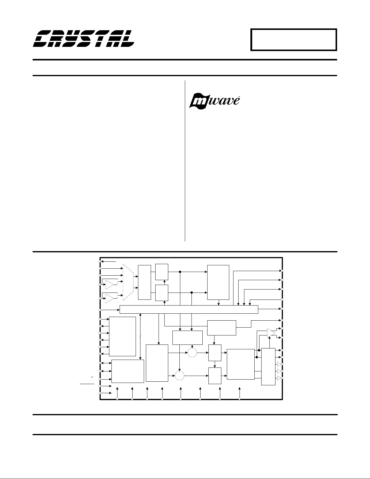
General Description
The CS4215 is an Mwave
audio codec.
The CS4215 is a single-chip, stereo, CMOS multimedia codec that supports CD-quality music,
FM radio-quality music, telephone-quality speech, and
modems. The analog-to-digital and digital-to-analog
converters are 64×oversampled delta-sigma converters
with on-chip filters which adapt to the sample frequency selected.
The +5V only power requirement makes the CS4215
ideal for use in workstations and personal computers.
Integration of microphone and line level inputs, input
and output gain setting, along with headphone and
monitor speaker driver, results in a v ery small footprint.
Ordering Information:
CS4215-KL 0°C to 70°C 44-pin PLCC
CS4215-KQ 0°C to 70°C 100-pin TQFP
CDB4215 Evaluation Board
TM
CMOUT
LINL
LINR
MINL
MINR
SDIN
CLKIN
CLKOUT
XTL1IN
XTL1OUT
XTL2IN
XTL2OUT
PIO0
PIO1
D/C
RESET
PDN
8
unsigned
decode
A/D
A/D
-law
µ
A-law
Serial Input/Output
Monitor
Attenuator
+
+
M
Gain
U
X
Clock
Generator
Control
Interface and
Registers
VA1 VA2 VD1 VD2 AGND1 AGND2 DGND1 DGND2
unsigned
-law
µ
A-law
encode
Voltage
Reference
D/A
D/A
Output
Attenuator
Mute
SDOUT
SCLK
FSYNC
TSIN
TSOUT
VREF
MOUT1
MOUT2
LOUTR
LOUTL
HEADC
HEADR
HEADL
This data sheet was written for Revision E CS4215 codecs and later. For differences between Revision E and
previous versions, see
Appendix A
.
Crystal Semiconductor Corporation
P.O. Box 17847, Austin, TX 78760
(512) 445-7222 FAX: (512) 445-7581
Copyright Crystal Semiconductor Corporation 1993
(All Rights Reserved)
SEPT ’93
DS76F2
1
CS4215
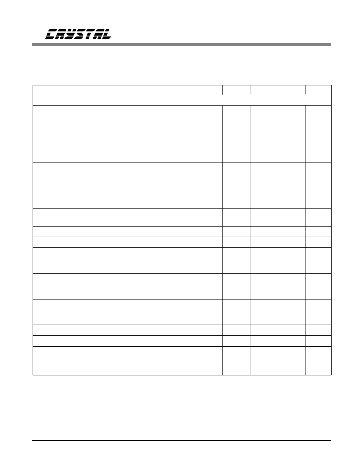
ANALOG CHARACTERISTICS( T
Input Levels: Logic 0 = 0V, Logic 1 = VD1, VD2; Full Scale Input Sine wave, No Gain, No Attenuation 1 kHz;
Conversion Rate = 48 kHz; No Gain, No Attenuation, SCLK = 3.072 MHz; Measurement Bandwidth is 10 Hz to
20 kHz; Slave mode; Unless otherwise specified.)
Parameter * Symbol Min Typ Max Units
Analog Input Characteristics
ADC Resolution 16 - - Bits
ADC Differential Nonlinearity - - ±0.9 LSB
Instantaneous Dynamic Range Line Inputs IDR 80 84 - dB
Total Harmonic Distortion Line Inputs THD - - 0.012 %
Interchannel Isolation Line to Line Inputs - 80 - dB
Interchannel Gain Mismatch Line Inputs - - 0.5 dB
Frequency Response (Note 1) (0 to 0.45 Fs) -0.5 - +0.2 dB
Programmable Input Gain Line Inputs -0.2 - 23.5 dB
- Minimum gain setting (0 dB); unless other wise specified.
= 25°C; VA1, VA2, VD1, VD2 = +5V;
A
Mic Inputs 72 78 - dB
Mic Inputs - - 0.032 %
Line to Mic Inputs - 60 - dB
Mic Inputs - - 0.5 dB
Mic Inputs 19.8 - 44 dB
Gain Step Size - 1.5 - dB
Absolute Gain Step Error - - 0.75 dB
Offset Error Line Inputs (AC Coupled) - ±150 ±400
with HPF = 0 Line Inputs (DC Coupled) - ±10 ±150 LSB
(No Gain) Mic Inputs - ±400 -
Offset Error Line Inputs (AC Coupled) - 0 ±5
with HPF = 1 (Notes 1,2) Line Inputs (DC Coupled) - 0 ±5LSB
(No Gain) Mic Inputs - 0 ±5
Full Scale Input Voltage: (MLB=0) Mic Inputs 0.250 0.28 0.310 Vpp
(MLB=1) Mic Inputs 2.50 2.8 3.10 V
Line Inputs 2.50 2.8 3.10 V
Gain Drift - 100 - ppm/°C
Input Resistance (Note 3) 20 - - kΩ
Input Capacitance - - 15 pF
CMOUT Output Voltage (Note 4) 1.9 2.1 2.3 V
(Maximum output current = 400 µA)
Notes: 1. This specification is guaranteed by characterization, not production tes ting.
2. Very low frequency signals will be slightly distorted when using the HPF.
3. Input resistance is for the input selec ted. Non-selected inputs have a very high (>1M Ω) input
resistance.
4. DC current only. If dynamic loading exists, then CMOUT must be buffered or the performance of
ADC’s and DAC’s may be degraded.
Parameter definitions are given at the end of this data sheet.
*
Mwave is a trademark of the IBM Corporation.
pp
pp
2 DS76F2
Specifications are subject to change without notice.
ANALOG CHARACTERISTICS (Continued)
Parameter * Symbol Min Typ Max Units
CS4215
Analog Output Characteristics
- Minimum Attenuation; Unless Otherwise Specified.
DAC Resolution 16 - - Bits
DAC Differential Nonlinearity - - ±0.9 LSB
Total Dynamic Range TDR - 95 - dB
Instantaneous Dynamic Range (OLB = 1) (All Outputs) IDR 80 85 - dB
Total Harmonic Distortion Line Out (Note 5) - - 0.025 %
(OLB = 1) Headphone Out (Note 6) THD - - 0.2 %
Speaker Out (Note 6) - - 0.32 %
Interchannel Isolation Line Out (Note 5) - 80 - dB
Headphone Out (Note 6) - 40 - dB
Interchannel Gain Mismatch Line Out - - 0.5 dB
Headphone - - 0.5 dB
Frequency Response (Note 1) (0 to 0.45 Fs) -0.5 - +0.2 dB
Programmable Attenuation (All Outputs) 0.2 - -94.7 dB
Attenuation Step Size - 1.5 - dB
Absolute Attenuation Step Error - - 0.75 dB
Offset Voltage Line Out - 10 - mV
Full Scale Output Voltage Line Output (Note 5) 2.55 2.8 3.08 V
with OLB = 0 Headphone Output (Note 6) 3.6 4.0 4.4 V
Speaker Output-Differential (Note 6) 7.3 8.0 8.8 V
Full Scale Output Voltage Line Output (Note 5) 1.8 2.0 2.2 V
with OLB = 1 Headphone Output (Note 6) 1.8 2.0 2.2 V
Speaker Output-Differential (Note 6) 3.6 4.0 4.4 V
pp
pp
pp
pp
pp
pp
Gain Drift - 100 - ppm/°C
Deviation from Linear Phase - - 1 Degree
Out of Band Energy (22 kHz to 100 kHz) Line Out - -60 - dB
Power Supply
Power Supply Current (Note 7) Operating - 110 140 mA
Power Down - 0.5 2 mA
Power Supply Rejection (1 kHz) - 40 - dB
Notes: 5. 10 kΩ, 100 pF load. Headphone and Speaker outputs disabled.
6. 48 Ω, 100 pF load. For the headphone outputs, THD with 10kΩ, 100pF load is 0.02%.
7. Typically, 50% of the power supply current is supplied to the analog power pins (VA1, VA2)
and 50% is supplied to the digital power pins (VD1, VD2). Values given are for unloaded outputs.
DS76F2 3
CS4215
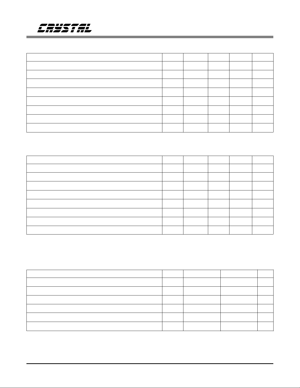
A/D Decimation Filter Characteristics
Parameter Symbol Min Typ Max Units
Passband (Fs is conversion freq.) 0 - 0.45Fs Hz
Frequency Response -0.5 - +0.2 dB
Passband Ripple - - ±0.1 dB
Transition Band 0.45Fs - 0.55Fs Hz
Stop Band ≥ 0.55Fs - - Hz
Stop Band Rejection 74 - - dB
Group Delay - 16/Fs - s
Group Delay Variation vs. Frequency - - 0.0 µs
D/A Interpolation Filter Characteristics
Parameter Symbol Min Typ Max Units
Passband (Fs is conversion freq.) 0 - 0.45Fs Hz
Frequency Response -0.5 - +0.2 dB
Passband Ripple - - ±0.1 dB
Transition Band 0.45Fs - 0.55Fs Hz
Stop Band ≥ 0.55Fs - - Hz
Stop Band Rejection 74 - - dB
Group Delay - 16/Fs - s
Group Delay Variation vs. Frequency - - 0.1/Fs s
DIGITAL CHARACTERISTICS (T
Parameter Symbol Min Max Units
High-level Input Voltage V
Low-level Input Voltage V
High-level Output Voltage at I0 = -2.0 mA V
Low-level Output Voltage at I0 = 2.0 mA V
Input Leakage Current (Digital Inputs) - 10 µA
= 25°C; VA1, VA2, VD1, VD2 = 5V)
A
(VD1,VD2)-1.0 (VD1,VD2)+0.3 V
IH
IL
OH
OL
-0.3 1.0 V
(VD1,VD2)-0.2 - V
-0.1V
Output Leakage Current (High-Z Digital Outputs) - 10 µA
4 DS76F2
CS4215
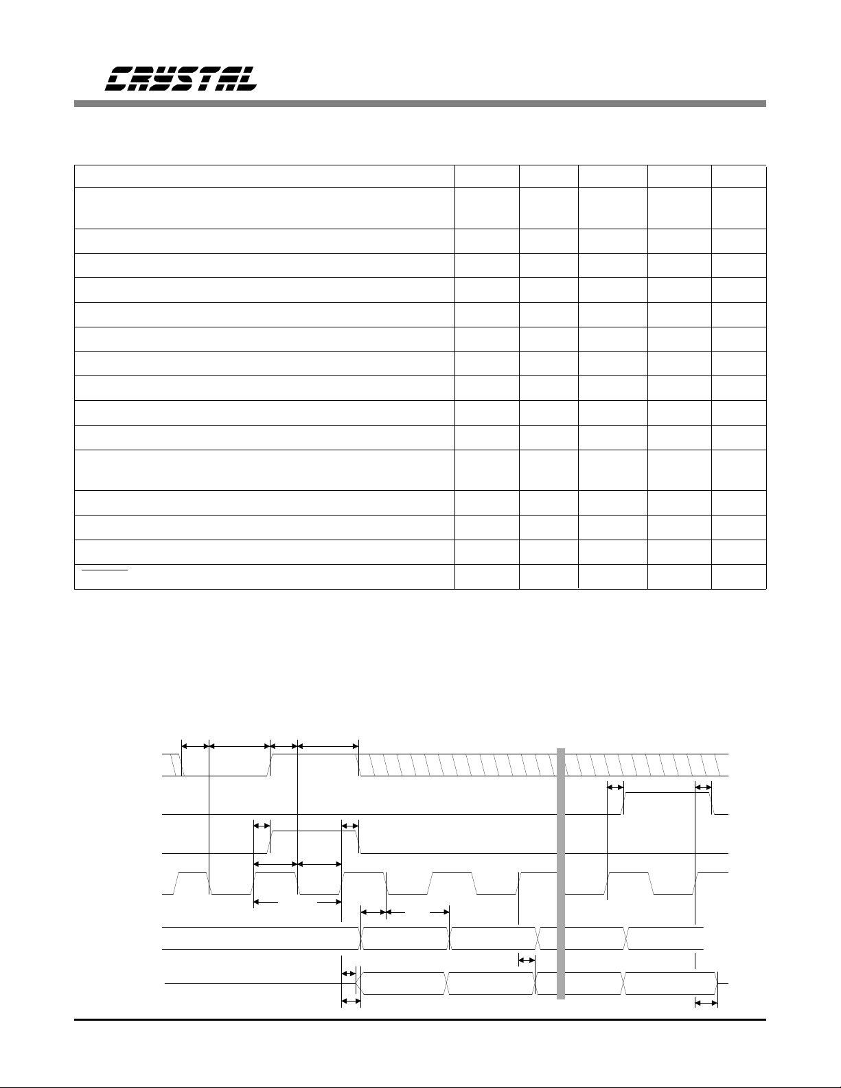
SWITCHING CHARACTERISTICS
(TA = 25°C; VA1, VA2, VD1, VD2 = +5V,
outputs loaded with 30 pF; Input Levels: Logic 0 = 0V, Logic 1 = VD1, VD2)
Parameter Symbol Min Typ Max Units
SCLK period Master Mode, XCLK = 1 (Note 8) t
sckw
-1/(Fs
bpf) - s
*
Slave Mode (XCLK = 0) tsckw 80 - - ns
SCLK high time Slave Mode, XCLK = 0 (Note 9) tsckh 25 - - ns
SCLK low time Slave Mode, XCLK = 0 (Note 9) tsckl 25 - - ns
Input Setup Time t
Input Hold Time t
s1
h1
15 - - ns
10 - - ns
Input Transition Time 10% to 90% points - - 10 ns
Output delay tpd1 - - 28 ns
SCLK to TSOUT tpd2 - - 30 ns
Output to Hi-Z state Timeslot 8, bit 0 t
Output to non-Hi-Z Timeslot 1, bit 7 t
hz
nz
- - 12 ns
15 - - ns
Input Clock Frequency Crystals - - 27 MHz
CLKIN (Note 10) 1.024 - 13.5 MHz
Input Clock (CLKIN) low time 30 - - ns
Input Clock (CLKIN) high time 30 - - ns
Sample rate Fs 4 - 50 kHz
RESET low time (Note 11) 500 - - ns
Notes: 8. In Master mode with BSEL1,0 set to 64 or 128 bits per frame (bpf), the SCLK duty cycle is 50%.
When BSEL1,0 is set to 256 bpf, SCLK will have the same duty cycle as CLKOUT.
See Internal Clock Generation section.
9. In Slave mode, FSYNC and SCLK must be derived fr om the master clock running the codec
(CLKIN, XTAL1, XTAL2).
10. Sample rate specifications must not be exceeded.
11. After powering up the CS 4215, RESET should be held low for 50 ms to allow the v oltage
reference to settle.
FSYNC
TSIN
TSOUT
FSYNC
SCLK
SDIN
SDOUT
t
in
out
s1
t
t
t
pd1
sckh
h1
t
s1
t
sckw
t
t
h1
t
nz
pd1
t
pd1
t
sckl
t
s1
t
h1
TS 1, Bit 7
TS 1, Bit 7 TS 1, Bit 6
t pd1
t
pd2
TS 8, Bit 0TS 1, Bit 6
TS 8, Bit 0
t
t
pd2
hz
DS76F2 5
CS4215
ABSOLUTE MAXIMUM RATINGS (AGND, DGND = 0V, all voltages with respect to 0V.)
Parameter Symbol Min Max Units
Power Supplies: Digital VD1,VD2 -0.3 6.0 V
Analog VA1,VA2 -0.3 6.0 V
Input Current (Except Supply Pins) - ±10.0 mA
Analog Input Voltage -0.3 (VA1, VA 2)+0.3 V
Digital Input Voltage -0.3 (VD1, VD2)+0.3 V
Ambient Temperature (Power Applied) -55 +125 °C
Storage Temperature -65 +150 °C
Warning: Operation bey ond these limits may result in per manent damage to the device.
Normal operation is not guaranteed at these extremes.
RECOMMENDED OPERATING CONDITIONS (AGND, DGND = 0V, all voltages with re-
spect to 0V.)
Parameter Symbol Min Typ Max Units
Power Supplies: Digital (Note 8) VD1,VD2 4.75 5.0 5.25 V
Analog (Note 8) VA1,VA2 4.75 5.0 5.25 V
Operating Ambient Temperature T
Note: 8. VD - VA must be less than 0.5 V olts (one diode drop).
A
02570°C
6 DS76F2
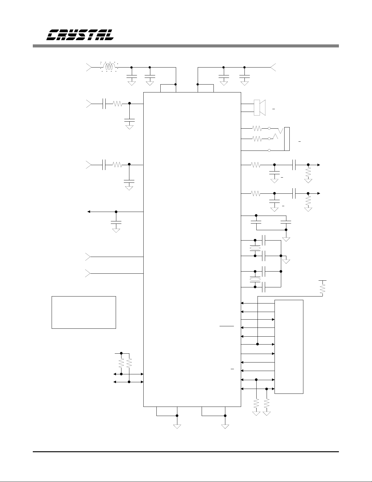
+5V Digital
Supply
Ferrite Bead
1 uF
CS4215
+5V Analog
+
0.1 uF
0.1 uF
+
1 uF
Supply
Microphone
Input Right
Microphone
Input Left
To O ptio nal
Input Buffers
0.47 uF
See Line Level
Inp uts S e ction
Refer to the
section for terminating
unused line and mic inputs.
All other unused inputs
should be tied to GND. All NC
pins should be left floating.
Analog Inputs
0.47 uF
0.01 uF
0.47 uF
0.01 uF
VD1
47k
150
NPO
150
NPO
15
17
19
16
18
36
37
MINR
MINL
CMOUT
LINR
LINL
PIO0
PIO1
38
CS4215
2324
VA1VA2VD1 VD2
MOUT1
MOUT2
HEADR
HEADL
HEADC
LOUTR
LOUTL
VREF
XTL2IN
XTL2O UT
XTL1IN
XTL1O UT
SDIN
CLKIN
CLKOUT
RESET
PDN
SDOUT
TSOUT
TSIN
D/C
SCLK
FSYNC
28
27
12
Ω
29
31
12
Ω
30
600
Ω
33
0.0022 uF
NPO
600
Ω
32
0.0022 uF
NPO
21
10
11
6
7
1
4
5
12
13
44
41
40
35
43
42
1/2W
1/2W
0.1 uF
40pF
40pF
40pF
40pF
32
>
Ω
Headphone
> 1.0 uF
>
16.9344 MHz
24.576 MHz
Controller
Jack
+
+
1.0 uF
+
10 uF
>48
Ω
40 k
40 k
+5v
20k
AGND1 AGND2 DGND1 DG ND2
22 2 5 2 9
20k 20k
Note: AGND and DGND pins must be on the same ground plane.
Figure 1. Recommended Connection Diagram
DS76F2 7
CS4215
FUNCTIONAL DESCRIPTION
Overview
The CS4215 has two channels of 16-bit analogto-digital conversion and two channels of 16-bit
digital-to-analog conversion. Both the ADCs and
the DACs are delta-sigma converters. The ADC
inputs have adjustable input gain, while the DAC
outputs have adjustable output attenuation. Special features include a separate microphone input
with a 20 dB programmable gain block, an op-
tional 8-bit µ-law or A-law encoder/decoder, pins
for two crystals to set alternative sample rates,
direct headphone drive and mono speaker drive.
Control for the functions available on the
CS4215, as well as the audio data, are communicated to the device over a serial interface.
Separate pins for input and output data are provided, allowing concurrent writing to and
reading from the device. Data must be continually written for proper operation. Multiple
CS4215 devices may be attached to the same
data lines.
Analog Inputs
Unused analog inputs that are not selected have
a very high input impedance, so they may be
tied to AGND directly. Unused analog inputs
that are selected should be tied to AGND
through a 0.1uF capacitor. This prevents any DC
current flow.
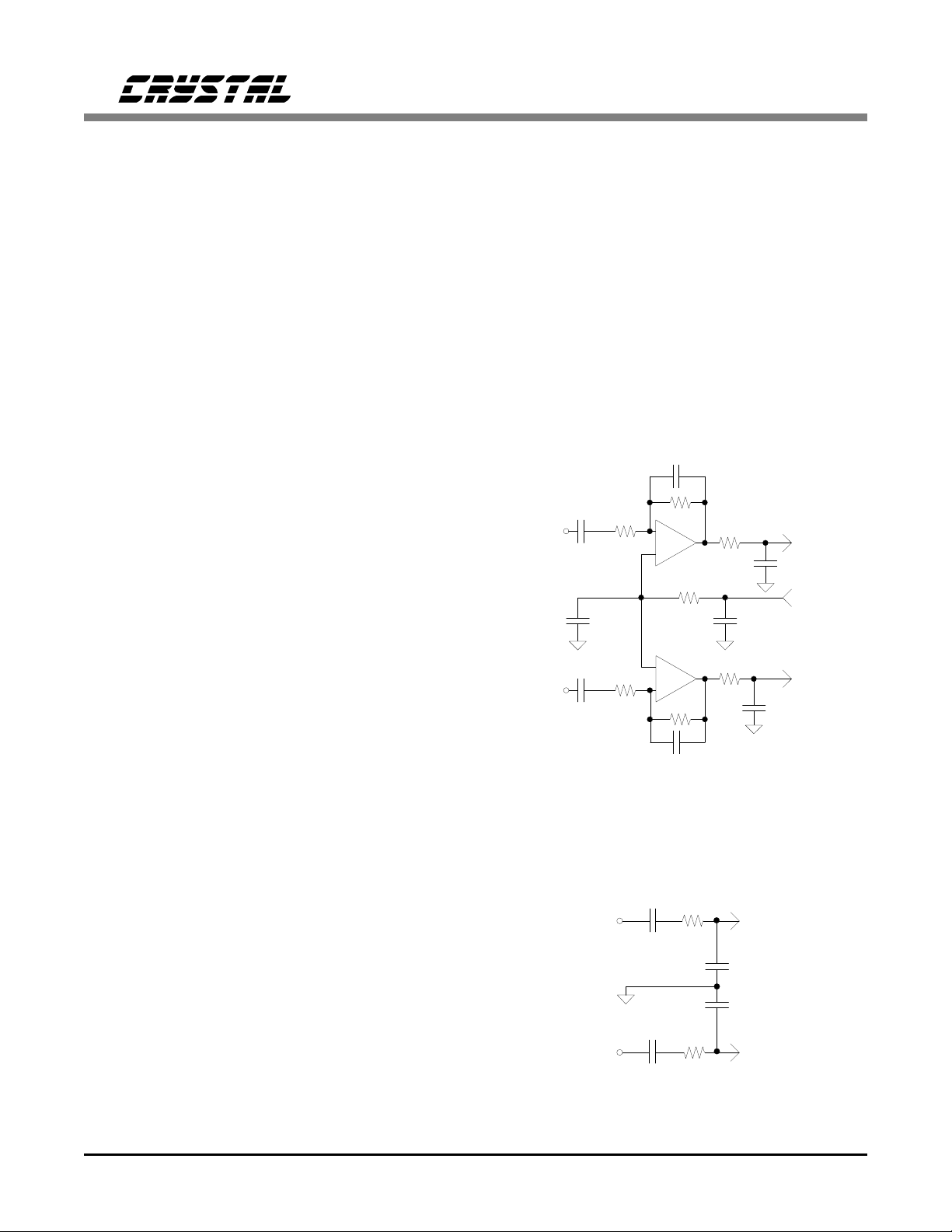
Line Level Inputs
LINL and LINR are the line level input pins.
These pins are internally biased to the CMOUT
voltage. Figure 2 shows a dual op-amp buffer
which combines level shifting with a gain of 0.5
to attenuate the standard line level of 2 V
56 pF
Line In
Right
Example
Op-Amps
are
LT1013
Line In
Left
0.47 uF
0.47 uF
20 k
0.47 uF
20 k
10 k
_
+
+
_
5 k
10 k
150
0.01 uF
NPO
150
(pin 16)
0.47 uF
0.01 uF
NPO
rms
LINR
CMOUT
(pin 19)
LINL
(pin 18)
to
Figure 1, the recommended connection diagram,
shows examples of the external analog circuitry
recommended around the CS4215. An internal
multiplexer selects between line level inputs and
microphone level inputs.
Op-amps are run
from VA1, VA2 and
AGND.
Figure 2. DC Coupled Input.
56 pF
Input filters using a 150 Ω resistor and a .01 µF
NPO capacitor to ground are required to isolate
the input op-amps from, and provide a charge re-
Line In
Right
serve for, the switched-capacitor input of the
codec. The RC values may be safely changed
by a factor of two.
The HPF bit in Control Time Slot 2 provides a
high pass filter that will reduce DC offset on the
Line In
Left
analog inputs. Using the high pass filter will
cause slight distortions at very low frequencies.
8 DS76F2
Figure 3. AC Coupled Input.
0.47 uF
0.47 uF
150
150
LINR
(pin 16)
0.01 uF
NPO
NPO
0.01 uF
LINL
(pin 18)
CS4215
MINR
MINL
(Mono)
10 uF
10 uF
R6
2.2 k
+
C6
1 uF
+
C5
C2
+
1 uF
2.2 k
R3
+
C3
R4
22.1 k
VA+
2
3
R5
50 k
R2
50 k
5
6
C1 560 pF
C4
560 pF
NPO
C8
8
0.1 uF
1
4
U2
MC33078 or
MC33178
C7
7
A =20 dB
NPO
22.1 k
R1
C48
0.47 uF
+
1 uF
0.47 uF
C45
R56
150
C47
R57
150
C46
Microphone
Input Right
(pin 15)
NPO
0.01 uF
CMOUT
Microphone
Input Left
(pin 17)
NPO
0.01 uF
Figure 4. Optional Microphone Input Buffer
1 V
. The CMOUT reference level is used to
rms
level shift the signal. This level shifting allows
the line inputs to be DC coupled into the
CS4215. Minimum ADC offset results when the
line inputs are DC coupled (see Analog Characteristics Table).
Figure 3 shows an AC coupled input circuit for
signals centered around 0 Volts. The anti-aliasing RC filter presents a low impedance at high
frequencies and should be driven by a low impedance source.
Microphone Level Inputs
Internal amplifiers with a programmable 20 dB
gain block are provided for the microphone level
inputs, MINR and MINL. Figure 4 shows a single-ended input microphone pre-amplifier stage
with a gain of 23 dB. AC coupling is mandatory
for these inputs since any DC offset on the input
will be amplified by the codec.
The 20 dB gain block may be disabled using the
MLB bit in Control Time Slot 1. When disabled, the inputs become line level with full
scale inputs of 1 Vrms.
Adjustable Input Gain
The signals from the microphone or the line inputs are routed to a programmable gain circuit
which provides up to 22.5 dB of gain in 1.5 dB
steps. Level changes only take effect on zero
crossings to minimize audible artifacts, often referred to as "zipper noise". The requested level
change is forced if no zero crossing is found after 511 frames (10.6 ms at a 48 kHz frame rate).
A separate zero crossing detector exists for each
channel.
Analog Outputs
The analog outputs of the DACs are routed via
an attenuator to a pair of line outputs, a pair of
DS76F2 9

CS4215
headphone outputs and a mono monitor speaker
output.
Output Level Attenuator
The DAC outputs are routed through an attenuator, which provides 0 dB to 94.5 dB of
attenuation, adjustable in 1.5 dB steps. Level
changes are implemented using both analog and
digital attenuation techniques. Level changes
only take effect on zero crossings to minimize
audible artifacts. The requested level change is
forced if an analog zero crossing does not occur
within 511 frames (10.6 ms at a 48 kHz frame
rate). A separate zero crossing detector exists for
each channel.
Line Outputs
LOUTR and LOUTL output an analog signal,
centered around the CMOUT voltage. The mini-
mum recommended load impedance is 8 kΩ.
Figure 1 shows the recommended 1.0 µF DC
blocking capacitor with a 40 kΩ resistor to
ground. When driving impedances greater than
10 kΩ, this provides a high pass corner of
20 Hz. These outputs may be muted.
Headphone Outputs
HEADR and HEADL output an analog signal,
centered around the HEADC voltage. The default headphone output level (OLB = 0) contains
an optional 3 dB gain over the line outputs
which provides reasonable listening levels, even
with small amplitude digital sources. These outputs have increased current drive capability and
can drive a load impedance as low as 48 Ω. External 12 Ω series resistors reduce output level
variations with different impedance headphones.
The common return line from driving headphones should be connected to HEADC, which
is biased to the CMOUT voltage. This removes
the need for AC coupling, and also controls
where the return currents flow. All three head-
phone output lines are short-circuit protected.
These outputs may be muted.
Speaker Output
MOUT1 and MOUT2 differentially drive a small
loudspeaker, whose impedance should be greater
than 32 Ω. The signal is a summed version of
the right and left line output, tapped off prior to
the mute function, but after the attenuator. The
speaker output may be independently muted.
With OLB = 0, the speaker output also contains
a 3 dB gain over the line outputs. When
OLB = 1, the speaker outputs are driven at the
same level as the line outputs.
Some small speakers distort heavily when presented with low frequency energy. A high-pass
filter helps eliminate the low frequency energy
and can be implemented by AC coupling both
speaker terminals with a resistor to ground, on
the speaker side of the DC blocking capacitors.
The values selected would depend on the speaker
chosen, but typical values would be 22 µF for
the capacitors, with the positive side connected
to the codec, and 50 kΩ resistors. T his circuit is
contained on the CDB4215 evaluation board as
shown in the end of this data sheet.
Input Monitor Function
To allow monitoring of the input audio signal,
the output of the ADCs can be routed through a
monitor path attenuator, then digitally mixed into
the input data for the DACs (see the front page
block diagram). Changes in the input gain or
output level settings directly affect the monitor
level. If full scale data from the ADCs is added
to full scale digital data from the serial in terface,
clipping will occur.
Calibration
Both output offset voltage and input offset error
are minimized by an internal calibration cycle.
At least one calibration cycle must be invoked
10 DS76F2
FSYNC
SCLK
CLKOUT
8.5 CLKOUT's
11 CLKOUT's
Data Mode -Read and Write
TSIN
SCLK
1 SCLK
Control Mode - Read Only
CS4215
PIO Read
PIO Write
PIO Read
Notes:
DATA MODE READ - The data is sent out via SDOUT on the next frame.
1.
2.
CONTROL MODE READ - The data is sent out, via SDOUT, the same frame.
3.
DATA MODE READ, WRITE - are tied to the rising edge of FSYNC and CLKOUT.
They are independent of SCLK.
4.
CONTROL MODE READ - The PIO pins are sampled by a rising edge of SCLK.
Figure 5. PIO Pin Timing
after power up. A calibration cycle will occur
immediately after leaving the reset state. A calibration cycle will also occur immediately after
going from control mode to data mode (D/C going high). When powering up the CS4215, or
exiting the power down state, a minimum of
50 ms must occur, to allow the voltage reference
to settle, before initiating a calibration cycle.
This is achieved by holding RESET low or staying in control mode for 50 ms after power up or
exiting power down mode. The input offset error
will be calibrated for whichever input channel is
selected (microphone or line, using the IS bit).
Therefore, the IS bit should remain steady while
the codec is calibrating, although the other bits
input to the codec are ignored. Calibration takes
194 FSYNC cycles and SDOUT data bits will be
zero during this period. The A/D Invalid bit, ADI
(bit 7 in data time slot 6), will be high during
calibration and will go low when calibration is
finished.
Parallel Input/Output
Two pins are provided for parallel input/output.
These pins are open drain outputs and require
external pull-up resistors. Writing a zero turns on
the output transistor, pulling the pin to ground;
writing a one turns off the output transistor,
which allows an external resistor to pull the pin
high. When used as an input, a one must be written to the pin, thereby allowing an external
device to pull it low or leave it high. These pins
can be read in control mode and their state is
recorded in Control Register 5. These pins can
be written to and read back in data mode using
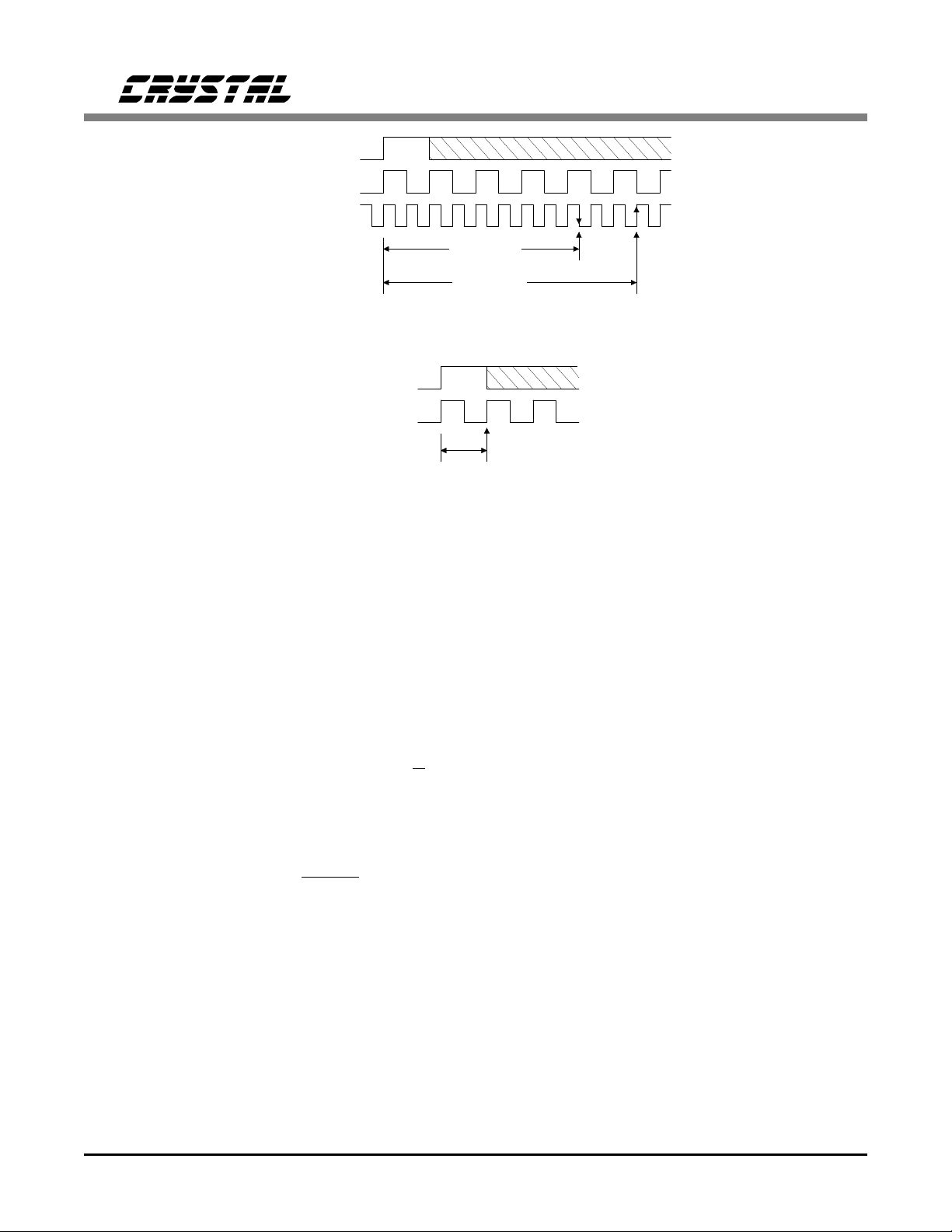
Data Register 7. Figure 5 shows the Parallel Input/Output timing.
DS76F2 11
CS4215
Clock Generation
The master clock operating the CS4215 may be
generated using the on-chip crystal oscillators, or
by using an external clock source. In all data
modes SCLK and FSYNC must be synchronous
to the selected master clock.
If the master clock source stops, the digital filters will power down after 5 µs to prevent
overheating. If FSYNC stops, the digital filters
will power down after approximately 1 FSYNC
period. The CS4215 will not enter the total
power down state.
Internal Clock Generation
Two external crystals may be attached to the
XTL1IN, XTL1OUT, XTL2IN and XTL2OUT
pins. Use of an external crystal requires additional 40 pF loading capacitors to digital ground
(see Figure 1). XTAL1 oscillator is intended for
use at 24.576 MHz and XTAL2 oscillator is intended for use at 16.9344 MHz, although other
frequencies may be used. The gain of the internal inverter is slightly higher for XTAL1,
ensuring proper operation at >24 MHz frequencies. The crystals should be parallel resonant,
fundamental mode and designed for 20 pF loading (equivalent to a 40 pF capacitor on each leg).
If XTAL1 or XTAL2 is not selected as the master clock, that particular crystal oscillator is
powered down to minimize interference. If a
crystal is not needed, the XTL-IN pin should be
grounded. An example crystal supplier is CAL
Crystal, telephone number (714) 991-1580.
FSYNC and SCLK must be synchronous to the
master clock. When using the codec in slave
mode with one of the crystals as master clock,
the controller must derive FSYNC and SCLK
from the crystals, i.e. via CLKOUT. Note that
CLKOUT will stop in a low condition within
two periods after D/C goes low.
An internally generated clock which is 256 times
the sample rate (FSYNC rate) is output
(CLKOUT) for potential use with an external
AES/EBU transmitter, or another CS4215. No
glitch occurs on CLKOUT when selecting alternate clock sources. CLKOUT will stop in a low
condition within two periods after D/C goes low,
assuming one of the crystal oscillators is selected, or either CLKIN or SCLK is the master
clock source and is continuous. The duty cycle
of CLKOUT is 50% if the master clock is one of
the crystal oscillators and the DFR bits are 0, 1,
2, 6 or 7. If the DFR bits are 3 or 5, the duty
cycle is 33% (high time). If the DFR bits are 4
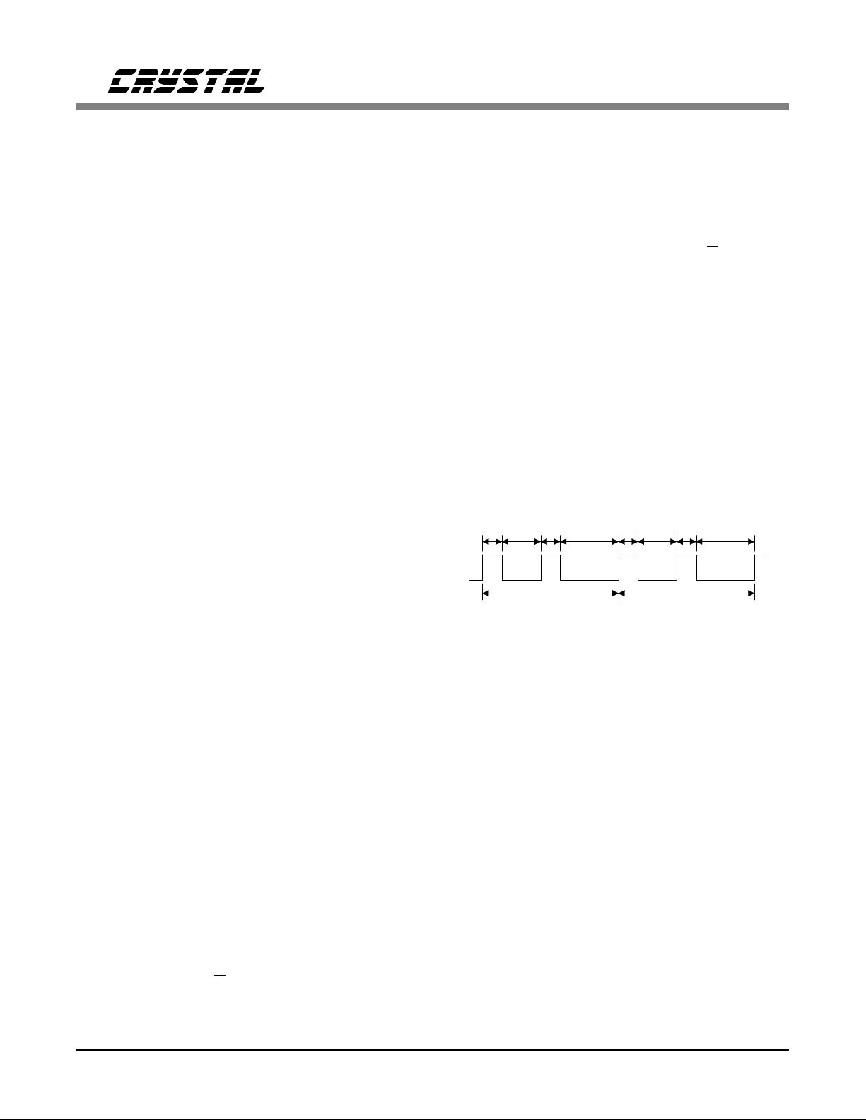
then CLKOUT has the timing shown in Figure 6.
If the master clock is SCLK or CLKIN, the duty
cycle of CLKOUT will be the same as the master clock source.
1213
1/(128 x FSYNC) 1/(128 x FSYNC)
Figure 6. CLKOUT duty cycle using the on-chi p
crystal oscillator when DFR = 4
( typically FSYNC = 37.8 kHz)
1213
External Clock
An external clock input pin (CLKIN) is provided
for potential use with an external AES/EBU receiver, or an already existing system clock.
When MCK2 = 0, the input clock must be exactly 256 times the sample rate, and FSYNC and
SCLK must be synchronous to CLKIN. When
MCK2 = 1 the DFR bits allow various divide
ratios off the CLKIN frequency.
Alternatively, an external high frequency clock
may be driven into XTL1IN or XTL2IN. The
correct clock source must be selected using the
MCK bits. Manipulating DFR bits will allow
various divide ratios from the clock to be se-
12 DS76F2
CS4215
lected. SCLK and FSYNC must be synchronous
to the external clock.
As a third alternative, SCLK may be programmed to be the master clock input. In this
case, it must be 256 times Fs.
Serial Interface
The serial interface of the CS4215 transfers digital audio data and control data into and out of
the device. Multiple CS4215 devices may share
the same data lines. DSP’s supported include the
Motorola 56001 in network mode and a subset
of the ‘CHI’ bus from AT&T/Intel.
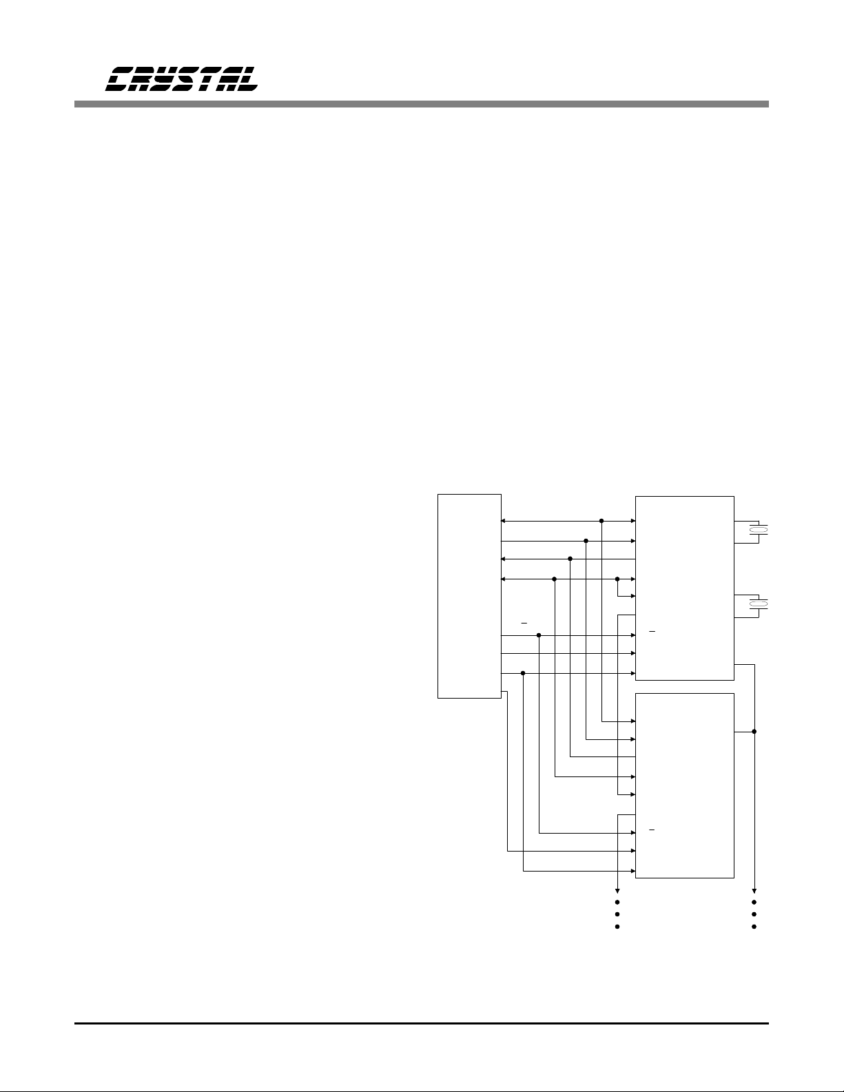
Serial Interface Signals
Figure 7 shows an example of two CS4215 devices connected to a common controller. The
Serial Data Out (SDOUT) and Serial Data In
(SDIN) lines are time division multiplexed between the CS4215s.
The serial interface clock, SCLK, is used for
transmitting and receiving data. SCLK can be
generated by one of the CS4215s, or it can be
input from an external SCLK source. When generated by an external source, SCLK must be
synchronous to the master clock. Data is transmitted on the rising edge of SCLK and is
received on the falling edge of SCLK. The
SCLK frequency is always equal to the bit rate.
The Frame Synchronizing signal (FSYNC) is
used to indicate the start of a frame. It may be
output from one of the CS4215s, or it may be
generated from an external controller. If FSYNC
is generated externally, it must be high for at
least 1 SCLK period, and it must fall at least
2 SCLKs before the start of a new frame (see
Figure 8). It must also be synchronous to the
master clock. The frequency of FSYNC is equal
to the system sample rate (see Figure 8). Each
CS4215 requires 64 SCLKs to transfer all the
data. The SCLK frequency can be set to 64, 128,
or 256 bits per frame, thereby allowing for 1, 2
or 4 CS4215s connected to the same bus.
In a typical multi-part scenario, one CS4215 (the
master) would generate FSYNC and SCLK,
while the other CS4215s (the slaves) would receive FSYNC and SCLK. The CLKOUT of the
master would be connected to the CLKIN of
each slave device as shown in Figure 7. Then,
the master device would be programmed for the
desired sample frequency (assuming one of the
crystals is selected as the clock source), the number of bits per frame, and for SCLK and FSYNC
to be outputs. The slave devices would be programmed to use CLKIN as the clock source, the
same number of bits per frame, and for SCLK
and FSYNC to be inputs. Since CLKOUT is al-
SCLK
SDIN
SDOUT
FSYNC
TSIN
TSOUT
D/C
PDN
RESET
SCLK
SDIN
SDOUT
FSYNC
TSIN
TSOUT
D/C
PDN
RESET
CS4215
XTL1IN
XTL1OUT
A
XTL2IN
XTL2OUT
Master
CLKOUT
CS4215
CLKIN
B
Slave
Controller
SCLK
SDIN
SDOUT
FSYNC
D/C
Figure 7. Multiple CS4215’s
DS76F2 13
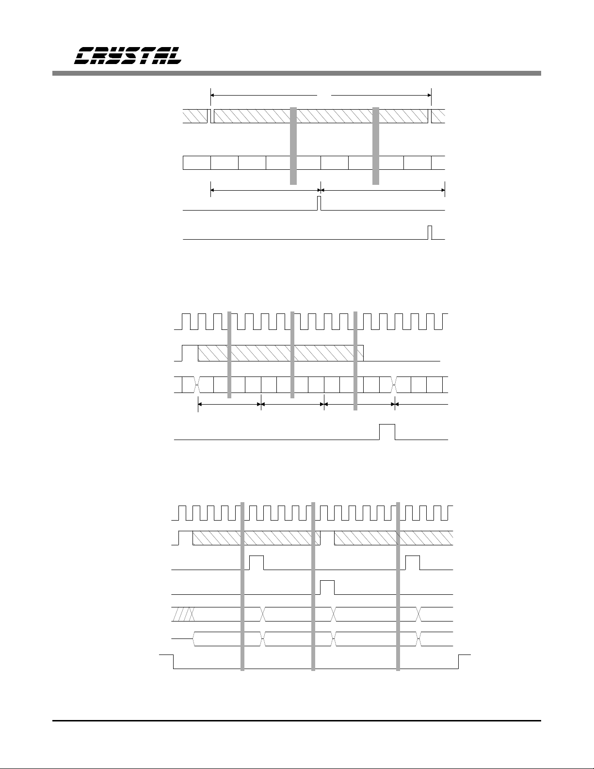
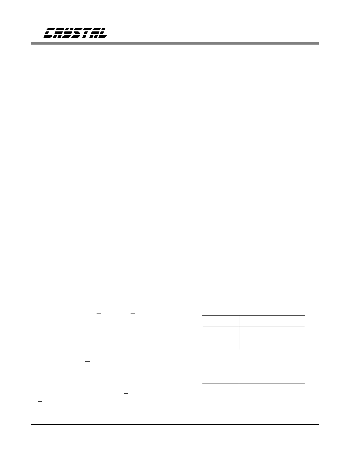
FSYNC
TSINA
CS4215
T1
TSn
TSOUTA
TSINB
TSOUTB
SCLK
FSYNC
TSIN
DATA
TSOUT
TS8
TS1 TS2 TS3 TS2 TS7 TS8
TS8 TS1
DEVICE BDEVICE A
T1 1/Frame Rate or 1/System Sample Rate
TSn Time slot numbers
Figure 8. Seria l Interface Timing for 2 CS42 15’s
1 2 8 9 16 17 18 64 65 66 67
70 70
TS1 TS2
10
7610 6576 1
6 1
0
TS3 TS8
TS1
68
Figure 9. Frame Sync and Bit Offset Timing
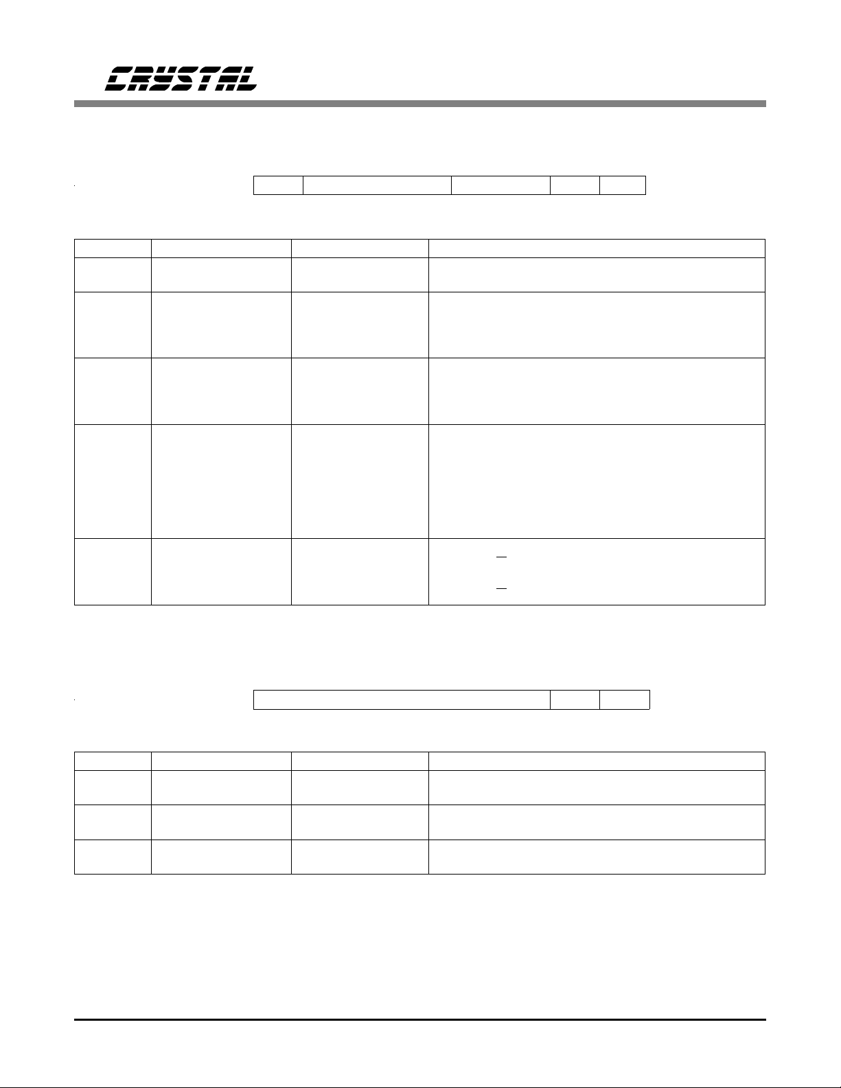
1 2 64 128 2 65 6665 66 1 64
SCLK
FSYNC,
TSIN A
TSOUT A,
TSIN B
TSOUT B
SDIN
SDOUT
D/C
3 4 67 68 3 4
Control to A Control to B
_
Control Mode
Control to A
Control from A Control from B
5
Figure 10. Control Mode Timing for 2 CS4215’s
14 DS76F2
CS4215
ways 256 times the sample frequency and scales
with the selected sample frequency on the master, the slave devices will automatically scale
with changes in the master codec’s sample frequency.
CS4215s are time division multiplexed onto the
bus using the Time Slot Out (TSOUT) and Time
Slot In (TSIN) signals. TSOUT is an output signal that is high for one SCLK bit time, and
indicates that the CS4215 is about to release the
bus. TSIN is an input signal that informs the
CS4215 that the next time slot is available for it
to use. The first device in the chain uses FSYNC
as its TSIN signal. All subsequent devices use
the TSOUT of the previous device as its TSIN
input. TSIN must be high for at least 1 SCLK
period and fall at least 2 SCLKs before start of a
new frame.
Serial Interface Operation
The serial interface format has a variable number
of time slots, depending on the number of
CS4215s attached to the bus. All time slots have
8 bits. Each CS4215 requires 8 time slots (64
bits) to communicate all data (see Figure 9).
CONTROL MODE
The Control Mode is used to set up the CS4215
for subsequent operation in Data Mode by loading the internal control registers. Control mode is
asserted by bringing D/C low. If D/C is low during power up, then the CS4215 will enter control
mode immediately. The SCLK and FSYNC pins
are tri-stated, and the CS4215 will receive SCLK
and FSYNC from an external source. If the
CS4215 is in master mode (SCLK and FSYNC
are outputs) and D/C is brought low, then SCLK
& FSYNC will continue to be driven for a minimum of 4 and a maximum of 12 SCLKs, if the
ITS bit = 0. If ITS is 1, SCLK and FSYNC will
three-state immediately after D/C goes low. If
D/C is brought low when the codec is programmed as master with ITS=0, the codec will
timeout and release FSYNC and SCLK within
100µs. The values in the control registers for
control of the serial ports are ignored in control
mode. The data received on SDIN is stored into
the control registers which have addresses
matching their time slots. The data in the registers is transmitted on SDOUT with the time slot
equal to the register number (see Figure 10).
The steps involved when going from data mode
to control mode and back are shown in the flow
chart in Figure 11.
Control Formats
The CS4215 control registers have the functions
and time slot assignments shown in Table 1. The
register address is the time slot number when
D/C is 0. Reserved bits should be written as 0
and could be read back as 0 or 1. When comparing data read back, reserved bits should be
masked. The SDOUT pin goes into a
high-impedance state prior to Time Slot 1 and
after Time Slot 8. The data listed below the register is its reset state.
The parallel port register is used to read and
write the two open-drain input/output pins. The
outputs are all set to 1 on RESET. PIO bits are
read only in control mode. Note that, since PIO
signals are open drain signals, an external device
Time slot Description
1 Status
2 Data Format
3 Serial Port Control
4Test
5 Parallel Port
6 RESERVED
7 Revision
8 RESERVED
Table 1. Co ntrol Registers
DS76F2 15

may drive them low even when they have been
programmed as highs. Therefore, the value read
back may differ from the value written. In the
data mode, (D/C=1), this register can be read
and written to through the serial port as part of
the Input Settings Registers. In control mode,
(D/C=0) these bits can only be read.
CS4215
16 DS76F2

Lower output level to
maximum attenuation
Mute the speaker output
Set D/C low
CS4215
Wait at least 12 SCLK
periods for FSYNC and
SCLK to three-state
Set external controller to
receive SCLK and FSYNC
from the codec
Y
Read back and verify control information.
Y
Codec programmed for
Master mode & ITS=0?
N
Set external controller to
drive SCLK and FSYNC
into the codec
Poll for CLB=0?
Send valid control information
with CLB=0
Mask off reserved bits
CLB=0?
YY
Set CLB=1 and send at least
two more frames of valid
control information
Is codec
programmed for
Master mode?
1
Y
2
1
This is a software design choice,
not a run-time conditional branch.
N
Send valid control information
2
This will cause the codec to
ignore any further bus activity.
The SDOUT pin will be held in
the high impedance state after
transmitting 1 frame with CLB=1
n = 5
with CLB=0
n = n - 1
n = 0?
NN
N
Set D/C high.
Transmit/receive data with attenuated outputs
and muted speaker for 194 FSYNC cycles
while codec executes offset calibration
Transmit/receive audio data
with desired level settings
Figure 11. Control Mode Flow Cha rt
DS76F2 17

Control Time Slot 1, Status Register
D7 D6 D5 D4 D3 D2 D1 D0
Register
Reset (R)
BIT NAME VALUE FUNCTION
RSRV Reserved Bits Must be written as 0.
CLB Control Latch Bit 1
OLB Output Level Bit 0
MLB Microphone Level 0
001MLBOLBCLBRSRV
001001XX
R
Ensures proper transition between control and
data mode.
R
Line full scale outputs are 2.8 Vpp (1Vrms)
Headphone full scale output is 4.0 Vpp.
Speaker full scale output is 8.0 Vpp.
1
1
Line and Headphone full scale outputs are
2.0 Vpp. Speaker full scale output is 4.0 Vpp.
R
20 dB Fixed Gain Enabled
Full scale microphone inputs are 0.288 Vpp.
20 dB Fixed Gain Disabled
Full scale inputs are 2.88 Vpp.
CS4215
Control Time Slot 2, Data Format Register
D7 D6 D5 D4 D3 D2 D1 D0
Register
Reset (R)
BIT NAME VALUE FUNCTION
DF1-0 Data Format
Selection
ST Stereo B it 0
DFR2-0 Data Conversion
Frequency Selection
RSRV Reserved Bit Must be written as 0
HPF High Pass Filter 0
HPF RS RV DFR2 DFR1 DFR0 ST DF1 DF0
0X000001
0 0
0 1
1 0
1 1
1
0 0 0
0 0 1
0 1 0
0 1 1
1 0 0
1 0 1
1 1 0
1 1 1
1
0
1
2
3
0
1
2
3
4
5
6
7
16-bit 2
R
8-bit µ−Law.
8-bit A-Law.
8-bit unsigned linear.
R
Mono Mode.
Stereo Mode.
R
R
Disabled.
Enabled. A Digital High Pass Filter is used to force
’s
-complement linear.
CLKIN (
the ADC DC offset to zero.
÷)
3072 8 5.5125
1536 16 11.025
896 27.42857 18.9
768 32 22.05
448 NA 37.8
384 NA 44.1
512 48 33.075
2560 9.6 6.615
XTAL1(kHz) XTAL2 (kHz)
24.576 MHz 16.9344 MHz
18 DS76F2
Control Time Slot 3, Serial Port Control Register
D7 D6 D5 D4 D3 D2 D1 D0
Register
Reset (R)
BIT NAME VALUE FUNCTION
XEN Transmitter Enable 0
XCLK Transmit Clock 0
BSEL1-0 Select Bit Rate 0 0
MCK2-0 Clock Source Select 0 0 0
ITS Immediate Three-
State
ITS MCK2 MCK1 MCK0 BSEL1 BSEL0 XCLK X EN
00001001
Enable the serial data output.
1
1
0 1
1 0
1 1
0 0 1
0 1 0
0 1 1
1 0 0
0
1
R
Disable (high-impedance state) serial data output.
R
Receive SCLK and FSYNC from external source
SLAVE Mode
Generate SCLK and FSYNC
MASTER Mode
0
1
2
3
0
1
2
3
4
64 bits per frame.
128 bits per frame.
R
256 bits per frame.
Reserved.
R
SCLK is master clock, 256 bits per frame.
BSEL must equal 2, and XCLK must equal 0.
XTAL1, 24.576 MHz, is clock source.
XTAL2, 16.9344 MHz, is clock source.
CLKIN is clock source, and must be 256xFs.
CLKIN is clock source, DFR2-0 select sample
frequency.
R
SCLK and FSYNC three-state up to 12 clocks
after D/
SCLK and FSYNC three-state immediately
after D/
C goes low.
C goes low.
CS4215
Control Time Slot 4, Test Register
D7 D6 D5 D4 D3 D2 D1 D0
Register
Reset (R)
BIT NAME VALUE FUNCTION
DAD Loopback Mode 0
ENL Enable Loopback
Testing
TEST Test bits The TEST bits must be written as zero, otherwise
DS76F2 19
00000000
1
0
1
TEST ENL DAD
R
Digital-Digital Loopback.
Digital-Analog-Digital Loopback.
R
Disable.
Enable.
special factory test modes may be invoked.

Control Time Slot 5, Parallel Port Register
D7 D6 D5 D4 D3 D2 D1 D0
Register
Reset (R)
BIT NAME VALUE FUNCTION
RSRV Reserved Bits Must be written as 0.
PIO1-0 Parallel I/O Bits 1 1 3
PIO1 PIO0 RSRV
11XXXXXX
R
See the Parallel Input/Output Section.
Control Time Slot 6, Reserved Register
D7 D6 D5 D4 D3 D2 D1 D0
Register
Reset (R)
XXXXXXXX
RSRV
CS4215
BIT NAME VALUE FUNCTION
RSRV Reserved Bits Must be written as 0.
Control Time Slot 7, Ve rsion Register
D7 D6 D5 D4 D3 D2 D1 D0
Register
Reset (R)
BIT NAME VALUE FUNCTION
VER3-0 Device Version
Number
RSRV Reserved Bits Must be written as 0.
XXXX0010
RSRV VER3 VER2 VER1 VER0
0 0 0 0
0 0 0 1
0 0 1 0
0
1
2
"C". See
"D". See
R
"E". This Data Sheet
Appendix A.
Appendix A.
Control Time Slot 8, Reserved Register
D7 D6 D5 D4 D3 D2 D1 D0
Register
Reset (R)
XXXXXXXX
RSRV
BIT NAME VALUE FUNCTION
RSRV Reserved Bits Must be written as 0.
20 DS76F2

SCLK
FSYNC,
TSIN A
TSOUT A,
TSIN B
TSOUT B
12
128 69
3 4 67 68
64
65 66
128
CS4215
2
1
34
SDIN
_
D/C
Data to A Data to B
Data from A Data from B Data from ASDOUT
Data Mode
Figure 12. Data Mode Timing for 2 CS4215’s
DATA MODE
The data mode is used during conversions to
pass digital data between the CS4215 and external devices. The frame sync rate is equal to the
value of the conversion frequency set by the
DFR2-DFR0 bits of the Data Format register.
Each frame has either 64, 128, or 256 bit times
depending on the BSEL bits in the Serial Control register. Control of gain, attenuation, input
selection and output muting are embedded in the
data stream.
Data Formats
Data to A
Time slot Description
1
2
3
4
5
6
7
8
Left Audio MS8 bits
Left Audio LS8 bits
Right Audio MS8 bits
Right Audio LS8 bits
Output Setting
Output Setting
Input Setting
Input Setting
Table 2. Data Registers
+FS
All time slots contain 8 bits. The MSB of the
data is transmitted/received first. The CS4215
data registers have the functions and time slot assignments shown in Table 2. The register address
0
is the time slot number when D/C is 1. The
SDOUT pin goes into a high-impedance state
ANALOG VALUE
prior to time slot 1 and after Time Slot 8 (see
Figure 12).
-FS
The CS4215 supports four audio data formats:
16-bit 2’s-complement linear, 8-bit unsigned lin-
8-bit
unsigned:
16-bit
2’s comp:
ear, 8-bit A-Law, and 8-bit µ-Law. Figure 13
illustrates the transfer characteristic for 16-bit
and 8-bit linear formats. Note that a digital code
DS76F2 21
0 65 128 191 255
-32768 -16384 0 16384 32767
DIGITAL CODE
Figure 13. Linear D ata Form ats

CS4215
+FS
0
ANALOG VALUE
-FS
A-Law: 2Ah 15h 95h AAh
00h 3Fh BFh 80hu-Law:
Figure 14. Companded Data Formats
55h/D5h
7Fh/FFh
DIGITAL CODE
of 128 (80 Hex) is considered analog zero for
the 8-bit unsigned format.
A non-linear coding scheme is used for the companded formats as shown in Figure 14. This
scheme is compatible with CCITT G.711. Companding uses more precision at lower amplitudes
at the expense of less precision at higher ampli-
tudes. µ-Law is equivalent to 13 bits at low
signal levels and A-Law is equivalent to 12 bits.
This low-level dynamic range is obtained at the
expense of large-signal dynamic range which, for
both µ-Law and A-Law, is equivalent to 6 bits.
The CS4215 internally operates at 16 bits. The
companded data is expanded to the upper 13
(12) bits for the DACs and compressed from the
upper 13 (12) bits to 8 bits for the ADCs.
Data Time Slot 1&2, Left Channel Audio Data
Time slot 1 and 2 contain audio data for the left
channel. In mono modes, only the left channel
data is used, however both the right and left
output DACs are driven. In 8-bit modes, only
time slot 1 is used for the data.
Data Time Slot 3&4, Right Channel Audio Data
Time slot 3 and 4 contains audio data for the
right channel. In mono modes, the right ADC
outputs zero and the right DAC uses the left
digital data. In 8-bit modes, only time slot 3 is
used for the data.
Figure 15 summarizes all the time slot bit allocations for the 4 data modes and for control mode.
Reset
RESET going low causes all the internal control
registers to be set to the states shown with each
register description. RESET must be brought low
and high at least once after power up. RESET
returning high causes the CS4215 to execute an
offset calibration cycle. RESET or D/C returning
high should occur at least 50 ms after the power
supply has stabilized to allow the voltage reference to settle.
Data Time Slot 5, Output Setting
D7 D6 D5 D4 D3 D2 D1 D0
Register
Reset (R)
BIT NAME VALUE FUNCTION
LO5-0 Left Channel Output
Attenuation Setting
LE Line Output Enable 0
HE Headphone Output
Enable
22 DS76F2
HE LE LO5 LO4 LO3 LO2 LO1 LO0
00111111
1 1 1 1 1 1 63
1
0
1
R
1.5dB attenuation steps. LO5 is the MSB.
0 = no attenuation. 111111 = -94.5dB
R
Analog line outputs off (muted).
Analog line outputs on.
R
Headphone output off (muted).
Headphone output on.

Data Time Slot 6, Output Setting
D7 D6 D5 D4 D3 D2 D1 D0
Register
Reset (R)
BIT NAME VALUE FUNCTION
RO5-0 Right Channel
Output Attenuation
Setting
SE Speaker Enable 0
ADI A/D Data Invalid 0
ADI SE RO5 RO4 RO3 RO2 RO1 RO0
10111111
R
1 1 1 1 1 1 63
1
1
1.5dB attenuation steps. RO5 is the MSB.
0 = no attenuation. 111111 = -94.5dB
Not used in mono modes.
R
Speaker off (muted).
Speaker on.
A/D data valid.
R
A/D data invalid. Busy in calibration.
Data Time Slot 7, Input Setting
D7 D6 D5 D4 D3 D2 D1 D0
Register
Reset (R)
PIO1 PIO0 OVR IS LG3 LG2 LG1 LG0
11000000
CS4215
BIT NAME VALUE FUNCTION
R
LG3-0 Left Channel Input
Gain Setting
IS Input S elect 0
OVR Overrange 0
PIO1-0 Parallel I/O 1 1 3
0 0 0 0
1
1.5dB gain steps. LG3 is the MSB.
0 = no gain, 1111 = 22.5dB gain.
R
Line level inputs (LINL, LINR).
Microphone level inputs (MINL, MINR).
R
When read as 1, this bit indicates that an input over-
range condition has occurred. The bit remains set
until cleared by writing 0 into the register. Writing
a 1 enables the overrange detection. The bit will
remain 0 until an over-range occurs. Serial por t
clear has priority over internal settings.
R
Parallel input/output bits.
Data Time Slot 8, Input Setting
D7 D6 D5 D4 D3 D2 D1 D0
Register
Reset (R)
BIT NAME VALUE FUNCTION
RG3-0 Right Channel Input
Gain Setting
MA3-0 Monitor Path
Attenuation
MA3 MA2 MA1 MA0 RG3 RG2 RG1 RG0
11110000
0 0 0 0
1 1 1 1 15
R
1.5dB gain steps. RG3 is the MSB.
0 = no gain, 1111 = 22.5dB gain.
R
6dB attenuation steps. MA3 is the MSB.
0 = no attenuation, 1111 = mute.
DS76F2 23

CS4215
RG
MA
LG
IS
OVR
PIO
ADIADIADIADI
LO RO
LE
HE
LSB
MA
LG
IS
OVR
PIO
SE SESESE
LO RO
LE
HE
RG
MA
LG
IS
PIO
RO
LO
LE
HE
MA
LG
IS
OVR
PIO
LO RO
LE
HE
OVR
VERSIONDFR
PIO
DAD
ENL
TEST
Figure 1 5. Time Slot/Register Overview
RIGHT CHANNEL AUDIO
LEFT CHANNEL AUDIO
12345678
16 Bit Stereo
16 Bit Mono
LSB
RIGHT
MSB MSB
LSB LSB
LSB
LEFT CHANNEL AUDIO
LEFT
8 Bit Stereo
LSB
LEFT
MSB MSB MSB MSB
8 Bit Mono
XEN
XCLK
BSEL
ITS
DF MCK
ST
HPF
CLB
OLB
MLB
001
Control Mode
24 DS76F2

CS 4215
CS4215
SDIN
DAD
DD
SDOUT
SDIN
(D A C da ta = 0)
0 is different for
each data
format
SDOUT
Dig ital-D igita l
Loopback
A/
Decode
A/
Encode
A/
µ
Decode
A/
µ
Encode
µ
µ
Monitor = 1111
(Full Mute)
CS 4215
Monitor = 0
A/D
A/D
AttenuationD/A
Digital-
Analog-
Digital
Loopback
Gain
Atte n uatio nD/A
Gain
LOUT
ROUT
(Still Operate)
LIN
RIN
(Disconnected)
LOUT
ROUT
ADA
LIN
RIN
Figure 16. DD, DAD & ADA Loopback Paths
Power Down Mode
Bringing the PDN pin high puts the CS4215 into
the power down mode. In this mode HEADC
and CMOUT will not supply current. Power
down will change all the control registers to the
reset state shown under each Control Time Slot
register. In the power down mode, the TSOUT
pin will follow the TSIN state with less than
10 ns delay.
After returning to normal operation from power
down, an offset calibration cycle must be executed. Either bringing RESET low then high, or
updating the control registers, will cause an offset calibration cycle. In either case, a delay of
50 ms must occur after PDN goes low before
executing the offset calibration. This allows the
internal voltage reference time to settle.
LOOPBACK TEST MODES
The CS4215 contains three loopback modes that
may be used to test the codec. Two of the loopback test modes are designed to allow the host to
perform a self-test on the CS4215. The third
mode allows laboratory testing using external
equipment.
Host Self-Test Loopback Modes
Since the CS4215 is a mixed-signal device, it is
equipped with an internal register that will enable the host to perform a two-tiered test on
power-up or as needed. The loopback test is enabled by setting the Enable Loopback bit, ENL,
in control register 4. The first tier of loopback is
a digital-digital loopback, DD, which is selected
by clearing the DAD bit in control register 4 (see
DS76F2 25

CS4215
Figure 16). DD loopback checks the interface
between the host and the CS4215 by taking the
data on SDIN and looping it back onto SDOUT,
with the data on SDOUT being one frame delayed from the data on SDIN. The host can
verify that the data received is exactly the same
as the data sent, thereby indicating the interface
between the two devices and the digital interface
on the CS4215 are operating properly. The output DAC’s are functional in DD loopback. Now
that the interface has been verified, the rest of
the CS4215 can be tested using the second tier
of loopback.
The second tier of loopback is a digital-analogdigital loopback, DAD, which is selected by
setting the DAD bit in control register 4. DAD
loopback checks the analog section of the
CS4215 by connecting the right and left analog
outputs, after the output attenuator, to the analog
inputs of the gain stage. This allows testing of
most of the CS4215 from the host by sending a
known digital signal to the DACs and monitoring
the digital signal from the ADCs. During DAD
loopback, the monitor attenuator must be set at
maximum (full mute), and the analog outputs
may be individually muted. The analog inputs
are disconnected internally. The flow of test data
for both DD and DAD loopback modes is illustrated in the top portion of Figure 16.
Analog-to-Analog Loopback Mode
A third loopback mode is achieved by setting the
monitor attenuator to zero attenuation and sending the DACs digital zero via SDIN. This
loopback is termed analog-digital-analog, ADA,
since the selected analog input will now appear
on the enabled analog outputs. Since this test is
controlled by external stimulus and the host is
not involved (except to send the DACs zeros), it
is generally considered a laboratory test as opposed to a self test. The bottom portion of
Figure 16 illustrates the ADA signal flow
through the CS4215. Note that this test requires
the host send analog zeros to the DAC. Each
data format has a different code for zero. See
Figures 13 and 14.
+5V
Supply
Ferrite Bead
0.1 uF
1 uF+
2.0
1 uF
0.1 uF
+
23 2438
VA1 VA2VD1 VD2
0.1 uF
1 uF
+
CS4215
Figure 17. Optional Power Supply Arrangement
26 DS76F2
CS4215
>
1/8">
Digital
Ground
Plane
CPU & Digital
Logic
Ground
Connection
+5V
Ferrite
Bead
Figure 18. Suggested Layout Guideline
POWER SUPPLY AND GROUNDING
When using separate supplies, the digital power
should be connected to the CS4215 via a ferrite
bead, positioned closer than 1" to the device (see
Figure 1). The codec VA1, VA2 pins should be
derived from the cleanest power source available.
If only one supply is available, use the suggested
arrangement in Figure 17. VA1 supplies analog
power to the ADCs and DACs while VA2 supplies power to the output power drivers
(headphones and speaker). The large currents
necessary for VA2 are not flowing through the
2.0 Ω resistor, and therefore do not corrupt the
VA1 converter supply.
The CS4215 along with associated analog circuitry, should be positioned near to the edge of
the circuit board, and have its own, separate,
ground plane. On the CS4215, the analog and
digital grounds are internally connected; therefore, the four ground pins must be externally
connected with zero impedance between ground
pins. The best solution is to place the enti re chip
Note that the CS4215
is oriented with its
digital pins towards the
digital end of the board.
Codec
digital
signals
Analog
Ground
Plane
CS4215
Codec
analog
signals &
Components
on a solid ground plane as shown in Figure 18.
Preferably, it should also have its own power
plane. A single connection between the CS4215
ground and the board ground should be positioned as shown in Figure 18.
Figure 19 illustrates the optimum ground and decoupling layout for the CS4215 assuming a
surface-mount socket and leaded decoupling capacitors. Surface-mount sockets are useful since
the pad locations are exactly the same as the actual chip; therefore, given that space for the
socket is left on the board, the socket can be optional for production. Figure 19 depicts the top
layer containing signal traces and assumes the
bottom or inter-layer contains a solid analog
ground plane. The important points with regards
to this diagram are that the ground plane is
SOLID under the codec and connects all codec
ground pins with thick traces providing the absolute lowest impedance between ground pins. The
decoupling capacitors are placed as close as possible to the device which, in this case, is the
socket boundary. The lowest value capacitor is
DS76F2 27

CS4215
Analog
Supply
1
+
Digital
Supply
+
0.1 uF
1 uF
+
10 uF 1 uF
0.1 uF 0.1 uF
Figure 19. CS4215 Decoupling Layout Guideline
1 uF
0.1 uF
1
+
Analog
Supply
0.1 uF
0.1 uF
Digital
Supply
+
1 uF+
10 uF
Figure 20. CS4215 Surface Mount Decoupling Layout
28 DS76F2
CS4215
placed closest to the codec. Vias are placed near
the AGND and DGND pins, under the IC, and
should be attached to the solid analog ground
plane on another layer. The negative side of the
decoupling capacitors should also attach to the
same solid ground plane. Traces bringing the
power to the codec should be wide thereby keeping the impedance low.
Although not shown in the figures, the trace layers (top layer in the figures) should have ground
plane fill in-between the traces to minimize coupling into the analog section. See the CDB4215
evaluation board data sheet for an example layout.
If using all surface-mount components, the decoupling capacitors should still be placed on the
layer with the codec and in the positions shown
in Figure 20. The vias shown are assumed to attach to the appropriate power and analog ground
layers. Traces bringing power to the codec
should be as wide as possible to keep the impedance low. For the same reason, vias should be
large for power and ground runs.
If using through-hole sockets, effort should be
made to find a socket with the minimum height
which will minimize the socket impedance.
When using a through-hole socket, the vias under the codec in Figure 19 are not needed since
the pins serve the same function.
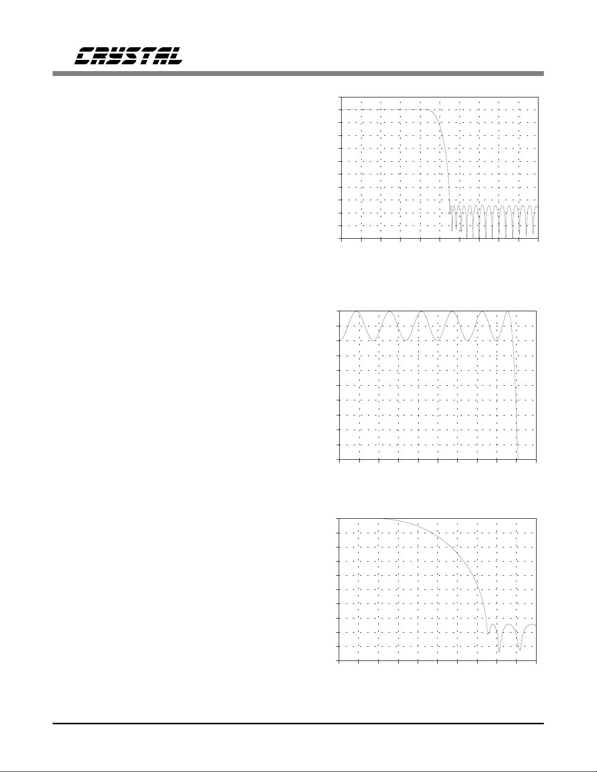
ADC and DAC Filter Response Plots
Figures 21 through 27 show the overall frequency response, passband ripple and transition
band for the CS4215 ADCs and DACs. Figure 27 shows the DACs’ deviation from linear
phase. Fs is the selected sample frequency. Since
the sample frequency is programmable, the filters will adjust to the selected sample frequency.
Fs is also the FSYNC frequency.
10
0
-10
-20
-30
-40
-50
Magnitude (dB)
-60
-70
-80
-90
-100
0.0 0.1 0.2 0.3 0.4 0.5 0.6 0.7 0.8 0.9 1.0
Input Frequency (Fs)
Figure 21. ADC Frequency Response
0.2
0.1
-0.0
-0.1
-0.2
-0.3
Magnitude (dB)
-0.4
-0.5
-0.6
-0.7
-0.8
0.0 0.05 0.10 0.15 0.20 0.25 0.30 0.35 0.40 0.45 0.50
Input Frequency (Fs)
Figure 22. ADC Passband Ripple
0
-10
-20
-30
-40
-50
Magnitude (dB)
-60
-70
-80
-90
-100
0.40 0.42 0.44 0.46 0.48 0.50 0.52 0.54 0.56 0.58 0.60
Input Frequency (Fs)
Figure 23. ADC Transition Band
DS76F2 29

CS4215
10
0
-10
-20
-30
-40
-50
Magnitude (dB)
-60
-70
-80
-90
-100
0.0 0.1 0.2 0.3 0.4 0.5 0.6 0.7 0.8 0.9 1.0
Input Frequency (Fs)
Figure 24. DAC Frequency Response
0
-10
-20
-30
-40
-50
Magnitude (dB)
-60
-70
-80
-90
-100
0.40 0.42 0.44 0.46 0.48 0.50 0.52 0.54 0.56 0.58 0.60
Input Frequency (Fs)
0.2
0.1
-0.0
-0.1
-0.2
-0.3
Magnitude (dB)
-0.4
-0.5
-0.6
-0.7
-0.8
0.00 0.05 0.10 0.15 0.20 0.25 0.30 0.35 0.40 0.45 0.50
Input Frequency (Fs)
Figure 25. DAC Passband Ripple
2.5
2.0
1.5
1.0
0.5
0.0
-0.5
Phase (degrees)
-1.0
-1.5
-2.0
-2.5
0.00 0.05 0.10 0.15 0.20 0.25 0.30 0.35 0.40 0.45 0.50
Input Frequency (Fs)
Figure 26. DAC Transition Band
Figure 27. DAC Deviation from Linear Phase
30 DS76F2

PIN DESCRIPTIONS
XTL1OUT
VD2
DGND2
XTL2IN
XTL2OUT
10
CS4215
TSIN
TSOUT
FSYNC
SCLK
SDOUT
SDIN
DGND1
VD1
CLKIN
CLKOUT
XTL1IN
76
77
79
81
83
85
87
89
91
93
95
97
100
1
2
4
CS4215
100-PIN
6
8
TQFP
(Q)
Top View
75
74
72
70
66
64
PIO1
PIO0
D/C
LOUTR
LOUTL
RESET
PDN
MINR
LINR
MINL
LINL
14
16
18
20
22
24
25
26
33
31
VREF
CMOUT
Note: All unlabeled pins are No Connects
37
35
VA1
AGND1
39
VA2
43
41
MOUT2
AGND2
45
MOUT1
50
60
56
52
51
HEADL
HEADC
HEADR
DS76F2 31

SDIN
DGND1 SDOUT
VD1 SCLK
CLKIN FSYNC
CLKOUT TSOUT
XTL1IN TSIN
XTL1OUT NC
VD2 NC
DGND2 PIO1
XTL2IN PIO0
XTL2OUT D/
RESET NC
PDN LOUTR
NC LOUTL
MINR HEADL
LINR HEADC
7
8
9
10
11
12
13
14
15
16
17 29
18 20 22 24 26 28
1246404244
CS4215
44-PIN
PLCC
(L)
Top View
39
38
37
36
35
34
33
32
31
30
C
MINL HEADR
LINL MOUT1
CMOUT MOUT2
NC NC
VREF AGND2
AGND1 VA2
VA1
CS4215
Power Supply
VA1, VA2 - Analog Power Input, Pins 23(L), 24(L), 37(Q), 39 (Q)
+5 V analog supply.
AGND1, AGND2 - Analog Ground, Pins 22(L), 25(L), 35(Q), 41(Q)
Analog ground. Must be connected to DGND1, DGND2 with zero impedance.
VD1, VD2 - Digital Power Input, Pins 3(L), 8(L), 91(Q), 4(Q)
+ 5 V digital supply.
DGND1, DGND2 - Digital Ground, Pin 2(L), 9(L), 89(Q), 6(Q)
Digital ground. Must be connected to AGND1, AGND2 with zero impedance.
32 DS76F2

CS4215
Analog Inputs
LINL, LINR - Left and Right Channel Line Level Inputs, Pins 18(L), 16(L), 24(Q), 20(Q)
Line level input connections for the right and left channels.
MINL, MINR - Left and Right Channel Microphone Inputs, Pins 17(L), 15(L), 22(Q), 18(Q)
Microphone level input connections for the right and left channels.
Analog Outputs
LOUTR, LOUTL - Line Level Outputs, Pins 33(L), 32(L), 66(Q), 64(Q)
One pair of line level outputs are provided. The output level for right and left outputs can be
independently varied. These outputs can be muted.
HEADR, HEADL - Headphone Outputs, Pins 29(L), 31(L), 52(Q), 60(Q)
HEADR and HEADL are intended to drive a pair of headphones. Additional current drive,
along with an optional +3 dB of gain, ensures reasonable listening levels. These outputs can be
muted.
HEADC - Common Return for Headphone Outputs, Pin 30(L), 56(Q)
HEADC is the return path for large currents when driving headphones from the HEADR and
HEADL outputs. This pin is nominally at 2.1 V.
CMOUT - Common Mode Output, Pin 19(L), 31(Q)
Common mode voltage output. This signal may be used for level shifting the analog inputs. The
load on CMOUT must be DC only, with an impedance of not less than 10kΩ. CMOUT should
be bypassed with a 0.47 µF to AGND. CMOUT is nominally at +2.1V.
MOUT1, MOUT2 - Mono Speaker Outputs, Pins 28(L), 27(L), 45(Q), 43(Q)
Mono external loudspeaker differential output connections. The loudspeaker output is a mix of
left and right line outputs. Independent muting of the speaker is provided. MOUT1 and
MOUT2 output voltage is nominally at 2.1 V with no signal.
VREF - Voltage Reference Output, Pin 21(L), 33(Q)
The on-chip generated ADC/DAC reference voltage is brought out to this pin for decoupling
purposes. This output must be bypassed with a 10 µF capacitor in parallel with a 0.1 µF
capacitor to the adjacent AGND1 pin. No other external load may be connected to this output.
Digital Interface Signals
SDIN - Serial Data Input, Pin 1(L), 87(Q)
Audio data for the DACs and control information for all functions is presented to the CS4215
on this pin.
SDOUT - Serial Data Output, Pin 44(L), 85(Q)
Audio data from the ADCs and status information concerning all functions is written out by the
CS4215 onto this pin.
DS76F2 33

SCLK - Serial Port Clock, Pin 43(L), 83(Q)
SCLK rising causes the data on SDOUT to be updated. SCLK falling latches the data on SDIN
into the CS4215. The SCLK signal can be generated off-chip, and input into the CS4215.
Alternatively, the CS4215 can generate and output SCLK in data mode.
FSYNC - Frame Sync Signal, Pin 42(L), 81(Q)
The Frame Synchronizing Signal is sampled by SCLK, with a rising edge indicating a new
frame is about to start. FSYNC frequency is always the system sample rate. Each frame may
have 64, 128 or 256 data bits, allowing for 1, 2 or 4 CS4215s connected to the same bus.
FSYNC may be input to the CS4215, or may be generated and output by the CS4215 in data
mode. When FSYNC is an input, it must be high for at least 1 SCLK period. FSYNC can stay
high for the rest of the frame, but must return low at least 2 SCLKs before the next frame starts.
TSIN - Time Slot Input, Pin 40(L), 77(Q)
TSIN high for at least 1 SCLK cycle indicates to the CS4215 that the next time slot is allocated
for it to use. TSIN is normally connected to the TSOUT pin of the previous device in the chain.
TSIN should be connected to FSYNC for the 1st (or only) CS4215 in the chain.
TSOUT - Time Slot Output, Pin 41(L), 79(Q)
TSOUT goes high for 1 SCLK cycle, indicating that the CS4215 is about to release the data
bus. Normally connected to the TSIN pin on the next device in the chain.
CS4215
D/C - Data/Control Select Input, Pin 35(L), 70(Q)
When D/C is low, the information on SDIN and SDOUT is control information. When D/C is
high, the information on SDIN and SDOUT is data information.
PDN - Power Down Input, Pin 13(L), 16(Q)
When high, the PDN pin puts the CS4215 into the power down mode. In this mode HEADC
and CMOUT will not supply current. Power down causes all the control registers to change to
the default reset state. In the power down mode, the TSOUT pin remains active, and follows
TSIN delayed by less than 10 ns.
RESET - Active Low Reset Input, Pin 12(L), 14(Q)
Upon reset, the values of the control information (when D/C = 0) will be initialized to the
values given in the Reset Description section of this data sheet.
Clock and Crystal Pins
XTL1IN, XTL1OUT, XTL2IN, XTL2OUT - Crystals 1 and 2 Inputs and Outputs, Pins 6(L),
7(L), 10(L), 11(L), 97(Q), 2(Q), 8(Q), 10(Q)
Input and output connections for crystals 1 and 2. One of these oscillators may provide the
master clock to run the CS4215.
CLKIN - External Clock Input, Pin 4(L), 93(Q)
External clock input optionally used to clock the CS4215. The CLKIN frequency must be
256 times the maximum sample rate (FSYNC frequency).
34 DS76F2

CLKOUT - Master Clock Output, Pin 5(L), 95(Q)
Master clock output, whose frequency is always 256 times the system sample rate (FSYNC
frequency). CLKOUT is active only in data mode and is low during control mode.
Miscellaneous Pins
PIO0, PIO1 - Parallel Input/Output, Pins 36(L), 37(L), 72(Q), 74(Q)
These pins are provided as general purpose digital parallel input/output and have open drain
outputs. An external pull-up resistor is required. They can be read in control mode, and read
and written to in data mode.
Note: All unlabeled pins are No Connects which should be left floating.
CS4215
DS76F2 35

PARAMETER DEFINITIONS
Resolution
The number of bits in the input words to the DACs, and in the output words in the ADCs.
Differential Nonlinearity
The worst case deviation from the ideal codewidth. Units in LSB.
Total Dynamic Range
The rms value of a full scale signal to the lowest obtainable noise floor. It is measured by
comparing a full scale signal to the lowest noise floor possible in the codec (ie. attenuation bits
for the DACs at full attenuation.) Units in dB.
Instantaneous Dynamic Range
The dynamic range available at any instant in time. It is measured using S/(N+D) with a 1 kHz,
-60 dB input signal, with 60 dB added to compensate for the small input signal. Use of a small
input signal reduces to harmonic distortion components of the noise to insignificance. Units in
dB.
CS4215
Total Harmonic Distortion
THD is the ratio of the rms value of a signal’s first five harmonic components to the rms value
of the signals fundamental component. THD is calculated for the ADCs using an input signal
which is 3dB below typical full-scale, and is referenced to typical full-scale. A digital full-scale
output is used to calculate THD for the DACs.
Interchannel Isolation
The amount of 1 kHz signal present on the output of the grounded input channel with 1 kHz
0 dB signal present on the other channel. Units in dB.
Interchannel Gain Mismatch
For the ADCs, the difference in input voltage that generates the full scale code for each
channel. For the DACs, the difference in output voltages for each channel with a full scale
digital input. Units in dB.
Frequency Response
Worst case variation in output signal level versus frequency over 10 Hz to 20 kHz. Units in dB.
Step Size
Typical delta between two adjacent gain or attenuat ion values. Units in dB.
Absolute Step Error
The deviation of a gain or attenuation step from a straight line passing through the
no-gain/attenuation value and the full-gain/attenuation value (i.e. end points). Units in dB.
36 DS76F2

Out-of-Band Energy
The ratio of the rms sum of the energy from 0.46xFs to 2.1xFs compared to the rms full-scale
signal value. Tested with 48kHz Fs giving an out-of-band energy range of 22kHz to 100kHz.
Offset Error
For the ADCs, the deviation in LSBs of the output from mid-scale with the selected input at
CMOUT. For the DACs, the deviation of the output from CMOUT with mid-scale input code.
Units in volts.
CS4215
DS76F2 37

CS4215
APPENDIX A
This data sheet describes version 2 of the CS4215. Therefore, this appendix is included to describe the
differences between versions 0,1 and version 2. This information is only useful for users that still have
version 0 and version 1 devices since version 2 devices will supplant the earlier versions. The version
number can be found in control mode, time slot 7. The version can also be identified by the revision
letter stamped on the top of the actual chip. The revision letter immediately precedes the data code on
the second line of the package marking (See General Information section of the Crystal Data Book).
Version 0 corresponds to chip revision C, version 1 corresponds to chip revision D, and version 2 corresponds to chip revision E. Future chip revisions (ie. F, G, H) may still be version 2 since the version
number only changes if there is a register change to the part that will affect driver software.
The Functional Differences Between V ersion 0(Rev. C) and Version 1(Rev. D)
1. FSYNC on version 0 must be ONLY one SCLK period high, whereas on version 1 FSYNC must be
AT LEAST one SCLK period high.
2. When driving an external CMOS clock into one of the XTL-IN pins, version 0 devices must have a
series resistor of at least 1kΩ between the CS4215 and the clock source. The resistor is needed be-
cause the codec will put XTL-IN to ground (on version 0 only) when that crystal is not selected, as is
the case on power-up. In version 1 the XTL-IN pins are floated when not selected; therefore, the series
resistor is not needed on version 1. Version 1 will work properly if the resistor is included.
3. The OLB and ITS bits do not exist on version 0. Writing these bits as zero makes both versions
function identically; therefore, version 1 is backwards compatible with version 0.
4. When entering control mode, CLKOUT stops 4 to 12 clocks later and may start up briefly when
switching master clock sources on version 0. On version 1 CLKOUT stops within two clocks and
doesn’t start up until data mode is entered.
5. In version 0 the headphone and speaker outputs are not short-circuit protected, whereas in version 1
they are short-circuited protected.
The functional differences between Version 1(Rev. D) and Version 2(Rev. E)
1. The MLB, HPF, and MCK2 bits in control mode do not exist in version 0 or version 1. Writing
these bits as zero makes all versions functionally identical; therefore, version 2 is backwards compatible with previous versions.
2. The A/D invalid bit, ADI, in data mode does not exist in version 0 or version 1.
3. The 8-bit unsigned data format (DF1,0=3) does not exist in version 0 or version 1.
4. SDOUT contained random data during calibration in versions 0 and 1. SDOUT outputs zeros during calibration in version 2.
38 DS76F2

Semiconductor Corporation
CS4215 Evaluation Board
CDB4215
Features
Easy DSP Hook-Up
••
Correct Grounding and Layout
••
Microphone Pre-Amplifier
••
Line Input Buffer
••
Digital Patch Area
••
General Description
The CDB4215 evaluation board allows easy evaluation
of the CS4215 audio multimedia codec. Analog inputs
provided include two
BNC line inputs. Analog outputs provided are two BNC
line outputs, one stereo
pair of speaker terminals.
Digital interfacing is facilitated by two buffered ribbon
cable headers. One contains the serial port and the
other contains the codec control pins.
ORDERING INFORMATION:
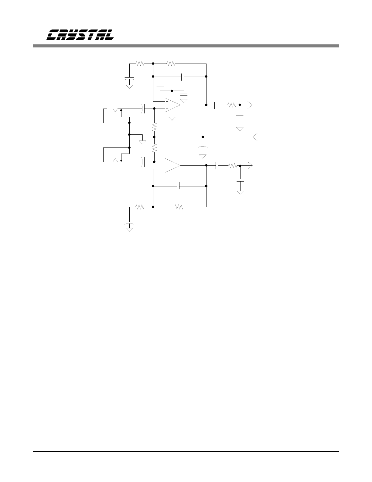
+5VA
AGND +5VDDGND
1
/4" microphone jacks and two
1
/4" headphone jack and one
CDB4215
Microphone
Jacks
Line Inputs
Line Outputs
Headphone
Jack
Speaker
Terminals
Crystal Semiconductor Corporation
P.O. Box 17847, Austin, TX 78760
(512) 445 7222 Fax: (512) 445 7581
A = 23 dB
A = - 6 dB
Digital
I/O
CS4215
Copyright Crystal Semiconductor Corporation 1992
(All Rights Reserved)
Buffers
PIO
Indicators
CLKOUT
CLKIN
Control
Pin
Header
Serial
Port
Header
Digital
Patch
Area
JUL ’93
DS76DB3
39

CDB4215
GENERAL INFORMATION
The CDB4215 is designed to provide an easy
platform for evaluating the performance of the
CS4215 Multimedia Audio Codec. The board
provides a buffered serial interface for easy connection to the serial port of a DSP or other serial
device. A single +5 V power supply is all that is
required to power the evaluation board.
The line input buffers are designed to accept
standard CD-level inputs of 2 V
and BNC-
RMS
to-phono adapters are included to support
various test setups. The microphone inputs consist of two 1/4" mono jacks that are designed to
accept standard single-ended dynamic or condenser microphones.
The line outputs are supplied via BNC jacks
with two more BNC-to-phono adapters. The
headphone output is supplied via a 1/4" stereo
jack and will drive headphones of 48 Ω or
greater. This includes most "walkman" style
headphones. Speaker terminals are provided and
can be connected to speakers with an impedance
of 32 Ω or greater.
header buffer circuitry. Space for a ferrite bead
inductor, L1, has been provided so that the board
may be modified to power the codec from the
digital supply. Selection of L1 will depend on
the characteristics of the noise on the digital supply used.
ANALOG INPUTS
The analog inputs consist of a pair of 1/4" jacks
for two microphones, and a pair of BNC’s for
line level inputs. BNC-to-phono adapters are included to allow testing of the line inputs using
coax or standard audio cables.
The line-level inputs go through a buffer, Figure 2, with a gain of 0.5 which allows input
signals of up to 2 V
RMS
.
The two microphone inputs are single-ended and
are designed to work with both condenser and
dynamic mics. The microphone input buffer circuit, shown in Figure 3, has a gain of 23 dB
thereby defining a full-scale input voltage to the
mic jacks of 19.5 mVpp.
The film plots of the board are included to provide an example of the optimum layout,
ANALOG OUTPUTS
grounding, and decoupling arrangement for the
CS4215.
The CDB4215 includes three analog output
paths: a pair of line output BNC’s, a stereo 1/4"
headphone jack, and a pair of mono speaker ter-
POWER SUPPLY CIRCUITRY
Figure 1 illustrates a portion of the CDB4215
schematic and includes the CS4215 codec along
with power supply circuitry. Power is supplied to
the board via two sets of binding posts, one for
digital and one for analog. The analog supply
must be +5 Volts and supplies power for the en-
minals.
The CS4215 drives the line outputs into an R-C
filter and then to a pair of BNC’s. As with the
line inputs, BNC-to-phono adapters are provided
for flexibility. The line outputs can drive an im-
pedance of 10 kΩ or more, which is the typical
input impedance of most audio gear.
tire codec (both digital and analog power supply
pins) along with the analog input buffers for the
line and microphone inputs. The digital supply is
also +5 Volts and supplies power to the digital
40 DS76DB3
The stereo headphone output can drive headphones with an impedance of 48 Ω or greater.
This includes most "walkman" style headphones.

CDB4215
D2
P6KE
DGND
VD
C32 C30
Microphone
Input Buffer
See Figure 3
Line Input
Buffer
See Figure 2
16.9344 MHz
24.576 MHz
Ferrite Bead
0.1 uF47 uF+
40pF
C24
40pF
C25
40pF
C22
40pF
C23
L1 VA
15
19
17
16
18
10
11
6
7
0.1 uF 1 uF 0.1 uF+
MINR
CMOUT
MINL
LINR
LINL
XTL2IN
XTL2OUT
XTL1IN
XTL1OUT
1 uF+
Y2
Y1
R28
2
C11 C12C13C14
CS4215
U1
23 2438
VA1 VA2VD1 VD2
MOUT1
MOUT2
HEADR
HEADL
HEADC
LOUTR
LOUTL
0.1 uF 47 uF +
C33C31
C34
28
+
22 uF
C16
27
+
22 uF
16
29
R21
R20
31
16
30
R24
600
33
0.0022 uF
NPO
R25
600
32
0.0022 uF
NPO
R52
50 k
R51
50 k
1/2W
1/2W
C27
C26
C29
1 uF
+
C28
1 uF
+
+5VA+5VD
D1
P6KE
AGND
MOUT1
MOUT2
Headphones
LOUTR
39 k
R26
LOUTL
39 k
R27
4
CLKIN
AGND1 AGND2 DGND1
22 25 2
VREF
DGND2
9
21
0.1 uF
C21
+See Fig 5
10 uF
C20
Figure 1. CS4215 & Power Supplies
DS76DB3 41

CDB4215
LINR
LINL
(Mono)
0.47 uF
C17
LT1013
0.47 uF
C37
U3
20 k
R12
20 k
R13
C19
56 pF NPO
VA
10 k
R19
_
2
8
3
+
4
150
1
R14
5 k
+
1 uF
R17
C35
5
+
_
6
150
7
R15
10 k
R18
C18
56 pF NPO
Figure 2. Line Input B uffer
C36
0.1 uF
0.01 uF NPO
C10
C9
0.01 uF
NPO
16
19
18
CS4215
LINR
CMOUT
LINL
MINR
MINL
(Mono)
10 uF
10 uF
R6
1.5 k
+
C6
1 uF
+
C5
C2
+
1 uF
1.5 k
R3
+
C3
VA+
2
3
R5
50 k
R2
50 k
5
6
R4
22.1 k
8
4
C1 560 pF
22.1 k
R1
C4
560 pF
NPO
C8
0.1 uF
1
U2
MC33178
C7
7
NPO
15
19
17
CS4215
MINR
CMOUT
MINL
R56
150
C47
+
1 uF
R57
150
C46
NPO
0.01 uF
NPO
0.01 uF
C48
0.47 uF
C45
0.47 uF
Figure 3. Microphone Input Buffer
42 DS76DB3

CDB4215
Speaker terminals are provided and are labeled
MOUT1 and MOUT2. Speakers connected to the
terminals must have an impedance of 32 Ω or
greater. DC blocking capacitors are included to
form a high-pass filter with the speaker impedance. This filter blocks very low frequency
signals which can heavily distort some inexpensive speakers.
SERIAL INTERFACE
The CDB4215 is primarily designed to evaluate
the CS4215 is single chip mode, i.e. only one
codec on the serial bus. This is the default state
for the CDB4215 and is defined by having the
P4 jumper in the "1CHIP" position, see Figure 4,
which connects FSYNC to TSIN. This connection defines the board codec’s time slots as the
first 64 bits of the frame. The only signals that
need to be connected to the DSP are th e five signals on header J15. The serial interface is
illustrated in Figure 4.
If the goal is to connect multiple CDB4215s on
the same serial port, jumper P4 must be in the
"MULTI" position which disconnects TSIN from
FSYNC. The MULTI position also connects an
unbuffered SDOUT to header J14. This header
pin, SDOUTUB, must be used in lieu of
SDOUT since SDOUT is buffered and does not
go high impedance during other codec’s time
slots. Using the multi-chip scenario, the TSIN
header pin must be connected to the previous
codec’s TSOUT line and the first codec’s TSIN
must be connected, via the header, to FSYNC.
Note that when P4 is in the 1CHIP mode, the
SDOUTUB pin on header J14 is not connected
to the SDOUT pin on the CS4215 and is floating.
There are two scenario’s that must be addressed
when connecting the CDB4215 to a DSP: one is
when the codec is the master in data mode and
the other is when the codec is a slave in data
mode. In control mode the codec is always a
slave and FSYNC and SCLK must be driven
from the DSP. Since the evaluation board buffers
all the signals between the codec and the DSP,
the board must "know" which of the two modes
is being used. Jumper P3 selects the particular
mode.
Codec Master Data Mode
When the codec is to be programmed as a master in data mode, the direction of FSYNC and
SCLK have to be changed between control mode
and data mode. In this case the P3 jumper must
be set for "M/S" which uses the D/C signal to
control the direction of the buffers (U7) for
SCLK and FSYNC. When P3 is set to M/S, the
buffers drive the J15 header in data mode and
receives FSYNC and SCLK from the header in
control mode.
Codec Slave Data Mode
When the codec is to be programmed as a slave
in data mode, FSYNC and SCLK are always inputs to the codec. In this mode P3 must be set to
"SLAVE" which configures the FSYNC and
SCLK buffers to always receive FSYNC and
SCLK from the J15 header.
As stated in the CS4215 data sheet, when the
codec is programmed in slave mode, XCLK = 0
in control mode, SCLK and FSYNC are inputs
and must be derived from the same clock used as
the master clock for the codec. Although SCLK
and FSYNC must be frequency locked to the
master clock, there is no phase requirement.
CONTROL PINS
All control pins, located on header J14, are defined as pins that are not essential to the DSP
serial port when used in 1CHIP mode.
DS76DB3 43
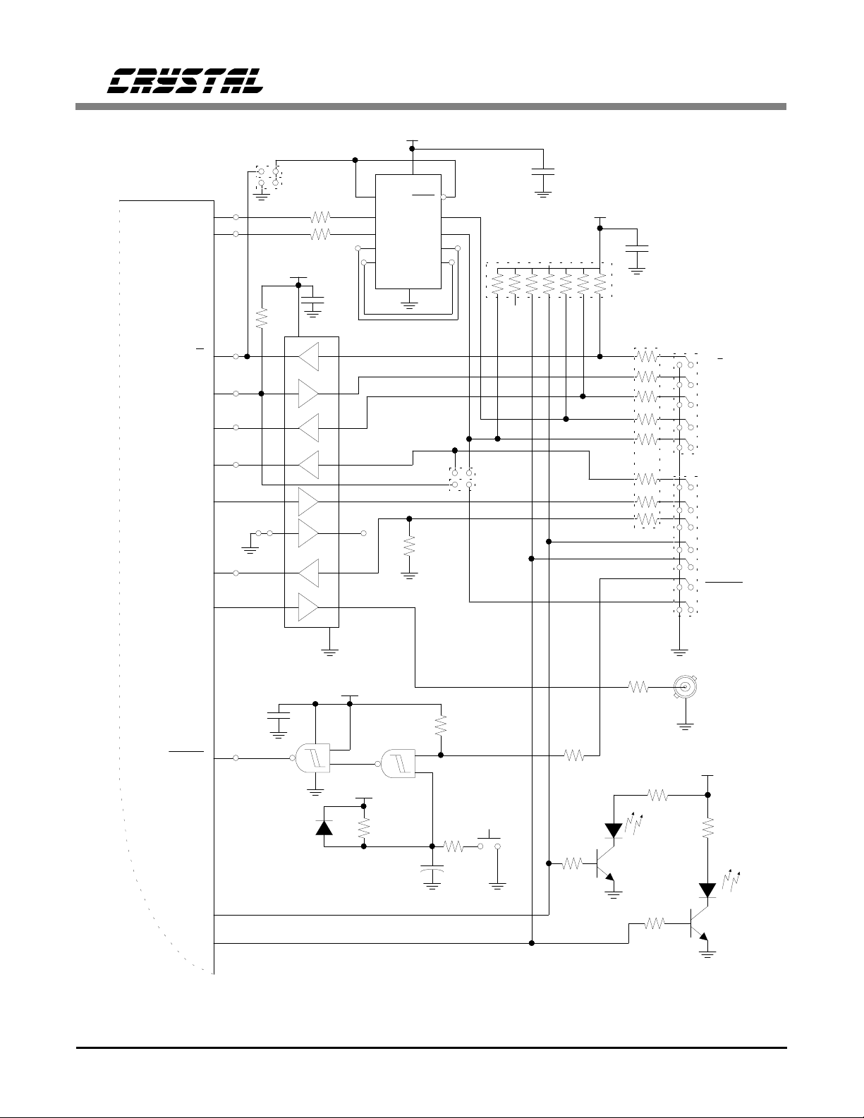
VD
CDB4215
FSYNC
U1
CS4215
SDOUT
TSOUT
CLKOUT
SCLK
D/C
SDIN
TSIN
PDN
43
42
35
44
1
40
41
13
P3
M/S
SLAVE
R43 1 k
R44 1 k
VD
C40
40 k
R49
18
3
16
15
6
713
12
5
9
0.1 uF
20
2
17
4
5
14
8
11
10
13
11
10
9
8
OEB
B0
B1
B2
B3
14
GND
7
OEA
A0
A1
A2
A3
R47
20 k
P4
1
3
4
5
6
C41 0.1 uF
U7
74HCT243
8
1CHIP
MULTI
RP2
20 k SIP
VD
1
2
100 Ohm Dip
16
C49
0.1 uF
RP1
J15
1
D/C
SDOUT
SDIN
SCLK
FSYNC
TSIN
TSOUT
89
PDN
PIO0
PIO1
RESET
SDOUTUB
J14
RESET
PIO0
PIO1
12
36
37
C42
0.1 uF
U4
74HTC541
14
8
U5C
7
D3
IN4148
10
9
VD
VD
6
R7
47 k
U5B
C15
1 uF
R9
20 k
4
5
RESET
100
+
R8
R42
100
PIO0
237 k
R30
Q2,Q3 = MPSA14
Q2
R50
50
D3
R55
800
237 k
R53
CLKOUT
VD
R54800
PIO1
D4
Q3
Figure 4. Digital Interface
44 DS76DB3

CDB4215
PDN and RESET
Power down, PDN, controls the PDN pin on the
codec. The line has an on-board pull-down resistor thereby defining the default state as powered.
This pin only needs to be controlled if the power
down feature is used.
RESET controls the RESET pin on the codec
and is pulled up on the board. This defines the
default state as not reset. This pin only needs to
be controlled if the reset feature on the codec is
needed. Since the codec does require a reset at
power up, a power-up reset circuit is included on
the board. A reset switch is also included to reset
the device without having to remove the power
supply. The power-up reset plus switch are logically OR’ed with the RESET pin on header J14.
PIO Lines
CLOCKS
The CDB4215 can accommodate all clocking
modes supported by the CS4215. A CLKIN
BNC, as shown in Figure 5 allows the CLKIN
pin on the CS4215 to be used as the master
clock source. The two crystals listed in the
CS4215 data sheet are also provided and support
all the audio and multimedia standard sample
frequencies. The master clock is selected via a
CS4215 internal register from control mode.
The CLKOUT BNC is a buffered version of the
CLKOUT pin on the CS4215. CLKOUT is always 256 times the programmed sample
frequency in data mode. CLKOUT is held low in
control mode.
LAYOUT ISSUES
The parallel input/output, PIO, lines are pulled
up on the evaluation board. If they are to be used
as inputs, they should be driven by open-collector gates since inadvertently setting the PIO bits
low in software will force th e external lines low.
The PIO lines are available on header J14.
The PIO lines also go through a high-impedance
buffer and drive LED’s on the evaluation board.
When the LED is on, the corresponding bit is 1
or high. The LED’s provide a visual indication
that may be used to verify that the software is
writing the bits correctly.
CS4215
U5D
11
74HC132
CLKIN
R32
4
1 k
Figure 6 contains the silk screen, Figure 7 contains the top-side copper layer, and Figure 8
contains the bottom-side copper layer of the
CDB4215 evaluation board. These plots are included to provide an example of how to layout a
PCB for the codec. Two of the more important
aspects are the position of the ground plane split,
which is next to the part - NOT UNDER IT, and
the ground plane fill between traces on both layers, which minimizes coupling of radiated
energy.
VD
R16
10 k
13
12
U5A
3
1
2
R29
CLKIN74HC132
5k
Figure 5. CL KIN
DS76DB3 45
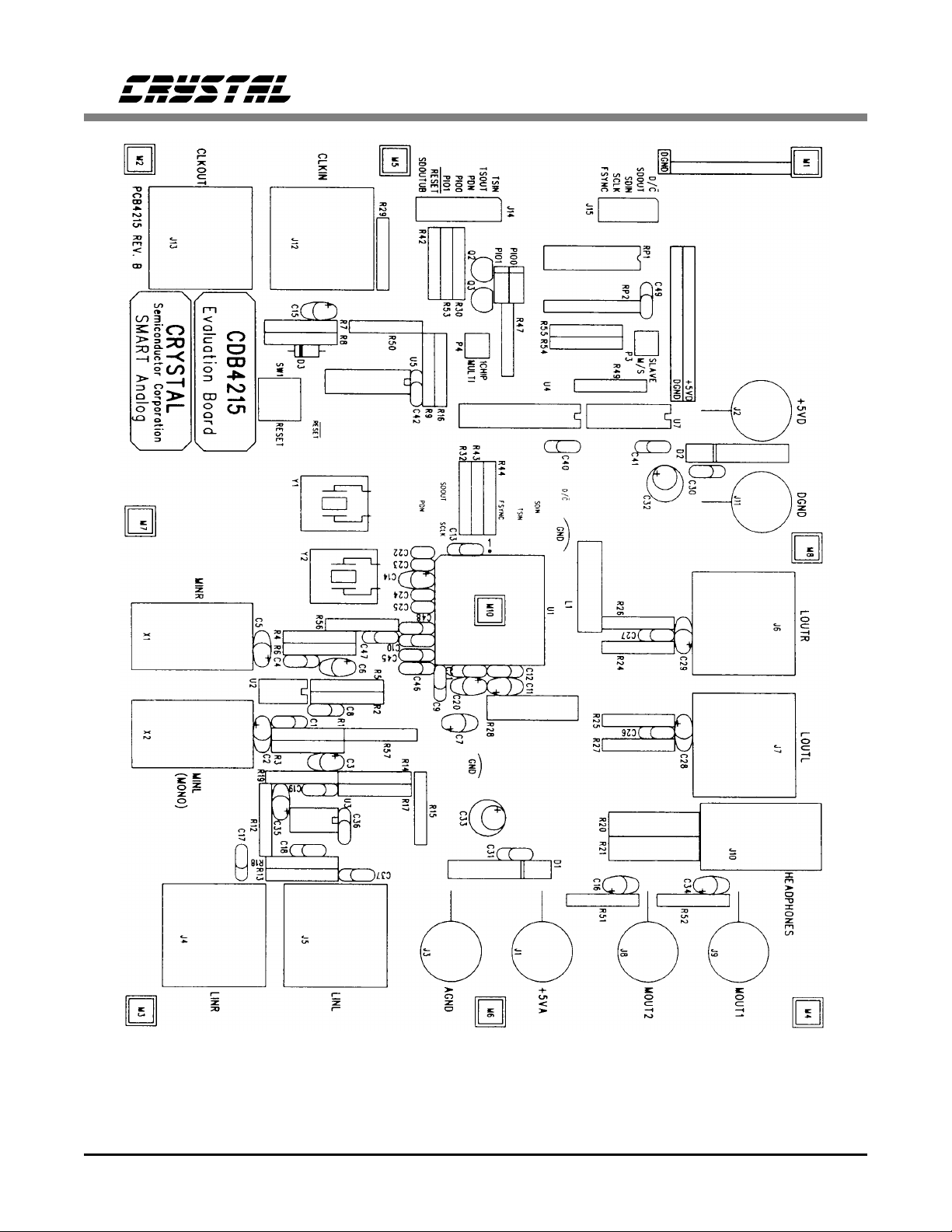
CDB4215
Figure 6. CDB4215 Boa rd Silkscreen (Not to Scal e)
46 DS76DB3

CDB4215
Figure 7. CDB4215 Compont Side Layout ( Not to Scale)
DS76DB3 47

CDB4215
Figure 8. CDB4215 Solder Side Layout ( Not to Scale)
48 DS76DB3

D1
D
E1
44 pin
PLCC
NO. OF TERMINALS
E
DIM
A
A1
B
D/E
D1/E1
D2/E2
e
MILLIMETERS INCHES
NOM
4.45
2.29 0.090
2.79
0.41
17.53
16.59
15.50
1.19 1.35 0.047 0.053
1.27
MAXMIN MAXMIN
4.574.20 0.1800.165
3.04 0.120
0.530.33 0.0210.013
17.6517.40 0.685
16.6616.51 0.650 0.656
16.0014.99 0.590 0.630
NOM
0.175
0.110
0.016
0.690
0.653
0.610
0.050
0.695
D2/E2
e
A1
A
B

D
D1
100 pin
TQFP
E
E1
1
A
C
e
INCHES
MAX
MIN
1.66
0.000
0.26
0.006
0.60 0.024
16.30
14.10
16.30
14.10
0.625
0.70
0.618
0.547
0.618
0.547
0.015 0.025
0.012 0.028
12°
NOM
--
MAX
0.065
--
0.008
0.010
0.020
0.630
0.551
0.630
0.551
0.642
0.555
0.642
0.555
0.020
0.020
0° 12°
DIM
A
A1
B
C
D
D1
E
E1
e
L
∝∝
M
B
MILLIMETERS
MIN
NOM
-
0.00
0.14
0.40 0.016
15.70
13.90
15.70
13.90
0.375
0.30
0°
-
--
0.20
0.51
16.00
14.00
16.00
14.00
0.5
0.51
--
1.00 BSC 0.039 BSC
A1
Terminal
Detail 1
∝∝
L
M

• Notes •

Smart
Analog
TM
is a Trademark of Crystal Semiconductor Corporation
 Loading...