

Page 1
Class D Power Stage
SPKR SU PPLY
VP
GNDPLED
Current Mode Synchronous
Boost Controller
VCOM
Range
Scaling
Class D Front End
Short C ircuit Prot ection
∆Σ Class D Modulator
V
REF
Generation
Bandgap
Voltage
Generation
FILT+
VREF
ISENSE+
ISENSE–/
VSENSE+
GNDA
SCLKLRC K
Soft Ramp
Level Shifters
I²C Control Port
SDASCLSCLK LRCK SDOUT
MCLK
IN–
–
+
9 ,12 ,15, or
18 dB + Mute
IN+
Flash LED Current Driver
Control,
Sensing,
and Fault
Protection
FLOUT1 FLOUT2/AD0FLEN FLINH
SPKOUT+
SPKOUT–/
VSENSE–
I2C Class G Ov erride
Wat chdog
Error
GNDP
VSENSE–
VSENSE+
ISENSE–
ISENSE+
SPKR
SUPPLY
ADC
Serial Audio/Data Port
Serial Port
Cloc k Generation
VA
RESET INT
VMON ADC
Front End
LP
IMON ADC
Front End
LP
Low Bat tery M anagement
Class G
VBST
Current
Sense
IREF+SW
Power
Budgeting
Temperature
Sensor
Overt emp
Protect ion
ADC
ADC
CS35L32
Boosted Class D Amplifier with Speaker-Protection Monitoring
and Flash LED Drivers
Mono Class D Speaker Amplifier
• Two-level Class G operation:
• Boosted: 5 V nominal
• Bypassed: battery voltage is supplied directly
• 2.5-mA quiescent current, monitors powered down
• 1.7 W into 8 (@ 10% THD+N)
• 102-dB signal-to-noise ratio (SNR, A-weighted)
• Idle channel noise 25 Vrms (A-weighted)
• 90% efficiency
Audio Input and Gain
• One differential analog input
• Speaker gain:
• 9, 12, 15, and 18 dB and mute
• Pop suppression, zero-crossing detect transitions
Flash LED Drivers
• Integrated dual LED drivers using the following:
• Boost supply output voltage
• Dual matched current regulators, 750 mA max each
• Programmable setting for Flash Mode current:
50–750 mA, in 50-mA steps
• Programmable setting for Flash-Inhibit Mode current:
50–350 mA, in 50-mA steps
• Programmable setting for Movie Mode current:
150, 120, 100, 80, 60, 40, 20 mA
• Programmable flash timer setting:
50–500 ms, in 25-ms steps
• Dedicated pin for flash trigger (FLEN)
• Dedicated pin for flash inhibit (FLINH)
• Thermally managed through boost-voltage regulation
(Features continue on page 2)
http://www.cirrus.com
Copyright Cirrus Logic, Inc. 2014
(All Rights Reserved)
JUL ‘14
DS963F4
Page 2
CS35L32
Monitors and Protection
•Protection:
• Latched overtemperature shutdown
• Latched amplifier output short circuit shutdown
• LED short or open detection and LED driver shutdown
• Flash inhibit LED current reduction
• Low battery flash LED current reduction
• VP undervoltage lockout (UVLO) shutdown
• Programmable boost inductor current limiting
• Audio and LED shutdown upon stopped MCLK, with
autorecovery
• Interrupt driven error reporting
• Speaker current and voltage monitoring:
• 16-bit resolution
• 60-dB dynamic range (unweighted) for voltage
• 56-dB dynamic range (unweighted) for current
• Bused over I
• Battery voltage monitoring:
• 7-bit resolution
• Bused over I
• System reset
2
S bus
2
S and I2C bus
I2C Control Settings and Registers
• Low-power standby
• LED and audio power budgeting programmable settings
• Boost inductor current limit programmable setting
• Speaker programmable settings:
• Pop suppression through zero-crossing transitions
• Gain and mute
• Battery voltage monitor register, 8 bits
• LED driver programmable settings:
• Flash current register
• Flash inhibit current register
• Movie Mode current register
• Flash timer register
• Error status bit, including the following:
• Stopped MCLK error
• Low battery detection with programmable thresholds
• VP UVLO error
• Overtemperature warning
• Overtemperature error
• Boost converter overvoltage error
• Boost inductor current-limiting error
• Amplifier short-circuit error
• Shorted or open LED error
I2S Reporting
• Monitoring:
• Speaker voltage monitor
• Speaker current monitor
• Battery voltage monitor
• Error reporting:
• VP UVLO shutdown error
• Overtemperature warning
• Overtemperature error
• Boost converter overvoltage error
• Boost inductor current limiting error
• Amplifier short-circuit error
• Speaker voltage monitor overflow error
• Speaker current monitor overflow error
• Battery voltage monitor overflow error
• Status reporting:
• Power-down done
• LED flash event
• LED Movie Mode event
• Flash timer on
Package
• 30-ball WLCSP
Applications
• Smart phones
•Tablets
General Description
The CS35L32 is a low-quiescent power-integrated audio IC, with a mono full-bridge Class D speaker amplifier operating
with a self-boosted Class G supply. Audio input is received differentially. Pop-and-click reduction is achieved with zerocrossing transitions at turn-on, turn-off and upon gain changes. Communication with the host processor is done using an
2C
I
interface. In addition, an I2S bus is used to send monitor and status data.
When two CS35L32 devices are available on the same board, each is identified by its I
or upon deasserting RESET
The speaker amplifier, using closed-loop modulation, achieves low levels of distortion. Class D amplifier efficiency
allows operation at higher speaker power levels without generating excessive heat and without wasting power. Automatic
Class G operation using a boosted supply to the speaker allows for even higher powers and higher crest factor. With a
boosted speaker supply, operation at a fixed 5 V is achieved independently of line supplied battery voltage. The user can
disable Class G operation.
2 DS963F4
, each CS35L32 reads the AD0 pin logic level and configures its I2C device address.
2
C chip address. Upon power-up
Page 3

CS35L32
The battery voltage, speaker voltage, and speaker current signals are monitored, digitized using converters, and
serialized over an I
externally to the CS35L32. Outgoing data is sent over I
monitor data is accessible through I
2
S bus. The speaker monitoring signals are part of a speaker-protection algorithm that is managed
2
C.
2
S with the CS35L32 in Slave or Master Mode. Battery voltage
An integrated dual LED driver operates up to two LEDs in Flash Mode or Movie Mode. A flash event is triggered by an
external signal. A flash-inhibit event is triggered by an external signal, and causes a reduction in flash current. A timer is
provided for flash and flash inhibit events. Movie Mode operation has no timer and starts and ends via an I
Flash and Movie Mode current levels, as well as the flash timer are I
2
C programmable.
2
C command.
Total power consumption when powering LEDs in Flash Mode or Movie Mode, and powering audio simultaneously, is
managed by the user’s choices in programming the current limit and in power budgeting. The primary goal is to manage
audio and LED loads so the boost converter is not current limited and so the CS35L32 does not shut down due to
overheating.
A latched shutdown of the audio amplifier occurs in the event of an output short pin to ground, pin to supply, or pin to pin.
A latched shutdown of the CS35L32 also occurs on overtemperature. An LED driver shutdown occurs in the event of a
shorted or open LED. The CS35L32 shuts down in the event of a battery (VP) undervoltage and autorecovers when the
battery voltage recovers. The CS35L32 shuts down in the event of a stopped MCLK and autorecovers when MCLK
recovers.
The CS35L32 responds to detection of a low battery in the presence of a flash event by reducing flash current and
autorecovers when the battery voltage recovers.
The CS35L32 is reset by asserting RESET
. CS35L32 power up and power down are managed through the RESET pin.
The CS35L32 is available in a 30-ball WLCSP package in the temperature range –10 to +70°C.
DS963F4 3
Page 4

Table of Contents
Table 3-1. Recommended Operating Conditions . . . . . . . . . . . . . . . . . . 8
Table 3-2. Absolute Maximum Ratings . . . . . . . . . . . . . . . . . . . . . . . . . . 8
Table 3-3. DC Characteristics . . . . . . . . . . . . . . . . . . . . . . . . . . . . . . . . . 8
Table 3-4. Boost Converter Characteristics . . . . . . . . . . . . . . . . . . . . . . 9
Table 3-5. LED Drive Characteristics . . . . . . . . . . . . . . . . . . . . . . . . . . . 9
Table 3-6. Speaker Amplifier Output Characteristics . . . . . . . . . . . . . . 10
Table 3-7. Signal Monitoring Characteristics . . . . . . . . . . . . . . . . . . . . 11
Table 3-8. Digital Interface Specifications and Characteristics . . . . . . . 11
Table 3-9. PSRR Characteristics . . . . . . . . . . . . . . . . . . . . . . . . . . . . . 12
Table 3-10. Power Consumption . . . . . . . . . . . . . . . . . . . . . . . . . . . . . 12
Table 3-11. Switching Specifications: Power, Reset, Master Clocks . . 12
Table 3-12. Switching Specifications: ADSP in I
2
S Mode . . . . . . . . . . . 13
Table 3-13. Switching Specifications: I²C Control Port . . . . . . . . . . . . . 14
4.1 Power Supplies . . . . . . . . . . . . . . . . . . . . . . . . . . . . . . . . . . 15
4.2 Interrupts . . . . . . . . . . . . . . . . . . . . . . . . . . . . . . . . . . . . . . . 15
4.3 Speaker Amplifier . . . . . . . . . . . . . . . . . . . . . . . . . . . . . . . . . 16
4.4 Low-Battery Management . . . . . . . . . . . . . . . . . . . . . . . . . . 17
4.5 Undervoltage Lockout (UVLO) . . . . . . . . . . . . . . . . . . . . . . . 18
4.6 Boost Converter . . . . . . . . . . . . . . . . . . . . . . . . . . . . . . . . . . 18
4.7 Die Temperature Monitoring . . . . . . . . . . . . . . . . . . . . . . . . . 18
4.8 Signal Monitoring . . . . . . . . . . . . . . . . . . . . . . . . . . . . . . . . . 19
4.9 LED Driver . . . . . . . . . . . . . . . . . . . . . . . . . . . . . . . . . . . . . . 21
4.10 Power Budgeting . . . . . . . . . . . . . . . . . . . . . . . . . . . . . . . . 23
4.11 Audio/Data Serial Port (ADSP) . . . . . . . . . . . . . . . . . . . . . . 24
4.12 Signaling Format . . . . . . . . . . . . . . . . . . . . . . . . . . . . . . . . 26
4.13 Device Clocking . . . . . . . . . . . . . . . . . . . . . . . . . . . . . . . . . 29
4.14 Control Port Operation . . . . . . . . . . . . . . . . . . . . . . . . . . . . 30
5.1 Required Reserved Register Configuration . . . . . . . . . . . . . 32
5.2 Avoiding Current Transients when Issuing a Flash Event . . 32
5.3 External Component and PCB Design Considerations—EMI Out-
put Filtering . . . . . . . . . . . . . . . . . . . . . . . . . . . . . . . . . . . . . . . . . 33
5.4 PCB Routing Considerations for Thermal Relief . . . . . . . . . 33
5.5 Inductor Selection . . . . . . . . . . . . . . . . . . . . . . . . . . . . . . . . . 34
6 Register Quick Reference . . . . . . . . . . . . . . . . . . . . . . . . . . . . . 35
7 Register Descriptions . . . . . . . . . . . . . . . . . . . . . . . . . . . . . . . . 36
7.1 Device ID A and B . . . . . . . . . . . . . . . . . . . . . . . . . . . . . . . . 36
7.2 Device ID C and D . . . . . . . . . . . . . . . . . . . . . . . . . . . . . . . . 36
7.3 Device ID E . . . . . . . . . . . . . . . . . . . . . . . . . . . . . . . . . . . . . 36
7.4 Revision ID . . . . . . . . . . . . . . . . . . . . . . . . . . . . . . . . . . . . . . 36
7.5 Power Control 1 . . . . . . . . . . . . . . . . . . . . . . . . . . . . . . . . . . 36
7.6 Power Control 2 . . . . . . . . . . . . . . . . . . . . . . . . . . . . . . . . . . 37
7.7 Clocking Control . . . . . . . . . . . . . . . . . . . . . . . . . . . . . . . . . . 37
7.8 Low Battery Thresholds . . . . . . . . . . . . . . . . . . . . . . . . . . . . 37
7.9 Battery Voltage Monitor . . . . . . . . . . . . . . . . . . . . . . . . . . . . 38
7.10 Boost Converter Peak Current Protection Control . . . . . . . 38
7.11 Scaling . . . . . . . . . . . . . . . . . . . . . . . . . . . . . . . . . . . . . . . . 38
7.12 LED and Audio Power-Budget Management . . . . . . . . . . . 38
7.13 ADSP Control . . . . . . . . . . . . . . . . . . . . . . . . . . . . . . . . . . . 39
7.14 Class D Amplifier Control . . . . . . . . . . . . . . . . . . . . . . . . . . 39
7.15 Protection Release Control . . . . . . . . . . . . . . . . . . . . . . . . 39
7.16 Interrupt Mask 1 . . . . . . . . . . . . . . . . . . . . . . . . . . . . . . . . . 40
7.17 Interrupt Mask 2 . . . . . . . . . . . . . . . . . . . . . . . . . . . . . . . . . 40
7.18 Interrupt Mask 3 . . . . . . . . . . . . . . . . . . . . . . . . . . . . . . . . . 41
7.19 Interrupt Status 1 (Audio) . . . . . . . . . . . . . . . . . . . . . . . . . . 41
7.20 Interrupt Status 2 (Monitors) . . . . . . . . . . . . . . . . . . . . . . . . 42
7.21 Interrupt Status 3 (LEDs and Boost Converter) . . . . . . . . . 42
7.22 LED Lighting Status . . . . . . . . . . . . . . . . . . . . . . . . . . . . . . 43
7.23 LED Flash Mode Current . . . . . . . . . . . . . . . . . . . . . . . . . . 43
7.24 LED Movie Mode Current . . . . . . . . . . . . . . . . . . . . . . . . . . 44
7.25 LED Flash Timer . . . . . . . . . . . . . . . . . . . . . . . . . . . . . . . . 44
7.26 LED Flash Inhibit Current . . . . . . . . . . . . . . . . . . . . . . . . . . 44
8 Typical Performance Plots . . . . . . . . . . . . . . . . . . . . . . . . . . . . 45
8.1 System-Level Efficiency and Power-Consumption Plots . . . 45
8.2 Audio Output Typical Performance Plots . . . . . . . . . . . . . . . 46
8.3 Monitoring Typical Performance Plots . . . . . . . . . . . . . . . . . 47
9 Parameter Definitions . . . . . . . . . . . . . . . . . . . . . . . . . . . . . . . . 49
10 Package Dimensions . . . . . . . . . . . . . . . . . . . . . . . . . . . . . . . . 50
11 Thermal Characteristics . . . . . . . . . . . . . . . . . . . . . . . . . . . . . 50
12 Ordering Information . . . . . . . . . . . . . . . . . . . . . . . . . . . . . . . . 50
13 References . . . . . . . . . . . . . . . . . . . . . . . . . . . . . . . . . . . . . . . . 51
14 Revision History . . . . . . . . . . . . . . . . . . . . . . . . . . . . . . . . . . . . 51
CS35L32
4 DS963F4
Page 5
1 Pin Descriptions
A1A2A3
A4A5A6B1B2B3B4B5B6
C1C2C3C4C5C6D1D2D3D4D5D6E1E2E3E4E5
E6
General Ground
LED Digital I/O
Power Supply
Boost Converter
Audio
Digital I/O
CS35L32
1 Pin Descriptions
‘‘‘
‘
‘
SDA SCL SDOUT SCLK MCLK FLOUT2/
‘‘‘‘‘
AD0
VP INT RESET LRCK GNDPLED FLOUT1
‘‘‘‘‘
SW GNDP GNDP FLINH GNDA VA
‘‘‘‘‘
SW SPKOUT+ SPKOUT–/
‘‘‘‘‘
VSENSE–
FLEN IREF+ FILT+
VBST SPKRSUPPLY IN– IN+ ISENSE–/
VSENSE+
Figure 1-1. Top-Down (Through-Package) View—30-Ball WLCSP Package
Table 1-1. Pin Descriptions
Ball Name
Ball
Number
SDA A1 VA I/O I
Power
Supply
I/O Ball Description
2C
Serial Data Input. Serial data for the I2C
serial port
2C
SCL A2 VA I I
Clock Input. Serial clock for the I2C serial
port
MCLK A5 VA I Master Clock Source. Clock source for A/D
converters and audio/data serial port (ADSP).
MCLK
blocks (see Section 4.13 and Section 7.7).
, derived from MCLK, is used for other
INT
SCLK A4 VA I/O Serial Clock. Serial shift clock for the serial
audio interface
LRCK B4 VA I/O Left Right Clock. Determines which channel,
left or right, is currently active on the serial
audio/data lines
SDOUT A3 VA O Serial Audio/Data Output. I²S serial data
output used to monitor voltage and current of
SPKOUT signal and VP levels
INT
B2 VA O Interrupt. Programmable, open-drain, active-
low programmable interrupt output
Internal
Connection
Weak pulldown
(~1 M
Weak pulldown
(~1 M
Weak pulldown
(~1 M
Weak
pull-down
(~1 M
ISENSE+
Driver Receiver
—CMOS
open-drain
output
Hysteresis
on CMOS
input
——Hysteresis
State at
Reset
Hi-Z
Hi-Z
on CMOS
input
— Hysteresis
on CMOS
Pulled
down
input
CMOS
output
Hysteresis
on CMOS
Pulled
down
input
CMOS
output
Hysteresis
on CMOS
Pulled
down
input
CMOS
output
—CMOS
— Pulled
down
—Hi-Z
open-drain
output
DS963F4 5
Page 6
RESET
LED
Boost Converter
Audio
Power Supply
General Ground
Ball Name
Table 1-1. Pin Descriptions (Cont.)
Ball
Number
Power
Supply
B3 VA I Reset. When asserted, the device enters a
I/O Ball Description
low-power mode, outputs are set to Hi-Z, and
I²C register values are set to defaults. Outputs
are Hi-Z except those with weak pull-ups or
pull-downs as mentioned.
1 Pin Descriptions
Internal
Connection
— — Hysteresis
Driver Receiver
CS35L32
State at
Reset
Low
on CMOS
input
FLEN D4 VA I Flash Enable. Input signal commanding a
FLINH C4 VA I Flash Inhibit. Input signal determining
FLOUT1 B6 SPKR
SUPPLY
FLOUT2/AD0 A6 SPKR
SUPPLY
VBST E1 — O Boost Converter Output. Output of boosted
SPKRSUPPLY E2 — I Speaker Supply. Full-bridge Class D speaker
SW C1, D1 VBST I Boost Converter Switch Node. Connects the
IREF+ D5 VA I Current Reference Resistor. Connection for
flash event into both LEDs. It is asserted high.
whether the LEDs are in Flash Mode (logic
low) or Flash-Inhibit Mode (logic high, LED
current reduced).
O LED Driver 1. Output driving LED 1 by sinking
current from the LED cathode
I/O LED Driver 2/Address Zero. Output driving
LED 2 by sinking current from the LED
cathode. AD0 programs the chip address
when RESET
tying the pin to ground clears the chip address
LSB. Otherwise, the LSB is set.
supply. This pin cannot be used to drive any
external loads other than the on chip Class D
Amplifier and Flash LEDs.
amplifier power supply.
inductor to the rectifying switch.
an external resistor to be used for generating
the CS35L32’s internal main current reference.
See Fig. 2-1 for required resistor value.
is deasserted. If no LED is used,
Weak pulldown
(~1 M
Weak pulldown
(~1 M
Weak pull-up
(~1 M
Weak pull-up
(~1 M
————
——
————
————
— Hysteresis
on CMOS
input
— Hysteresis
on CMOS
input
— — SPKR
— — SPKR
Pulled
down
Pulled
down
SUPPLY
SUPPLY
IN+ E4 SPKR
IN– E3 SPKR
SPKOUT+
SPKOUT–/VSENSE–D2D3
ISENSE+
ISENSE–/VSENSE+E6E5
FILT+ D6 VA O Positive Voltage Reference. Positive
VA C6 — I Analog Input Power. Power supply for
VP B1 — I Boost Converter Input Power. Power supply
GNDA C5 — Analog Ground. Ground reference for the
GNDP C2, C3 — Power Ground. Ground reference for boost
GNDPLED B5 — LED Power Ground. Ground reference for
SUPPLY
SUPPLY
SPKR
SUPPLY
SPKR
SUPPLY
I Input 1 Differential Positive Line. Positive
analog input
I Input 1 Differential Negative Line. Negative
analog input
O Speaker Differential Audio Output. Internal
Class D speaker amplifier output. SPKOUT–
serves as voltage monitor negative sense pin
(VSENSE–).
I Current Sense Inputs. Sense voltage across
an external resistor in series with SPKOUT+.
ISENSE– serves as voltage monitor positive
sense pin (VSENSE+).
reference for internal circuits
internal analog section
or battery voltage powering boost converter
internal analog section of the IC
converter and Class D amplifier’s output stage
LED current return. Should be tied to ground
plane.
————
————
———Hi-Z
————
————
————
————
————
————
————
6 DS963F4
Page 7

2 Typical Connection Diagram
Batter y
1 H
C
OUT
0.1
0.1 F
**
L
BST
44.2 k
R
BST_SNS
8
C
OUT
**
Applications
Processor
0.1 F
10 F
C
BST
*
*
RPRPRP_
I
PMU
10 F
*
0.1 F
VA
*
4.7 F
*
Line Input 1
CS35L32
ISENSE–/
VSENSE +
SPKOUT+
ISENSE+
IREF+
SPKOUT–/
VSENSE–
VBST
GNDP
FLOUT1
FLOUT2 / AD0
GNDPLED
SPKRSUPPLY
SDOUT
LRCK
SCLK
MCLK
FLEN
FLINH
SCL
SDA
INT
RESET
VA
FILT+
GNDA
IN+
IN–
VP SW
*
*
3.0–5.25 V
1.71–1.89 V
10 F
Notes:
• All external passive component values are nominal values.
Key for capacitor types required:
* Use low ESR, X7R/X5R capacitors.
** Use low ESR, X7R capacitors.
If no type symbol is shown next to a capacitor, any type may be used.
• As required, add protection circuitry to ensure compliance with the absolute maximum ratings in Tab le 3 -2 .
1. C
BST
is a ceramic capacitor and derates at DC voltages higher than 0 V. In this application, the capacitor should not derate to a value lower
than 4 F across the specified boost output voltage in Tab le 3 -4 . Capacitor tolerance and the temperature coefficient should also be taken
into account to guarantee the 4-F value.
2. Minimum pull-up resistor values are selected in accordance with the Table 3-8 V
OL
specification. Maximum pull-up resistances are selected
based on load capacitance and relevant switching specs (Table 3-13).
3. Select each capacitor to be 0.22 F for an 18-Hz passband @ 12-dB amplifier gain, for a 3-dB roll-off. The equation for calculating the
capacitance for a given passband is C = 1/( * f * R
INDIF
), where C is in F, R
INDIF
is the differential input resistance in and f is in Hz (see
the differential input resistance specification in Tab l e 3- 3). Signals IN+ and IN– are subject to the recommended ranges in Table 3-1.
4. R
BST_SNS
is inherently tied to the accuracy of the BST_IPK current limit. A resistor with a 0.1% tolerance is required for this component to
meet the specified IMAX(B) max and min values in Table 3-4.
5. The required tolerance on the 0.1- ISENSE resistor is 1%. The required temperature coefficient is ±200 ppm/°C.
6. C
OUT
capacitors are optional EMI suppressors used with CS35L32 edge-rate control, depending on application requirements. Because
switching losses increase linearly with increases to these capacitances, it is recommended that C
OUT
values not exceed 2 nF. The
recommended value is 470 pF.
7. LED and I
2
C addressing options:
VBST VBST
c) AD0 = 1 d) AD0 = 0b) AD0 = 1a) AD0 = 1
VBST VBST
FLOUT1 FLOUT2 FLOUT1 FLOUT2 FLOUT1 FLOUT2FLOUT1 FLOUT2
NC
See Note 7 for LED
and I
2
C addressing
options.
Note 1
Note 3
Note 2
Note 5
Note 4
Note 6
CS35L32
2 Typical Connection Diagram
Figure 2-1. Typical Connection Diagram
DS963F4 7
Page 8
CS35L32
3 Characteristics and Specifications
3 Characteristics and Specifications
Table 3-1. Recommended Operating Conditions
GNDA = GNDP = 0 V, all voltages with respect to ground. Device functional operation is guaranteed within these limits. Functionality is not guaranteed
or implied outside of these limits. Operation outside of these limits may adversely affect device reliability.
Parameters Test Conditions Symbol Min Max Units
DC power supply Analog (and digital I/O and core) — VA 1.71 1.89 V
Battery — VP 3.0 5.25 V
External voltage applied to analog inputs powered by VA (IREF+, FILT+)
External voltage applied to analog inputs powered by SPKRSUPPLY (IN+,
IN–, ISENSE+, ISENSE–,VSENSE+, VSENSE–)
External voltage applied to digital inputs — V
Ambient temperature — TA –10 +70 °C
1.The maximum overvoltage/undervoltage is limited by the input current.
Table 3-2. Absolute Maximum Ratings
GNDA = GNDP = 0 V; all voltages with respect to ground. Operation at or beyond these limits may permanently damage the device.
Parameters Test Conditions Symbol Min Max Units
DC power supply Analog — VA –0.3 2.22 V
Input current
1
Ambient operating temperature (local to device, power applied) — T
Junction operating temperature (power applied) — T
Storage temperature — T
1.Any pin except supplies. Transient currents of up to ±100 mA on the analog input pins do not cause SCR latch up.
Table 3-3. DC Characteristics
Test conditions, except where noted otherwise: VA = 1.8 V, VP = 3.6 V, VBST = 5.0 V, GNDA = GNDP = 0 V, TA = +25°C.
Parameters Symbol Test Conditions Min Typical Max Units
Differential Input resistance (IN+ to IN–) R
FILT+ voltage — — — VA — —
Overtemperature shutdown threshold T
Overtemperature warning threshold T
Overtemperature warning threshold deviation — — — ±10 — °C
Low battery threshold — LOWBAT_TH = 00
Low-battery recovery threshold — LOWBAT_RECOV = 001
VP undervoltage lockout threshold (VP falling) UVLO — — 2 — V
VP undervoltage lockout hysteresis — — — 100 — mV
1
—V
—V
INAS
INSS
INDI
–0.3 VA + 0.3 V
–0.3 SPKRSUPPLY + 0.3 V
–0.3 VA + 0.3 V
Battery — VP –0.3 6.0 V
—IIN—±10mA
–40 +115 °C
–40 +150 °C
–65 +150 °C
—
—
—
—
63
51
40
31
— — 150 — °C
— — 135 — °C
—
3.10
—
3.20
—
3.30
—
3.40
—
3.20
—
3.30
—
3.40
—
3.50
—
3.60
INDIF
OP
WRN
A
J
STG
Amp gain = 9 dB
Amp gain = 12 dB
Amp gain = 15 dB
Amp gain = 18 dB
LOWBAT_TH = 01
LOWBAT_TH = 10
LOWBAT_TH = 11
LOWBAT_RECOV = 010
LOWBAT_RECOV = 011
LOWBAT_RECOV = 100
LOWBAT_RECOV = 101–11x
—
—
—
—
—
—
—
—
—
—
—
—
—
k
k
k
k
V
V
V
V
V
V
V
V
V
8 DS963F4
Page 9
CS35L32
3 Characteristics and Specifications
Table 3-4. Boost Converter Characteristics
Test conditions, except where noted otherwise: VA = 1.8 V, VP = 3.6 V, VBST = 5.0 V, amp gain = 12 dB, GNDA = GNDP = 0 V, TA = +25°C, MCLK
= 6 MHz. MCLK
is explained in Section 4.13.1 and Section 7.7.
INT
Parameters Symbol Test Conditions Min Typical Max Units
Boost output voltage VBST Boosting
Bypass
Boost output voltage tolerance VBST No load: I
Load regulation V
Line regulation V
Boost FET peak-current limit
(See Section 7.10.)
I
MAX(B)
3.0 V < VP < 4.2 V; I
(Load)
(Line)
3.0 V< VP < 4.2 V; I
LOAD
BST_IPK = 0000 0000
BST_IPK = 0010 0000
BST_IPK = 0100 0000
LOAD
= 0.25A to1.5 A — 60 — mV/A
= 0 A, 500 mA — 40 — mV/V
LOAD
BST_IPK = 0110 0000
BST_IPK = 1000 0000
Output switching frequency
1
Boost FET ON resistance R
Boost FET ON resistance temp coefficient — I
Rectifying FET ON resistance R
Rectifying FET ON resistance temp coefficient I
Overvoltage detection threshold V
Threshold Class G On, IN+ to IN– V
Threshold Class G Off, IN+ to IN– V
f
SW(B)
DS(ON)B
DS(ON)R
OVTH
IN1THON
IN1THOF
I
OUT(B)
OUT(B)
I
OUT(B)
OUT(B)
Boost enabled — 5.5 5.7 V
VBST = VP = 3.6 V — 0.60 — V
VP = 3.6 V, VBST = 5 V — 0.33 — V
Minimum Class G boost ON hold-off time — VP = 3.6 V, VBST = 5 V — 800
Operating efficiency
1.MCLKDIV2 (see p. 37) should be configured so MCLK
2.Minimum Class G boost ON hold-off time is determined from when the low audio detection is latched until when the boost is turned off. The latching
mechanism occurs in 800-ms intervals. If the audio level is detected as low between two sequential latches, the hold-off time is extended by the
difference between when the detection occurs and the subsequent latch pulse. This may extend the hold-off time up to 1.6 s in extreme cases.
3.Efficiency specified here assumes the boost converter drives an external resistive load via the VBST pin, instead of the onboard Class D amplifier.
Table 3-5. LED Drive Characteristics
Test conditions, except where noted otherwise: VA = 1.8 V, VP = 3.6 V, VBST = 5.0 V, GNDA = GNDP = GNDPLED = 0 V, TA = +25°C.
3
B
is 6 or 6.1440 MHz (see Table 4-14) for boost-converter operation at 2 or 2.05 MHz.
INT
VBST = 5 V, I
VBST = 5 V, I
OUT(B)
OUT(B)
= 500 mA
=1.5 A——
VP*1.15
—
—
VP
5.4
—
=0 mA –5 — +5 %
—
—
—
—
—
—— MCLK
2.89
3.30
3.72
4.14
4.56
/3 — MHz
INT
—
—
—
—
—
= 1 A — 80 — m
= 1 A — 0.2 — %/oC
= 1 A — 150 — m
= 1 A — 0.2 — %/oC
2
90
85
—ms
—
—
Parameters Min Typical Max Units
Flash Mode current settings, per LED
(Step size = 50 mA)
Flash Inhibit Mode current settings, per LED
(Step size = 50 mA)
Movie Mode current settings, per LED
1
1
1
LED_FLCUR = 1111
…
LED_FLCUR = 0001
LED_FLINHCUR = 0111
…
LED_FLINHCUR = 0001
LED_MVCUR = 111
LED_MVCUR = 110
LED_MVCUR = 101
LED_MVCUR = 100
LED_MVCUR = 011
LED_MVCUR = 010
LED_MVCUR = 001
—
…
—
—
…
—
—
—
—
—
—
—
—
750
…
50
350
…
50
150
120
100
80
60
40
20
—
…
—
—
…
—
—
—
—
—
—
—
—
LED current accuracy –10 — +10 %
LED current matching —10—%
Flash timer (t
) MCLK
flash
MCLK
= 6 MHz 2; TIMER = 1 0010–1 1111
INT
TIMER = 0 0001
TIMER = 0 0000
= 6.144 MHz; TIMER = 1 0010–1 1111
INT
TIMER = 0 0001
TIMER = 0 0000
—
—
—
—
—
—
500
75
50
488.3
73.2
48.8
—
—
—
—
—
—
LED flash timer accuracy 0—+1ms
LED flash inhibit time (FLINH high to LED current 3% settling) — 40 — s
1.Flash or Movie Mode current is delivered from the boost converter’s output, which provides a voltage higher than the LED voltage. Depending on the
LED voltage requirement and on VP supply voltage, the boost converter is internally controlled to boost or be in bypass (rectifying FET fully on).
2.The flash time setting is generated from MCLK
. MCLKDIV2 (see p. 37) should be configured so MCLK
INT
is 6 or 6.1440 MHz. See Table 4-14.
INT
V
V
A
A
A
A
A
%
%
mA
…
mA
mA
…
mA
mA
mA
mA
mA
mA
mA
mA
ms
ms
ms
ms
ms
ms
INT
DS963F4 9
Page 10
CS35L32
Generic Simulated
Speaker Load
R
SENSE
0.1
Audio Precision AP2700
Audio Analyzer
Audio Precision
AUX-0025 Filter
SPKOUT+
ISENSE+
SPKOUT–
ISENSE–/
VSENSE+
VSENSE–
SPKRSUPPLY
5 V
3.6 V
1.8 V
VP
VA
8
33 H
3 Characteristics and Specifications
Table 3-6. Speaker Amplifier Output Characteristics
Test conditions, except where noted otherwise: VA = 1.8 V, VP = 3.6 V, VBST = 5.0 V, 1-kHz input, amp gain = 12 dB, GNDA = GNDP = 0 V, TA = +25°C,
measurement bandwidth is 20 Hz to 20 kHz, Fs = 48 kHz, MCLK
Parameters Symbol Test Conditions Min Typical Max Units
Continuous average power delivered to load
1
Po 8- load, THD 10%
THD+N THD+N 8- load, 1.0 W — 0.02 — %
Input voltage @ 1% THD+N V
ICLIP
Signal to noise ratio SNR Referenced to output voltage @1% THD+N, A-weighted — 102 — dB
Idle channel noise ICN VBST = VP, A-weighted — 25 — Vrms
Common-mode rejection ratio CMRR V
Frequency response FR 20 Hz to 20 kHz, No input DC blocking caps –0.1 0 0.1 dB
Efficiency
2
A
Class D amplifier gain — AMP_GAIN = 000 (mute)
N-FET ON resistance R
P-FET ON resistance R
Output DC offset voltage V
Time from shutdown to audio out t
DS ON,N
DS ON,P
OFFSET
SD RESET
1.Power delivered to the speaker from the 0.1- load side terminal (refer to Fig. 2-1).
2.Efficiency collected using a 5-V external supply, as shown
in the drawing. For this test, the VBST pin should not be
connected to the SPKRSUPPLY pin.
= 6 MHz. MCLK
INT
is explained in Section 4.13.1 and Section 7.7.
INT
1.75
8- load, THD 1%——
1.45——WW
8- load — 0.84 — Vrms
ripple
= 1 VPP, f
= 217 Hz — 55 — dB
ripple
8- load 33 H, 1.7 W — 91 — %
AMP_GAIN = 001
AMP_GAIN = 010
AMP_GAIN = 011
AMP_GAIN = 100
I
= 0.5 A — 185 — m
FET
I
= 0.5 A — 205 — m
FET
–80
—
—
—
—
12
15
18
—
—
—
—
—
dB
dB
dB
dB
dB
9
—
Inputs AC coupled to ground — ±5 — mV
deasserted, zero-crossing disabled — 15 — ms
10 DS963F4
Page 11
CS35L32
VSENSE+
217 Hz
500 mV
PP
DC Offset = 0
VSENSE–
3 Characteristics and Specifications
Table 3-7. Signal Monitoring Characteristics
Test conditions, except where noted otherwise: VA = 1.8 V, VP = 3.6 V, VBST = 5.0 V, amp gain = 12 dB, 0.1- sense resistor, GNDA = GNDP = 0 V,
T
= +25°C. Measurement bandwidth is 20 Hz to 20 kHz, Fs = 48 kHz, Input Signal = 1 kHz, MCLK
A
and Section 7.7.
Parameters Min Typical Max Units
General ADC characteristics Power-up time: t
VSENSE± monitoring
characteristics (VMON)
Dynamic range (unweighted), VSENSE± = ±5.0 V (10 V
Total harmonic distortion + noise, –3.8 dBFS
Full-scale signal input voltage 6.59•VA 6.94•VA 7.29•VA V
Common-mode rejection ratio (217 Hz @ 500 mVPP)
ISENSE± monitoring
characteristics (IMON)
Dynamic range (unweighted), ISENSE± = ±0.625 A (1.25 A
Total harmonic distortion, –29.5 dBFS
Full-scale signal input voltage 1.56•VA 1.64•VA 1.72•VA V
VMON-to-IMON isolation
VP monitoring characteristics Data width — 8 — Bits
Voltage resolution (See the equation in Section 4.8.4.) — 35.3 — mV
(FF code) signal input voltage (VP) 2.89•VA 3.05•VA 3.20•VA V
VPMON = 1011 0011
VPMON = 1011 0100
VPMON = 1111 1111
VPMON = 0000 0000
1.Typical value is specified with PDN_AMP and PDN_xMON bits initially set. Maximum power-up time is affected by the actual MCLK
2.Parameters given in dB are referred to the applicable typical full-scale voltages. Applies to all THD+N and resolution values in the table
3.VSENSE± THD is measured with the Class D amplifier as the audio source connected to an 8- + 33H speaker load, supplied by a 6.3-VPP, 1-kHz
sine wave, operating under the typical performance test conditions to produce a large, unclipped audio signal. This setup produces a –3.8-dBFS
VMON output. Larger Class D amplifier amplitudes begin to exhibit clipping behavior, increasing distortion of the signal supplied to VSENSE±
4.CMRR test setup for VSENSE±:
= 6 MHz, MCLK
INT
PUP(ADC)
is explained in Section 4.13.1
INT
—8.5
[1]
Data width — 16 — Bits
)— 60 — dB
PP
3
— –60 — dB
4
—60—dB
Group delay
5
—7.6/Fs— s
Data width — 16 — Bits
)— 56 — dB
PP
6
— –45 — dB
7
—56—dB
Group delay
8
—7.6/Fs— s
…
—
—
…
—
—
2.8
2.835
…
5.482
5.518
—
—
…
—
—
frequency.
INT
ms
2
2
PP
2
2
2
PP
2
V
V
…
V
V
5.VMON group delay is measured from the time a signal is presented on the VSENSE± and pins until the MSB of the digitized signal exits the serial
port. Fs is the LRCK rate.
6.For reference, injecting a 125-mVpp fully differential sine wave into the ISENSE± pins (equivalent to a ±0.625 A current with a 0.1- ISENSE resistor)
produces an IMON output of –29.5 dBFS (since typical full-scale is 1.64*VA, in V
amplifier as the audio source, which is connected to an 8- + 33-H speaker load, supplied by a 7.0-V
). ISENSE± monitoring THD is measured using the Class D
PP
, 1-kHz sine wave, operating under the
PP
typical performance test conditions to produce a large, unclipped audio signal. This setup produces a –29.5-dBFS amplitude IMON output. Larger
Class D amplifier amplitudes begin to exhibit clipping behavior, increasing the distortion of the signal supplied to ISENSE±.
7.VMON-to-IMON isolation is the error in the current sense due to VMON, expressed relative to full-scale sense current in decibels.
8.IMON group delay is measured from when a signal is presented on the ISENSE± pins until the MSB of the digitized signal exits the serial port. Fs is
the LRCK rate.
Table 3-8. Digital Interface Specifications and Characteristics
Test conditions, except where noted otherwise: VA = 1.8 V, VP = 3.6 V, VBST = 5.0 V, GNDA = GNDP = 0 V, TA = +25°C.
Parameters Symbol Test Conditions Min Max Units
Input leakage current (per pin)
1,2
MCLK, SCLK, SDOUT
SCL, SDA,
Input capacitance I
VA logic I/Os High-level output voltage V
Low-level output voltage V
High-level input voltage V
Low-level input voltage V
1.Specification includes current through internal pull up/down resistors, where applicable (as defined in Section 1).
2.Leakage current is measured with VA = 1.80 V, VP = 3.60 V, VBST = 3.60 V, and RESET
3.For the ADSP output SDOUT and potential outputs SCLK and LRCK (if M/S = 1), if ADSP_DRIVE = 0 see Section 7.13, IOH and I
+100 A. If ADSP_DRIVE = 1, I
OH
and I
OL
FLOUT2/AD0
FLEN, FLINH, LRCK
, RESET
INT
I
IN
IN
OH
OL
IH
IL
All outputs, IOL = 67/100 A
IOH = –67/–100 A
, SDA, IOL = 3 mA——
INT
—
—
—
—
—
—
—
—
±7.5
±4.5
±4.5
±0.1
A
A
A
A
— — 10 pF
3
VA– 0.2 — V
3
0.20
0.4
V
V
—0.70•VA — V
— — 0.30•VA V
asserted. Each pin is tested while driven high and low.
are –100 and
OL
are –67 and +67 A. For other, non-ADSP_DRIVE-affected outputs, IOH and IOLare –100 and +100 A.
DS963F4 11
Page 12
CS35L32
V
MIN
GND
Internal supplies stable
V
OPERATING
t
RH(PWR-RH)tIRS
Control po rt active
t
RS(RL-PWR)
RESET
t
PWR-RUD
t
PWR-RUD
t
PWR-
RUD
t
PWR-RUD
1
st
Suppl y
Up
Last
Suppl y
Up
1
st
Supply
Down
Last
Supply
Down
3 Characteristics and Specifications
Table 3-9. PSRR Characteristics
Test conditions, except where noted otherwise: VA = 1.8 V, VP = 3.6 V, VBST = VP, amp gain = 12 dB, GNDA = GNDP = 0 V, TA = +25°C.
Parameters Conditions
Speaker amplifier
VBST = VP VA SPKOUT± 100 217
Noise
Injected Into
PSRR
VP SPKOUT± 100 217
VPMON PSRR VBST = VP VA SDOUT 100 217
1
VSENSE± PSRR
VBST = VP VA SDOUT 100 217
ISENSE± PSRR VBST = VP VA SDOUT 100 217
1.The speaker voltage monitor has a lower PSRR because its input path has an attenuation of 16.6 dB. The PSRR specification is referred to the input
signal and, as such, includes the loss of 16.6 dB.
Table 3-10. Power Consumption
Test conditions, except where noted otherwise: VA = 1.8 V, VP = 3.6 V, VBST = VP, GNDA = GNDP = 0 V, TA = +25°C.
Use Configuration
Powered up
PDN_BST = 00)
(
RESET asserted, MCLK, SCLK, LRCK inactive
IN+ IN– shorted to ground, LEDs off, monitors powered down
IN+ IN– shorted to ground, LEDs off, monitors powered down
IN+ IN– shorted to ground, LEDs off, monitors powered up
IN+ IN– shorted to ground, LEDs off, monitors powered up
Boost Mode
bypass
PDN_BST = 01)
(
.
RESET
asserted, MCLK, SCLK, LRCK inactive
IN+ IN– shorted to ground, LEDs off, monitors powered down
IN+ IN– shorted to ground, LEDs off, monitors powered down
IN+ IN– shorted to ground, LEDs off, monitors powered up
IN+ IN– shorted to ground, LEDs off, monitors powered up
1.Refer to Section 7.6 for configuring monitor power down
Table 3-11. Switching Specifications: Power, Reset, Master Clocks
Test conditions, except where noted otherwise: VA = 1.8 V, VP = 3.6 V, VBST = 5.0 V, TA = +25°C, GNDA = GNDP = 0 V. Fig. 2-1 shows typical
connections; GNDA = GNDP = 0 V. Section 9 describes some parameters in detail; input timings are measured at V
are measured at V
Power supplies
2
Reset
Master clocks MCLK frequency
1.Power and reset sequencing
and VOH thresholds (see Table 3-8).
OL
Parameters Symbol
2
Power supply ramp up/down t
RESET low (logic 0) pulse width
RESET
RESET
RESET
MCLK duty cycle D
hold time after power supplies ramp up
setup time before power supplies ramp down
rising edge to control-port active
Noise
Measured On
4
Noise
Amplitude (mV)
1
1
C
OUT
1
1
C
1
1
C
OUT
1
1
C
Noise
Frequency (Hz)
1k
20k
1k
20k
1k
20k
1k
20k
1k
20k
Min Typical Max Units
—
—
—
—
—
—
—
—
—
—
—
—
—
—
—
75
75
70
70
70
55
36
36
33
60
60
50
60
60
60
—
—
—
—
—
—
—
—
—
—
—
—
—
—
—
Typical Current
i
VP
i
VA
11A
No C
3270 390 A
OUT
= 470 pF (See Fig. 2-1) 4275 390 A
No C
= 470 pF See Fig. 2-1) 4360 1435 A
OUT
3360 1435 A
OUT
11A
No C
1983 390 A
OUT
= 470 pF (See Fig. 2-1) 3093 390 A
No C
= 470 pF See Fig. 2-1) 3185 1435 A
OUT
PWR-RUD
t
RLPW
t
RH(PWR-RH)
t
RS(RL-PWR)
t
IRS
f
MCLK
MCLK
2074 1435 A
OUT
and VIH thresholds; output timings
IL
1
Min Max Units
— 100 ms
1—ms
1—ms
1—ms
[3]
—ns
— 12.3 MHz
45 55 %
dB
dB
dB
dB
dB
dB
dB
dB
dB
dB
dB
dB
dB
dB
dB
Units
2.VP supply may be applied or removed independently of RESET and the other power rails. See Section 4.1 for additional details.
3.The RESET rising-edge-to-control-port-active timing, t
4.Maximum frequency for highest supported nominal rate is indicated. The supported nominal serial port sample rates are found in Section 4.11.2.
, is specified in Table 3-13.
irs
12 DS963F4
Page 13
CS35L32
//
LRCK
SCLK
SDOUT
T
P
Note:
= “S” or “M”
t
S(LK-SK)
t
H(SK-LK)
t
DataValidStrt
t
DataValidEnd
DataValidWind
3 Characteristics and Specifications
Table 3-12. Switching Specifications: ADSP in I2S Mode
Test conditions, except where noted otherwise: VA = 1.8 V, VP = 3.6 V, VBST = 5.0 V, TA = +25°C, Inputs: Logic 0 = GNDA = GNDP = 0 V, Logic 1 =
VA; C
at V
Slave Mode Input sample rate (LRCK)
Master Mode OUTPUT sample rate (LRCK)
1.ADSP timing in I2S Mode
= 30 pF. Section 9 describes some parameters in detail; input timings are measured at VIL and VIH thresholds; output timings are measured
LOAD
and VOH thresholds (see Table 3-8).
OL
Parameters Symbol
2
1
Min Max Units
Fs — 49 kHz
LRCK duty cycle — 45 55 %
SCLK frequency 1/t
Ps
— 64•Fs Hz
SCLK duty cycle — 45 55 %
LRCK setup time before SCLK rising edge t
LRCK hold time after SCLK rising edge t
SDOUT time from SCLK to data valid start
SDOUT time from SCLK to data valid end
4
3
3
SS(LK–SK)
HS(SK–LK)
t
DataValidStrt
t
DataValidEnd
Fs —
40 — ns
20 — ns
— 300 ns
155 — ns
[4]
LRCK duty cycle — 45 55 %
SCLK frequency 1/t
SCLK duty cycle RATIO = 0
RATIO = 1
LRCK setup time before SCLK rising edge t
LRCK hold time after SCLK rising edge t
SDOUT time from SCLK to data valid start
SDOUT time from SCLK to data valid end
3
3
[5]
SM(LK–SK)
HM(SK–LK)
t
DataValidStrt
t
DataValidEnd
PM
—
—
— 64•Fs Hz
45
33
55
67
35 — ns
20 — ns
— 300 ns
155 — ns
kHz
%
%
2.Clock rates should be stable when the CS35L32 is powered up.
3.Minimum data valid window, as shown in signal diagram, is (SCLKperiod – 300 + 155) ns. For SCLK = 64*Fs =64*48 = 3072 kHz, this is 180 ns.
4.In Master Mode, the output sample rate follows MCLK rate divided down per Table 4-14 and Section 7.7. Any deviation in internal MCLK from the
nominal supported rates is directly imparted to the output sample rate by the same factor (e.g., +100-ppm offset in the frequency of MCLK becomes
a +100-ppm offset in LRCK).
5.If RATIO = 1, the MCLK(INT)-to-LRCK ratio is 125. The device periodically extends SCLK high time to compensate for a fractional MCLK/SCLK ratio
DS963F4 13
Page 14
CS35L32
t
BUF
t
LOW
Stop Start
Start
Stop
Repeated
SDA
SCL
t
IRS
RESET
t
HDDI,
t
HDDO
t
SUD
t
SUST
t
RC
t
HDST
t
HIGH
t
HDST
t
FC
t
SUSP
3 Characteristics and Specifications
Table 3-13. Switching Specifications: I²C Control Port
Test conditions, except where noted otherwise: VA = 1.8 V, VP = 3.6 V, VBST = 5.0 V, TA = +25°C, Inputs: Logic 0 = GNDA = GNDP = 0 V, Logic 1 =
VA; SDA load capacitance equal to maximum value of C
parameters in detail. All specifications are valid for the signals at the pins of the CS35L32 with the specified load capacitance; input timings are measured
at V
and VIH thresholds; output timings are measured at VOL and VOH thresholds (see Table 3-8).
IL
Parameter Symbol
RESET
rising edge to start
SCL clock frequency f
Start condition hold time (before first clock pulse) t
Clock low time t
Clock high time t
Setup time for repeated start condition t
SDA input hold time from SCL falling
3
SDA output hold time from SCL falling t
SDA setup time to SCL rising t
Rise time of SCL and SDA t
Fall time of SCL and SDA t
Setup time for stop condition t
Bus free time between transmissions t
SDA bus capacitance C
1.The minimum R
and R
P
values (resistors shown in Fig. 2-1) are determined using the maximum level of VA, the minimum sink current strength of
P_I
their respective output, and the maximum low-level output voltage V
by how fast their associated signals must transition (e.g., the lower the value of R
capacitance). See the I²C switching specifications in Table 3-13 and the I²C bus specification referenced in Section 13.
2.I²C control-port timing.
specified below; minimum SDA pull-up resistance, R
B
t
IRS
SCL
HDST
LOW
HIGH
SUST
t
HDDI
HDDO
SUD
RC
FC
SUSP
BUF
B
(specified in Table 3-8). The maximum RP and R
OL
, the faster the I2C bus is able to operate for a given bus load
P
.1 Section 9 describes some
P(min)
2
Min Max Units
500 — ns
— 400 kHz
0.6 — µs
1.3 — µs
0.6 — µs
0.6 — µs
00.9µs
0.2 0.9 µs
100 — ns
— 300 ns
— 300 ns
0.6 — µs
1.3 — µs
— 400 pF
values may be determined
P_I
3.Data must be held long enough to bridge the transition time, tF, of SCL.
14 DS963F4
Page 15
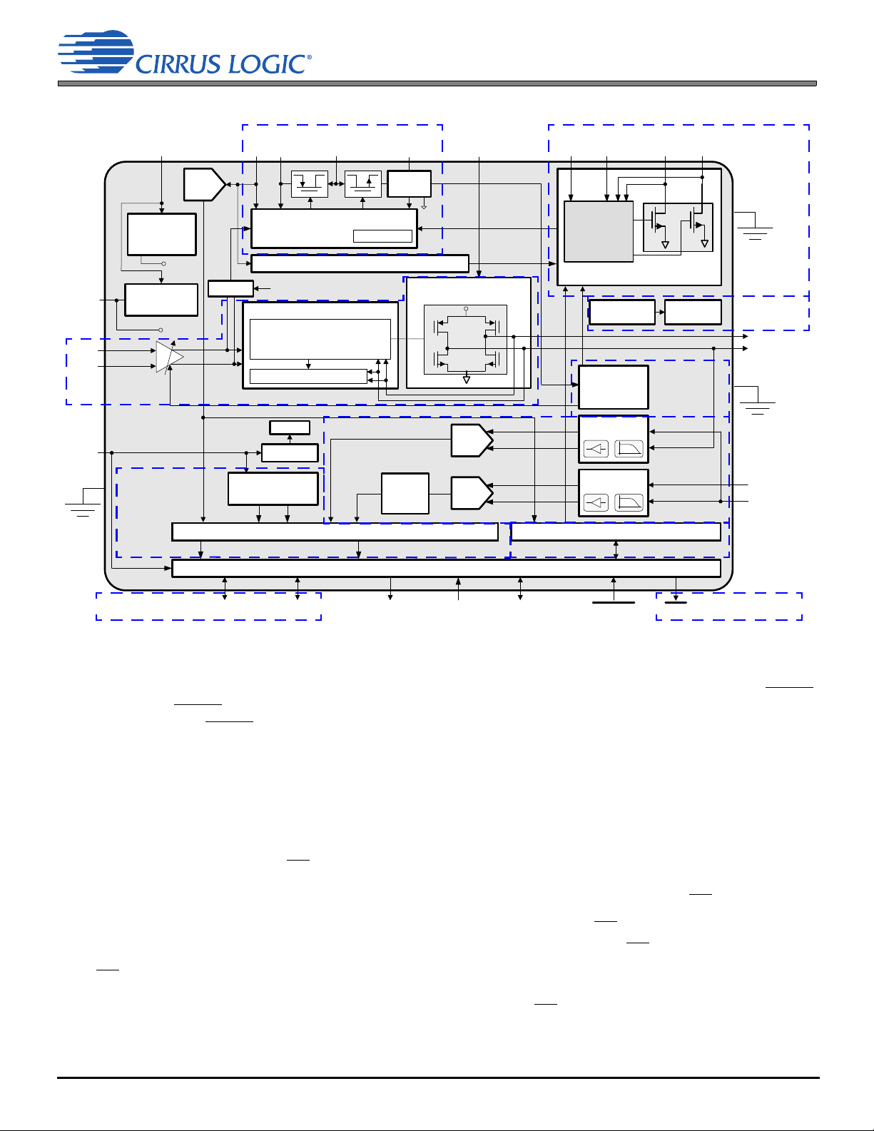
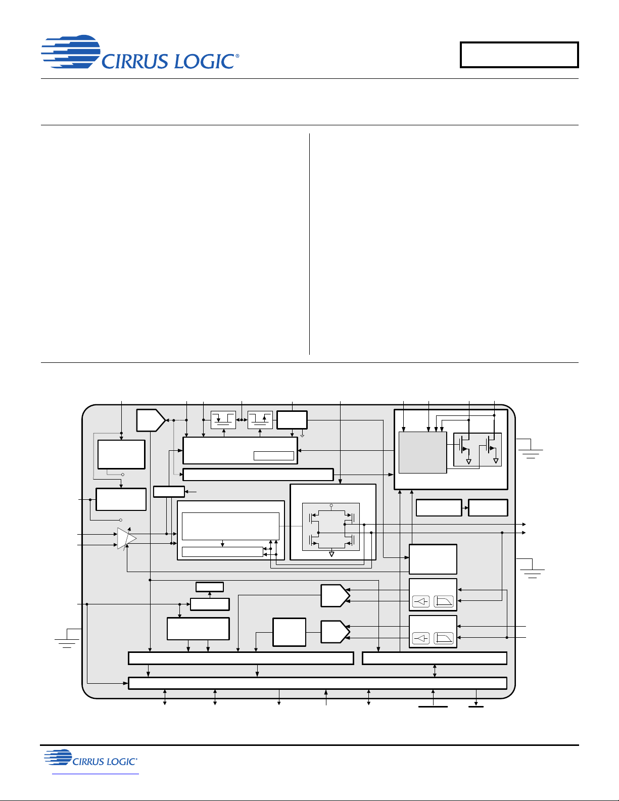
4 Functional Description
Class D Power Stage
SPKR SU PPLY
VP
GNDPLED
Current Mode Synchronous
Boost Controller
VCOM
Range
Scaling
Class D F r ont End
Short C ircuit Prot ection
∆Σ Class D M odulator
V
REF
Gener ation
Bandgap
Voltage
Gener ation
FILT+
VREF
ISENSE+
ISENSE–/
VSENSE+
SCLKLRC K
Soft Ramp
Level Shifters
I²C Control Port
SDASCLSCLK LRCK SDOUT
MCLK
IN–
–
+
9,12,15 , or
18 dB + Mute
IN+
Flash LED Current Driver
Control,
Sensing,
and Fault
Protection
FLOUT1 FLOUT2/AD0FLEN FLINH
SPKOUT+
SPKOUT–/
VSENSE–
I2C Class G Override
Watchdog
Error
GNDP
VSENSE–
VSENSE+
ISENSE–
ISENSE+
SPKR
SUPPLY
ADC
Serial Audio /Data Por t
Serial Port
Clock Generation
VA
RESET INT
VMON ADC
Front End
LP
IMON ADC
Front End
LP
Low Battery Management
Class G
VBST
Current
Sense
IREF+SW
Power
Budgeting
Temperature
Sensor
Overtemp
Protec tion
ADC
ADC
See Section 4.9 “LED Driver.”
See Section 4.4.
See
Section 4.11
“Audio/Data
Serial Port
(ADSP).”
See Section 4.8,
“Signal Monitoring.”
See
Section 4.10,
“Power
Budgeting.”
See
Section 4.7.
See Section 4.3.
See Section 4.6 “Boost Converter.”
See Section 4.11.
See Section 4.14.
See Section 4.2.
See Section 4.13,
“Device Clocking.”
CS35L32
4 Functional Description
4.1 Power Supplies
The VA and VP supplies are required for proper operation of the CS35L32. Before either supply is powered down, RESET
must be asserted. RESET
Timing requirement for RESET
generated internally (as described in Section 7.12) and connected to the high-power output stage of the Class D amplifier
through two balls: VBST and SPKRSUPPLY. By so doing, the speaker amplifier benefits from the proximity of the external
decoupling capacitor that is connected to the boosted supply.
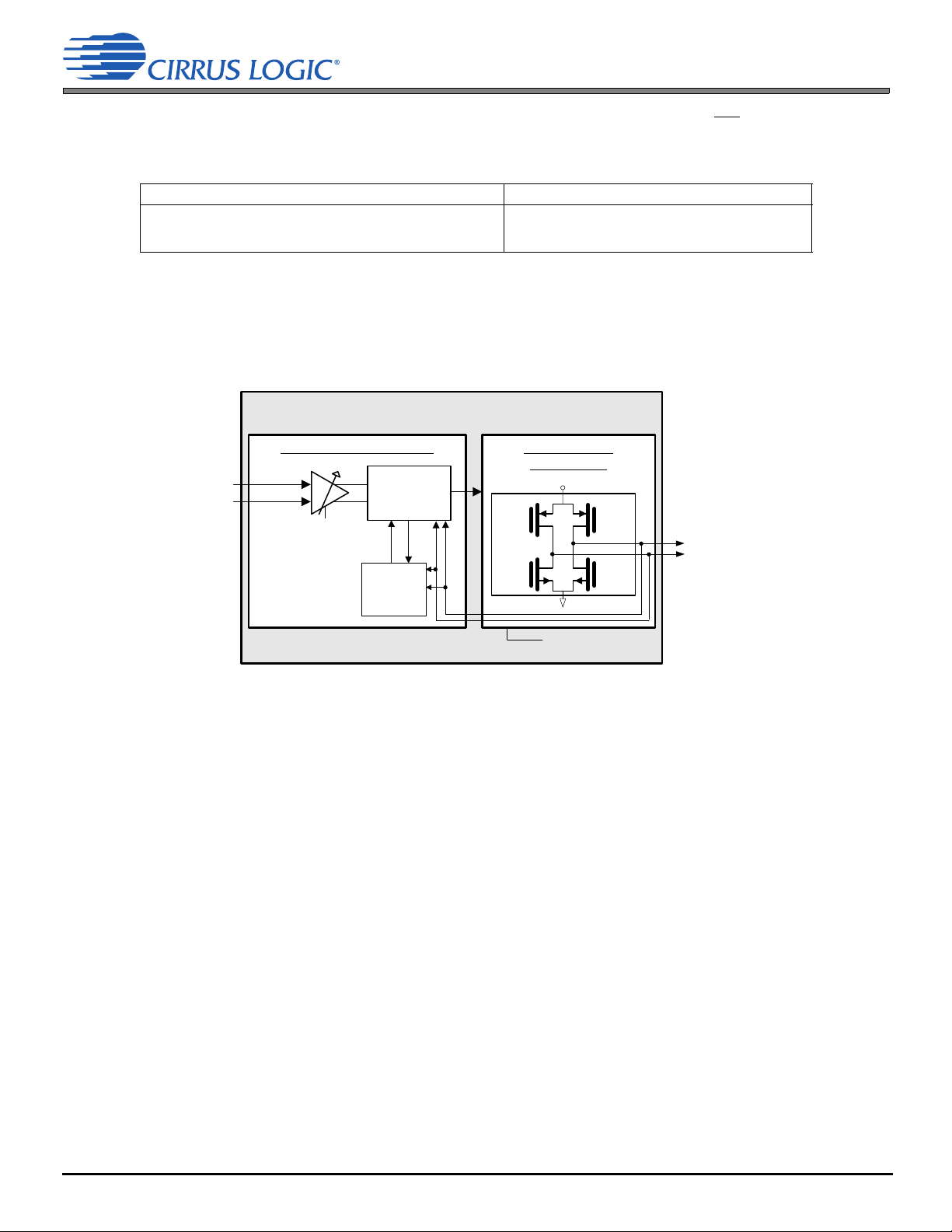
4.2 Interrupts
Events that require special attention, such as when a threshold is exceeded or an error occurs, are reported through the
assertion of the interrupt output pin, INT
individually masked by setting corresponding bits in the interrupt mask registers. Table 4-1 lists interrupt status and mask
registers. The configuration of mask bits determines which events cause the immediate assertion of INT
• When an unmasked interrupt status event is detected, the status bit is set and INT
• When a masked interrupt status event is detected, the interrupt status bit is set, but INT
Once INT
are sticky and read-to-clear: Once set, they remain set until the register is read and the associated interrupt condition is
not present. If a condition is still present and the status bit is read, although INT
is asserted, it remains asserted until all unmasked status bits that are set have been read. Interrupt status bits
must be held in the asserted state until all supplies are up and within the recommended range.
during supply power up and power down is described in Table 3-11. The VBST supply is
Figure 4-1. CS35L32 Block Diagram
. These events are captured within the interrupt status registers. Events can be
is deasserted, the status bit remains set.
is asserted.
:
is not affected.
DS963F4 15
Page 16
CS35L32
Hybrid Class D A udio Am plifier
(PDN_AMP = 0)
Hybrid Class D Modulator
-Class D
Modulator
9–18 dB
Short
Circuit
Protec tion
SPKOUT+
SPKOUT–
Hybrid Class D
Power Stage
VBST
IN+
IN–
AMP_GAIN p. 39
GAIN_CHG_ZC p. 39
AUDIOGAIN_MNG p. 38
V
IN1THOF
4
15
------ K
VBST
Gain
-----------------
=
V
IN1THON
2
3
---
K
VBST
Gain
-----------------
=
4.3 Speaker Amplifier
To clear any status bits set due to the initiation of a path or block, all interrupt status bits should be read after reset and
before normal operation begins. Otherwise, unmasking these previously set status bits causes INT
Table 4-1. Interrupt Status Registers and Corresponding Mask Registers
Status Registers Mask Registers
Interrupt Status 1 (Audio) (Section 7.19)
Interrupt Status 2 (Monitors) (Section 7.20)
Interrupt Status 3 (LEDs and Boost Converter) (Section 7.21)
Interrupt Mask 1 (Section 7.16)
Interrupt Mask 2 (Section 7.17)
Interrupt Mask 3 (Section 7.18)
4.3 Speaker Amplifier
The CS35L32 features a high-efficiency mono Class D audio amplifier, shown in Fig. 4-2, with an advanced closed-loop
architecture that achieves low levels of output distortion. Automatic Class G operation, using a boosted supply to the
amplifier, allows louder speaker performance with high crest factor.
to assert.
Figure 4-2. Speaker Amplifier Block Diagram
4.3.1 Class G Operation with LEDs Off
The boost converter output is the supply to the speaker amplifier. Audio operation can be programmed to have one of the
following supply modes (See Section 7.12 for programming details.):
• Class G where the boost converter is in Bypass Mode for audio input signals below a threshold V
5-V Boost Mode for audio signal inputs above a threshold V
IN1THOFF
. These thresholds are specified in Table 3-4
IN1THON
for the given conditions. The corresponding equations are shown below.
• Class G disabled, boost converter is in Bypass Mode, and VBST = VP. In this mode, thresholds are ignored.
• Class G disabled, boost converter is in Boost Mode, and VBST = 5 V. In this mode, thresholds are ignored.
The Class G equations for the audio input signal thresholds are as follows:
VBST is the boost converter output voltage (whether in Bypass or Boost Mode), and gain is audio gain expressed as a
unitless real ratio (nonlogarithmic). K = 1 if MCLK is 6 or 12 MHz; K = 1.024 if MCLK is 6.144 or 12.288 MHz. MCLK
should be configured as described in Section 4.13.1 and Section 7.7.
and
16 DS963F4
and in
INT
Page 17

CS35L32
4.4 Low-Battery Management
4.3.2 Class G Operation with LEDs On
If LEDs are active, the speaker amplifier supply in one of the following supply modes, as specified by VBOOST_MNG (see
Section 4.10.3 and Section 7.12 for details):
• Class G operation defaults to the higher supply setting: that requested by the LEDs or that requested by Class G.
The latter takes into account both thresholds V
IN1THOF
• Class G disabled and the speaker amplifier supply is set as requested by the LEDs. Thresholds are ignored.
• Class G disabled where the boost converter is in Bypass Mode (VBST = VP). Thresholds are ignored.
• Class G disabled where the boost converter is in Boost Mode and VBST = 5 V. Thresholds are ignored.
4.3.3 Error Conditions
Table 4-2 provides links to error status and mask bits for the Class D audio amplifier errors.
Table 4-2. Class D Audio Amplifier Error Status and Mask Bits
Error Cross-Reference to Description
Amplifier short/Amplifier short mask
Amplifier short release
Overtemperature error/Overtemperature error mask
Overtemperature error release
The CS35L32 monitors the OUT± terminals in real time to determine whether the output voltage signal correlates to the
PWM data stream driving the gate drivers internal to the device. If it is not, the CS35L32 interprets the discrepancy as a
short on the outputs, which may have been caused by a short to ground, across the speaker, or to the VBST rail.
AMP_SHORT p. 41, M_AMP_SHORT p. 40, also see Section 4.3.3
AMP_SHORT_RLS p. 39
OTE p. 41, M_OTE p. 40, also see Section 4.3.3
OTE_RLS p. 40
and V
IN1THON
, as described in Section 4.3.1.
If this error occurs, the AMP_SHORT status bit is set, and, if M_AMP_SHORT = 0, INT
is asserted. As a result, the device
enters Speaker-Safe Mode, which is described in Section 4.3.4.
The CS35L32 also enters Speaker-Safe Mode if its temperature exceeds the overtemperature shutdown threshold
specified in Table 3-3. The OTE status bit is set; if M_OTE = 0, INT
is asserted.
The amplifier shuts down automatically due to battery (VP) undervoltage, as described in Section 4.5. The amplifier
restarts automatically upon voltage recovery, with default gain.
The audio amplifier outputs are clamped to ground if MCLK stops, as described in Section 4.13.3.
4.3.4 Speaker-Safe Mode
Speaker-Safe Mode is entered according to the AMP_SHORT and OTE interrupt status bits as follows:
• In the event of an AMP_SHORT, the CS35L32 mutes the amplifier output to Hi-Z to protect the speaker while the
boost converter is allowed to operate normally.
• In the event of an OTE, the CS35L32 mutes the amplifier output to Hi-Z to protect the speaker and sets the boost
converter in Bypass Mode (VBST = VP). Normal behavior resumes when the error condition ceases and OTE_RLS
is sequenced as described in Section 4.7.1.
• If Speaker-Safe Mode is entered as a result of an AMP_SHORT error, normal behavior resumes when the short
condition ceases and the AMP_SHORT_RLS bit is sequenced as described in Section 7.15.
4.4 Low-Battery Management
Under heavy current loading, such as a high current LED flash event, the battery voltage drops. LOWBAT_TH (see p. 37)
allows the user to select a voltage threshold, below which flash current is reduced from the LED_FLCUR setting (see p. 43)
to the LED_FLINHCUR setting (see p. 44). Upon voltage recovery above LOWBAT_RECOV (see p. 37), the flash current
setting reverts to normal. The user should select a recovery threshold higher than the low-battery threshold.
Low-Battery Mode is entered only if a battery voltage falls below the programmed LOWBAT_TH during a flash event. This
condition is reported by the setting LOWBAT (see p. 42), which can be masked with M_LOWBAT (see p. 41).
INT
is deasserted after the interrupt registers are cleared by being read, provided the condition no longer exists.
DS963F4 17
Page 18

CS35L32
Boost Converter
VP VBST
VP SW
Rectifying FET
GND P
Boost C ontroller
2-MHz Clock
Set
Reset
Pulse
Width
Control
R
BST_SNS
IREF
GEN
V
BANDGAP
Internal
Reference
Circuitry
IREF+
C
BST(OUT)
C
BST(IN)
Boost
FET
L
BST
BST_IPK
on p. 38
Die Tempe rature Monitoring
Temperature
Sensor
VA
V
BANDGAP
Overtemperature Error Reference (TOP)
V
BANDGAP
Overtemperature Warning Reference (T
WRN
)
OTW on p. 41
M_OTW on p. 40
(see Section 4.7.1)
OTE on p. 41
M_OTE on p. 40
OTE_RLS on p. 40
(see Section 4.7.1)
4.5 Undervoltage Lockout (UVLO)
4.5 Undervoltage Lockout (UVLO)
If the VP level falls below the lockout threshold specified in Table 3-3, UVLO protection shuts down all analog circuitry of
the CS35L32. Autorecovery occurs as VP rises above the lockout threshold by a voltage equal to the specified hysteresis.
During a UVLO condition, control port, UVLO detection, serial clock, watchdog, and thermal detection circuitry stay active.
Note: During an UVLO condition, the I
2
S port is automatically powered down, preventing the UVLO condition from being
fed back via the ADSP SDOUT pin.
4.6 Boost Converter
The CS35L32's boost converter, shown in Fig. 4-3, delivers power to the supply of the audio speaker amplifier as well as
to the LEDs. Its output voltage is determined by VBOOST_MNG (see p. 38). Section 4.10 further shows how VBOOST_
MNG relates to audio and LED operation. The boost converter features a current-limiting circuit that detects and clamps
peak inductor current if such a peak is equal to the user-programmable limit (BST_IPK, see p. 38). BOOST_CURLIM
interrupt flag is set when the current limit has been detected.
MCLK
If MCLK
sets the frequency of the converter to 2 MHz. MCLK
INT
stops switching, the converter is placed in Bypass Mode until clocking is restored.
INT
is derived from MCLK by setting MCLKDIV2 (see p. 37).
INT
Figure 4-3. Boost Controller Block Diagram
4.7 Die Temperature Monitoring
Onboard die temperature monitoring prevents, shown in Fig. 4-4, the CS35L32 from reaching a temperature that would
compromise reliability or functionality. The CS35L32 incorporates a two-threshold thermal-monitoring system. When die
temperature exceeds the lower threshold, an overtemperature warning (OTW) event occurs; if it exceeds the second
threshold, an overtemperature error (OTE) condition occurs. These conditions are described in Section 4.7.1.
Note: The CS35L32 does not support independent powering down of die-temperature monitoring circuitry (other than
18 DS963F4
powering it down via PDN_ALL, see p. 36).
Figure 4-4. Die Temperature Monitoring
Page 19

CS35L32
Signal Monitoring
VSENSE+
Mult ibit
ADC
VSENSE–
ISENSE+
ISENSE–
Mult ibit
ADC
To Audio/
Data Serial
port
VP (3.0–5.25 V)
Mult ibit
ADC
Range Scaling
–30 to +36 dB
6-dB steps
VMON ADC F ront End
LP
IMON ADC Front End
LP
IMON_SCALE on p. 38
(PDN_xMON = 0)
4.8 Signal Monitoring
4.7.1 Error Conditions
Table 4-3 lists overtemperature error status and mask bits.
Table 4-3. Die Temperature Monitoring Configuration
Error Cross-Reference to Register Field Description
Overtemperature error/Overtemperature error mask
Overtemperature warning/Overtemperature warning mask
Overtemperature error release
The overtemperature error and warning error conditions are described in detail in the following:
• Overtemperature warning (OTW). An OTW event occurs when the die temperature exceeds the overtemperature
threshold (listed in Table 3-3). When this occurs, an OTW (see p. 41) event is registered in the interrupt status
(Section 7.19); if M_OTW = 0, INT
is asserted.
To exit the condition, the temperature must drop below the threshold and interrupt status 1 register must be read.
• Overtemperature error (OTE). An OTE event occurs when the die temperature exceeds the internally preset error
threshold (see Table 3-3). When this occurs, an OTE (see p. 41) event is registered in the interrupt status and, if
M_OTE =0, INT
is asserted. The CS35L32 shuts down, the Class D amplifier enters Speaker Safe Mode, as
described in Section 4.3.4, and the LED drivers shut down.
To exit, the temperature must drop below the overtemperature shutdown threshold and OTE_RLS must be
sequenced as described in Section 7.15. After OTE release, the amplifier and LED drivers recover to preshutdown
settings. The LED drivers must be retriggered with FLEN and/or FLINH inputs for a lighting event to occur.
OTE p. 41/M_OTE p. 40
OTW p. 41/M_OTW p. 40
OTE_RLS p. 40
4.8 Signal Monitoring
Signal-monitoring ADCs, shown in Fig. 4-5, give upstream system processors access to important signals entering and
exiting the device. The three monitoring signals are as follows:
An integrated ADC digitizes these analog signals, at which point, the audio/data serial port (ADSP) can send them to the
system processor.
4.8.1 Power-Up and Power-Down Bits (PDN_xMON)
The three ADCs can be powered down independently via their respective PDN_xMON bit in the control port, see
Section 7.6. To power down an ADC and its associated support circuitry, its PDN_xMON bit must be set; clearing PDN_
xMON powers up the corresponding circuitry.
Note: For proper operation, MCLK must be at the correct frequency (MCLK_ERR =0; see p. 41) and the device must
DS963F4 19
• VPMON: Monitors the voltage on the VP pin, which is most commonly the battery for the system.
• VMON: Monitors the output voltage of the Class D amplifier.
• IMON: Monitors the current that flows into the load being driven by the Class D amplifier.
Figure 4-5. Signal Monitoring Block Diagram (PDN_xMON = 0)
be powered (PDN_ALL = 0; see p. 36).
Page 20

CS35L32
VMON
D
OUT
2151–
-------------------
6.25 V A
1.8
--------------------------
=
IMON
D
OUT
2151–
-------------------
0.82 V A
0.1
--------------------------
=
4.8 Signal Monitoring
4.8.2 Monitoring Voltage across the Load—VMON
As shown in Fig. 4-5, monitoring on VMON is accomplished via the VSENSE± pins. Table 3-7 gives operating and
performance specifications for this ADC path. The following equation determines the VMON voltage (in Volts):
is the 16-bit digital output monitoring word in signed decimal format (–32,768 to +32,767) and VA is the voltage on
D
OUT
the VA pin. Relative to VSENSE+, negative D
equate to a positive load voltage. When VA is 1.8 V, the full-scale signal is 6.25 V.
If VMON is a 12-bit word, its equivalent 16-bit representation for the computational purposes of this section positions the
12 bits in the 12 MSBs and the 4 LSBs are cleared in the computation.
4.8.3 Monitoring Current through the Load—IMON
As shown in Fig. 4-5, monitoring of output current is accomplished via the ISENSE± pins, which are provided to measure
a voltage drop across a sense resistor in the output path, as described in Section 3. A precision resistor (1%) is chosen
for high accuracy when calculating the current from the voltage measured across the resistor. Likewise, to avoid thermal
drift, the resistor is chosen to have a low thermal coefficient of 100 ppm/°C. Table 3-7 gives operating and performance
specifications for this ADC path.
The following equation determines the IMON current (in Amps) when using a 0.1- sense resistor:
values equate to a negative load voltage and positive D
OUT
OUT
values
D
is the 16-bit digital output monitoring word in signed decimal format (–32,768 to +32,767) and VA is the voltage on
OUT
the VA pin. Relative to ISENSE+, negative D
values equate to a negative current and positive D
OUT
values equate to
OUT
a positive current. The default IMON_SCALE, as described in Section 4.8.3.1, is used for the example equation. If the
IMON_SCALE value is increased by 1 bit, the 2
value is decreased by 1 bit, the 2
15
power in the IMON equation decreases to 2
15
power in the IMON equation increases to 2
15–1
.
15+1
. If the IMON_SCALE
If IMON is a 12-bit word, its equivalent 16-bit representation for the computational purposes of this section positions the
12 bits in the 12 MSBs, and the 4 LSBs are cleared in the computation.
4.8.3.1 IMON Signal Scaling (IMON_SCALE)
Because the voltage is measured across a resistor of very small value and because output current can vary significantly
depending on the program material, a gain-scaling block (shown in Fig. 4-5) is included to improve the reported sample
resolution for low-level signals. This control, configured through IMON_SCALE (see p. 38), allows the system processor
to determine the range of bits to be received from the available 26-bit word on the IMON ADC’s data bus. The default
IMON_SCALE configuration (22 down to 7) configures the ADC data MSB (bit 22) to be the 16-bit IMON data packet MSB.
ADC bits 23–25 allow the signal to be divided down.
If IMON is a 12-bit word, its equivalent 16-bit representation for the computational purposes of this section positions the
12 bits in the 12 MSBs. The 4 LSBs are cleared in the computation.
4.8.3.2 IMON Sense Resistor
A 0.1-sense resistor is used to generate a differential voltage that is captured by the IMON circuitry to monitor the load
current. If PWM output filtering components, such as ferrite beads, are placed in series with the output load, the sense
resistor must be placed between the SPKOUT+ pin and the external series filter component, minimizing any performance
effects produced by the output filter. If the sense resistor is placed after the series-filtering component, the signal being
measured across the sense resistor will have been altered from its expected form.
20 DS963F4
Page 21

CS35L32
VP
D
OUT
128+
255
---------------------------------------
5
1
1.8
--------+
VA=
Flash LED Current Drivers
Control,
Sensing,
and Fault
Protection
FL OUT1 F LOUT2/AD0FLEN FLINH
I2C Control Port
Current Mode
Boost Controller
GNDPLED
LED_FLINHCUR
on p. 44
LED_FLCUR on p. 43
LED_MVCUR on p. 44
TIMER on p. 44
TIMEOUT_MODE on p. 44
4.9 LED Driver
4.8.4 Monitoring Voltage on the VP Pin—VPMON
Monitoring of the voltage present on the VP pin is integrated internally to the CS35L32. The operating specifications for
this ADC path are given in Table 3-7. To determine the voltage present on VP, the following equation must be used:
D
is the digital output word (see VPMON, p. 38) in signed decimal format (–128 to +127), and VA is the voltage on the
OUT
VA pin. If VA = 1.8 V, VPMON can report values from 2.8 V (D
4.8.5 Data Transmission out of the CS35L32
The ADSP, described in Section 4.11, can transmit all signals monitored in the CS35L32 to the system processor. The
data is presented on these outputs simultaneously.
4.8.6 Error Conditions
The CS35L32 monitors each monitoring ADC for overflow conditions. Table 4-4 lists signal monitoring error conditions and
provides links to their associated register field descriptions.
Table 4-4. Signal Monitoring Error Status Conditions
Error Cross-Reference to Description
xMON overflow. Indicates the overrange
status in the VMON, IMON, or VPMON
ADC signal paths.
If an overflow occurs, the appropriate xMON_OVFL bit is set, and, if the respective mask bit is cleared, an interrupt occurs.
Exiting the error occurs when the signal is no longer overflowing. No release bit needs to be toggled.
= –77 decimal) to 5.52 V (D
OUT
VMON_OVFL p. 42
IMON_OVFL p. 42
VPMON_OVFL p. 42
= 0 decimal).
OUT
4.9 LED Driver
The CS35L32 includes a high-current flash LED driver (see Fig. 4-6), featuring two channels, FLOUT1 and FLOUT2, and
a boost converter and current regulator designed to power LEDs with up to 0.75 A per channel. Both channels can be
combined to drive an LED with 1.5 A by tying FLOUT1 and FLOUT2 together.
• Overflow for VPMON and VMON signals. Due to the analog prescaling applied to the analog input signals, which
are sampled to make the VPMON and VMON signals, overflow conditions are unlikely on these ADCs. This is
because the operating specifications for maximum and minimum voltage constrain the voltage on these pins to a
level far below that required to make the ADC overflow.
For VPMON, because a spurious overflow error can occur when the block is taken out of power down, it is advised
to read the error status registers after PDN_xMON has been cleared to clear the spurious error status bit.
• Overflow for the IMON signal. As Section 4.8.3.1 describes, the IMON_SCALE (see p. 38) control allows the
greatest possible sample resolution over a wide range of output currents and sense resistors. If IMON_SCALE is
set too low for either the output current being monitored or the sense resistor being used, overflow of this ADC can
occur. When this error occurs, increasing the IMON_SCALE value can prevent the sampled signal from overflowing.
DS963F4 21
Figure 4-6. LED Driver Block Diagram
Page 22

CS35L32
t
flash
t
flash
FLASH
OFF
FLASH FLASH
Flash
Inhibit
FLASH
t
flash
FLASH
OFF OFF
OFFLED CURRENT
FLEN
FLINH
Flash Inhibit
(Timeout_Mode = 1)
Flash
Inhibit
t
flash
4.9 LED Driver
The CS35L32 is driven to flash when FLEN is asserted high. The I2C interface allows a host to program Flash and Movie
Mode currents, as well as a flash timer. The corresponding registers for these settings are LED_FLCUR (see p. 43), LED_
MVCUR (see p. 44), and TIMER (see p. 44). The flash event terminates at the end of a period determined by the flash
timer and optionally when FLEN is deasserted; this option is configured through TIMEOUT_MODE (see p. 44).
Flash current is reduced if FLINH is asserted. Currents in both channels are reduced to the LED_FLINHCUR setting (see
p. 44). If FLINH is deasserted, the current reverts to the LED_FLCUR setting, subject to the flash timer state.
Movie Mode operation has no timer and starts and ends according to the LED_MVCUR setting. Fig. 4-7 shows how Flash
and Flash Inhibit Mode currents are started and terminated.
To power the LED load, the LED driver and current regulator automatically boost the voltage if battery operation is
insufficient to produce the required LED currents. The controller bases whether to boost or operate in bypass, based on
maintaining a minimum voltage across the current regulator. The boost voltage varies by up to 5 V nominal, as described
in Section 4.10 and Section 7.12, depending on user selection.
Figure 4-7. LED Flash Timing Diagram
4.9.1 LED Driver Protection
The LED controller shuts down if the CS35L32’s temperature exceeds the overtemperature shutdown threshold specified
in Table 3-3. The OTE status bit is set and, and if M_OTE = 0, INT
is asserted. Recovery starts after the user clears OTE_
RLS (see p. 40), after which, the LED drivers must be retriggered with a FLEN signal for a flash event to occur, or with the
LEDx_MVEN enable bit (see Section 7.24) for a Movie Mode event to occur.
An automatic LED driver shutdown occurs in the event of a shorted or open LED. LED open and short conditions are
detected only when a Flash or Movie Mode event is initiated. For a Flash Mode event to occur after clearing the error status
bit, the LED drivers must be retriggered with a FLEN signal. For a Movie Mode event to occur after clearing the error status
bit, the LEDx_MVEN bit must be set.
4.9.2 LED Driver Interrupt
An interrupt is generated when any of the following conditions or faults occur: LEDx short or open is present when a Flash
event is initiated, current limit, boost output overvoltage, or UVLO of VP. The condition is registered in interrupt status
register 3, Section 7.21. Its mask is in Section 7.18. If the error conditions are no longer present, I
deasserted after the interrupt register is read.
Note: The device does not generate an LED open circuit interrupt if the boost converter is running in bypass mode
(PDN_BST= 01).
NT is reset and
22 DS963F4
Page 23

CS35L32
Flash LED
Current Drivers
IN–
–
+
IN+
Class D Amplifier
Overtemperature
Warning
Power Budgeting
Controller
Vds Monitor
Boost Drop
Current Limit
Boost Converter
OTW on p. 41
4.10 Power Budgeting
4.9.3 LED Lighting Status Register
The LED lighting status register (see Section 7.22) reports the state of LEDs and their controls. Status is reported for LED1
and LED2 flash events, indicating whether each LED is driven with current set by the flash setting. Likewise, status is
reported for LED1 and LED2 Movie Mode events, indicating whether each LED is driven with current set by the Movie
Mode setting. LED2 disable status is reported if FLOUT2 is used without an LED and is tied to ground, as shown in
Fig. 2-1. The logic status of the signal input at FLEN and FLINH is reported. Flash timer events are reported.
4.10 Power Budgeting
Power budgeting is configured through ILED_MNG, AUDIOGAIN_MNG, and VBOOST_MNG (see p. 38), which set the
boost converter’s output mode and the load management mode, as described in Section 4.10.1–Section 4.10.3. Load
management consists of reducing audio or LED load, or both, as long as one of the following conditions exists:
• The boost converter output voltage has dropped, provided that the boost converter is configured for a fixed 5-V
Mode through VBOOST_MNG and the load current has settled to its target value.
• The boost converter is in current limit.
• An overtemperature warning (135°C) has occurred.
Power budgeting is configurable to be active automatically without user intervention, semiautomatically, or
nonautomatically, where the user controls audio and LED load management.
Fig. 4-8 shows power budgeting.
4.10.1 Audio-Only Operation
If only audio is operating, there are no power-budgeting concerns. As a default, the boost converter’s output voltage is
fixed in Bypass Mode (VBST = VP). The user can set VBOOST_MNG (see p. 38) to any of the nondefault modes for a
different boost behavior. Refer to Section 4.3.1.
4.10.2 LED-Only Operation
If only LEDs are operating, the user can select one the following courses of action:
• By clearing ILED_MNG (see p. 38), LED current is managed automatically. If the CS35L32 enters load
• By setting ILED_MNG, the user maintains full control over LED current.
As a default, the boost converter’s output voltage is fixed in Bypass Mode (VBST = VP). The user can set VBOOST_MNG
to any of the nondefault modes for a different boost behavior. In particular, if VBOOST_MNG = 00 or 01 and load power
consists of LEDs only, the CS35L32 adapts for low power dissipation by automatically reducing the LED driver voltage
(Vds) at pins FLOUT1 and FLOUT2 and by reducing the boost converter’s output voltage. Such operation increases boost
converter efficiency, lowers temperature rise in the CS35L32, and increases battery run time. If VBOOST_MNG is set to
10 or 11, the CS35L32 does not adapt for low-power dissipation because the boost voltage is fixed.
DS963F4 23
Figure 4-8. Power Budgeting Block Diagram
management mode due to a condition listed in Section 4.10, the current is iteratively reduced until the condition no
longer exists.
Page 24

CS35L32
Level Shifter s
Audio Data Serial Port
From Signal
Monitoring Blocks
R
Onchip Channel
Select
LRCK SCLK
Onchip Serial Port
Rate Control
L
LRCK SCLK SDOUT
4.11 Audio/Data Serial Port (ADSP)
4.10.3 Audio and LED Operation
When audio and LEDs are operating simultaneously, the user can select one the following courses of action:
• By clearing AUDIOGAIN_MNG, if the CS35L32 enters load management mode due to the conditions listed in
Section 4.10, audio gain is reduced once by 3 dB (no reduction for 9-dB gain). If the condition persists, the CS35L32
examines ILED_MNG and responds according to Section 4.10.2. Audio automatically recovers to the original
volume after an LED event.
• By setting AUDIOGAIN_MNG, the user maintains full control over audio gain.
As a default, the boost converter’s output voltage is fixed in Bypass Mode (VBST = VP). The user can set VBOOST_MNG
to any of the nondefault modes for a different boost behavior. In particular, if VBOOST_MNG = 01 in the presence of LED
and audio load power, the CS35L32 adapts for low-power dissipation by automatically reducing the LED driver voltage at
pins FLOUT1 and FLOUT2 and by reducing the boost converter’s output voltage. If VBOOST_MNG = 00 in the presence
of LED and audio-load power, the boost converter’s output voltage is determined by the higher of the two supply
requirements for LED or audio Class G. In such a case, the CS35L32 cannot adapt for low power dissipation if audio
Class G requires a 5-V supply, because of the higher audio signal. Refer to Section 4.3.2.
4.11 Audio/Data Serial Port (ADSP)
The ADSP transmits audio and data to and from the systems processor in traditional I²S Mode. Controls are provided to
advise the device of the rate of the clocks being applied to its inputs when in Slave Mode. Likewise, the same controls are
used to indicate the clock rates to be generated when operating as a clock master.
The serial port I/O interface consists of three signals, described in detail in Table 1-1:
• SCLK: Serial data shift clock
• LRCK: Provides the left/right clock, which identifies the start of each serialized data word and toggles at sample rate
• SDOUT: Serial data output
Table 4-5 provides links to register fields used to configure components shown in Fig. 4-9.
.
4.11.1 Power Up, Power Down, and Tristate
The serial port has separate power-down and tristate controls for its output data path (SDOUT_3ST, see p. 37). ADSP
master/slave operation is governed only by the M/S setting (see p. 39), irrespective of the SDOUT_3ST setting. Table 4-6
describes ADSP operational mode and pin-output driver-state configuration.
Figure 4-9. Audio/Data Serial Port (ADSP)
Table 4-5. ADSP Configuration
Register Field Cross-Reference to Description
PDN_AMP
SDOUT_3ST
MCLKDIS, MCLKDIV2, RATIO
M/S
M_ADSPCLK_ERR
ADSPCLK_ERR
Section 7.5
Section 7.6
Section 7.7
Section 7.13
Section 7.16
Section 7.19
24 DS963F4
Page 25

CS35L32
4.11 Audio/Data Serial Port (ADSP)
Table 4-6. ADSP Operational Mode and Pin Configurations
M/S
SDOUT_3ST ADSP Operational Mode SDOUT Pin Driver LRCK Pin Driver SCLK Pin Driver
00I
01I
10I
11I
4.11.1.1 Tristating the ADSP SDOUT Path (SDOUT_3ST)
If the SDOUT functionality of the ADSP is not required, power losses caused by the charging and discharging of parasitic
capacitances on this pin can be eliminated by setting SDOUT_3ST, so that the SDOUT line is tristated. When reactivating
SDOUT, the associated circuits come alive and a full LRCK cycle elapses before SDOUT data is valid.
4.11.2 Master and Slave Timing
The serial port operates as either the master of timing or the slave to another device’s timing. When the serial port is
master, SCLK and LRCK are outputs; when it is a slave, they are inputs. Master/Slave Mode is configured by the M/S bit.
2
S Slave Mode Output Input Input
2
S Slave Mode Hi-Z Input Input
2
S Master Mode Output Output Output
2
S Master Mode Hi-Z Output Output
In I²S Master Mode, the SCLK and LRCK clock outputs are derived from MCLK
. SCLK is generated to have
INT
approximately 64 cycles per LRCK cycle.
In Slave Mode, because there is no sample-rate conversion from the serial port to the device core, the serial port audio
sample rate (f
serial port sample rate, the RATIO divider (see p. 37) is programmed to indicate the sample rate to MCLK
Table 4-7 shows the corresponding RATIO (f
Mode, in a dual-CS35L32 configuration (see Section 4.12.3) with MCLK
) must equal the core sample rate (Fs). To ensure that the CS35L32 maintains synchronization with the
LRCK
relationship.
INT
MCLK(INT)⁄fLRCK
) for each MCLK
INT
at the supported LRCK rate. In Master
INT
= 6 MHz, a ratio of 125 is not supported.
ADSPCLK_ERR (see p. 41) indicates when the ADSP attempts to resynchronize due to the absence of an LRCK edge at
the expected time due to excessive jitter, misprogramming, or clock absence. Note that, given that the clock-checking
circuit checks for LRCK edges appearing in the expected location relative to internal timing, if the LRCK frequency is an
integer multiple of the expected rate (e.g., the LRCK rate is 96 kHz [2 x 48 kHz] vs. the expected 48 kHz), ADSPCLK_ERR
does not detect this error condition. Also note that, since the clock-checking circuit monitors edges, if LRCK is removed
and no further clock edges are produced, ADSPCLK_ERR triggers only once while the LRCK is removed.
Table 4-7 lists supported serial-port audio sample rates, their relationship to the MCLK
rate, and the programming
INT
required to generate a given LRCK rate in Master Mode and ensure the serial port maintains synchronization in Slave
Mode.
Table 4-7. ADSP Rates
MCLK
Rate
INT
(MHz)
6.0000 48.000 125 1
6.1440 48.000 128 0
LRCK Rate
(kHz)
f
MCLK(INT)/fLRCK
(Rate Ratio)
RATIO
If all amplifier functionality is not being used, but CS35L32 clock mastering is desired, set up the clocks using the clocking
control register controls, then set SDOUT_3ST. In this scenario, since the amplifier is inaccessible, it should be powered
down to save power (PDN_AMP = 1).
4.11.3 ADSP in I2S Mode
The ADSP operates in traditional I²S format, with a minor modification. On the transmit side, the data structure is modified
to transmit nonconventional data (e.g., the monitored signals) in a compatible format. Receive Mode is not supported.
4.11.3.1 Data Bit Depths
The data word length of the I²S interface format is ambiguous. Fortunately, the I²S format is also left justified, with a MSBto-LSB bit ordering, which negates the need for a word-length control register. The following text describes how different
bit depths are handled with the I²S format.
DS963F4 25
Page 26

CS35L32
LRCK
SCLK
SDOUT
MSB MSB-1 LSB+1 LSB
1/Fs
ext
MSB MSB-1 LSB+1 LSB MSB
SCLK may
stop or continue
t
extraA =
None to some ti me
SCLK may
stop or continue
t
extraB =
None to some ti me
Left (A) Channel Right (B) Channel
4.12 Signaling Format
The CS35L32 transmits data that is from 24 to 32 bits deep per channel sample. If fewer than 24 serial clocks are present
per channel frame (half LR clock period), it outputs as many bits as there are clocks. If there are more than 24 serial clocks
per channel frame, it outputs the bits shown in the extended section for the additional clock cycles after the 24th bit. Any
bit beyond the 24th, if marked as reserved, is zero. The receiving device is expected to load the data in MSB-to-LSB order
until its word depth is reached, at which point it should discard any remaining LSBs from the interface.
4.12 Signaling Format
The CS35L32 supports the I²S format on its serial port:
• Up to 32 bits/channel of composite data can be sent, as shown in Table 4-9–Table 4-13. Additional bits are packed
in the extended section, beyond the 24th bit, and are accessed if a 32-clock frame is used.
• LRCK identifies the transmission start of each channel.
• Data is clocked out of the SDOUT output using the falling edge of SCLK.
• Bit order is MSB to LSB.
Signaling for I²S format is shown in Fig. 4-10.
Figure 4-10. I²S Format
4.12.1 Transmitting Data
The CS35L32 includes real-time monitoring of several signals internal and external to the device via integrated ADCs, as
well as a number of status bits. The monitoring data exists as three signals—VPMON, VMON, and IMON—which are
described in Section 4.8 and Table 4-8, which also describes status bits.
Table 4-8. SDOUT Monitor Data Description
Function Data Descriptor Description
Speaker
Amplifier
Section 4.3.
Undervoltage
Lockout (UVLO)
Section 4.5.
Boost Converter
Section 4.6.
Die
Temperature
Monitoring,
Section 4.7.
AMP_SHORT
(amplifier short)
UVLO
(UVLO event)
BOOST_CURLIM
(boost converter in
current limit)
BOOST_OVERROR
(boost converter
overvoltage error)
OTW
(overtemperature
warning)
OTE
(overtemperature
error)
Indicates that either of the outputs (OUT+ and/or OUT–) of the amplifier is driving a short circuit
0 (Default) Not shorted
1 Shorted. When this condition exists, the device enters Speaker-Safe Mode.
See Section 7.19 and Section 4.3.4.
0 (Default) No undervoltage lockout
1 UVLO detected at VP. IC shut down.
See Section 7.21.
0 (Default) Boost converter is not in current limit
1 Boost converter is in current limit
See Section 7.21.
0 (Default) No overvoltage detected
1 Overvoltage detected
See Section 7.21.
Indicates that device junction temperature exceeded the set limit in Table 3-3
0 (Default) Junction temperature is below the set overtemperature warning threshold
1 Junction temperature is above set overtemperature warning threshold
Indicates whether the device junction temperature exceeded the damage limit
0 (Default) Junction temperature is below damage limit
1 Junction Temperature is above damage limit. When this condition exists, the device enters
Speaker-Safe Mode.
See Section 7.19 and Section 4.3.4.
26 DS963F4
Page 27

Table 4-8. SDOUT Monitor Data Description (Cont.)
Function Data Descriptor Description
Signal
Monitoring,
Section 4.8.
LED Driver
Section 4.9.
Power down PDN_DONE
VMON_OVFL
(VMON overflow)
IMON_OVFL
(IMON overflow)
VPMON_OVFL
(VPMON overflow)
VMON
(voltage monitor)
IMON
(current monitor)
VPMON
(battery voltage)
LED12_FLEV
(LED12 flash event)
LED12_MVEV
(LED12 Movie Mode
event)
LED_TIMERON
(flash timer)
(power-down done)
xMON overflow. Indicates the overrange status in the VMON, IMON, or VPMON ADC signal path
0 (Default) No clipping has occurred anywhere in the ADC signal path.
1 Clipping has occurred in the ADC signal path.
The programming of IMON_SCALE may cause IMON_OVFL to be set. See Section 7.20.
16- or 12-bit representation of the voltage across the load, sensed on VSENSE±
16- or 12-bit representation of the voltage sensed across an external 0.1SPKOUT+ terminal, sensed on ISENSE±
8-bit representation of the voltage present on VP pin, i.e., the system’s battery voltage, sensed
internally
LED1 or LED2 flash event (Logical OR of LED1_FLEV and LED2_FLEV, see p. 43)
0 (Default) No driver flash current delivered to either LED1 or LED 2
1 Flash current delivered to LED1, LED2, or both
LED1 or LED2 movie event (Logical OR of LED1_MVEN and LED2_MVEV, see p. 43)
0 (Default) No driver movie current delivered to either LED1 or LED 2
1 Movie current delivered to LED1, LED2, or both
Flag indicating whether the flash timer is On. See Section 7.22.
0 (Default) LED Flash timer Off
1 LED Flash timer On
Indicates whether the CS35L32 is completely powered down and MCLK can be stopped. See
Section 7.20.
0 Not completely powered down. PDN_DONE = 0 if any blocks still require MCLK
powering down using PDN_ALL or the individual power-down bits, the CS35L32 transitions to a
powered-down state, after which, PDN_DONE is set and MCLK
1 (Default) Powered down
CS35L32
4.12 Signaling Format
resistor in series with the
. After
INT
can be removed.
INT
4.12.2 Transmitting Data from a Single-CS35L32 Configuration
For a single CS35L32, the user clears SHARE (see p. 39). When transmitting data via the ADSP, the monitor data is
packed as shown in Table 4-9: left channel VMON[15:0], VPMON[7:0] and right channel IMON[15:0], STATUS.
Table 4-9. SDOUT Monitor Data Positioning (Single CS35L32)
Bit Bit Number Left-Channel Data Contents Right-Channel Data Contents
MSB 1 VMON[15] IMON[15]
MSB – 1 2 VMON[14] IMON[14]
……… …
MSB – 15 16 VMON[0] IMON[0]
MSB – 16 17 VPMON[7] AMP_SHORT
MSB – 17 18 VPMON[6] OTW
MSB – 18 19 VPMON[5] OTE
MSB – 19 20 VPMON[4] VMONIMON_OVFL
MSB – 20 21 VPMON[3] VPMON_OVFL
MSB – 21 22 VPMON[2] PDN_DONE
MSB – 22 23 VPMON[1] BOOST_CURLIM
MSB – 23 24 VPMON[0] LED_TIMERON
MSB – 24 25 Reserved VMON_OVFL
MSB – 25 26 Reserved IMON_OVFL
MSB – 26 27 Reserved UVLO
MSB – 27 28 Reserved BOOST_OVERROR
MSB – 28 29 Reserved LED12_FLEV
MSB – 29 30 Reserved LED12_MVEV
MSB – 30 31 Reserved Reserved
MSB – 31 32 Reserved Reserved
DS963F4 27
Page 28

CS35L32
4.12 Signaling Format
4.12.3 Transmitting Data from a Dual-CS35L32 Configuration
To indicate a dual-CS35L32 configuration where the SDOUT line is shared, the user must set SHARE (see p. 39). When
two CS35L32 devices are available on the same board, each device is identified by its I
by FLOUT2. Upon power-up or upon deasserting RESET
, each CS35L32 reads the AD0 pin logic level and configures its
chip address. Transmission starts when SDOUT_3ST (see p. 37) is cleared. The Device 0 address (AD0 level low)
transmits its data on the left channel time slot while Device 1 is automatically tristated; the Device 1 address (AD0 level
high) transmits on the right-channel time slot while Device 0 is automatically tristated.
The DATCNF setting (see p. 39) determines data transmission for both CS35L32s, as shown below:
• Table 4-10 (DATCNF = 00): left and right channel VMON[11:0], IMON[11:0], VPMON[7:0]
• Table 4-11 (DATCNF = 01): left and right channel VMON[11:0], IMON[11:0], STATUS
• Table 4-12 (DATCNF = 10): left and right channel VMON[15:0], IMON[15:0]
• Table 4-13 (DATCNF): left and right channel VPMON[7:0], STATUS
Table 4-10. SDOUT Monitor Data Positioning (Two CS35L32s, DATCNF = 00)
Bit Bit Number Left-Channel Data Contents Right-Channel Data Contents
MSB 1 VMON[11] Device 0 VMON[11] Device 1
MSB – 1 2 VMON[10] Device 0 VMON[10] Device 1
……… …
MSB – 11 12 VMON[0] Device 0 VMON[0] Device 1
MSB – 12 13 IMON[11] Device 0 IMON[11] Device 1
MSB – 13 14 IMON[10] Device 0 IMON[10] Device 1
……… …
MSB – 23 24 IMON[0] Device 0 IMON[0] Device 1
MSB – 24 25 VPMON[7] Device 0 VPMON[7] Device 1
MSB – 25 26 VPMON[6] Device 0 VPMON[6] Device 1
……… …
MSB – 31 32 VPMON[0] Device 0 VPMON[0] Device 1
Table 4-11. SDOUT Monitor Data Positioning (Two CS35L32s, DATCNF = 01)
Bit Bit Number Left-Channel Data Contents Right-Channel Data Contents
MSB 1 VMON[11] Device 0 VMON[11] Device 1
MSB – 1 2 VMON[10] Device 0 VMON[10] Device 1
……… …
MSB – 11 12 VMON[0] Device 0 VMON[0] Device 1
MSB – 12 13 IMON[11] Device 0 IMON[11] Device 1
MSB – 13 14 IMON[10] Device 0 IMON[10] Device 1
……… …
MSB – 23 24 IMON[0] Device 0 IMON[0] Device 1
MSB – 24 25 AMP_SHORT Device 0 AMP_SHORT Device 1
MSB – 25 26 OTW Device 0 OTW Device 1
MSB – 26 27 OTE Device 0 OTE Device 1
MSB – 27 28 VMONIMON_OVFL Device 0 VMONIMON_OVFL Device 1
MSB – 28 29 VPMON_OVFL Device 0 VPMON_OVFL Device 1
MSB – 29 30 PDN_DONE Device 0 PDN_DONE Device 1
MSB – 30 31 BOOST_CURLIM Device 0 BOOST_CURLIM Device 1
MSB – 31 32 LED_TIMERON Device 0 LED_TIMERON Device 1
Table 4-12. SDOUT Monitor Data Positioning (Two CS35L32s, DATCNF = 10)
Bit Bit Number Left Channel Data Contents Right Channel Data Contents
MSB 1 VMON[15] Device 0 VMON[15] Device 1
MSB – 1 2 VMON[14] Device 0 VMON[14] Device 1
……… …
MSB – 15 16 VMON[0] Device 0 VMON[0] Device 1
MSB – 16 17 IMON[15] Device 0 IMON[15] Device 1
MSB – 17 18 IMON[14] Device 0 IMON[14] Device 1
……… …
MSB – 31 32 IMON[0] Device 0 IMON[0] Device 1
2
C address. The AD0 pin is shared
28 DS963F4
Page 29

Table 4-13. SDOUT Monitor Data Positioning (Two CS35L32s, DATCNF = 11)
Bit Bit Number Left Channel Data Contents Right Channel Data Contents
MSB 1 VPMON[7] Device 0 VPMON[7] Device 1
MSB – 1 2 VPMON[6] Device 0 VPMON[6] Device 1
……… …
MSB – 7 8 VPMON[0] Device 0 VPMON[0] Device 1
MSB – 8 9 AMP_SHORT Device 0 AMP_SHORT Device 1
MSB – 9 10 OTW Device 0 OTW Device 1
MSB – 10 11 OTE Device 0 OTE Device 1
MSB – 11 12 VMONIMON_OVFL Device 0 VMONIMON_OVFL Device 1
MSB – 12 13 VPMON_OVFL Device 0 VPMON_OVFL Device 1
MSB – 13 14 PDN_DONE Device 0 PDN_DONE Device 1
MSB – 14 15 BOOST_CURLIM Device 0 BOOST_CURLIM Device 1
MSB – 15 16 LED_TIMERON Device 0 LED_TIMERON Device 1
MSB – 16 17 VMON_OVFL Device 0 VMON_OVFL Device 1
MSB – 17 18 IMON_OVFL Device 0 IMON_OVFL Device 1
MSB – 18 19 UVLO Device 0 UVLO Device 1
MSB – 19 20 BOOST_OVERROR Device 0 BOOST_OVERROR Device 1
MSB – 20 21 LED12_FLEV Device 0 LED12_FLEV Device 1
MSB – 21 22 LED12_MVEV Device 0 LED12_MVEV Device 1
MSB – 22 to MSB – 31 23–32 Reserved Reserved
CS35L32
4.13 Device Clocking
4.13 Device Clocking
The device can operate as a clock master, creating both SCLK and LRCK for itself and for other devices in the system. It
can also be operated as a clock slave, receiving the SCLK and LRCK signals as input. In either case, internal controls are
used to advise (in Slave Mode) or set (in Master Mode) the clocking relationships among the externally applied MCLK, the
internally derived MCLK (MCLK
4.13.1 Internal Master Clock Generation
An internal clock (MCLK
MCLKDIV2 (see p. 37) so the proper internal MCLK signal can be derived. When the external clock is 6 or 6.144 MHz,
MCLK
can simply be a buffered version of the clock that drives the MCLK pin. This is done by clearing MCLKDIV2.
INT
However, if the external clock is 12 or 12.288 MHz, it must be halved to achieve an MCLK
This is done by setting MCLKDIV2.
Table 4-14 outlines the supported internal MCLK
frequencies of the external MCLK source (MCLK input pin).
To save power, MCLK can be disabled by setting MCLKDIS (see p. 37).
MCLK Rate (MHz) Required Divide Ratio MCLK
6.0000 1 6.0000 0
12.0000 2 1
6.1440 1 6.1440 0
12.2880 2 1
) is derived from the clocking signal that drives the MCLK pin. The user must configure
INT
), SCLK, and LRCK.
INT
Table 4-14. Internal Master Clock Generation
rate of approximately 6 MHz.
INT
nominal frequency and how it is derived from the supported
INT
Rate (MHz) Settings for MCLKDIV2
INT
4.13.2 ADSP Device Clocking
The CS35L32 can operate as a clock master, creating both SCLK and LRCK for itself and for other system devices. It can
also operate as a clock slave, receiving SCLK and LRCK signals as inputs. In Master Mode, CS35L32 determines clocking
relationships among SCLK, LRCK, and the externally applied MCLK.
DS963F4 29
Page 30

CS35L32
4.14 Control Port Operation
4.13.3 Error Conditions
MCLK, SCLK, and LRCK are monitored for clocking and configuration errors. If an MCLK or ADSP error occurs, the
respective MCLK_ERR or ADSPCLK_ERR bit is set, and, if the respective mask bit is cleared, INT
• MCLK error (MCLK_ERR). If MCLK were to stop abruptly while the boost converter or amplifier’s output stages are
switching, it could damage or destroy the device. Because of this, the CS35L32 integrates a watchdog circuit to
monitor MCLK frequency. To prevent damage, if MCLK is removed or drops below ~1.25 MHz, the boost converter
is placed in Bypass Mode and audio and LED operations are shut down. The Class D amplifier immediately stops
switching and both outputs are internally clamped to ground. After such a disturbance, once a proper MCLK can be
applied, the device should be reset to ensure recovery to a known state.
Whenever the MCLK watchdog determines that MCLK is too slow, the event is recorded in MCLK_ERR (see p. 41).
If MCLK_ERR is set, the device must be reset (RESET
HIGH) once a valid MCLK is reapplied, and then restarted adhering to the specifications in Table 3-11. Once
restarted, default audio functionality resumes with the boost converter in Bypass Mode. Registers must be reloaded,
since the RESET
• ADSPCLK error (ADSPCLK_ERR). If the ADSP RATIO is not configured properly for the MCLK and audio clocks
supplied to the CS35L32, an ADSP error is triggered (ADSPCLK_ERR = 1, see p. 41). Section 4.11.2 describes
ADSPCLK_ERR and how to configure the ADSP.
The CS35L32 monitors the MCLK
(see p. 37). If it is invalid, an ADSPCLK_ERR error occurs and, if M_ADSPCLK_ERR = 0, INT
While the ADSP is attempting to correlate the incoming clocks to the settings of the ratio controls, the state machine
may flag the error condition several times, causing multiple assertions of the INT
this error can be set after the initial notice, followed by the actions from a service routine to clear the error, and then
clearing the mask bit once the service routine has run.
This error is cleared automatically when the ratio matches the control port settings.
operation will have cleared them.
-to-LRCK ratio to determine whether it is valid according to the RATIO setting
INT
= HIGH LOW), released from reset (RESET = LOW
pin. To avoid this, the mask bit for
is asserted.
is asserted.
4.14 Control Port Operation
The control port is used to access the registers allowing the amplifier and LED drivers to be configured for the desired
operational modes and formats. Control port operation can be asynchronous with respect to the audio sample rates.
However, to avoid potential interference problems, the control-port pins should remain static if no operation is required.
The control port operates using an I²C interface with the amplifier acting as a slave device. Device communication should
not begin until the reset and power-up timing requirements specified in Table 3-11 and Table 3-13 are met.
Note: The VA and VP supplies are needed for proper control-port operation. Additionally, although registers can be
written to and read from while MCLK is powered down, a valid MCLK is required to advance the state machines
affected by register settings.
4.14.1 I²C Interface and Protocol
The serial control-port data pin, SDA, is a bidirectional data line. Data is clocked into and out of the CS35L32 by the I²C
clock, SCL. The signal timings for read and write cycles are shown in Fig. 4-11–Fig. 4-13. A start condition is defined as
a falling transition of SDA while the clock is high. A stop condition is defined as a rising transition of SDA while the clock
is high. All other SDA transitions occur while the clock is low.
The first byte sent to the CS35L32 after a start condition consists of a 7-bit chip address field and a R/W
read, low for a write) in the LSB. To communicate with the CS35L32, the I
match 100 0000 if the AD0 pin is at level 0, and should match 100 0001 if it is at level 1.
2
C slave address, shown in Fig. 4-11, should
bit (high for a
30 DS963F4
Page 31

CS35L32
4 5 6 7 24 25
SCL
CHIP ADDRESS (WRITE) MAP BYTE DATA
DATA
START
STOP
ACKACK
SDA
7 6 1 0
0 1 2 3 8 9 12 16 17 18 19 10 11 13 14 15 27 28
26
DATA
SDA
Source
Master Master Master
Pullup
Slave Slave Slave Slave
Master
Pullup
ACK
ACK
1 x x x x x x x
MAP Addr
INCR = 1
Slave Address
1 0 0 0 0 0 x 0
R/W = 0
Data to
Addr X+1
Data to
Addr X+n
Master Master
Slave
Data to
Addr X
7 6 1 0
7 6 1 0
AD0
SCL
DATA
STOP
ACK
ACK
SDA
7 0
7 0
CHIP ADDRESS (READ)
START
7 0
NO
258 9 184 5 6 7 0 1 2 3 16 17 34 35 36
ACK Slave Address
1 0 0 0 0 0 x 1
R/W = 1
DATA DATA
Data from
Addr X+n+1
Data from
Addr X+n+2
Data from
Addr X+n+3
SDA
Source
Master
Pullup
Slave S lave Slave
Master Master Master Pullup
27
AD0
SCL
CHIP ADDRESS (WRITE) MAP BYTE DATA
START
ACK
STOP
ACK
ACKACK
SDA
7 0 7 0
CHIP ADDRESS (READ)
START
1 x x x x x x x
7 0
NO
16 8 9 12 13 14 15 4 5 6 7 0 1 20 21 22 23 24
26 27 28
2 3 10 11 17 18 19 25
ACK
STOP
MAP Addr = Z
INCR = 1
Slave Address
1 0 0 0 0 0 x 0
R/W = 0
Slave Address
1 0 0 0 0 0 x 1
R/W = 1
DATA DATA
Data from
Addr Z
Data from
Addr Z+1
Data from
Addr Z+n
SDA
Source
Master Master Master
Pullup
Slave Slave
Slave Slave Slave
Master Master Master
Pullup
AD0
AD0
4.14 Control Port Operation
Figure 4-11. Control-Port Timing—I2C Writes with Autoincrement
The logic state of FLOUT2/AD0 configures the I²C device address upon a device power up, after RESET has been
deasserted. The bit labeled AD0 in the address byte in Fig. 4-11 reflects the logic state of pin FLOUT2/AD0.
If the I²C operation is a write, the next byte is the memory address pointer (MAP); the 7 LSBs of the MAP byte select the
address of the register to be read or written to next. The MSB of the MAP byte, INCR, selects whether autoincrementing
is to be used (INCR = 1), allowing successive reads or writes of consecutive registers.
Each byte is separated by an acknowledge bit, ACK, which the CS35L32 outputs after each input byte is read and is input
to the CS35L32 from the microcontroller after each transmitted byte.
Also for writes, bytes following the MAP byte are written to the CS35L32 register addresses pointed to by the last received
MAP address plus however many autoincrements have occurred. Fig. 4-11 shows a write pattern with autoincrementing.
If the operation is a read, the contents of the register pointed to by the last received MAP address plus however many
autoincrements have occurred, are output in the next byte. Fig. 4-12 shows a read pattern following the write pattern in
Fig. 4-11. Notice how read addresses are based on the MAP byte from Fig. 4-11.
Figure 4-12. Control-Port Timing—I²C Reads with AutoIncrement
If a read address different from that based on the last received MAP address is desired, an aborted write operation can
be used as a preamble that sets the desired read address. This preamble technique is shown in Fig. 4-11, in which a write
operation is aborted (after the ACK for the MAP byte) by sending a stop condition.
Figure 4-13. Control-Port Timing—I²C Reads with Preamble and Autoincrement
The following pseudocode illustrates an aborted write operation followed by a single read operation when the AD0 bit in
the slave address is 0. For multiple read operations, autoincrement would be set to ON (as shown in Fig. 4-13).
Send start condition.
Send 10000000 (chip address and write operation).
Receive acknowledge bit.
Send MAP byte, autoincrement off.
DS963F4 31
Page 32

CS35L32
5 Applications
Receive acknowledge bit.
Send stop condition, aborting write.
Send start condition.
Send 10000001 (chip address and read operation).
Receive acknowledge bit.
Receive byte, contents of selected register.
Send acknowledge bit.
Send stop condition.
Note: For I2C reads, the interrupt status registers and the register at the address that precedes an interrupt status
register must be read individually and not as a part of an autoincremented control-port read. An autoincremented
read of any of these registers may clear the contents of an interrupt status register and return invalid interrupt
status data. As a result, if an unmasked interrupt condition had caused the INT
autoincremented read that prematurely clears the corresponding interrupt status bit causes INT
pin to be asserted, the
to be deasserted.
Therefore, to avoid affecting interrupt status register contents, interrupt status registers and the register at the
preceding address (specifically, registers at addresses 0x14–0x17) must only be read individually.
5 Applications
5.1 RequiredReservedRegisterConfiguration
The following initialization sequence must be written after the release of reset but before power down bit is cleared:
• Write register 0x00 with the value 0x99.
• Write register 0x43 with the value 0x01.
• Write register 0x00 with the value 0x00.
To address the issue where a small dip can be seen in the audio output signal as the amplifier enters clipping, the following
2
I
C sequence must be written at initialization:
• Write register 0x00 with the value 0x99.
• Write register 0x3B with the value 0x62.
• Write register 0x3C with the value 0x80.
• Write register 0x00 with the value 0x00.
To address the issue where spurious tones exists on both the IMON/VMON ADCs during idle channel conditions, the
following I
2
C sequence must be written at initialization to reduce the amplitude of these tones:
• Write register 0x00 with the value 0x99.
• Write register 0x24 with the value 0x40.
• Write register 0x00 with the value 0x00.
By default, the boost converter output is incorrect if VP exceeds 3.7 V. When a boost event is requested in this condition,
the boost converter output is 5.8 V instead of the nominal 5 V.
The following I
2
C sequence must be written at initialization to correct this behavior:
• Write register 0x00 with the value 0x99.
• Write register 0x49 with the value 0x56.
• Write register 0x00 with the value 0x00.
5.2 Avoiding Current Transients when Issuing a Flash Event
When the boost converter is configured in either of the two automatic managed modes (VBOOST_MNG = 00 or VBOOST_
MNG = 01) and a flash LED event is indicated, a current transient can be seen at the output of the boost converter (VBST)
through FLOUTx whenever a voltage boost is requested. The duration of this transient is approximately 200 Did not
update. A current transient is also observed in the current that sources VP. The LED current settles to the programmed
value in the LED_FLCUR field after the current transient.
32 DS963F4
Page 33

CS35L32
Generic Simulated
Speaker Load
33 H
R
SENSE
0.1
8
SPKOUT+
ISENSE+
ISENSE –/VSENSE+
SPKOUT–/VSENSE–
FB
OUT
FB
OUT
SPK+
SPK–
C
OUT
C
OUT
5.3 External Component and PCB Design Considerations—EMI Output
To avoid the current transient on the VP node, the boost converter management must be configured for a fixed 5-V boost
operation (VBOOST_MNG = 11) before issuing a flash event. VBOOST_MNG may be reconfigured to the desired
management mode after a flash event.
The following sequence should be followed when issuing a flash event:
• Configure VBOOST_MNG to fixed 5-V Mode (VBOOST_MNG = 11).
• Trigger a flash event by asserting FLEN.
• Wait for the expiration of the flash timer period.
5.3 External Component and PCB Design Considerations—EMI Output Filtering
In a portable application, it is important not only to pass far-field radiated emissions compliance testing such as FCC
Part 15 or EN55022, but to minimize near-field emissions. In general, far-field compliance testing ensures that an
electronic device does not interfere with other electronic devices. Also, near-field emissions are more of a concern when
ensuring that an electronic device does not interfere with itself. As the name indicates, near-field emissions typically do
not propagate far enough to interfere with another device.
Depending on system characteristics (e.g., PCB layout, stack-up, supply decoupling, the connection length to the load,
presence of external shielding, sensitivity of other devices on the system, and proximity to any sensitive devices or
antennas), an EMI reduction may be necessary over the performance of what is obtained with the typical connection
diagram (see Fig. 2-1). Because most Class D amplifier emissions are produced or transmitted via the output stage,
changes are typically limited to adding passive filtering to SPKOUT+ and SPKOUT–. For sensitive systems, it is
recommended to add a ferrite-bead capacitor (FB-C) output filter to help ensure sufficient attenuation of the high-frequency
energy. Fig. 5-1 shows recommended VMON and IMON connections where an FB-C output filter is used.
5.4 PCB Routing Considerations for Thermal Relief
Due to the thermal dissipation properties inherent to a wafer-level chip scale package (WLCSP)—and because the
CS35L32 contains a boost converter, Class D amplifier, and LED driver, which can dissipate a fair amount of thermal
energy—the PCB design should account for how to remove heat from the device.
The simplest approach is to take advantage of as many GND ball locations as possible and connect them in a manner that
allows for good thermal conduction. For example, a 10-mil diameter, 6-mil drill through-hole microvia under each
nonblocking GND ball location would allow thermal energy to transmit through the PCB and reach the back-side surface,
where it dissipates most effectively. For reference purpose, GND balls are B5, C2, C3, C5, as shown in gray in Fig. 5-2.
DS963F4 33
Figure 5-1. VMON and IMON Connections with FB-C EMI Filtering
Page 34

CS35L32
Ball A1
Location
Indicator
5.5 Inductor Selection
Figure 5-2. Ground Ball Locations (Shown in Gray)
Also, as space permits, traces should be wider than 12 mils as soon as they clear the balls of the device. The traces should
remain wide for at least 300 mils after they leave the device.
5.5 Inductor Selection
Table 5-1, “Recommended Inductors,” lists the inductors recommended for use with the CS35L32.
Table 5-1. Recommended Inductors
Manufacturer Part Number Inductance DC Resistance Saturation Current
Cyntec PST031B-1R0MS 1.0 H 8.5 m 3.9 A 1.2 mm
Cooper MPI4040R1-1R0-R 1.0 H40
1.Indicates the inductor’s saturation current corresponding to a 30% drop in inductance from the nominal value.
m 7.7 A 1.2 mm
1
Height
34 DS963F4
Page 35

CS35L32
6 Register Quick Reference
6 Register Quick Reference
Default values are shown below the bit names.
AD0 = 0: 1000000[R/W
Adr. Function 7 6 5 4 3 2 1 0
Device ID A and B
0x01
(Read Only)
p. 36 00110101
Device ID C and D
0x02
(Read Only)
p. 36 10100011
Device ID E
0x03
(Read Only)
p. 36 00100000
0x04 Reserved —
Revision ID (Read
0x05
Only)
p. 36 xxxxxxxx
Power Control 1 PDN_AMP — PDN_BST[1:0] — PDN_ALL
0x06
p. 36 00000100
Power Control 2 PDN_VMON PDN_IMON PDN_VPMON — SDOUT_3ST —
0x07
p. 37 11101000
Clocking Control MCLKDIS MCLKDIV2 — RATIO
0x08
p. 37 01000000
Low Battery Thresholds — LOWBAT_TH[1:0] LOWBAT_RECOV[2:0] —
0x09
p. 37 00100110
Battery Voltage Monitor
0x0A
(Read Only)
p. 38 00000000
Boost Converter Peak
0x0B
Current Protection
Control
p. 38
Scaling — IMON_SCALE[3:0]
0x0C
p. 38 00000111
LED and Audio Power-
0x0D
Budget Management
p. 38 00000010
0x0E Reserved —
ADSP Control ADSP_DRIVE M/S DATCNF[1:0] SHARE —
0x0F
p. 39 00100000
Class D Amplifier
0x10
Control
p. 39 00010100
Protection Release
0x11
Control
p. 39 00000000
Interrupt Mask 1 — M_ADSPCLK_ERR M_MCLK_ERR M_AMP_SHORT M_OTW M_OTE
0x12
p. 40 11111111
Interrupt Mask 2 M_VMON_OVFL M_IMON_OVFL M_VPMON_OVFL — M_PDN_DONE
0x13
p. 40 11111111
Interrupt Mask 3 M_UVLO M_LED2_OPEN M_LED2_
0x14
p. 41 11111111
Interrupt Status 1
0x15
(Audio) (Read Only)
p. 41 xxxxxxxx
Interrupt Status 2
0x16
(Monitors) (Read Only)
p. 42 xxxxxxxx
Interrupt Status 3
0x17
(LEDs and Boost
Converter) (Read Only)
p. 42 xxxxxxxx
LED Lighting Status
0x18
(Read Only)
p. 43 xxxxxxxx
LED Flash Mode
0x19
Current
p. 43 00000000
LED Movie Mode
0x1A
Current
p. 44 00000000
LED Flash Timer — TIMER[4:0] TIMEOUT_MODE
0x1B
p. 44 00100100
LED Flash Inhibit
0x1C
Current
p. 44 00000000
0x1D
Reserved
–0x7F
] – 10000000 = 0x80 (Write); 10000001 = 0x81 (Read); AD0 = 1: 1000001[R/W] – 10000010 = 0x82 (Write); 10000011 = 0x83 (Read)
DEVIDA[3:0] DEVIDB[3:0]
DEVIDC[3:0] DEVIDD[3:0]
DEVIDE[3:0]
00000000
AREVID[3:0] NUMREVID[3:0]
01000000
—ILED_MNGAUDIOGAIN_MNG — VBOOST_MNG[1:0]
xxxxxxxx
— AMP_GAIN[2:0] GAIN_CHG_ZC —
— ADSPCLK_ERR MCLK_ERR AMP_SHORT OTW OTE
VMON_OVFL IMON_OVFL VPMON_OVFL — PDN_DONE
UVLO LED2_OPEN LED2_SHORT LED1_OPEN LED1_SHORT LOWBAT BOOST_
LED1_FLEV LED2_FLEV LED1_MVEV LED2_MVEV LED_FLEN LED_FLINH LED2_DIS LED_TIMERON
— LED_FLCUR[3:0]
— LED_MVCUR[2:0] — LED1_MVEN LED2_MVEN
— LED_FLINHCUR[3:0]
xxxxxxxx
I²C Address:
—
VPMON[7:0]
BST_IPK[7:0]
— AMP_SHORT_RLS — OTE_RLS
SHORT
M_LED1_OPEN M_LED1_
SHORT
—
M_LOWBAT M_BOOST_
CURLIM
CURLIM
M_BOOST_
OVERROR
BOOST_
OVERROR
DS963F4 35
Page 36
CS35L32
7 Register Descriptions
7 Register Descriptions
All registers are read/write except for the chip ID and revision register and the status registers, which are read only. The
user must not change reserved registers from their default state.
7.1 Device ID A and B
R/O
Default00110101
76543210
DEVIDA[3:0] DEVIDB[3:0]
7.2 Device ID C and D
R/O
Default10100011
76543210
DEVIDC[3:0] DEVIDD[3:0]
7.3 Device ID E
R/O
Default00100000
76543210
DEVIDE[3:0] —
Address 0x01
Address 0x02
Address 0x03
Bits Name Description
7:4 DEVIDA,
DEVIDC,
DEVIDE
3:0 DEVIDB,
DEVIDD
7.4 Revision ID
R/O
Defaultxxxxxxxx
Device ID code for the CS35L32.
DEVIDA 0x3
DEVIDB 0x5
DEVIDC 0xA Represents the “L” in CS35L32
DEVIDD 0x3
DEVIDE 0x2
76543210
AREVID[3:0] NUMREVID[3:0]
.
Address 0x05
Bits Name Description
7:4 AREVID Alpha revision. AREVID and NUMREVID form the complete device revision ID (e.g., A0, B2).
3:0 NUMREVID Numerical revision. AREVID and NUMREVID form the complete device revision ID (e.g., A0, B2).
7.5 Power Control 1
R/W
PDN_AMP — PDN_BST[1:0] — PDN_ALL
Default00000100
Bits Name Description
7 PDN_
AMP
6:4 — Reserved
3:2 Power-down boost converter. Configures the power state of the boost converter.
1—Reserved
0PDN_
ALL
0xA A … 0xF F
0x0 0 … 0xF F
Address 0x06
76543210
Power down Class D amplifier. Configures the power state of the Class D amplifier.
0 (Default) Powered up
1 Powered down
00 Powered up
01 (Default) Boost Mode bypass. Turns the boost FET OFF, the rectifying FET ON, and the remaining boost circuitry in a low-
power state, with VBST = VP. Powers down internal-control circuitry when operating in VBST = VP Mode.
10–11 Reserved
Power down all. Configures the CS35L32 power state. Can be used to quickly power down the device but is not equivalent to
using all of the individual power-down bits.
0 (Default) Powered up, as per individual controls in power control registers 1 and 2.
1 Powered down. All affected blocks are powered down, regardless of individual power-down bit settings.
36 DS963F4
Page 37

CS35L32
7.6 Power Control 2
7.6 Power Control 2
R/W
Default11101000
Bits Name Description
7PDN_
VMON
6PDN_
5PDN_
VPMON
4—Reserved
3 SDOUT_
2:0 — Reserved
76543210
PDN_VMON PDN_IMON PDN_VPMON — SDOUT_3ST —
Power-down VMON ADC. Configures the power state of the ADC front end and the ADC used to monitor the VSENSE± input
pins to create the VMON data.
0 Powered up
1 (Default) Powered down
IMON
Power-down IMON ADC. Configures the power state of the ADC front end, and the ADC, and range selection circuitry used to
monitor the ISENSE± input pins to create the IMON data.
0 Powered up
1 (Default) Powered down
Power-down VPMON ADC. Configures the ADC front end power state and the ADC used to monitor the VP supply pin to create
the VP data.
0 Powered up
1 (Default) Powered down
Tristate the ADSP SDOUT path. Configures the Hi-Z state of the ADSP SDOUT output path.
3ST
0 SDOUT is powered up.
1 (Default) SDOUT is Hi-Z.
7.7 Clocking Control
R/W
Default01000000
Because clock rates must be stable when the device is powered up, the device must be powered down before changing clock rates.
Bits Name Description
7 MCLKDIS MCLK disable. Configures the state of MCLK
6 MCLKDIV2 MCLK divide by 2. Configures a divide between the input pin MCLK and the derived core clock, MCLK
5:1 — Reserved
0RATIO
76543210
MCLKDIS MCLKDIV2 — RATIO
before its fan-out to all the internal circuitry.
0 (Default) On
1 Off. Disables the clock tree to save power when the device is powered down. Set only after the device powers down.
0 No divide
1 (Default) Divide by 2
f
MCLK(INT)/fLRCK
0 (Default)128
1 125
Application: Refer to Section 4.11.2, “Master and Slave Timing.”
ratio. Ta bl e 3 - 12 shows the effect of these settings on the Master Mode duty cycle.
INT
7.8 Low Battery Thresholds
R/W
Default00100110
76543210
— LOWBAT_TH[1:0] LOWBAT_RECOV[2:0] —
Address 0x07
Address 0x08
.
INT
Address 0x09
Bits Name Description
7:6 — Reserved
5:4 LOWBAT_THLow battery nominal threshold, falling VP. See Ta bl e 3 - 3 for accuracy specifications.
00 3.1 V 01 3.2 V 10 (Default) 3.3 V 11 3.4 V
3:1 LOWBAT_
RECOV
0—Reserved.
Low battery nominal recovery threshold, rising VP. See Ta bl e 3 - 3 for accuracy specifications.
000 Reserved
001 3.2 V
010 3.3 V
011 (Default) 3.4 V
100 3.5 V
101 3.6 V
110–111 3.6 V
DS963F4 37
Page 38

CS35L32
7.9 Battery Voltage Monitor
7.9 Battery Voltage Monitor
R/O
Default00000000
Bits Name Description
7:0 VPMON Battery voltage (VP) monitor. Represents the VPMON (D
76543210
VPMON[7:0]
) value in the equation in Section 4.8.4.
1000 0000 –128
1000 0001 –127…
1111 1111 –1
0000 0000 0 (default)
OUT
0000 0001 +1
0000 0010 +2 …
0111 1111 +127
7.10 Boost Converter Peak Current Protection Control
R/W
Default01000000
Bits Name Description
7:0 BST_IPK Boost converter peak current limit (A). Configures the peak current limit on the boost converter’s output. If the amplifier or LEDs
76543210
BST_IPK[7:0]
attempt to draw current above this limit, only the set limit current is provided and, consequently, the boost voltage droops. The
user must not write values higher than 0x80 to this register.
0000 0000 2.89 …
0010 0000 3.30 …
0100 0000 (Default) 3.72 …
0110 0000 4.14 …
1000 0000 4.56
1000 0001–1111 1111 Reserved
7.11 Scaling
R/W
Default00000111
76543210
— IMON_SCALE[3:0]
Address 0x0A
Address 0x0B
Address 0x0C
Bits Name Description
7:4 — Reserved
3:0 IMON_
SCALE
7.12 LED and Audio Power-Budget Management
R/W
Default0000 0 010
Bits Name Description
7:5 — Reserved
4 ILED_MNG LED current management
3 AUDIOGAIN_
2—Reserved
1:0 VBOOST_
Select IMON ADC scaling. Configures the scaling of data bits from the ADC to be output from the ADSP as the IMON data
word. The scale is selected from the encoded ADC output data bus with bit 22 being the ADC data MSB. Scaling control can
be used to improve the reported sample resolution for low-level signals or to divide down the signal.
0000 15 down to 0
…
Note: For 12-bit implementations, IMON_SCALE remains the same. The MSB is in the same place for 12- and 16-bit formats,
7654 3 210
— ILED_MNG AUDIOGAIN_MNG — VBOOST_MNG[1:0]
0 (Default) Automatically reduce LED current, only to avoid thermal shutdown or current limiting the boost converter.
1 User controls LED current (nonautomatic).
MNG
MNG
Audio-gain management when LEDs are active.
0 (Default) Automatically reduces audio volume once by 3 dB, only if needed to avoid thermal shutdown or current
limiting the boost converter. If the condition persists, the CS35L32 examines ILED_MNG and responds accordingly.
Audio recovers to original volume automatically at the end of the LED event.
1 User controls audio volume (nonautomatic).
Boost voltage control.
00 Automatically managed. Boost-converter output voltage is the higher of the two: Class G or adaptive LED voltage.
01 Automatically managed irrespective of audio, adapting for low-power dissipation when LEDs are ON, and operating
in Fixed-Boost Bypass Mode if LEDs are OFF (VBST = VP).
10 (Default) Boost voltage fixed in Bypass Mode (VBST = VP).
11 Boost voltage fixed at 5 V.
0111 (Default) 22 down to 7
1000 23 down to 8
1001 24 down to 9
1010 25 down to 10
1011–1111 Reserved
Address 0x0D
38 DS963F4
Page 39

CS35L32
7.13 ADSP Control
7.13 ADSP Control
R/W
Default00100000
Bits Name Description
7ADSP_
DRIVE
6 M/S ADSP Master/Slave Mode. Configures the ADSP I/O clocking. See Section 4.11.2 for details.
5:4 DATCNF Data configuration for dual CS35L32 applications only. Determines the data packed in a two-CS35L32 configuration.
3 SHARE SDOUT sharing. Determines whether one or two CS35L32 devices are on board sharing SDOUT.
2:0 — Reserved
76543210
ADSP_DRIVE M/S DATCNF[1:0] SHARE —
ADSP output drive strength. Selects the drive strength used for the ADSP outputs. These outputs include SDOUT as well as
SCLK and LRCK when the device is in Master Mode. Table 3-8 lists drive-strength specifications.
0 (Default) 1x
10.5x
0 (Default) Slave (SCLK/LRCK input only)
1 Master (SCLK/LRCK output only)
00 Left/right channels VMON[11:0], IMON[11:0], VPMON[7:0]. See Table 4-10.
01 Left/right channels VMON[11:0], IMON[11:0], STATUS. See Table 4-11.
10 (Default) left/right channels VMON[15:0], IMON [15:0]. See Table 4-12.
11 Left/right channels VPMON[7:0], STATUS. See Table 4-13.
0 (Default) One IC. Data configuration per Table 4-9.
1 Two ICs. For data configuration, refer to DATCNF (bits 5:4. above).
7.14 Class D Amplifier Control
R/W
Default00010100
76543210
— AMP_GAIN[2:0] GAIN_CHG_ZC —
Address 0x0F
Address 0x10
Bits Name Description
7:6 — Reserved
5:3 AMP_GAIN Amplifier gain. Configures the amplifier gain. Step size: ~3 dB
000 Mute (–80 dB)
001 9 dB
2GAIN_
CHG_ZC
1:0 — Reserved
Gain change zero-cross. Configures when AMP_GAIN (see p. 39) changes are applied.
0 Changes are not aligned to zero crosses.
1
(Default) Changes are delayed to occur at zero crossings
7.15 Protection Release Control
R/W
Default 0 0 0 0 0 0 0 0
Bits Name Description
7:3 — Reserved
2AMP_
SHORT_
1—Reserved
7654 3 2 1 0
Amplifier short protection release. Releases amplifier short protection that places the device into Speaker-Safe Mode if the
RLS
amplifier short condition is no longer present, which can be determined by reading AMP_SHORT (see Section 7.19) twice.
0 (Default)
1
0 1 0 sequence
010 (Default) 12 dB
011 15 dB
— AMP_SHORT_RLS — OTE_RLS
If the amplifier short condition is present, Speaker-Safe Mode is applied.
After the sequence, if the short condition is no longer present, Speaker-Safe Mode is cleared unless
an OTE condition is active. During the sequence, short monitoring is inactive because the amplifier is
in an OFF state, as explained in Section 7.19. Short monitoring resumes after the sequence.
100 18 dB
101–111 Reserved
Address 0x11
DS963F4 39
Page 40

CS35L32
7.16 Interrupt Mask 1
Bits Name Description
0OTE_
RLS
Note: For these bits, if the condition that causes automatic protection becomes true again during the protection potential release sequence
(x_RLS: 0 1 0), protection is not removed, the related interrupt status bit is set again, and, if unmasked, a new interrupt is generated.
Overtemperature error protection release. Releases (removes) OTE-caused Speaker-Safe Mode if the OTE condition is no
longer present, which can be determined by reading OTE (see Section 7.19) twice.
0 (Default)
1
0 1 0 sequence
If the OTE condition is present, Speaker-Safe Mode is applied.
At the end of the sequence, if the OTE condition is no longer present, the Speaker-Safe Mode is
cleared, unless an amplifier short cause is still active.
7.16 Interrupt Mask 1
R/W
Default 1 1 1 1 1 1 1 1
Interrupt mask register bits serve as a mask for the interrupt sources in the interrupt status registers. Interrupts are described in Section 4.2.
Bits Name Description
7:5 — Reserved
4 M_ADSPCLK_ERR Error masks
3 M_MCLK_ERR
2 M_AMP_SHORT AMP_SHORT mask
1M_OTWOTW mask
0M_OTEOTE mask
765 4 3 2 1 0
— M_ADSPCLK_ERR M_MCLK_ERR M_AMP_SHORT M_OTW M_OTE
0 Unmasked
1 (Default) Masked
0 Unmasked
1 (Default) Masked
0 Unmasked
1 (Default) Masked
0 Unmasked
1 (Default) Masked
7.17 Interrupt Mask 2
R/W
Default1 1 1 1111 1
Interrupt mask register bits serve as a mask for the interrupt sources in the interrupt status registers. Interrupts are described in Section 4.2.
76 543210
M_VMON_OVFL M_IMON_OVFL M_VPMON_OVFL — M_PDN_DONE
Address 0x12
Address 0x13
Bits Name Description
7 M_VMON_OVFL Overflow masks
6M_IMON_OVFL
5 M_VPMON_OVFL
4:1 — Reserved
0 M_PDN_DONE PDN_DONE mask
0 Unmasked
1 (Default) Masked
0 Unmasked
1 (Default) Masked
40 DS963F4
Page 41

CS35L32
7.18 Interrupt Mask 3
7.18 Interrupt Mask 3
R/W
Default 1 1 1 1 1 1 1 1
Interrupt mask register bits serve as a mask for the interrupt sources in the interrupt status registers. Interrupts are described in Section 4.2.
Registers at addresses 0x14–0x17 must not be part of a control-port autoincremented read and must be read individually. See Section 4.14.1.
Bits Name Description
7 M_UVLO UVLO mask
6 M_LED2_OPEN LED 2/1 open and shorted masks
5 M_LED2_SHORT
4 M_LED1_OPEN
3 M_LED1_SHORT
2 M_LOWBAT Low battery mask
1 M_BOOST_CURLIM Boost converter masks
0 M_BOOST_OVERROR
76 5 4 3 2 1 0
M_UVLO
M_LED2_OPEN M_LED2_SHORT M_LED1_OPEN M_LED1_SHORT
0 Unmasked
1 (Default) Masked
0 Unmasked
1 (Default) Masked
0 Unmasked
1 (Default) Masked
0 Unmasked
1 (Default) Masked
M_LOWBAT M_BOOST_CURLIM M_BOOST_OVERROR
7.19 Interrupt Status 1 (Audio)
R/O
Default x x x x x x x x
Interrupt mask register bits serve as a mask for the interrupt sources in the interrupt status registers. Interrupts are described in Section 4.2.
Registers at addresses 0x14–0x17 must not be part of a control-port autoincremented read and must be read individually. See Section 4.14.1.
76543210
— ADSPCLK_ERR MCLK_ERR AMP_SHORT OTW OTE
Address 0x14
Address 0x15
Bits Name Description
7:5 — Reserved
4ADSPCLK_
ERR
3MCLK_
ERR
2AMP_
SHORT
1 OTW Overtemperature warning. Indicates that device junction temperature exceeded the set limit, as described in Tab l e 3 -3 .
0 OTE Overtemperature error. Indicates whether the device junction temperature exceeded the damage limit.
ADSP clock error. Indicates that the ADSP has lost synchronization. See Section 4.11.2 and Section 7.7 for details.
0 (Default) MCLK
1MCLK
Master clock error. Indicates the MCLK watchdog status.
0 (Default) MCLK is above ~1.25 MHz.
1 MCLK is below ~1.25 MHz, so the device should be reset (RESET
LOW HIGH) when a valid MCLK is reapplied, and restarted. If this condition exists, the Class D amplifier
immediately stops switching and the outputs are internally clamped to ground
Amplifier short. Indicates that either of the amplifier outputs (OUT±) is driving a short circuit.
0 (Default) Not shorted
1 Shorted. The device enters Speaker-Safe Mode (see Section 4.3.4). Normal behavior may resume when the short
condition ceases and AMP_SHORT_RLS is sequenced, as described in Section 7.15.
Note: The circuit feeding this bit requires the amplifier to be fully powered and not in shut-down mode; if it is powered down
(PDN_AMP = 1) or in Speaker-Safe Mode, the detector indicates no short condition, even if speaker outputs are shorted.
0 (Default) Below set overtemperature warning threshold
1 Above set overtemperature warning threshold
0 (Default) Below damage limit
1 Above damage limit. The device enters Speaker-Safe Mode (see Section 4.3.4). Normal behavior may resume when
the OTE event ends and OTE_RLS is sequenced, as described in Section 7.15.
-to-LRCK ratio is invalid. Set as the ADSP resynchronizes on initial power up and application of clocks.
INT
-to-LRCK ratio is valid. Valid if f
INT
LRCK
=f
MCLK(INT)
/RATIO
= HIGH LOW), released from reset (RESET =
. See Section 4.13.3.
DS963F4 41
Page 42

CS35L32
7.20 Interrupt Status 2 (Monitors)
7.20 Interrupt Status 2 (Monitors)
R/O
Defaultxxxxxxxx
Interrupt status bits are read only and sticky. Interrupts are described in Section 4.2. Registers at addresses 0x14–0x17 must not be part of a
control-port autoincremented read and must be read individually. See Section 4.14.1.
Bits Name Description
7 VMON_OVFL xMON overflow. Indicates the overrange status in the VMON, IMON, or VPMON ADC signal path
6IMON_OVFL
5 VPMON_OVFL
4:1 — Reserved
0 PDN_DONE Power-down done. Indicates whether the CS35L32 has completely powered down and MCLK can be stopped.
76543210
VMON_OVFL IMON_OVFL VPMON_OVFL — PDN_DONE
0 (Default) No clipping has occurred anywhere in the ADC signal path
1 Clipping has occurred in the ADC signal path
The programming of IMON_SCALE may cause IMON_OVFL to be set.
0 Not completely powered down. PDN_DONE = 0 if any blocks require MCLK
PDN_ALL or discrete power-down bits, the CS35L32 transitions to a powered-down state, after which, PDN_
DONE is set and MCLK
1 (Default) Powered down
can be removed.
INT
. After powering down using
INT
7.21 Interrupt Status 3 (LEDs and Boost Converter)
R/O
Default x x x x x x x x
Interrupt status bits are read only and sticky. Interrupts are described in Section 4.2. Registers at addresses 0x14–0x17 must not be part of a
control-port autoincremented read and must be read individually. See Section 4.14.1.
76 5 4 3 2 1 0
UVLO LED2_OPEN LED2_SHORT LED1_OPEN LED1_SHORT LOWBAT BOOST_CURLIM BOOST_OVERROR
Address 0x16
Address 0x17
Bits Name Description
7 UVLO UVLO event
6 LED2_OPEN LED 2 open
5 LED2_SHORT LED 2 shorted
4 LED1_OPEN LED 1 open
3 LED1_SHORT LED 1 shorted
2 LOWBAT Battery voltage (VP) is low.
1 BOOST_CURLIM Boost converter in current limit
0 BOOST_
OVERROR
0 (Default) No lockout
1 UVLO detected at VP. IC shutdown.
0 (Default) No open detected
1 Open detected
0 (Default) No short detected
1 short detected
0 (Default) No open detected
1 Open detected
0 (Default) No short detected
1 Short detected
This bit is updated only during an active Flash LED event. Reads to clear this bit between any
two sequential Flash Events are not be reflected in the status register until the next active Flash Event is triggered.
0 (Default) Battery voltage normal (above LOWBAT_TH, see Section 7.8)
1 Battery voltage low (below LOWBAT_RECOV, see Section 7.8)
0 (Default) Not in current limit
1 Boost current has exceeded level programmed in BST_IPK
Boost converter overvoltage error
0 (Default) No overvoltage
1 Overvoltage
42 DS963F4
Page 43

CS35L32
7.22 LED Lighting Status
7.22 LED Lighting Status
R/O
Defaultxxxxxxxx
Bits Name Description
7LED1_
6LED2_
5LED1_
4LED2_
3LED_
2LED_
1LED2_
0LED_
TIMERON
76543210
LED1_FLEV LED2_FLEV LED1_MVEV LED2_MVEV LED_FLEN LED_FLINH LED2_DIS LED_TIMERON
FLEV
FLEV
MVEV
MVEV
FLEN
FLINH
DIS
LED1 flash event
0 (Default) No driver flash current to LED
1 Flash current delivered to LED
LED2 flash event
0 (Default) No driver flash current to LED
1 Flash current delivered to LED
LED1 Movie Mode event
0 (Default) No driver movie current to LED
1 Movie current delivered to LED
LED2 Movie Mode event
0 (Default) No driver movie current to LED
1 Movie current delivered to LED
Flag mirroring FLEN
0 (Default) FLEN low
1 FLEN high
Flag mirroring FLINH
0 (Default) FLINH low
1 FLINH high
LED2 disabled status reporting the use of FLOUT2 as AD0, with no LED, and tied to ground
0 (Default) Enabled
1 Disabled (tied to ground)
Flash timer. Flag indicating the status of the flash timer.
0 (Default) Timer off
1Timer on
Address 0x18
7.23 LED Flash Mode Current
R/W
Default00000000
Bits Name Description
7:4 — Reserved
3:0 LED_
FLCUR
76543210
— LED_FLCUR[3:0]
LED flash driver current in 50-mA increments.
Note: If an open-circuit condition occurs on one FLOUTx pin, the current through the other FLOUTx pin is 50 mA lower than
the LED_FLCUR programmed value.
0000 (Default) OFF
0001–0110 Reserved
0111 350 mA
1000 400 mA
1001 450 mA
1010 500 mA
1011 550 mA
1100 600 mA
1101 650 mA
1110 700 mA
Address 0x19
1111 750 mA
DS963F4 43
Page 44

CS35L32
7.24 LED Movie Mode Current
7.24 LED Movie Mode Current
R/W
76543210
— LED_MVCUR[2:0] —
LED1_MVEN
Address 0x1A
LED2_MVEN
Default00000000
Bits Name Description
7—Reserved
6:4 LED_
MVCUR
LED Movie Mode drive current.
000 (Default) OFF
001 20 mA
010 40 mA
011 60 mA
100 80 mA
101 100 mA
110 120 mA
111 150 mA
3:2 — Reserved
1LED1_
MVEN
Enable LED 1 in Movie Mode
0 (Default) Disable LED 1
1 Enable LED 1
0LED2_
MVEN
Enable LED 2 in Movie Mode
0 (Default) Disable LED 2
1 Enable LED 2
7.25 LED Flash Timer
R/W
7654321 0
Address 0x1B
— TIMER[4:0] TIMEOUT_MODE
Default0010010 0
Bits Name Description
7:6 — Reserved
5:1 TIMER Determines the ON time of the flash timer. (Step Size = 25 * MCLK
0 0111 1350000/MCLK
0 1000 1500000/MCLK
0 1001 1650000/MCLK
0 1010 1800000/MCLK
0 1011 1950000/MCLK
0 1100 2100000/MCLK
0 1101 2250000/MCLK
0TIMEOUT_
MODE
0 0000 300000/MCLK
0 0001 450000/MCLK
0 0010 600000/MCLK
0 0011 750000/MCLK
0 0100 900000/MCLK
0 0101 1050000/MCLK
0 0110 1200000/MCLK
INT
INT
INT
INT
INT
INT
INT
s
s
s
s
s
s
s
Flash timeout mode
0 (Default) Flash timer (TIMERON) determines end of flash irrespective of the FLEN input pin.
INT
INT
INT
INT
INT
INT
INT
INT
s
s
s
s
s
s
s
/6 MHz ms)
0 1110 2400000/MCLK
0 1111 2550000/MCLK
1 0000 2700000/MCLK
0 0001 2850000/MCLK
1 0010 3000000/MCLK
1 0011–1 11113000000/MCLK
s
INT
s
INT
s
INT
s
INT
s (Default)
INT
INT
s
1 End of flash determined by either FLEN going low or flash timer timing out.
7.26 LED Flash Inhibit Current
R/W
76543210
Address 0x1C
— LED_FLINHCUR[3:0]
Default00000000
Bits Name Description
7:4 — Reserved
3:0 LED_
FLINHCUR
LED flash driver current in 50-mA increments.
0000 (Default) OFF
0001 50 mA…
0010 100 mA
0011 150 mA
0100 200 mA
0101 250 mA
0110 300 mA
0111 350 mA
1000–1111 Reserved
44 DS963F4
Page 45

CS35L32
VBST = VP, VP = 3.0 V
VBST = VP, VP = 3.6 V
VBST = VP, VP = 4.2 V
VBST = VP, VP = 3.0 V
VBST = VP, VP = 3.6 V
VBST = VP, VP = 4.2 V
VBST = 5 V, VP = 3.0 V
VBST = 5 V, VP = 3.6 V
VBST = 5 V, VP = 4.2 V
0
VBST = 5 V, VP = 3.0 V
VBST = 5 V, VP = 3.6 V
VBST = 5 V, VP = 4.2 V
8 Typical Performance Plots
8 Typical Performance Plots
8.1 System-Level Efficiency and Power-Consumption Plots
For all system-level efficiency and power-consumption plots, a simulated speaker load (8 + 33 H) is used; the amplifier
PWM outputs (OUT±) contain no EMI filtering. Efficiency calculations are based on RMS power delivered to the load at
the generated frequency and include power consumption of both VA and VP.
100
90
80
70
60
50
40
Efficiency (%)
30
20
10
0
0 200 400 600 800 1000 1200
Output Power (mW)
Figure 8-1. Efficiency vs. Output Power—VBST = VP
(VP = 3.0 V, VP = 3.6 V, VP = 4.2 V)
100
90
80
70
60
50
40
Efficiency (%)
30
20
10
0
0 200 400 600 800 1000 1200 1400 1600 1800 200
Output Power (mW)
350
300
250
200
150
VP Current (mA)
100
50
0
0 200 400 600 800 1000 1200
Output Power (mW)
Figure 8-2. VP Supply Current vs. Output Power—VBST = VP
(VP = 3.0 V, VP = 3.6 V, VP = 4.2 V)
900
800
700
600
500
400
300
VP Current (mA)
200
100
0
0 200 400 600 800 1000 1200 1400 1600 1800 2000
Output Power (mW)
Figure 8-3. Efficiency vs. Output Power—VBST = 5.0 V
(VP = 3.0 V, VP = 3.6 V, VP = 4.2 V)
DS963F4 45
Figure 8-4. VP Supply Current vs. Output Power—VBST = 5.0 V
(VP = 3.0 V, VP = 3.6 V, VP = 4.2 V)
Page 46

CS35L32
VBST = VP
VBST = 5 V
Automatic Mode
VBST = VP
VBST = 5 V
8.2 Audio Output Typical Performance Plots
40
35
30
25
20
15
VP Idle Current (mA)
10
5
0
2.5 3 3.5 4 4.5 5 5.5
VP Voltage (V)
Figure 8-5. Device Idle Power Consumption, Current vs. VP—
VBST = 5.0 V, VBST = VP = 3.6 V
160
140
120
100
80
60
VP Idle Power (mW)
40
20
0
2.5 3 3.5 4 4.5 5 5.5
VP Voltage (V)
Figure 8-6. Device Idle Power Consumption, Power vs. VP—
VBST = 5.0 V, VBST = VP = 3.6 V
8.2 Audio Output Typical Performance Plots
To avoid nonlinearities (distortion) introduced by the amplifier load inductor itself, all amplifier typical performance plots
use a resistor and not a simulated speaker load. No EMI filtering is populated on the amplifier outputs (OUT±).
10
1
0.1
THD+N Ratio (%)
0.01
0.001
0.01 0.1 1
Output Power (W)
Figure 8-7. THD+N Ratio vs. Output Power @ 1 kHz, 8 —
Bypass Mode (VBST = VP = 3.6 V),
Fixed Boost Mode (VBST = 5 V), Automatic Mode
10
1
0.1
0.01
THD+N Ratio (%)
0.001
0.0001
100 1000 10000
Frequency (Hz)
Figure 8-8. THD+N Ratio vs. Frequency, 8 —
Bypass Mode (VBST = VP = 3.6 V, Load = 0.5 W),
Fixed Boost Mode (VBST = 5 V, Load = 1 W)
46 DS963F4
Page 47

CS35L32
VBST = 5 V
VBST = VP
VBST = 5 V
VBST = VP
8.3 Monitoring Typical Performance Plots
1
0.8
0.6
0.4
0.2
0
−0.2
Amplitude (dBr)
−0.4
−0.6
−0.8
−1
100 1000 10000
Frequency (Hz)
Figure 8-9. Frequency Response @ 1 W—
Fixed-Boost Mode (VBST = 5 V, Refer to Amplitude @ 1 kHz)
−10
−20
−30
−40
−50
PSRR (dB)
−60
−70
−80
100 1000 10000
Frequency (Hz)
Figure 8-10. VP PSRR Vs. Frequency, VP_ac = 100 mVpk—
Bypass Mode (VBST = VP), Fixed-Boost Mode (VBST = 5 V)
8.3 Monitoring Typical Performance Plots
Unless otherwise noted, all VMON/IMON plots use the amplifier as the signal source and all measurements were taken
using an 8 + 33 H load. All listed load inductances include any measured inductances contained in the connection to
the load. No EMI filtering is populated on the amplifier outputs (OUT±).
−10
−20
−30
−40
−50
THD+N (dB)
−60
−70
−80
0.001 0.01 0.1 1
Output Power (W)
Figure 8-11. IMON THD+N Ratio vs. Amplifier Output Power @
1 kHz—Bypass Mode (VBST = VP = 3.6 V, Load = 0.5 W)
Fixed Boost Mode (VBST = 5 V, Load = 1 W)
−10
−20
−30
−40
−50
THD+N (dB)
−60
−70
−80
0.001 0.01 0.1 1
Output Power (W)
Figure 8-12. VMON THD+N Ratio vs. Amplifier Output Power @
1 kHz—Bypass Mode (VBST = VP = 3.6 V, Load = 0.5 W)
Fixed Boost Mode (VBST = 5 V, Load = 1 W)
DS963F4 47
Page 48

CS35L32
9%67 9
9%67 93
í
í
í
í
í
í
í
í
í
í
í
)UHTXHQF\+]
7+'1G%
9%67 9
9%67 93
í
í
í
í
í
í
í
í
í
í
í
)UHTXHQF\+]
7+'1G%
8−Ω, 4.7−μH Load
8−Ω, 10−μH Load
8−Ω, 15−μH Load
8−Ω, 33−μH Load
íΩíμ+/RDG
íΩíμ+/RDG
íΩíμ+/RDG
íΩíμ+/RDG
í
í
)UHTXHQF\+]
$PSOLWXGHG%U
8.3 Monitoring Typical Performance Plots
Figure 8-13. IMON THD+N Ratio vs. Frequency—
Bypass Mode (VBST = VP = 3.6 V, Load = 0.5 W)
Fixed Boost Mode (VBST = 5 V, Load = 1 W)
1.5
1
0.5
0
−0.5
Amplitude (dBr)
−1
−1.5
100 1000 10000
Frequency (Hz)
Figure 8-15. IMON Frequency Response @ 1 W—
Fixed-Boost Mode (VBST = 5 V)
Figure 8-14. VMON THD+N Ratio vs. Frequency—
Bypass Mode (VBST = VP = 3.6 V, Load = 0.5 W)
Fixed Boost Mode (VBST = 5 V, Load = 1 W)
Figure 8-16. VMON Frequency Response @ 1 W—
Fixed-Boost Mode (VBST = 5 V)
48 DS963F4
Page 49

CS35L32
8−Ω, 10−μH Load
8−Ω, 15−μH Load
8−Ω, 33−μH Load
9 Parameter Definitions
30
8−Ω, 4.7−μH Load
20
10
0
Phase (deg)
−10
−20
−30
100 1000 10000
Frequency (Hz)
Figure 8-17. VMON to IMON Phase vs. Frequency @ 1 W—
Fixed-Boost Mode (VBST = 5 V)
Load = 8 + 5 H, 8 + 10 H, 8 + 33 H, 8 + 15 H
1
−20
−40
−20
−40
−60
−80
−100
Amplitude (dBFS)
−120
−140
100 1000 10000
Frequency (Hz)
Figure 8-18. IMON FFT, 1 kHz @ Load = 0.9 W—VBST = 5 V
−60
−80
−100
Amplitude (dBFS)
−120
−140
100 1000 10000
Frequency (Hz)
Figure 8-19. IMON FFT, 1 kHz @ No load—VBST = 5 V
9 Parameter Definitions
MCLK
depending on the setting of the MCLK divide-by-2 control (MCLKDIV2), described in Section 7.7.
Output offset voltage. Describes the DC offset voltage present at the amplifier’s output when its input signal is in a
Mute State. The offset exists due to CMOS process limitations and is proportional to analog volume settings. When
measuring the offset out of the line amplifier, the line amplifier is ON and the headphone amplifier is OFF; when
measuring the offset out of the headphone amplifier, the headphone amplifier is ON and the line amplifier is OFF.
Signal-to-noise ratio (SNR). The ratio of the RMS value of the output signal, where P
output power at THD+N < 1%, to the RMS value of the noise floor with no input signal applied and measured over
the specified bandwidth, typically 20 Hz to 20 kHz. This measurement technique has been accepted by the
Electronic Industries Association of Japan, EIAJ CP–307. Expressed in decibels.
Total harmonic distortion + noise (THD+N). The ratio of the rms value of the signal to the rms sum of all other
spectral components over the specified bandwidth (typically 10 Hz to 20 kHz), including distortion components.
THD+N is measured at –1 and –20 dBFS for the analog input and 0 and –20 dB for the analog output as suggested
in AES17–1991 Annex A. THD+N is expressed in decibel units.
Internal clock that is either equal to the signal connected to the MCLK (MCLK
INT.
) or is equal to MCLK
EXT
is equivalent to the specified
out
EXT
⁄2,
DS963F4 49
Page 50

10 Package Dimensions
e
WAFER BACK SIDE SIDE VIEW
Ball A1 Location
Indicator
X
Y
A
A2
A1
BUMP SIDE
e
N
M
c
d
Ball A1
Location
Indicator
b
Seating plane
X
Z
Y
• Dimensioning and tolerances per ASME Y 14.5M–1994.
• The Ball A1 position indicator is for illustration purposes only and may not be to scale.7
• Dimension “b” applies to the solder sphere diameter and is measured at the midpoint between the package body and the seating plane
Datum Z.
Table 10-1. WLCSP Package Dimensions
Dimension
Millimeters
Minimum Nominal Maximum
A 0.451 0.494 0.537
A1 0.169 0.194 0.219
A2 0.275 0.3 0.325
M BSC 2.000 BSC
N BSC 1.600 BSC
b 0.243 0.268 0.293
c REF 0.264 REF
d REF 0.295 REF
e BSC 0.400 BSC
X 2.560 2.590 2.620
Y 2.108 2.138 2.168
ccc = 0.10
ddd = 0.05
Note:
Controlling dimension is millimeters.
øb
Øddd Z X Y
Øccc Z
CS35L32
10 Package Dimensions
11 Thermal Characteristics
Parameters Symbol Min Typical Max Units
Junction-to-ambient thermal impedance
12 Ordering Information
Product Description Package Halogen Free Pb Free Grade Temperature Range Container Order Number
CS35L32 Boosted Class D Amplifier
with Speaker-Protection
Monitoring and Flash LED
Drivers
50 DS963F4
Figure 10-1. 30-Ball WLCSP Package Drawing
30-ball
WLCSP
Table 11-1. Thermal Resistance
JA
Table 12-1. Ordering Information
Yes Yes Commercial –10°C to 70°C Tape and
—50—°C/Watt
Reel
CS35L32-CWZR
Page 51

CS35L32
Contacting Cirrus Logic Support
For all product questions and inquiries, contact a Cirrus Logic Sales Representative.
To find one nearest you, go to www.cirrus.com
.
IMPORTANT NOTICE
Cirrus Logic, Inc. and its subsidiaries (“Cirrus”) believe that the information contained in this document is accurate and reliable. However, the information is subject to change
without notice and is provided “AS IS” without warranty of any kind (express or implied). Customers are advised to obtain the latest version of relevant information to verify,
before placing orders, that information being relied on is current and complete. All products are sold subject to the terms and conditions of sale supplied at the time of order
acknowledgment, including those pertaining to warranty, indemnification, and limitation of liability. No responsibility is assumed by Cirrus for the use of this information,
including use of this information as the basis for manufacture or sale of any items, or for infringement of patents or other rights of third parties. This document is the property
of Cirrus and by furnishing this information, Cirrus grants no license, express or implied under any patents, mask work rights, copyrights, trademarks, trade secrets or other
intellectual property rights. Cirrus owns the copyrights associated with the information contained herein and gives consent for copies to be made of the information only for
use within your organization with respect to Cirrus integrated circuits or other products of Cirrus. This consent does not extend to other copying such as copying for general
distribution, advertising or promotional purposes, or for creating any work for resale.
CERTAIN APPLICATIONS USING SEMICONDUCTOR PRODUCTS MAY INVOLVE POTENTIAL RISKS OF DEATH, PERSONAL INJURY, OR SEVERE PROPERTY OR
ENVIRONMENTAL DAMAGE (“CRITICAL APPLICATIONS”). CIRRUS PRODUCTS ARE NOT DESIGNED, AUTHORIZED OR WARRANTED FOR USE IN PRODUCTS
SURGICALLY IMPLANTED INTO THE BODY, AUTOMOTIVE SAFETY OR SECURITY DEVICES, LIFE SUPPORT PRODUCTS OR OTHER CRITICAL APPLICATIONS.
INCLUSION OF CIRRUS PRODUCTS IN SUCH APPLICATIONS IS UNDERSTOOD TO BE FULLY AT THE CUSTOMER’S RISK AND CIRRUS DISCLAIMS AND MAKES
NO WARRANTY, EXPRESS, STATUTORY OR IMPLIED, INCLUDING THE IMPLIED WARRANTIES OF MERCHANTABILITY AND FITNESS FOR PARTICULAR
PURPOSE, WITH REGARD TO ANY CIRRUS PRODUCT THAT IS USED IN SUCH A MANNER. IF THE CUSTOMER OR CUSTOMER’S CUSTOMER USES OR
PERMITS THE USE OF CIRRUS PRODUCTS IN CRITICAL APPLICATIONS, CUSTOMER AGREES, BY SUCH USE, TO FULLY INDEMNIFY CIRRUS, ITS OFFICERS,
DIRECTORS, EMPLOYEES, DISTRIBUTORS AND OTHER AGENTS FROM ANY AND ALL LIABILITY, INCLUDING ATTORNEYS’ FEES AND COSTS, THAT MAY
RESULT FROM OR ARISE IN CONNECTION WITH THESE USES.
Cirrus Logic, Cirrus, and the Cirrus Logic logo designs are trademarks of Cirrus Logic, Inc. All other brand and product names in this document may be trademarks or service
marks of their respective owners.
13 References
13 References
1. NXP Semiconductors (founded by Philips Semiconductor), The I²C-Bus Specification and User Manual. UM10204
Rev. 03, June 19, 2007 http://www.nxp.com
14 Revision History
Table 14-1. Revision History
Date Changes
F2
MAR ‘14
F3
MAY ‘14
F4
JUL ‘14
• Updated values for Boost FET peak-current limit in Table 3-4.
• Updated the maximum value for VBST in Table 3-4.
• Updated package dimensions in Table 10-1.
DS963F4 51
 Loading...