

CAT811, CAT812
4-Pin Microprocessor Power Supply Supervisors with Manual Reset
FEATURES
Precision monitoring of
+5.0 V (± 5%, ± 10%, ± 20%),
+3.3 V (± 5%, ± 10%),
+3.0 V (± 10%) and
+2.5 V (± 5%) power supplies
Manual reset input
Offered in two output configurations:
CAT811: Active LOW reset
CAT812: Active HIGH reset
Direct replacements for the MAX811 and
MAX812 in applications operating over the
industrial temperature range
Reset valid down to V
= 1.0V
CC
6µA power supply current
Power supply transient immunity
Available in SOT-143 packages with Sn or
NiPdAu Green Lead finishes.
Industrial temperature range: -40ºC to +85ºC
APPLICATION
Computers, Servers, Laptops
Cable modems
Wireless communications
Embedded control systems
White goods
Power meters
Intelligent instruments
PDAs and handheld equipment
DESCRIPTION
The CAT811 and CAT812 are microprocessor supervisory circuits that monitor power supplies. The CAT811
and CAT812 are direct replacements for the MAX811
and MAX812 in applications operating over the industrial
temperature range; both have a manual reset input.
These devices generate a reset signal, which is
asserted while the power supply voltage is below a
preset threshold level and for at least 140ms after the
power supply level has risen above that level. The
underlying floating gate technology, AE
2(TM)
used by
Catalyst Semiconductor, makes it possible to offer any
custom reset threshold value. Seven industry
standard threshold levels are offered to support
+5.0V, +3.3V, +3.0V and +2.5V systems.
The CAT811 features a RESET push-pull output
(active LOW) and the CAT812 features a RESET
push-pull output (active HIGH).
Fast transients on the power supply are ignored and
the output is guaranteed to be in the correct state at
Vcc levels as low as 1.0 V.
The CAT811/812 are fully specified over the industrial
temperature range (-40°C to 85°C) and are available
in a compact 4-pin SOT-143 package.
For Ordering Information details, see page 10.
THRESHOLD SUFFIX SELECTOR DESCRIPTION
Nominal Threshold
Voltage
4.63V L
4.38V M
Threshold Suffix
Designation
PIN CONFIGURATION
1
GND
CAT811
CAT812
¯¯¯¯¯¯
RESET
2 3
4 V
CC
¯¯¯
MR
4.00V J
3.08V T
2.93V S
2.63V R
2.32V Z
© Catalyst Semiconductor, Inc. 1 Doc. No. MD-3005 Rev. S
Characteristics subject to change without notice
CAT811, CAT812
V
V
PIN DESCRIPTION
Pin Number
CAT811 CAT812
Name Description
1 1 GND Ground
2 —
¯¯¯¯¯¯
RESET
Active LOW reset. RESET
and remains low for at least 140ms after V
¯¯¯¯¯¯
Active HIGH reset. RESET is asserted if V
— 2 RESET
and remains high for at least 140ms after V
threshold.
Manual Reset Input. A logic LOW on MR
3 3
¯¯¯
MR
active as long as MR
active low input has an internal 20k pull-up resistor. The input should be
¯¯¯
left open if not used.
4 4 V
Power supply voltage that is monitored.
CC
is asserted if V
is LOW and for 140ms after MR
falls below the reset threshold
CC
rises above the reset threshold.
CC
falls below the reset threshold
CC
rises above the reset
CC
¯¯¯
asserts RESET. RESET remains
¯¯¯
returns HIGH. The
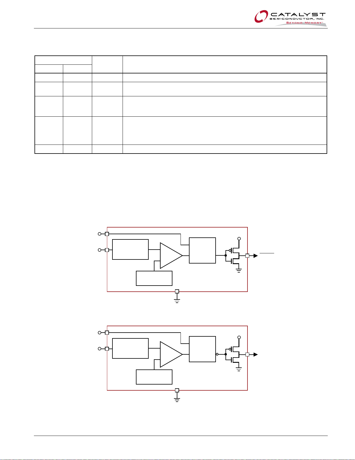
BLOCK DIAGRAM
MR
CC
MR
CC
V
CC
TOLERANCE
BIAS
V
CC
TOLERANCE
BIAS
+
–
VOLTAGE
REFERENCE
+
–
GND
RESET
&
DIGITAL
DELAY
RESET
&
DIGITAL
DELAY
V
CC
CAT811
V
CC
RESET
RESET
VOLTAGE
REFERENCE
CAT812
GND
Doc. No. MD-3005 Rev. S 2 © Catalyst Semiconductor, Inc.
Characteristics subject to change without notice

CAT811, CAT812
ABSOLUTE MAXIMUM RATINGS
(1)
Parameters Ratings Units
Any pin with respect to ground -0.3 to + 6.0 V
Input Current, V
Output Current RESET, RESET
Rate of Raise, V
CC
¯¯¯¯¯¯
CC
Continuous Power Dissipations
20 mA
20 mA
100 V/µs
320 mW
Derate 4mW/ºC above +70ºC (SOT-143)
Storage Temperature -65 to +105 ºC
Operating Ambient Temperature -40 to +85 ºC
Lead Soldering (10 seconds) +300 ºC
ELECTRICAL OPERATING CHARACTERISTICS
VCC = Full range, TA = -40°C to +85°C unless otherwise noted. Typical values at TA = +25°C and VCC = 5V for the
L/M/J versions, V
Parameter Symbol Conditions Min Typ Max Units
VCC Range
Supply Current ICC TA = -40˚C to +85˚C
Reset
Threshold
Voltage
= 3.3V for the T/S versions, VCC = 3V for the R version and VCC = 2.5V for the Z version.
CC
TA = 0°C to +70°C 1.0 5.5
T
= -40°C to +85°C 1.2 5.5
A
VCC < 5.5V, J/L/M 8 20
V
< 3.6V, R/S/T/Z 6 15
CC
L Threshold
M Threshold
J Threshold
T Threshold
V
TH
S Threshold
R Threshold
Z Threshold
TA = +25°C 4.56 4.63 4.70
T
= -40°C to +85°C 4.50 4.75
A
TA = +25°C 4.31 4.38 4.45
T
= -40°C to +85°C 4.25 4.50
A
TA = +25°C 3.93 4.00 4.06
T
= -40°C to +85°C 3.89 4.10
A
TA = +25°C 3.04 3.08 3.11
T
= -40°C to +85°C 3.00 3.15
A
TA = +25°C 2.89 2.93 2.96
T
= -40°C to +85°C 2.85 3.00
A
TA = +25°C 2.59 2.63 2.66
T
= -40°C to +85°C 2.55 2.70
A
TA = +25°C 2.28 2.32 2.35
T
= -40°C to +85°C 2.25 2.38
A
V
µA
V
Notes:
(1) Stresses above those listed under “Absolute Maximum Ratings” may cause permanent damage to the device. These are stress ratings
only, and functional operation of the device at these or any other conditions outside of those listed in the operational sections of this
specification is not implied. Exposure to any absolute maximum rating for extended periods may affect device performance and reliability.
© Catalyst Semiconductor, Inc. 3 Doc. No. MD-3005 Rev. S
Characteristics subject to change without notice
CAT811, CAT812
ELECTRICAL OPERATING CHARACTERISTICS (continued)
VCC = Full range, TA = -40°C to +85°C unless otherwise noted. Typical values at TA = +25°C and VCC = 5V for the
L/M/J versions, V
Parameter Symbol Conditions Min Typ
Reset Threshold
Tempco
VCC to Reset
(2)
Delay
Reset Active
Timeout Period
¯¯¯¯¯¯
RESET
Output
Voltage Low
(Push-pull, active
LOW, CAT811)
¯¯¯¯¯¯
RESET
Output
Voltage High
(Push-pull, active
LOW, CAT811)
RESET Output
Voltage Low
(Push-pull, active
HIGH, CAT812)
RESET Output
Voltage High
(Push-pull active
HIGH, CAT812)
¯¯¯
MR
Minimum
Pulse Width
¯¯¯
MR
Glitch
Immunity
¯¯¯
MR
to RESET
Propagation Delay
¯¯¯
MR
Input
Threshold
= 3.3V for the T/S versions, VCC = 3V for the R version and VCC = 2.5V for the Z version.
CC
(1)
Max Units
30 ppm/˚C
V
T
V
OL
V
OH
V
OL
V
OH
10 µs
t
MR
= VTH to (VTH - 100mV) 20 µs
CC
= -40˚C to +85˚C 140 240 400 ms
A
VCC = V
CAT811R/S/T/Z
VCC = V
CAT811J/L/M
> 1.0V, I
V
CC
VCC = V
CAT811R/S/T/Z
V
= V
CC
CAT811J/L/M
VCC > V
CAT812R/S/T/Z
V
> V
CC
CAT812J/L/M
1.8 V < V
I
SOURCE
, I
TH min
SINK
, I
TH min
SINK
SINK
, I
TH max
TH max
TH max
TH max
CC
, I
, I
, I
V
SOURCE
SOURCE
SINK
SINK
TH min
= 150µA
= 1.2mA
= 3.2mA
0.3
0.4
= 50µA 0.3
= 500µA
= 800µA
= 1.2mA
= 3.2mA
,
0.8V
V
0.8V
CC
- 1.5
CC
0.3
0.4
V
CC
Note 3 100 ns
Note 2 0.5 µs
t
MD
V
VCC > V
IH
V
0.8 V
IL
V
VCC > V
IH
, CAT811/812L/M/J 2.3V
TH (MAX)
, CAT811/812R/S/T/Z 0.7VCC
IH (MAX)
V
V
V
V
0.25V
IL
¯¯¯
MR
Pull-up
Resistance
Notes:
(1) Production testing done at T
¯¯¯¯¯¯
(2) RESET
(3) Glitches of 100ns or less typically will not generate a reset pulse
Doc. No. MD-3005 Rev. S 4 © Catalyst Semiconductor, Inc.
output for the CAT811; RESET output for the CAT812
10 20 30 k
= +25˚C; limits over temperature guaranteed by design only.
A
Characteristics subject to change without notice
CC

CAT811, CAT812
Y
R
A
T
E
U
)
0
TYPICAL OPERATING CHARACTERISTICS
VCC = Full range, TA = -40°C to +85°C unless otherwise noted. Typical values at TA = +25°C and VCC = 5V for the
L/M/J versions, V
= 3.3V for the T/S versions, VCC = 3V for the R version and VCC = 2.5V for the Z version.
CC
POWER-UP RESET TIMEOU
VS. TEMPERATUR E
260
T (ms
240
TTIMEO
220
200
180
POWER-UP RES
160
-50 0 50 100 150
VCC=5V
VCC=2.5V
TEMPERATURE (°C)
SUPPLY CURRENT (µA)
SUPPL
CURRENT VS. TEMPE
(NO LOAD, CAT8xxR/S/T/Z)
12
10
8
6
4
2
0
-50 0 50 100 150
TEMPERATURE (°C)
VCC=5.5V
TURE
VCC=3.6V
POWER-DOWN RESET DELAY VS. TEMPERATURE
14
12
10
8
6
4
2
0
POWER-DOWN RESET DELAY (s)
-50 0 50 100 150
(CAT8xxR/S/T/Z)
TEMPERATURE (°C)
1.0002
0.9998
0.9996
0.9994
0.9992
NORMALIZED THRESHOLD
0.9988
0.999
NORMALIZED RESET THRESHOLD
VS. TEMPERATURE
1
0 20 40 60 80 100 12
TEMPERATURE (°C)
© Catalyst Semiconductor, Inc. 5 Doc. No. MD-3005 Rev. S
Characteristics subject to change without notice

CAT811, CAT812
V
DETAILED DESCRIPTION
RESET TIMING
The reset signal is asserted LOW for the CAT811 and
HIGH for the CAT812 when the power supply voltage
falls below the threshold trip voltage and remains
asserted for at least 140ms after the power supply
voltage has risen above the threshold.
Power
oltage
5V
0V
5V
0V
Supply
RESET
Threshold
Volta ge
Reset Timeout Period
140ms
minimum
CAT811
RESET
5V
0V
Figure 1. Reset Timing Diagram
VCC TRANSIENT RESPONSE
The CAT811/812 protect µPs against brownout
failure. Short duration transients of 4µs or less and
100mV amplitude typically do not cause a false
RESET.
Figure 2 shows the maximum pulse duration of
negative-going V
transients that do not cause a
CC
reset condition.
30
25
20
15
10
CAT812
As the amplitude of the transient goes further below
the threshold (increasing V
pulse duration decreases. In this test, the V
- VCC), the maximum
TH
starts
CC
from an initial voltage of 0.5V above the threshold and
drops below it by the amplitude of the overdrive
voltage (V
- VCC).
TH
T
= 25°C
AMB
CAT8xxZ
5
TRANSIENT DURA TION (s)
CAT8xxM
0
1 10 100 1000
RESET OVERD R IVE VTH - VCC (mV)
Figure 2. Maximum Transient Duration without Causing a
Reset Pulse vs. Reset Comparator Overdrive
Doc. No. MD-3005 Rev. S 6 © Catalyst Semiconductor, Inc.
Characteristics subject to change without notice

CAT811, CAT812
VALID RESET WITH VCC UNDER 1.0V
To ensure that the CAT811 RESET
state when V
resistor between RESET
is under 1.0V, a 100k pull-down
CC
¯¯¯¯¯¯
¯¯¯¯¯¯
pin is in a known
pin and GND is
recommended; the value is not critical. For the
CAT812, a pull-up resistor from RESET pin to V
CC
is
needed.
Power
Supply
V
CC
CAT811
MR RESET
Figure 3. RESET
¯¯¯¯¯¯
GND
Valid with V
CC
100k
under 1.0V
Power
Supply
V
CC
CAT812
MR RESET
GND
Figure 4. RESET Valid with V
100k
under 1.1V
CC
BI-DIRECTIONAL RESET PIN INTERFACING
The CAT811/812 can interface with µP/µC bidirectional reset pins by connecting a 4.7k resistor in
series with the CAT811/812 reset output and the
µP/µC bi-directional reset pin.
Power
Supply
CAT811
4.7k
MR
RESET
GND
Bi-directional I/O Pin
Figure 5. Bi-directional Reset Pin Interfacing
RESET
INPUT
BUF
V
µP
CAT811
GND
CC
Buffered
RESET
(for example: 68HC11)
© Catalyst Semiconductor, Inc. 7 Doc. No. MD-3005 Rev. S
Characteristics subject to change without notice

CAT811, CAT812
OTHER SUPERVISORY PRODUCTS
Function CAT1161/3 CAT1162 CAT809 CAT810 CAT811 CAT812
With 16k Bit Serial EEPROM
Memory
Watchdog Timer
Manual Reset Input
Active Low Reset
Active High Reset
Dual Polarity Reset Outputs
Package
8-pin DIP
and SOIC
8-pin DIP
and SOIC
3-pin SOT-23
and SC70
3-pin SOT-23
and SC70
4-pin
SOT-143
4-pin
SOT-143
Doc. No. MD-3005 Rev. S 8 © Catalyst Semiconductor, Inc.
Characteristics subject to change without notice

CAT811, CAT812
PACKAGE OUTLINE DRAWING
SOT-143 4-Lead (TB)
(1)
D
e1
TOP VIEW
SYMBOL MIN NOM MAX
A 0.80 1.22
A1 0.05 0.15
e
A2 0.75 0.90 1.07
b 0.30 0.50
b2 0.76 0.89
c 0.08 0.20
D 2.80 2.90 3.04
E1 E
E 2.10 2.64
E1 1.20 1.30 1.40
e 1.92 BSC
e1 0.20 BSC
b
L 0.40 0.50 0.60
L1 0.54 REF
L2 0.25
0° 8°
A2
b1
SIDE VIEW END VIEW
A1
For current Tape and Reel inform ation, do wnload the PDF fil e from:
http://www.catsemi.com/documents/tapeandreel.pdf.
Notes:
(1) All dimensions are in millimeters. Angles in degrees.
(2) Complies with JEDEC satndard TO-253.
L2
A
L
L1
c
© Catalyst Semiconductor, Inc. 9 Doc. No. MD-3005 Rev. S
Characteristics subject to change without notice

CAT811, CAT812
EXAMPLE OF ORDERING INFORMATION
Prefix
Device # Suffix
(1)
CAT 811 S TB I -G T10
Company ID
Product Number
811: Push-Pull/Active Low Output
812: Push-Pull/Active High Output
Trip Level
L: 4.63V
M: 4.38V
J: 4.00V
T: 3.08V
S: 2.93V
R: 2.63V
Z: 2.32V
Package
TB: SOT-143
Temperature Range
I = Industrial (-40ºC to 85ºC)
Lead Finish
Blank: Matte-Tin
G: NiPdAu
T: Tape & Reel
3: 3,000/Reel
10: 10,000/Reel
Tape & Reel
For Product Top Mark Codes, click here:
http://www.catsemi.com/techsupport/producttopmark.asp
Notes:
(1) All packages are RoHS-compliant (Lead-free, Halogen-free).
(2) The standard lead finish is NiPdAu. Contact factory for other package availability.
(3) This device used in the above example is a CAT811STBI-GT10 (SOT-143 4-Lead, Push-Pull/Active Low Output, trip level of 2.85V to
3.00V, NiPdAu, Tape & Reel, 10,000/Reel)
(4) For additional package and temperature options, please contact your nearest Catalyst Semiconductor Sales office.
Doc. No. MD-3005 Rev. S 10 © Catalyst Semiconductor, Inc.
Characteristics subject to change without notice

REVISION HISTORY
Date Rev. Reason
10/22/2003 L Updated Ordering Information
12/22/2003 M
03/22/2004 N General data sheet updates
03/25/2004 O Updated Electrical Characteristics (Reset Active Timeout Period Max)
03/25/2004 P Corrected Pin Configure diagram
09/28/2004 Q Minor changes
12/28/2005 R Updated Features Updated Ordering Information Updated Top Marking
04/18/2008 S
Updated Features Replaced power-up reset timeout vs. temperature graph with updated
one Replaced V
Transient Response graph with updated one
CC
Add “MD-“ to document number
Add Block Diagrams
Updated Package Outline Drawing
Update Example of Ordering Information
Copyrights, Trademarks and Patents
© Catalyst Semiconductor, Inc.
Trademarks and registered trademarks of Catalyst Semiconductor include each of the following:
Adaptive Analog™, Beyond Memory™, DPP™, EZDim™, LDD™, MiniPot™, Quad-Mode™ and Quantum Charge Programmable™
Catalyst Semiconductor has been issued U.S. and foreign patents and has patent applications pending that protect its product s.
CATALYST SEMICONDUCTOR MAKES NO WARRANTY, REPRESENTATION OR GUARANTEE, EXPRESS OR IMPLIED, REGARDING THE SUITABILITY OF ITS
PRODUCTS FOR ANY PARTICULAR PURPOSE, NOR THAT THE USE OF ITS PRODUCTS WILL NOT INFRINGE ITS INTELLECTUAL PROPERTY RIGHTS OR THE
RIGHTS OF THIRD PARTIES WITH RESPECT TO ANY PARTICULAR USE OR APPLICATION AND SPECIFICALLY DISCLAIMS ANY AND ALL LIABILITY ARISING
OUT OF ANY SUCH USE OR APPLICATION, INCLUDING BUT NOT LIMITED TO, CONSEQUENTIAL OR INCIDENTAL DAMAGES.
Catalyst Semiconductor products are not designed, intended, or authorized for use as components in systems intended for surgical implant into the body, or other
applications intended to support or sustain life, or for any other application in which the failure of the Catalyst Semiconductor product could create a situation where personal
injury or death may occur.
Catalyst Semiconductor reserves the right to make changes to or discontinue any product or service described herein without notice. Products with data sheets labeled
"Advance Information" or "Preliminary" and other products described herein may not be in production or offered for sale.
Catalyst Semiconductor advises customers to obtain the current version of the relevant product information before placing orders. Circuit diagrams illustrate typical
semiconductor applications and may not be complete.
Catalyst Semiconductor, Inc.
Corporate Headquarters
2975 Stender Way
Santa Clara, CA 95054
Phone: 408.542.1000 Document No: MD-3005
Fax: 408.542.1200 Revision: S
www.catsemi.com Issue date: 04/18/08
 Loading...