

Page 1

(with price)
INDEX
LCD VIDEO MONITOR
VM-570B
JUNE 1994
Page
Specifications.............................................................................................1
Block Diagram ...........................................................................................2
Power Supply.............................................................................................3
Adjustment
Linear PCB..........................................................................................4
A/D PCB..............................................................................................6
Printed Circuit Boards................................................................................7
Wiring Diagram........................................................................................10
Electrical Parts List ..................................................................................11
Mechanical Parts List...............................................................................16
Exploded View / Disassembly..................................................................17
Waveforms...............................................................................................18
Schematic Diagrams................................................................................19
R
Page 2
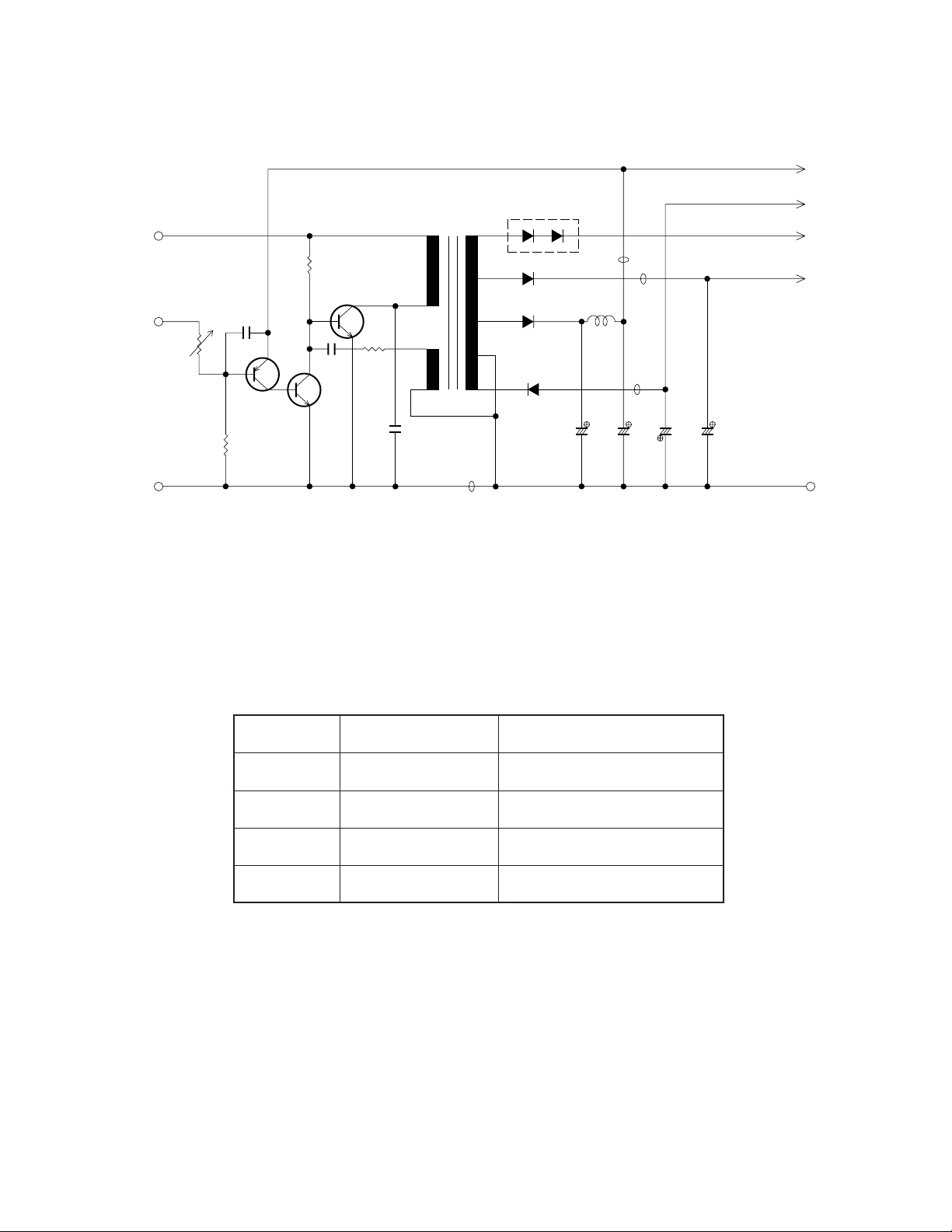
POWER SUPPLY
VCC2
VEE1
VCC7
VCC6
GND
DC 6V
from IC400
Vref
GND
C151
Q100
R101
R103
C152
Q101
Q102
R104
C153
T100
LC12U-21
2
1
9
8
D115
3
4
D116
5
D117
6
7
D118
L101
C115
C116
C117
C118
Fig. 3
The power supply consists of DC-DC converter, and causes the voltages to be output as shown in Table - 2.
Name Voltage Function
VCC2 4.0 ± 0.02V Main voltage
VCC6 48.0 ~ 72.0V Tuning voltage
VCC7 28.0 ~ 40.0V Display voltage
VEE1 -8.4 ~ -5.6V Display voltage
Table - 2
— 3 —
Page 3
ADJUSTMENT
Linear PCB
1) Items to Be Adjusted:
Item Measuring Instrument
VCC2 voltage setting Voltmeter
Contrast adjustment TV signal generator, Pattern generator, Oscilloscope
AGC adjustment TV signal generator, Pattern generator, IF levelmeter
2) Adjustment and Test Point Locations:
TOP VIEW
TP1
VR100
— 4 —
Page 4
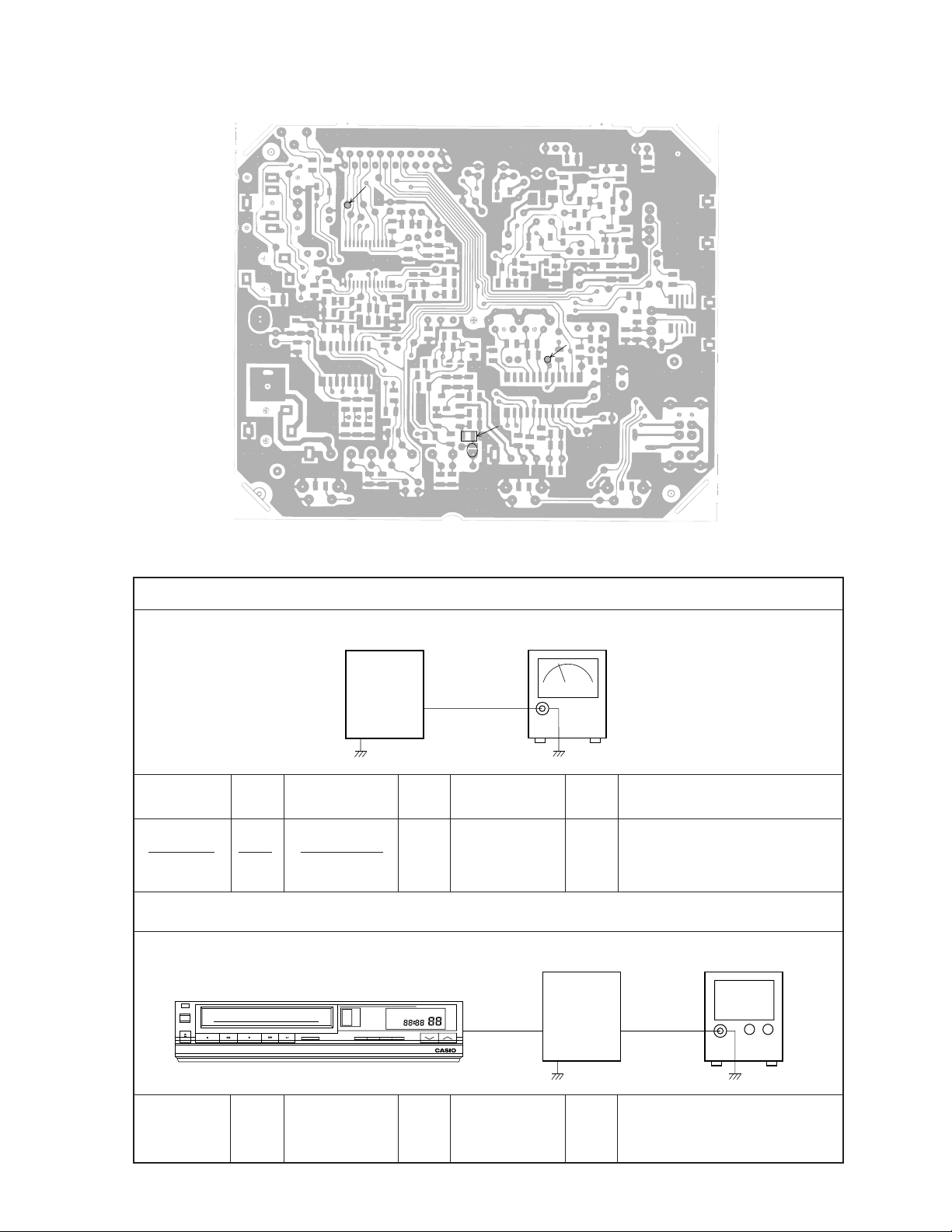
TP5
BOTTOM VIEW
TP3
R200
TP2
Pad IF
3) Equipment Connection / Procedure
Vcc2 Voltage Setting
Set
Voltmeter
Output
TP1
Input Input Input Output Output
Connection Point Signal Connection Point
Adjust Adjust for
VR100 TP1
Voltmeter
Adjust for 4.00 ± 0.02V
reading on voltmeter.
* Open soldering pad IF.
VHS
HQ
AV
Jack
Color bar
Contrast Adjustment
PLAY
Input Output
AV-C1
cord
OscilloscopeVCR VR300 TP5
— 5 —
Set Oscilloscope
TP5
Adjust step form wave to read
0.8 ± 0.05 Vp-p.
Page 5
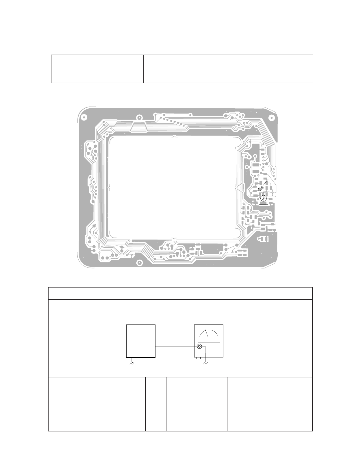
A/D PCB
1) Item to Be Adjusted:
Item Measuring Instrument
Clock adjustment Voltmeter
2) Adjustment and Test Point Locations:
TOP VIEW
TP6
3) Equipment Connection / Procedure
Set
VR700
Clock Adjustment
Voltmeter
Output
TP6
Input Input Input Output Output
Connection Point Signal Connection Point
Adjust Adjust for
VR700
Voltmeter
— 6 —
TP6
Adjust for 2.00 ± 0.05V
reading on voltmeter.
Page 6

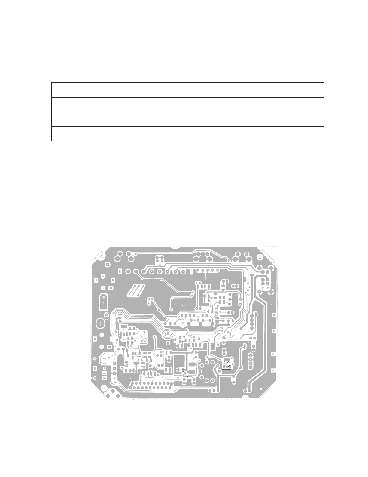
PRINTED CIRCUIT BOARDS
Linear PCB (Top View)
C410
SW100
R321
VR301
JK600
JK250
C317
C313
R325
Q300
R329
VR
300
R308
Linear PCB (Bottom View)
R323 R322
R312
R310
R320
C356
R603
C355
C450
C357 @
IC400
R326
R327
R328
R307
R302
IC300
R314
R313
H300
C310
C312
CN700
C351
C352
R318
R317
C311
R340
R305
R304
R315
R120
R306
C350
R301
C315
C116
C119
R303
C358
R316
C359
D110
R435
C115
C117
D118
R114
L101
T100
R104
D117
D116
CN600
C190
R103
D115
C610
C118
VR
100
CN100
C110
Q102
C153
C152
Q101
Q100
R100
C151
R606 R605
R101
C653
R602
C652
C611
C612
FU100
C160
R601
VR600
VR800
R600
IC600
— 7 —
Page 7

A/D PCB (Top View)
C762
D710
C782
D730
R720
C700
C761
C781
L701
C780
VR700
R709
R721
C783
D700
C811
C813
C812
BL PCB (Top View)
C810
C815
CN300
Q900
L900
R900
Q901
C952
C850
C770
R800
T900
C710
D711
R722
R804
C953
DC PCB (Top View)
JK100
D150
— 8 —
Page 8

A/D PCB (Bottom View)
R716
R717
C776
C763
C777
IC700
C775
R704
R702 R701
R708
R707
R715
R703
R710
L700
R712
(C.D)
R711
(A.B)
R700
C771
R820
R806
C855
C772
D800
R815
R801
C860
R818
R819 R816
Q802 D810 D811
Q801
R807
R802
R803
Q806
Q805
C856
C861
R817
R808
Q800
— 9 —
Page 9

A/D PCB
WIRING DIAGRAM
Linear PCB
1
22
122
— 10 —
Page 10

EXPLODED VIEW / DISASSEMBLY
1
2
34
4
5-1
2-2
2-2
2-1
2-2
2-4
2-3
2-5
37
29
12
5
13
14
7
31
9
32
33
32
10
8
30
6
35
21
22
36
20
19
26
22
16-1
25
23-3
23-4
15
16-2
16
17
23-1
23-5
23
28
11 @@
— 17 —
Page 11

WAVEFORMS
1.0V
1 IC300 Pin 1
4 IC300 Pin 4
64µsec
64µsec
600mV
2.4V
2.5V
0.22µsec
2 IC300 Pin 23
5 IC300 Pin 5
64µsec
2.6V
2.3V
2.1V
64µsec
3 IC300 Pin 10, 11, 12
14V
3.9µsec
6 Q102 Collector
2.2V
7 Q102 Base
0 Q800 Base
4.0µsec
132µsec
420mV
8 IC700 Pin 17
A IC700 Pin 12
152nsec 547nsec
9 IC700 Pin 14
2.5V
63.5µsec
— 18 —
Page 12

Linear PCB
SCHEMATIC DIAGRAMS
2
3
1
TP5
7
6
TP1
5
4
— 19 —
Page 13

A/D PCB
10
8
11
TP6
9
— 20 —
Page 14

BL PCB
VCC1-1
To Linear PCB
GND
SP
1
EYP-1BF102L
C952
ECQ-V1H184JZ
Q900
2SD965-R
Q901
2SD965-R
L900
RCH-875-101K
T900
NT-01
5
4
3
2
112
10
C953
DE0905
SL181J2K
EYP-1BF102L
LAMP
3
2
SP
— 21 —
 Loading...