

Page 1
SERVICE MANUAL
INDEX
VAN MECHELEN
www.vanmechelen.be
(without price)
UP-360
JAN. 2004
Page 2

CONTENTS
UP-360 PAGE
1. SPECIFICATIONS
1-1. PRINTING SPECIFICATION .............................................................................1
1-2. PAPER SPECIFICATION..................................................................................1
1-3. INTERFACE SPECIFICATION..........................................................................2
2. DISASSEMBLY............................................................................................ 4
3. CIRCUITRY
3-1. SYSTEM BLOCK DIAGRAM ............................................................................8
3-2. POWER SUPPLY CIRCUIT ..............................................................................9
3-3. POWER SUPPLY SPECIFICATION ...............................................................11
3-4. HD64F7045F MICROCOMPUTER..................................................................12
3-5. RESET CIRCUIT .............................................................................................20
3-6. DRAWER CIRCUIT .........................................................................................20
3-7. BUZZER CIRCUIT...........................................................................................21
3-8. FLASH MEMORY CIRCUIT ............................................................................21
3-9. EXTERNAL MEMORY CIRCUIT.....................................................................22
3-10. CHARACTER GENERATOR CIRCUIT...........................................................23
3-11. PRINTER CIRCUIT..........................................................................................23
3-12. SERIAL INTERFACE CIRCUIT.......................................................................25
4. MAINTERNANCE & TROUBLESHOOTING
4-1. INSTALLING OR REPLACING PAPER ROLL...............................................26
4-2. ADJUSTING THE PAPER NEAR END SENSOR (TH200s ONLY) ...............26
4-3. PAPER JAM....................................................................................................27
4-4. TROUBLESHOOTING ....................................................................................27
4-5. SELF TEST......................................................................................................29
5. SETTING & CHECKING THE DIP SWITCHES ........................................ 30
6. CIRCUIT DIAGRAMS................................................................................. 31
7. PARTS LIST............................................................................................... 34
Page 3

1. SPECIFICATIONS
1-1. PRINTING SPECIFICATION
Model NO. of Printer Mechanism: LTPF347A-C576 *1
Printing Method: Direct Line Thermal
Dot pitch: 8 dot / mm
Printing Speed: 210 mm per second (Max.)
Printing width: 72mm / 576 dots
Character structure: 8 x 16 (font B) 12 x 24 (font A)
Printing Columns: 69 columns / line 46 columns / line
Character Size: 1.00 x 2.00 1.50 x 3.00
Feed Speed: 220 mm per second
Interface: RS232C (serial)
Input buffer: 8k bytes
Command: ESC / POS compliant
Paper Width & Diameter: 80 mm (W) x 80 mm Dia. Max.
Thermal head life: 100 Million Pulses / 100 km or more
Cutting method: *2 ACUF324A
Partial cut(one point left uncut) *2
Auto cutter life: 500,000 cuts
Operating time of auto cutter: 600 msec max/cycle
Operating temperature: 0 °C ~ 40 °C
Storage temperature: -20 °C ~ 50 °C
Humidity: 80 %
Dimension: 145 mm (W) x 193.2 mm (L) x 120.1 mm (H)
Transfer speed: Max 38.4 kBps
Supply voltage in standby: 24V DC / 100mA
Mean voltage: Approx. 1.3 A *3
Power Consumption: Approx. 4 W *3
Weight: 1.1kg
*1 Manufactured by SIIP&S Inc. (Former name: Seiko Instruments Inc.)
*2 CAUTION: Paper must be fed 3 mm after cutting to prevent paper jam.
*3 These values vary according to environmental temperature when printed font A(12 x 24) with a rolling pattern.
1-2. PAPER SPECIFICATION
Paper Width: 79.5 ± 0.5mm (3.13 ± 0.02”)
Paper roll size: Roll diameter: Maximum 80 mm (3.15”)
Take-up paper roll width: 80 + 0.5/-1.0mm (3.15 + 0.02/-0.04”)
Specified paper: Specified thermal roll paper: NTP080-80
[Original paper:TF50KS-E2C Nippon Paper Industries Co., Ltd.]
Packaged roll paper:
[Original paper:PD160R-N (Oji Paper Mfg. Co., Ltd.)]
In Japan: Nakagawa Manufacturing Co., Ltd.
In U.S.A: Nakagawa Mfg. (U.S.A.) Inc.
In Europe: Nakagawa Mfg. (Europe) GmbH
In Southeast Asia: N.A.K. Mfg. (Malaysia) SDN BHD
*The following paper can be used instead of the paper above:
Original paper: HP220AB1 (Mitsubishi Paper Mills Ltd.)
Paper roll spool diameter: Inside 12 mm (0.47”)
Outside 18 mm (0.71”)
NOTE:The end of the paper roll must be free to come off the spool when finished. It must not be adhesively
attached or attached in another semi-permanent manner.
— 1 —
Page 4
1-3. INTERFACE SPECIFICATION
1-3-1. RS-232 SERIAL INTERFACE SPECIFICATION
Data transmission: Serial. EIA RS232C compliant
Synchronization: Asynchronous
Handshaking: DTR/DSR or XON/XOFF control (*)
Signal levels: MARK = -3 to -15V: Logic “1”/OFF
SPACE = +3 to +15V: Logic “0”/ON
Baud rate: 9600, 19200, 38400bps (*)
Data word length: 8 bits
Parity Settings: None, even, odd (*)
Stop bits: 1 or more
Connector (printer side): Female DSUB-25 pin connector
Notes: *The data word length, baud length, and parity depend on the DIP switch settings. (Refer to
5.SETTING & CHECKING THE DIP SWITCHES.)
1-3-2. SERIAL INTERFACE CONNECTION EXAMPLE
HOST SIDE PRINTER SIDE
(DTE ex.8251) (Pin No.)
TxD RxD (3)
RxD TxD (2)
DTR DSR (6)
DSR DTR (20)
RTS
CTS
GND GND (7)
FG FG (1)
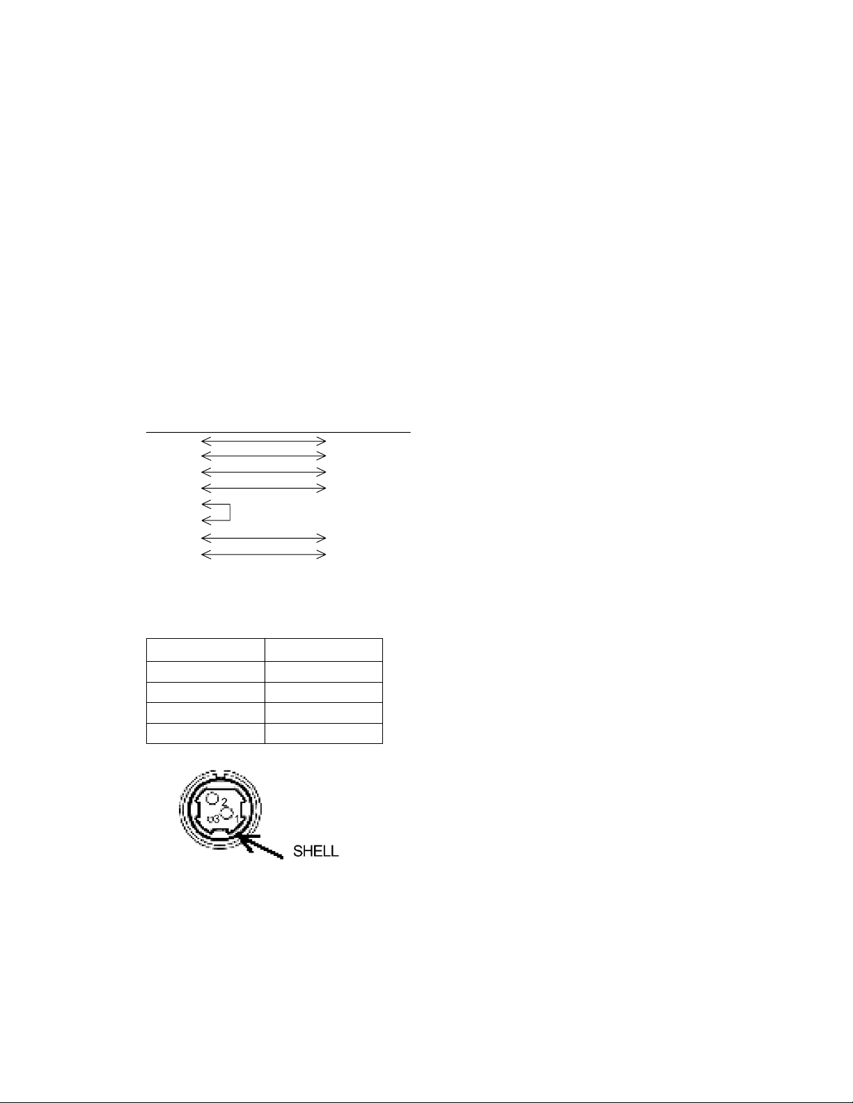
1-3-3. POWER SUPPLY CONNECTOR
The connector is connected the printer to an external power source.
CONNECTOR MODEL:
PIN SIGNAL
1 +24V
2 GND
3NC
SHELL F. G
Printer side: Hosiden TCS7960-532010 or equivalent
User side: Hosiden TCP8927-631100 or equivalent
Hosiden TCP8927-531100 or equivalent
— 2 —
Page 5
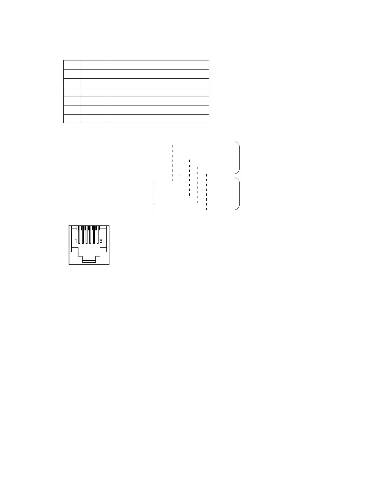
1-3-4. DRAWER KICK-OUT CONNECTOR
The pulse specified by ESC p or DLE DC4 is output to this connector. The HOST can confirm the status
of the input signal by using the DLE EOT, GS a, or GS r commands.
PIN I/O DESCIPTION
1 - Frame ground
2 Output Drawer kick-out drive signal 1
3 Input Drawer open/close signal
4 Output +24 V
5 Output Drawer kick-out signal 2 *
6 - Signal ground
* Two drawers can be used with a Y-cable that meets the following specifications.
Pin 1: Frame ground ............................................................ Pin1
Pin 2: Drawer kick-out drive signal 1 ................................... Pin2
Pin 3: Drawer open/close signal .......................................... Pin3 Connector of Drawer No.1
Pin 4: +24V .......................................................................... Pin4
Pin 5: Drawer kick-out signal 2 .................... ......... Pin6
Pin 6: Signal ground Pin6 ............. ............................. Pin1
........................ Pin2
................... Pin3 Connector of Drawer No.2
.............. Pin4
....................................... Pin6
CONNECTIOR MODEL:
Printer side: MOLEX52065-6615 or equivalent
Used side: 6-position 6-contact (RJ12 telephone jack)
— 3 —
Page 6
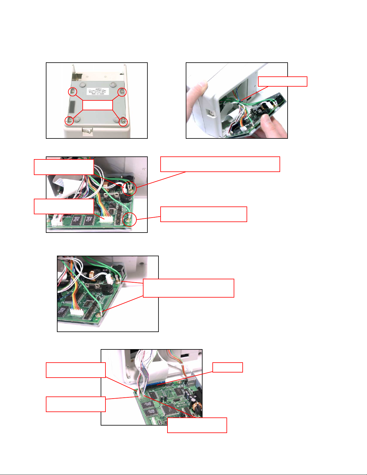
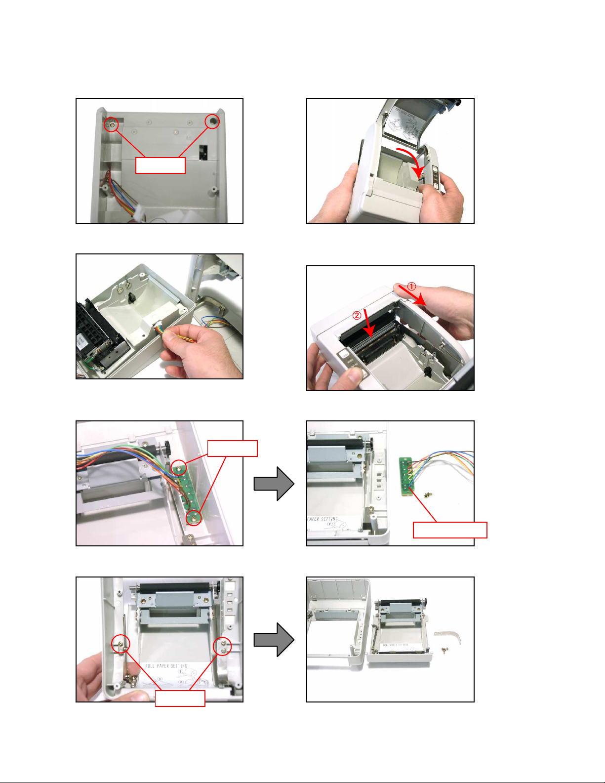
2. DISASSEMBLY
1. Remove the four screws at the bottom of the printer unit.
2. Remove the cable tie.
Screws
3. Remove the two connectors and two screws (CN5, CN6).
Cable tie
CN6
(To Power Switch)
CN5
(To Contorl Panel)
(Earth wires for the printer and the auto cutter)
(An earth wire for the NE sensor)
Precaution when assembling:
Bend the rug terminal in L shape and put it inside the PCB.
NG example
The rug terminal faces outward.
Screw
Screw
4.Remove the three connectors (CN, CN2, CN3) and the FPC (J1), and then remove the main PCB.
CN3
(To NE Sensor)
CN2
(To Auto Cutter)
CN
(To Printer Motor)
— 4 —
FFC (J1)
Page 7
5. Remove the two screws.
6. Remove the upper cover while the printer cover is open.
Screws
Precaution when assembling:
Let the connector through the hole.
7. Remove the two screws and then the control panel.
Screws
Precaution when assembling:
Slide the lever of the cover to “close” and then fit the
upper cover into the printer.
8. Remove the three screws and then the printer cover.
Screws
— 5 —
Control Panel
Page 8
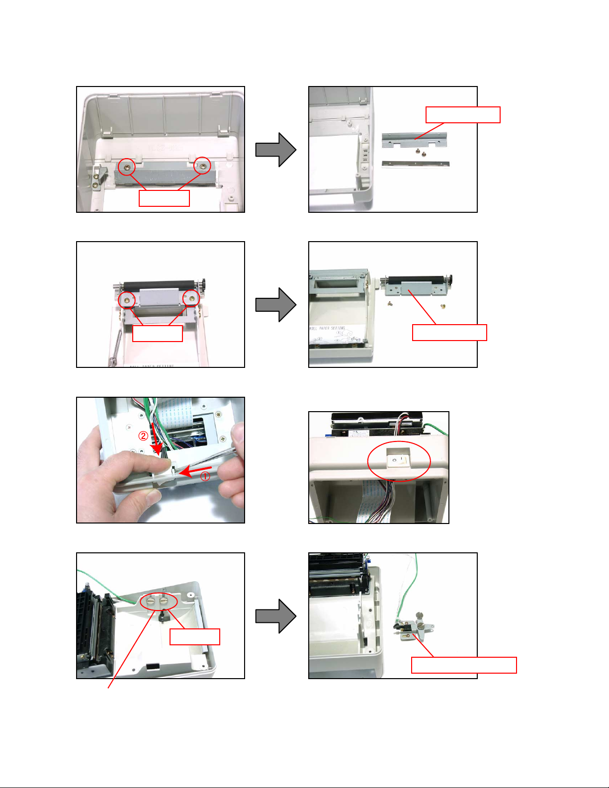
9. Remove the two screws and then the paper guide and the cutter.
Screws
10. Remove the two screws and then the platen unit.
Paper guide
Screws
11. Remove the power switch.
Direction of the power switch when assembling
12. Loosen the two screws and then remove the end sensor unit.
Platen unit
Loosen
Precaution when assembling
Fix the end sensor unit at the lowest of the groove.
— 6 —
End sensor unit
Page 9
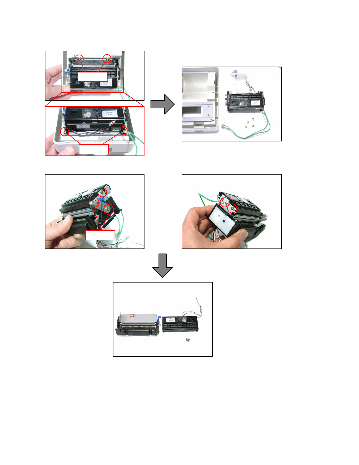
13. Remove the four screws and then the printer unit.
Screws
Screws
14. Remove the five screws and then the printer.
Screws
— 7 —
Page 10
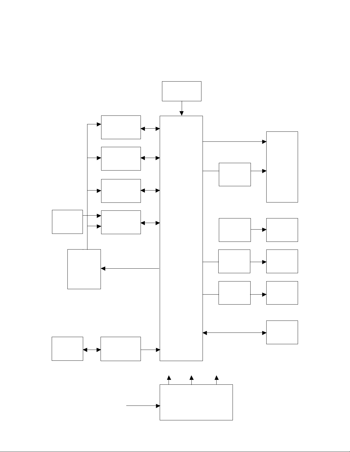
3. CIRCUITRY
3-1. SYATEM BLOCK DIAGRAM
The terminal that wses 16 bits single chip microcomputer. The CPU has 256K Flash ROM and 4K bytes of internal
RAM.
External memory are 128K bytes SRAM 2 pcs, Flash memory (NV bit-image) and Character generator.
Clock
6.754MHz
SRAM
128K x 2 bytes
Printer
Head
FLASH ROM
512K bytes
Character
Generator
Motor
Drive
L6219
Motor
DIP SW
74LV139
Serial
Interface
RS232C
Decode
74LV541
HIN232CB
CPU
HD64F7045
VP VCC RESET
Driver
MB3853
Driver
Driver
TD62308
Auto
Cutter
LED
Panel SW
Drawer
Unit
Near
End sens.
+24V
Power Supply
— 8 —
Page 11
3-2. POWER SUPPLY CIRCUIT
The power supply source is a DC 24V.
+24V(VP)
Power supply voltage.
+24V(HVP)
The printer motor and head voltages are the +24V same as source voltage.
+5V (VCC)
The circuit generating the +5V uses the 24V.It apply the switting-circut of a M5291 , 2SB1455 and Coil (SFT8-40S).
POWER SUPPLY CIRCUIT continued
VP
VP
CN6
POWER
SW
1
2
B2P-SHF-1AA
CN7
1
2
3
TCS796053-2010
R185
0
R182
F2
125V/3A
FB3
MPZ3216S500A
FB2
MPZ3216S500A
C81
1M
1000pF
— 9 —
Page 12
HVP for VP
HVPSW
VCC
R147
10K
R141
3.3K
Q3
2SA1037
R143
10K
R148
3.3K
R145
R140
Q2
2SC2412
680 1%
10K
VP
10K
R137
Q1
2SJ553S
R144
56.2K 1%
3
1
DA1
1SS319
4
2
C55
0.1uF
R146
10K 1%
HVP
SHVP
HVCCSW#
POWER SUPPLY CIRCUIT continued
VCC for VP
VP
R181
+
27 1W DIP
C79
100uF/50V
U21
8
Qo
7
Ipek
6
Vin
5
Vref
M5291F
R184
1.1K 1%
R183
3.6K 1%
C56
100pF
SC
SE
Co
GND
SHR
R179
100
1
2
3
4
R180
300 1/2W
C80
330pF
Q7
2SB1455
D7
EC20QS6
+
L5
SF-T8-40S
VCC
C82
1000uF/10V
— 10 —
Page 13

3-3. POWER SUPPLY SPECIFICATION
Input-Power Consumption
Input: DC24V ±10%
Standing
by : Maximum 10 watts
Printing : Maximum 48 watts
Output-Rated Voltage
Voltage : 24±2.0V Standing by
VP to GND Ripple : Less than 0.3V p-p Printing
Stability : Line regulation-less than 0.5V Viac –10% to +10%
Temp. regulation-less than 0.5V Temp. 0°C to 40°C
Voltage : 5.0V±0.25V Standing by
VCC to GND Ripple : Less than 0.2V p-p Printing
Stability : Line regulation-less than 0.2V Viac –10% to +10%
Temp. regulation-less than 0.2V Temp. 0°C to 40°C
— 11 —
Page 14

3-4. HD64F7045F MICROCOMPUTER
Description
The M3612SAFP is a single-chip microcomputer designed with CMOS silicon gate technology.
It is housed in a 100-pin QFP.
In addition to its simple instruction sets, the ROM, RAM and I/O addresses are placed on the
same memory map to enable easy programming.
PIN Configuration (Top view)
10
11
12
13
14
15
16
17
18
19
20
21
22
23
24
25
26
27
28
29
30
31
32
33
34
35
36
1
2
3
4
5
6
7
8
9
U5
PA23
PE14
PA22
PA21
PE15
VSS
PC0/A0
PC1/A1
PC2/A2
PC3/A3
PC4/A4
VCC
PC5/A5
VSS
PC6/A6
PC7/A7
PC8/A8
PC9/A9
PC10/A10
PC11/A11
PC12/A12
PC13/A13
PC14/A14
PC15/A15
PB0/A16
VCC
PB1/A17
VSS
PA20
PA19
PB2
PB3
PA18
PB4
VSS
PB5
144
143
PE13
142
PE12
141
PE11
140
VSS
139
PE10
138
PE9
137
PE8
135
136
PE7
PA5/SCK1
134
VCC
PA4/TXD1
131
133
132
PA3/RXD1
PA2/SCK0
128
129
130
VSS
PA1/TXD0
PA0/RXD0
127
AVref
AVCC
126
125
PF7/AN7
123
124
AVSS
PF6/AN6
PF5/AN5
122
121
PF4/AN4
120
119
PF3/AN3
PF2/AN2
PF1/AN1
118
117
PF0/AN0
116
VSS
PE6
115
PE5
114
PE4
113
PE3
112
111
VCC
110
109
PE2
PE1
PA17/WAIT
PE0
PA15/CK
PLLVss
PLLCAP
PLLVcc
PA16/AH
EXTAL
RES
MD0
MD1
VCC
NMI
MD2
MD3
XTAL
VSS
VSS
VCC
D10
VSS
D11
VCC
D12
D13
D14
D15
108
107
106
105
104
103
102
101
100
99
98
97
96
95
94
93
92
D0
91
D1
90
D2
89
D3
88
D4
87
86
D5
85
84
D6
83
D7
82
D8
81
D9
80
79
78
77
76
75
74
73
HD64F7045F
A1938A2039VCC40A2141VSS42PA1443WDTOVF
A18
37
44
PD3145PD3046WRH
47
48
WRL
49
CS1
50
CS0
PA951PA8
CS3
52
53
54
— 12 —
VSS
CS2
PD2956PD2857PD2758PD2659PD25
55
VSS
VCC
PD24
PD2364PD2265PD2166PD2067PD1968PD1869PD17
60
61
62
63
VSS
PD16
70
71
72
Page 15

Function of HD64F7045
SH7040 Product Overview [HD6437040], [HD6417040]
SH7041 Product Overview [HD6437041], [HD6417041]
SH7042 Product Overview [HD6437042], [HD6477042]
SH7043 Product Overview [HD6437043], [HD6477043]
SH7044 Product Overview [HD64F7044], [HD6437044]
SH7045 Product Overview [HD64F7045], [HD6437045]
CPU:
Original Renesas architecture
32-bit internal data bus
General-register machine
• Sixteen 32-bit general registers
• Three 32-bit control registers
• Four 32-bit system registers
RISC-type instruction set
• Instruction length: 16-bit fixed length for improved code efficiency
• Load-store architecture (basic operations are executed between registers)
• Delayed branch instructions reduce pipeline disruption during branch
• Instruction set based on C language
Instruction execution time: one instruction/cycle (35 ns/instruction at 28.7-MHz operation)
Address space: Architecture supports 4 G bytes
On-chip multiplier: multiplication operations (32 bits x 32 bits 64 bits) and multiplication/accumulation operations
(32 bits x 32 bits + 64 bits 64 bits) executed in two to four cycles
Five-stage pipeline
Cache Memory:
1-kbyte instruction cache
Caching of instruction codes and PC relative read data
4-byte line length (1 longword: 2 instruction lengths)
256 entry cache tags
Direct map method
On-chip ROM/RAM, and on-chip I/O areas not objects of cache
Used in common with on-chip RAM; 2 k bytes of on-chip RAM used as address array/data array
when cache is enabled
Interrupt Controller (INTC):
Nine external interrupt pins (NMI, IRQ0-IRQ7)
Forty-three internal interrupt sources (forty-four for A mask)
Sixteen programmable priority levels
User Break Controller (UBC):
Generates an interrupt when the CPU or DMAC generates a bus cycle with specified conditions
Simplifies configuration of an on-chip debugger
— 13 —
Page 16

Bus State Controller (BSC):
Supports external extended memory access
• 16-bit (QFP-112, TQFP-120), or 32-bit (QFP-144) external data bus
Memory address space divided into five areas (four areas of SRAM space, one area of DRAM space) with the
following settable features:
• Bus size (8, 16, or 32 bits)
• Number of wait cycles
• Outputs chip-select signals for each area
• During DRAM space access:
Outputs RAS and CAS signals for DRAM
Can generate a RAS precharge time assurance Tp cycle
DRAM burst access function
• Supports high-speed access mode for DRAM
DRAM refresh function
• Programmable refresh interval
• Supports CAS-before-RAS refresh and self-refresh modes
Wait cycles can be inserted using an external WAIT signal
Address data multiplex I/O devices can be accessed
Direct Memory Access Controller (DMAC) (4 Channels):
Supports cycle-steal transfers
Supports dual address transfer mode
Can be switched between direct and indirect transfer modes (channel 3 only)
• Direct transfer mode: transfers the data at the transfer source address to the transfer destination address
• Indirect transfer mode: regards the data at the transfer source address as an address and transfers the data
at that address to the transfer destination address
Data Transfer Controller (DTC):
Data transfer independent of the CPU possible through peripheral I/O interrupt requests
Transfer mode can be set for each interrupt factor (transfer mode set in memory)
Multiple data transfers possible for one activating factor
Abundant transfer modes
• Normal mode/repeat mode/block transfer mode selectable
Transfer unit can be set to byte/word/longword
Interrupts activating the DTC requested of the CPU
• Interrupts can be generated to the CPU after completion of one data transfer
• Interrupts can be generated to the CPU after completing all designated data transfers
Transfer can be activated by software
— 14 —
Page 17

Multifunction Timer/Pulse Unit (MTU):
Maximum 16 types of waveform output or maximum 16 types of pulse I/O processing possible based on 16-bit
timer, 5 channels
16 dual-use output compare/input capture registers
16 independent comparators
8 types of counter input clock
Input capture function
Pulse output mode
• One shot, toggle, PWM, phase-compensated PWM, reset-synchronized PWM
Multiple counter synchronization function
Phase-compensated PWM output mode
• Non-overlapping waveform output for 6-phase inverter control
• Automatic setting for dead time
• PWM duty cycle can be set from 0 to 100%
• Output off function
Reset-synchronized PWM mode
• 3-phase output of any duty cycle positive phase/reverse phase PWM waveforms
Phase calculation mode
• 2-phase encoder calculation processing
Compare Match Timer (CMT) (Two Channels):
16-bit free-running counter
One compare register
Generates an interrupt request upon compare match
Watchdog Timer (WDT) (One Channel):
Watchdog timer or interval timer
Count overflow can generate an internal reset, external signal, or interrupt
Serial Communication Interface (SCI) (Two Channels):
(Per Channel):
Asynchronous or clock-synchronous mode is selectable
Can transmit and receive simultaneously (full duplex)
On-chip dedicated baud rate generator
Multiprocessor communication function
I/O Ports:
QFP 112 (SH7040, SH7042, SH7044), TQFP-120 (SH7040, SH7042)
• Input/output: 74
• Input: 8
• Total: 82
QFP 144 (SH7041, SH7043, SH7045)
• Input/output: 98
• Input: 8
• Total: 106
— 15 —
Page 18

A/D Converter:
10 bits x 8 channels
Conversion upon external trigger possible
Sample and hold function: two on-chip units (two channels can be sampled simultaneously)
Depending on the product, there is a high speed, mid-accuracy A/D on-chip type and a midspeed, high accuracy
A/D on-chip type. For details, see the product lineup.
Large Capacity On-Chip Memory:
ROM (128 kbytes PROM, 256 kbytes/128 kbytes/64 kbytes mask ROM, 256 kbytes flash ROM)
• SH7044, SH7045: 256 kbytes (flash ROM, mask ROM)
• SH7042, SH7043: 128 kbytes (ZTAT, mask ROM)
• SH7040, SH7041: 64 kbytes (mask ROM)
RAM: 4 kbytes (2 kbytes when cache is used)
Operating Modes:
Operating modes
• Expanded mode with ROM disabled
• Expanded mode with ROM enabled
• Single-chip mode
Processing states
• Program execution state
• Exception processing state
• Bus-released state
Power-down modes
• Sleep mode
• Software standby mode
Clock Pulse Generator (CPG):
On-chip clock pulse generator
• On-chip clock-doubling PLL circuit
— 16 —
Page 19

Port assigns (HD64F7045F)
port in/out active function
PA0 out L HLAT#
PA1 out HDATA
PA2 out HCLK
PA3 out LRXD
PA4 out LTXD
PA5 — NC
PA6 out L CS2#
PA7 out L CS3#
PA8 — NC
PA9 — NC
PA10 out L CS0#
PA11 out L CS1#
PA12 out L WRL#
PA13 out L WRH#
PA14 out L RD#
PA15 — NC
PA16 in H CUTS
PA17 — NC
PA18 out L LDSR#
PA19 — NC
PA20 out L LDTR#
PA21 out H ST0
PA22 out H ST1
PA23 — NC
PB0 out A16
PB1 out A17
PB2 — NC
PB3 — NC
PB4 in L THE#
PB5 — NC
PB6 out A18
PB7 out A19
PB8 out A20
PB9 out A21
PC0 — NC
PC1 out A1
PC2 out A2
PC3 out A3
PC4 out A4
PC5 out A5
PC6 out A6
PC7 out A7
PC8 out A8
PC9 out A9
— 17 —
Page 20

Port assign continued
port in/out active function
PC10 out A10
PC11 out A11
PC12 out A12
PC13 out A13
PC14 out A14
PC15 out A15
PD0 in/out L D0
PD1 in/out H D1
PD2 in/out H D2
PD3 in/out H D3
PD4 in/out H D4
PD5 in/out H D5
PD6 in/out D6
PD7 in/out D7
PD8 in/out H D8
PD9 in/out H D9
PD10 in/out H D10
PD11 in/out H D11
PD12 in/out H D12
PD13 in/out H D13
PD14 in/out H D14
PD15 in/out H D15
PD16 out H RMT0
PD17 out H RMTO1
PD18 out H RMTO2
PD19 out H RMTO3
PD20 out H RMTO4
PD21 out H RMTO5
PD22 — NC
PD23 — NC
PD24 — NC
PD25 — NC
PD26 — NC
PD27 — NC
PD28 — NC
PD29 — NC
PD30 — NC
PD31 — NC
PE0 out H CUTE
PE1 out H CUT0
PE2 out H CUT1
PE3 — NC
PE4 — NC
PE5 — NC
— 18 —
Page 21

Port assign continued
port in/out active function
PE6 — NC
PE7 — NC
PE8 out L DRW1#
PE9 out L HVCCSW#
PE10 out L DRW2#
PE11 out H HVPSW
PE12 out H RHSTB0
PE13 out H RHSTB1
PE14 out H BUZZER
PE15 — NC
PF0 in H SVCC
PF1 in H SHVP
PF2 in H RTH
PF3 — NC
PF4 in H SVP
PF5 in H SHR
PF6 in L RPEND#
PF7 — NC
— 19 —
Page 22

3-5. RESET CIRCUIT
R
The reset circuit is connected in order to do all the systems Initialization before the action
start of the CPU.
It is possible and is reset from the outside with the setting of DIPSW No.1.
The DSRRST# is signal of the DIP SW No.1point.
The LDSR# is signal from of RS232C port.
VCC
VCC
R172
1K
C74
0.1uF
U20D
8
12
13
11
74HC00
C73
0.1uF
U20A
1
3
2
74HC00
VCC
C76
0.1uF
U20B
4
5
74HC00
R173
6
330
DSRRST#
LDSR#
R175
4.7K
0.1uF
VP
R171
10K
U19
1
NC
2
IN
3
NC
4
R174
1K
C77
1000pF
GND
M51957BFP
R177
1K
C72
C71
0.1uF
8
NC
7
VCC
6
OUT
5
C
U20C
9
10
74HC00
C78
100pF
VCC
3-6. DRAWER CIRCUIT
The solenoid for a DRW1 is activated using the signal PE8 from the CPU.
The solenoid for a DRW2 is activated using the signal PE10 from the CPU.
This signal is normally High, and goes Low to cause the drawer to run.
VCC
C75
1000pF
RES#
DRW1#
DRW2#
DRWSENS
R154 10K
R153 10K
R152 10K
R158
470
R155 10K
R159
C68
0.1uF
U17
3
I1
6
I2
11
I3
14
I4
4
GND
5
GND
12
GND
13
GND
TD62308AF
R157
3.3K
470
C58
VCC
COM1
COM2
VCC1
VCC2
0.1uF
2
O1
7
O2
10
O3
15
O4
9
16
1
8
D5
1SS355
D6
1SS355
VCC
VP
F1
125V/1A
DRAWE
CN4
1
2
3
4
5
6
R156
0
TM5RE2-66
— 20 —
Page 23

3-7. BUZZER CIRCUIT
The buzzer circuit uses as its input signal PE14 from the CPU.
The PE14 signal is Low for normally.
These signals are Low signal and goes High on 2 conditions, the Buzzer is ON.
VP
BUZZER
3-8. FLASH MEMORYCIRCUIT
Flash memory is used for the NV bit-image.
U2
10K
25
24
23
22
21
20
19
18
8
7
6
5
4
3
2
1
48
17
16
9
10
11
12
13
14
15
A0
A1
A2
A3
A4
A5
A6
A7
A8
A9
A10
A11
A12
A13
A14
A15
A16
A17
A18
A19
NC
WE
RESET
NC
NC
RY/BY
MBM29F400TA
R56
A1
A2
A3
A4
A5
A7
A8
A9
A10
A11
A12
A13
A14
A15
A16
A17
A18
A19
A20
WRL#
RES#
D15/A-1
VCC
D0
D1
D2
D3
D4
D5
D6
D7
D8
D9
D10
D11
D12
D13
D14
CE
VSS
OE
VCC
VSS
BYTE
R178
4.7K
BZ1
PS1740P02
Q6
DTC143EKA
29
31
33
35
38
40
42
44
30
32
34
36
39
41
43
45
26
27
28
37
46
47
CS3#
RD#
D0
D1
D2
D3
D4
D5A6
D6
D7
D8
D9
D10
D11
D12
D13
D14
D15
VCC
R5310K
C11
0.1uF
— 21 —
Page 24

3-9. EXTERNAL MEMORY CIRCUIT
The two S-RAM (128K bytes BS62LV1024SC-70) used as an external memory.
Memory are used at high and low data.
CS2# is chip select.
RD# is used for Output Enable .
WRL# and WRH#2 are used for Write Enable control.
EXTERNAL MEMORY CIRCUIT
U4
VCC
A1
A2
A3
A4
A5
A6
A7
A8
A9
A10
A11
A12
A13
A14
A15
A16
A17
CS2#
WRL#
RD#
12
A0
11
A1
10
A2
9
A3
8
A4
7
A5
6
A6
5
A7
27
A8
26
A9
23
A10
25
A11
4
A12
28
A13
3
A14
31
A15
2
A16
22
S1
30
S2
29
W
24
OE
uPD431000AGW
VCC
13
D0
D0
14
D1
D1
15
D2
D2
17
D3
D3
18
D4
D4
19
D5
D5
20
D6
D6
21
D7
D7
1
NC
VCC
A1
A2
A3
A4
A5
A6
A7
A8
A9
A10
A11
A12
A13
A14
A15
A16
A17
CS2#
WRH#
RD#
U8
12
A0
11
A1
10
A2
9
A3
8
A4
7
A5
6
A6
5
A7
27
A8
26
A9
23
A10
25
A11
4
A12
28
A13
3
A14
31
A15
2
A16
22
S1
30
S2
29
W
24
OE
uPD431000AGW
VCC
C9
0.1uF
C14
0.1uF
D8
13
D0
D9
14
D1
D10
15
D2
D11
17
D3
D12
18
D4
D13
19
D5
D14
20
D6
D15
21
D7
1
NC
— 22 —
Page 25

3-10. CHARACTER GENERATOR CIRCUIT
The character generator is a PTJCG2(Japanese).
Chip select is the CS10#, deta read select is the RD#.
PIN connection.
3-11. PRINTER CIRCUIT
U7
A1 D15
A2
A3
A4
A5
A6
A7
A8
A9
A10
A11 D5
A12
A13
A14
A15
A16
A17
A18
A19
A20
CS10#
RD#
11
A0
10
A1
9
A2
8
A3
7
A4
6
A5
5
A6
4
A7
42
A8
41
A9
40
A10
39
A11
38
A12
37
A13
36
A14
35
34
3
2
43
12
14
33
A15
A16
A17
A18
A19
CE
OE
BYTE
D15/A-1
D0
D1
D2
D3
D4
D5
D6
D7
D8
D9
D10
D11
D12
D13
D14
NC
NC
VDD
GND
GND
15
17
D14
19
D13
21
D12
24
D11
26
D10
28
D9
30
D8
16
D7
18
D6
20
22
D4
25
D3
27
D2
29
D1
31
D0
1
44
23
13
32
PTJCG2
VCC
R6610K
Printer is thermal printer.
Printing data is clocked serial from the CPU. Control signal are HDAT,HCLK and HLAT#.
Printings on signal are the RHSTB0 and RHSTB1, two-division control.
Temperature sensor of Printer Head is connected to the RTH and THE#.
R111
0
R115
22K 1%R1223K 1%
U15
2
A1
3
A2
4
A3
5
A4
6
A5
7
A6
8
A7
9
A8
1
G1
19
G2
SN74LV541ANSR
VCCVCC
R11616K 1%
C45
0.1uF
18
Y1
17
Y2
16
Y3
15
Y4
14
Y5
13
Y6
12
Y7
11
Y8
R112
0
R113
0
R114
0
R118
0
R119
0
RHSTB0
RHSTB1
HLAT#
HCLK
HDATA
RTH
HTE#
VCCVCC
VCC
D1
R11710K
1SS355
3
1
2
D2
1SS355
4 8
R131
10K
R13210K
U14A
uPC393G2
C43
0.1uF
C44
0.1uF
HVP
VCC
J1
28
27
26
25
24
23
22
21
20
19
18
17
16
15
14
13
12
11
10
9
8
7
6
5
4
3
2
1
HLEM28S-1
Head
— 23 —
Page 26

Printer circuit continues
r
Motor Control
Motor control IC is as U13 (L6219DSA). U13 are control from CPU.
Signals are RMT0, RMT1, RMT2, RMT3, RMT4 and RMT5.
Control reference voltage is U12.Name is the SVCC.
Paper Sensor signal is RPEND#.
Head up sensor signal is RHEDUP#.
VCC
SVCC
RMT0
RMT1
RMT2
RMT3
RMT4
RMT5
R104
10K
VCC
R10510K
R107
R108
R106
R109
10K
10K
10K
10K
uPC1093J
U12
R123
1.0 1% 1/2W
R103
200
1
R120
R121
C41
C46
R124
330pF
330pF
470pF
C40
U13
15
VREF1
11
VREF2
16
PH1
10
PH2
20
I01
17
I11
8
I02
9
I12
56K
14
56K
RC1
12
RC2
23
SENSE1
1K
22
COMP1
C47
L6219DSA
1000pF
VCC
OUT1A
OUT1B
OUT2A
OUT2B
GND0
GND1
GND2
GND3
SENSE2
COMP2
1
21
2
5
24
VS
13
VSS
6
7
18
19
3
4
3
K
REF
A
2
R125
C48
1000pF
VCC
1K
C42
0.1uF
1.0 1% 1/2W
VP
R126
VCC
R110
200
CN1
1
2
3
4
5
6
7
8
9
53047-0910
R Moto
RPEND#
RHEADUP#
R129
R130
D3
470
470
1SS355
D4
1SS355
VCC
47K
R127
10K
R128
C49
470pF
C50
0.1uF
— 24 —
Page 27

3-12. SERIAL INTERFACE CIRCUIT
PC I/F (RC232C)
U18 is latch IC. U18 (HIM232CB) is RS232C transceiver.
TXD, RXD, RTS and CTS are UART communication ports.
LTXD
LDTR#
LRXD
LDSR#
C59
1uF/25V
U18
11
T1IN
10
T2IN
12
R1OUT
9
R2OUT
1
C1+
3
C1-
4
+
1uF/25V
C2+
5
C2-
HIN232
+
C66
T1OUT
T2OUT
R1IN
R2IN
VCC
GND
V+
V-
14
7
13
8
16
2
6
15
1uF/25V
C67
+
1uF/25V
L1
L2
L3
L4
VCC
C60
C61
+
0.1uF
MPZ2012S300A
MPZ2012S300A
MPZ2012S300A
MPZ2012S300A
C62 C63 C64 C65
1000pF X 4
FB1
MPZ3216S500A
P1
1
14
2
15
3
16
4
17
5
18
6
19
7
20
8
21
9
22
10
23
11
24
12
25
13
CDS3125-0126
— 25 —
Page 28

4. MAINTERNANCE & TROUBLESHOOTING
4-1. INSTALLING OR REPLACING PAPER ROLL
CAUTION: make sure that paper rolls meets printer’s specification. Do not use paper rolls that have one end
glued to the core. This causes excessive load on the paper feed.
1: Make sure that the printer is not printing or receiving data, and open the printer cover by pressing the cover
open knob. Unroll several inches of the paper as shown.
2: Insert the paper roll as shown.
3: Pull out several inches of paper and close the printer cover as shown.
Tear off the excess paper on the cutter edge.
4-2. ADJUSTING THE PAPER NEAR END SENSOR
A sensor detects when the paper roll is running out. Due to variation in the width of paper roll cores, it is
difficult to measure the exact length of the paper left on the roll when the detector is triggered. The factory
setting is based on a paper roll core with an outside diameter of 18mm and an inside diameter of 12mm. If you
use a paper roll with different widths, adjust the setting as described below.
1: Open the printer cover and remove the paper roll.
2: Loosen the adjusting screw and move the tab to fit the core of the paper roll.
3: Tighten the adjusting screw.
4: Replace the paper roll and close the printer cover.
— 26 —
Page 29

4-3. PAPER JAM
CAUTION : Do not touch the printer head because they are very hot after continuous printing. Do not attempt
to clear a paper jam until the printer cools down.
1: Turn the printer off and press the cover open button.
2: Remove the jammed paper and replace the paper roll.
If the printer cover can’t be opened after a paper jam, check the Automatic Paper Cutter.
1: Remove the Automatic Paper Cutter Cover.
2: Pull up the clear film, and slowly turn the screw inside clockwise until the cutter edge reaches home position,
see below.
3: Now, the printer cover should open easily. Remove the paper jam and replace the paper roll.
4-4. TROUBLESHOOTING
Error Contents
Can’t turn the printer ON
ON LINE Indicator doesn’t
light up
ERROR Indicator is ON
ERROR Indicator is ON
Causes / Points to check
Is the Power Switch turned ON?
Is the connector on the power adapter
properly connected?
Does the Printer reset when you turn the
Power Switch ON?
Does the LED on the Adapter light up
when connected to the wall?
Other
Is the ERROR Indicator ON?
Press the ON LINE Button
Check if the printer is out of paper
The Cover doesn’t open even if you
press the Cover Open Button
The Printer Cover doesn’t close com-
pletely
Solutions
Turn the Power Switch ON
Connect the Connector firmly
If it does, something is wrong with the
Operation Panel.
If it doesn’t, check the connection of the
Power Supply Cord. If the connection is OK,
something is wrong with the Adapter.
Something may be wrong with the Power
Switch Parts or with the Main Board.
If it is, see “ERROR Indicator is ON
If ON LINE Indicator turns on, it’s normal
If paper is out, replace with a new roll
The Automatic Paper Cutter may be locked.
Open the Cover by pressing the Cover Open
Button, and Close it again by pushing at
centerofthecover.
— 27 —
Page 30

Error Contents
ERROR Indicator doesn’t
light up while paper is
exhausted
(The Printer Cover is close)
ERROR Indicator doesn’t
light up while the Printer
Cover is open
Can’t print the self test
Printing cannot be done by
the commands from the
HOST or printing garbled
Drawer Kick doesn’t work
Causes / Points to check
ON LINE Indicator lights up by using the
ON LINE Button
Other
ON LINE Indicator lights up and off after
pushing the ON LINE button.
Other
ON LINE Indicator is not ON
Printing causes the paper to feed
Check print capability by running the
Self-Test
Is the Connector of Interface firmly
connected with screws?
Check the setting of DIP Switch
Is the drawer kick connected properly?
Is Y-cable connected in reverse order?
Other
Solutions
Something is wrong with Paper Sensor on
the MAIN Board inside the Printer
Something is wrong with the Operating
Panel.
Something is wrong with Paper Sensor of
the MAIN Board inside the Printer
Something is wrong with the Operating
Panel
See “ON LINE Indicator doesn’t light up
Something is wrong internally or with the
Printer Head.
If printing fails, see “Can’t Print”
Seat the Connector firmly and tighten the
screws
Refer APPENDIX A and set the switches
correctly, then power cycle the printer
Re-plug in the cable. You should hear or
feela click if the proper connection is made.
Check the Y-cable and verify it is connected
in the correct order.
Something may be wrong with the MAIN
Board inside the Printer.
ERROR Indication and ON
LINE Indication flash on and
off alternately
Check the setting of DIP Switch
Turn the printer off, make any necessary
changes, then turn theprinteron.
— 28 —
Page 31

4-5. SELF TEST
Use the self test to check that your printer is operating properly. It checks the control circuits, printer
mechanisms, print quality, and displays the firmware version and DIP switch settings.
1: Make sure that the printer cover is closed properly and turn the power off.
2: While holding down the FEED button, turn the printer on and continue holding down the FEED button until
the self test starts.
3: The self test will end automatically and detach the self test print out.
Self Print (Japanese CG)
The number changes according to the version.
Confirm that the font is JAPANESE.
DIPSW setting appears differently if the setting
at the factory default is different.
Board defect if "not found" appears.
Write defect if "OK" does not appear.
Printing quality is confirmed.
24 dot font ANK (one byte) characters
Page 1 <20> h ~ <FF>h
24 dot font Chinese characters
<30>h <21>h ~ 90 characters total
16 dot font ANK (one byte) characters
Page 1 <20>h ~ <FF>h
16 dot font Chinese characters
<30>h<7B>h ~ 176 characters total
— 29 —
Cut
Page 32

5. SETTING & CHECKING THE DIP SWITCHES
No.
1
2
3
4
5
6
7
8
9
10
Reset By Dtr Signals Off Invalid On Valid
Reserved Off Fixed to Off
Protocol Off XON/XOFF On DTR/DSR(*)
Baud Rate Refer to the table “a” below
Parity Refer to the table “b” below
Undefined Off / On /
Low power consumption mode* Off Off On On
Undefined Off / On /
CONTENTS STATUS STATUS
* Printing speed is fixed to 150mm/sec. max and power consumption to approx. 8A max (instantaneous value).
Table "a" Baud rate
NO. 4800bps 9600bps 19200bps 38400bps
4 off off on on
5 off on off on
Table "b" Parity
NO. NON EVEN ODD NON
6 off off on on
7 off on off on
Before changing DIP switch setting
1: Make sure that Power of the printer is turned off.
2: Remove the rubber cap at the bottom of the printer.
3: Change the status of DIP switch by using something with a point.
4: Cover the DIP switch with the rubber cap.
CAUTION: The new status becomes effective when the printer power is turned on.
DIP SWITCH POSITION
DIP SWITCH
ON
OFF
Rubber Cap
— 30 —
Page 33

6. CIRCUIT DIAGRAMS
8
RES#
CUTS
CUTE
CUT0
CUT1
E
D
C
R61
R62
R63
R64
R65
B
RHEADUP#
ONLINE_SW#
A
DRWSENS
DSRRST#
RFEED#
RNEND#
HVCCSW#
BUZZER
47k
47k
47k
47k
47k
RPEND#
HDATA
DRW1#
DRW2#
HVPSW
RHSTB0
RHSTB1
LDSR#
SVCC
SHVP
RTH
SVP
SHR
HLAT#
HCLK
LRXD
LTXD
LDTR#
HTE#
RMT0
RMT1
RMT2
RMT3
RMT4
RMT5
R92 47K
ST1
ST0
R93
R94 47K
47K
8
7
R38
47k
47k
R39
R40
47k
47k
R41
R42
47k
47K
R45
47K
R49
R51
R57
R58
R59
R60
U11
A1
Y1
A2
Y2
A3
Y3
A4
Y4
A5
Y5
A6
Y6
A7
Y7
A8
Y8
G1
G2
SN74LV541ANSR
47k
47k
47k
47k
47k
47k
R69
47k
R70
R79
47k
R80
47k
R81
47k
47k
R82
47k
R83
18
D0
17
D1
16
D2
15
D3
14
D4
13
D5
12
D6
11
D7
A1
A2
A3
A4
A5
A6
A7
A8
A9
A10
A11
A12
A13
A14
A15
A16
A17
VCC
R96
R99
R95
R97
R98
47K
47K
47K
47K
47K
2
3
4
5
6
7
8
9
1
19
1
2
3
4
5
6
7
8
9
10
11
12
13
14
15
16
17
18
19
20
21
22
23
24
25
26
27
28
29
30
31
32
33
34
35
36
SH7041
U5
PA23
PE14
PA22
PA21
PE15
VSS
PC0/A0
PC1/A1
PC2/A2
PC3/A3
PC4/A4
VCC
PC5/A5
VSS
PC6/A6
PC7/A7
PC8/A8
PC9/A9
PC10/A10
PC11/A11
PC12/A12
PC13/A13
PC14/A14
PC15/A15
PB0/A16
VCC
PB1/A17
VSS
PA20
PA19
PB2
PB3
PA18
PB4
VSS
PB5
144
143
142
141
140
139
VSS
PE9
PE13
PE12
PE11
PE10
A1938A2039VCC40A2141VSS42PA1443WDTOVF
A18
37
A19
A18
A21
A20
138
137
136
135
134
133
132
131
130
129
128
127
126
125
124
PE8
PE7
44
VCC
PA5/SCK1
PD3145PD30
46
PA4/TXD1
PA3/RXD1
WRH47WRL
48
PA1/TXD0
PA2/SCK0
CS149CS0
50
VSS
PA0/RXD0
PA951PA8
52
AVCC
CS353CS2
54
AVref
PF7/AN7
PF6/AN6
VSS
PD2956PD2857PD2758PD2659PD25
55
R84
10K
7
123
AVSS
R85
10K
122
PF5/AN5
PF4/AN4
R86
10K
121
PF3/AN3
60
R87
10K
120
61
R8810K
119
PF2/AN2
PF1/AN1
VSS
PD24
62
VCC
R89
10K
118
63
R90
10K
117
PF0/AN0
VCC
6
116
115
114
113
112
111
VSS
PE6
PE5
PE4
PE3
VCC
PD2364PD2265PD2166PD2067PD1968PD1869PD17
70
CS0#
CS1#
CS2#
CS3#
WRL#
WRH#
RD#
6
110
109
PE2
PE1
PE0
PA15/CK
PA17/WAIT
PA16/AH
VSS
PD16
71
72
1
2
3
4
5
6
7
8
9
10 11
C2
PLLVss
PLLCAP
PLLVcc
VCC
EXTAL
XTAL
VCC
VCC
S1
SW DIP-10
10uF/10V
+
RES
MD0
MD1
NMI
MD2
MD3
VSS
D0
D1
D2
D3
D4
VSS
D5
D6
D7
D8
D9
D10
VSS
D11
D12
D13
D14
D15
R360
C4 0.01uF
108
107
106
105
104
103
102
101
100
99
98
97
96
95
94
93
92
91
90
89
88
87
86
85
84
83
82
81
80
79
78
77
76
75
74
73
5
VCC
RES#
8
7
6
5
C7
2
3
4
5
6
7
8
9
1
19
U1
VCC
WP
SCL
SDA
BR24C16F
VCC
470pF
6.754MHz
200
U10
A1
A2
A3
A4
A5
A6
A7
A8
G1
G2
SN74LV541ANSR
C1
0.1uF
A0
A1
A2
GND
R44
200
C6
0.1uF
C8
10pF
Y1
C10
18
Y1
17
Y2
16
Y3
15
Y4
14
Y5
13
Y6
12
Y7
11
Y8
R18
R17
R16
10K
10K
10K
VCC
R37
0
10uF/10V
+
C3
C5 0.01uF
VCC
R431k
47k
R47 47k
R46
3K 1%
R50
VCC
DA0
DA1
DA2
DA3
DA4
DA5
DA6
DA7
DA8
DA9
DA10
DA11
DA12
DA13
DA14
DA15
VCC
C13
0.1uF
VCC
R73 47K
R72 47K
R71 47K
R74
R76
R75
47K
47K
47K
20
19
18
17
16
15
14
13
12
R54
1M
R55
R77
R78
47K
47K
5
4
VCC
VCC
R68
U9A
2
A
3
B
1
G
SN74LV139ANSR
U9B
14
A
13
B
15
G
SN74LV139ANSR
C39
0.1uF
R101
R2
R4
R6
R8
R10
R12
R14
R19 100K
R21 100K
R23
R25
R27
R29
R31
R33
R35
D0
D1
D2
D3
D4
D5
D6
D7
D8
D9
D10
D11
D12
D13
D14
D15/A-1
CE
VSS
OE
VCC
VSS
BYTE
C11
0.1uF
D0
D1
D2
D3
D4
D5
D6
D7
D8
D9
D10
D11
D12
D13
D14
D15/A-1
CE
VSS
OE
VCC
VSS
BYTE
VCC
R91
100
100
R102
100
C15
0.1uF
29
31
33
35
38
40
42
44
30
32
34
36
39
41
43
45
26
27
28
37
46
47
Y0
Y1
Y2
Y3
Y0
Y1
Y2
Y3
DA0
DA1
DA2
DA3
DA4
DA5
DA6
DA7
1
2
3
4
A1
A2
A3
A4
A5
A6
A7
A8
A9
A10
A11
A12
A13
A14
A15
A16
A17
A18
A19
A20 A20
WRL#
RES#
10pF
A1
A2
A3
A4
A5
A6
A7
A8
A9
A10
A11
A12
A13
A14
A15
A16
A17
A18
A19
WRL#
RES#
D0
D1
D2
D3
D4
D5
D6
D7
R100
DA8
DA9
DA10
DA11
DA12
DA13
DA14
DA15
U2
25
A0
24
A1
23
A2
22
A3
21
A4
20
A5
19
A6
18
A7
8
A8
7
A9
6
A10
5
A11
4
A12
3
A13
2
A14
1
A15
48
A16
17
A17
16
A18
9
A19
10
NC
11
WE
12
RESET
13
NC
14
NC
15
RY/BY
MBM29F400TA
R56
10K
U6
NOT USE
25
A0
24
A1
23
A2
22
A3
21
A4
20
A5
19
A6
18
A7
8
A8
7
A9
6
A10
5
A11
4
A12
3
A13
2
A14
1
A15
48
A16
17
A17
16
NC
9
NC
10
NC
11
WE
12
RESET
13
NC
14
NC
15
RY/BY
10K
A20
A21
A1
A2
100
4
3
33
CS10#
RD#
R1
33
R3
33
R5
33
R7
33
R9
R11
33
R13
33
R15
33
33
R20
R22
33
R24
33
R26
33
R28
33
33
R30
33
R32
R34
33
NOT USE
U3
11
10
9
8
7
6
5
4
42
41
40
39
38
37
36
35
34
3
2
43
12
14
33
A0
A1
A2
A3
A4
A5
A6
A7
A8
A9
A10
A11
A12
A13
A14
A15
A16
A17
A18
A19
CE
OE
BYTE
D0
D1
D2
D3
D4
D5
D6
D7
D8
D9
D10
D11
D12
D13
D14
D15/A-1
NC
NC
VDD
GND
GND
VCC
U7
11
A0
10
A1
9
A2
8
A3
7
A4
6
A5
5
A6
4
A7
42
A8
41
A9
40
A10
39
A11
38
A12
37
A13
36
A14
35
A15
34
A16
3
A17
2
A18
43
A19
12
CE
14
OE
33
BYTE
PTJCG2
VCC
CS11#
DA0
DA1
DA2
DA3
DA4
DA5
DA6
DA7
DA8
DA9
DA10
DA11
DA12
DA13
DA14
DA15
A1
A2
A3
A4
A5
A6
A7
A8
A9
A10
A11
A12
A13
A14
A15
A16
A17
A18
A19
RD#
A1
A2
A3
A4
A5
A6
A7
A8
A9
A10
A11
A12
A13
A14
A15
A16
A17
A18
A19
A20
100K
VCC
100K
100K
100K
100K
100K
100K
100K
100K
100K
100K
100K
100K
100K
D0
D1
D2
D3
D4
D5
D6
D7
D8
D9
D10
D11
D12
VCC
D13
D14
D15
CS3#
RD#
R5310K
29
D0
31
D1
33
D2
35
D3
38
D4
40
D5
42
D6
44
D7
30
D8
32
D9
34
D10
36
D11
39
D12
4
5
6
7
12
11
10
9
CS13#
CS0#
RD#
D13
D14
D15
VCC
R6710K
CS10#
CS11#
CS_CENTRO#
CS_CENTR1#
41
43
45
26
27
28
37
46
47
15
17
19
21
24
26
28
30
16
18
20
22
25
27
29
31
1
44
23
13
32
C12
0.1uF
D15/A-1
C16
0.1uF
2
D0
D1
D2
D3
D4
D5
D6
D7
D8
D9
D10
D11
D12
D13
D14
D15
15
D0
17
D1
19
D2
21
D3
24
D4
26
D5
28
D6
30
D7
16
D8
18
D9
20
D10
22
D11
25
D12
27
D13
29
D14
31
1
NC
44
NC
23
VDD
13
GND
32
GND
Address Map
CS0 (0x00000000-0x003FFFFF) Program MBM29F400/MBM29F800 (70nS)
CS1 (0x00400000-0x004FFFFF) Char-Gen PTJCG2-01 (100ns)
(0x00500000-0x005FFFFF) Char-Gen PTJCG3-01 (100ns)
(0x00500000-0x005FFFFF) Char-Gen PTCCG1-01 (120ns)
(0x00700000-0x007FFFFF) Memory Mapped I/O
CS2 (0x00800000-0x00BFFFFF) RAM Area uPD431000AGW (70ns)
CS3 (0x00C00000-0x00FFFFFF) NVRAM Area MBM29F400 (70ns)
U4
D15
D14
D13
D12
D11
D10
D9
D8
D7
D6
D5
D4
D3
D2
D1
D0
VCC
VCC
R5210K
D15
D14
D13
D12
D11
D10
D9
D8
D7
D6
D5
D4
D3
D2
D1
D0
VCC
VCC
R66
10K
A1
A2
A3
A4
A5
A6
A7
A8
A9
A10
A11
A12
A13
A14
A15
A16
A17
CS2#
WRL#
RD#
A1
A2
A3
A4
A5
A6
A7
A8
A9
A10
A11
A12
A13
A14
A15
A16
A17
CS2#
WRH#
RD#
12
A0
11
A1
10
A2
9
A3
8
A4
7
A5
6
A6
5
A7
27
A8
26
A9
23
A10
25
A11
4
A12
28
A13
3
A14
31
A15
2
A16
22
S1
30
S2
29
W
24
OE
uPD431000AGW
U8
12
A0
11
A1
10
A2
9
A3
8
A4
7
A5
6
A6
5
A7
27
A8
26
A9
23
A10
25
A11
4
A12
28
A13
3
A14
31
A15
2
A16
22
S1
30
S2
29
W
24
OE
uPD431000AGW
1
E
13
D0
D0
14
D1
D1
15
D2
D2
17
D3
D3
18
D4
D4
19
D5
D5
20
D6
D6
21
D7
D7
1
NC
VCC
C9
0.1uF
13
D8
D0
14
D9
D1
15
D10
D2
17
D11
D3
18
D12
D4
19
D13
D5
20
D14
D6
21
D15
D7
1
NC
VCC
C14
0.1uF
D
C
B
C18
A1
100pF
C19
A2
C20
100pF
A3
100pF
C21
A4
C22
100pF
A5
100pF
C23
A6
100pF
C24
A7
C25
100pF
A8
C26
100pF
A9
C27 100pF
A10
C28
100pF
A11
100pF
C29
A12
C30
100pF
A13
100pF
C31
A14
100pF
C32
A15
C33
100pF
A16
100pF
C34
A17
C35
100pF
A18
100pF
C36
A19
100pF
C37
A20
100pF
C38
A21
A
Model
CASIO COMPUTER CO.,LTD.
3
2
UP-360
1
— 31 —
Page 34

8
VCC
E
SVCC
RMT0
RMT1
RMT2
RMT3
RMT4
RMT5
R104
10K
R107
R108
R106
R109
R10510K
10K
10K
10K
10K
D
RPEND#
RHEADUP#
C
uPC1093J
7
VCC
R103
200
U12
R123
1.0 1% 1/2W
3
K
REF
A
2
470pF
C40
1
U13
15
VREF1
11
VREF2
16
PH1
10
PH2
20
I01
17
I11
8
I02
9
I12
14
RC1
12
RC2
23
SENSE1
22
1K
COMP1
C47
L6219DSA
1000pF
VCC
470
R129
470
R130
R120
R121
330pF
C41
56K
56K
330pF
C46
R124
D3
1SS355
D4
1SS355
OUT1A
OUT1B
OUT2A
OUT2B
GND0
GND1
GND2
GND3
SENSE2
COMP2
VCC
6
1
21
2
5
24
VS
13
VSS
6
7
18
19
3
4
R125
C48
1000pF
47K
10K
VP
VCC
C42
0.1uF
R126
1K
1.0 1% 1/2W
R127
R128
C49
470pF
C50
0.1uF
5
VCC
R110
200
CN1
1
2
3
4
5
6
7
8
9
53047-0910
R Motor
RHSTB0
RHSTB1
HLAT#
HCLK
HDATA
HTE#
4
3
2
HVP
VCC
1
E
J1
28
27
26
25
0
R111
U15
2
A1
3
A2
4
A3
5
A4
6
A5
7
A6
8
A7
9
A8
1
G1
19
G2
SN74LV541ANSR
R115
22K 1%R1223K 1%
VCCVCC
R116
16K 1%
C45
0.1uF
18
Y1
17
Y2
16
Y3
15
Y4
14
Y5
13
Y6
12
Y7
11
Y8
R112 0
R113
R114
R118
R119
0
0
0
0
C44
0.1uF
VCCVCC
VCC
D1
R11710K
1SS355
RTH
D2
1SS355
3
1
2
C43
U14A
4 8
R131
10K
R13210K
uPC393G2
0.1uF
24
23
22
21
20
19
18
17
16
15
14
13
12
11
10
9
8
7
6
5
4
3
2
1
HLEM28S-1
Head
D
C
VCC
VCC
5
7
R145
U14B
uPC393G2
Q2
2SC2412
680 1%
6
VP
10K
R140
C56
100pF
R137
10K
3
1
DA1
1SS319
4
2
C55
0.1uF
Q1
2SJ553S
R144
56.2K 1%
R146
10K 1%
HVP
C54
0.1uF
R138
56.2K 1%
R142
10K 1%
SVP
SHVP
SHR
Head
Resistance
B
A
R133
10K
U16
2
C52
0.1uF
3
7
1
9
IN1
IN2
INH
VCC1
MON
MB3853PS-G
OUT1
OUT2
VCC2
GND
CUT0
CUT1
CUTE
R134
B
CUTS
A
RNEND#
VPVCC
6
4
R150
VCC
R135
10K
R136
C53
0.1uF
VCC
R149
10K
470
C57
0.1uF
8
5
R139
+
C51
100uF/50V
470
CUTTER
CN2
1
2
3
4
53047-0410
Receipt Near End Sensor
CN3
1
2
R151
B2B-EH
HVPSW
HVCCSW#
R141
3.3K
10K
R143
VCC
R147
10K
Q3
2SA1037
R148
3.3K
CASIO COMPUTER CO.,LTD.
8
7
6
5
4
3
2
UP-360
1
— 32 —
Model
Page 35

8
E
DRW1#
DRW2#
D
DRWSENS
C
R171
10K
1
2
3
R174
1K
C77
1000pF
4
C72
0.1uF
R175
4.7K
DSRRST#
B
LDSR#
U19
NC
IN
NC
GND
M51957BFP
9
10
R177
1K
R153 10K
R152
10K
R158
470
U20C
74HC00
7
VCC
R154 10K
R155 10K
U17
3
I1
6
I2
11
I3
14
I4
4
GND
5
GND
12
GND
13
GND
TD62308AF
R157
3.3K
R159
470
C68
0.1uF
C71
VCC
0.1uF
8
NC
7
VCC
6
OUT
5
C
C74
0.1uF
8
C78
100pF
2
O1
7
O2
10
O3
15
O4
9
COM1
16
COM2
1
VCC1
8
VCC2
0.1uF
C58
VCC
D5
1SS355
D6
1SS355
VCCVCC VP
R172
1K
U20D
12
13
11
74HC00
C73
0.1uF
6
VP
F1
125V/1A
VCC
DRAWER
R156
0
1
2
3
4
5
6
CN4
TM5RE2-66
5
LDTR#
LRXD
LDSR#
LTXD
4
U18
11
T1IN
10
T2IN
12
R1OUT
9
R2OUT
1
C1+
3
C1-
4
1uF/25V
C2+
5
C2-
HIN232
C59
1uF/25V
+
+
C66
T1OUT
T2OUT
3
14
7
13
R1IN
8
R2IN
16
VCC
2
V+
6
V-
15
GND
C67
+
1uF/25V
1uF/25V
L1
L2
L3
L4
VCC
C60
C61
+
0.1uF
MPZ2012S300A
MPZ2012S300A
MPZ2012S300A
MPZ2012S300A
2
C62 C63 C64 C65
1000pF X 4
MPZ3216S500A
1
P1
1
14
2
15
3
16
4
17
5
18
6
19
7
20
8
21
9
22
10
23
11
24
12
25
FB1
13
CDS3125-0126
E
D
R160
4.7K
R161
R169
VCC
C69
0.1uF
VCC
0.1uF
R1621K
R1644.7K
VCC
R166
4.7K
4.7K
R167
1K
R170
C70
Q5
2SA1037
BUZZER
Q4
2SA1037
R165
470
R178
4.7K
R168
470
VCCVCC
R163
470
CN5
1
2
3
4
5
6
B6B-EH
OP Pannel
C
VP
BZ1
PS1740P02
Q6
DTC143EKA
B
ONLINE_SW#
ST0
ST1
RFEED#
U20A
1
2
VCC
74HC00
C76
0.1uF
3
U20B
4
5
74HC00
R173
6
330
C75
1000pF
RES#
1K
ONLINE#
ERRER#
1K
VP
CN6
B2P-SHF-1AA
TCS796053-2010
1
2
CN7
1
2
3
R185
0
R182
1M
C81
1000pF
F2
125V/5A
FB3
MPZ3216S500A
FB2
MPZ3216S500A
R181
27 1W DIP
C79
+
100uF/50V
8
7
6
5
R184
1.1K 1%
U21
Qo
Ipek
Vin
Vref
M5291F
R183
3.6K 1%
R180
1
SC
2
SE
Co
GND
300 1/2W
3
4
POWER
SW
A
C80
330pF
R179
100
Q7
2SB1455
D7
EC20QS6
+
L5
SF-T8-40S
C82
1000uF/10V
A
VCC
Model
CASIO COMPUTER CO.,LTD.
8
7
6
5
4
3
2
UP-360
1
— 33 —
Page 36

7. PARTS LIST
PARTS LIST
MODEL : UP-360
CONTENTS
Explode view.................................................................................................................................. 35
1. MAIN BOARD UNIT................................................................................................................. 36
2. CONTROL PANEL .................................................................................................................. 37
3. POWER SW ASSY.................................................................................................................. 37
4. NEAR END SENSOR UNIT..................................................................................................... 37
5. CASE UNIT.............................................................................................................................. 38
NOTES :
1. Price and specifications are subject to change withput prior notice.
2. As for spare parts order and supply, refer to the “GUIDEBOOK for Spare Parts Supply”, published
separately.
3. The numbers in item column corespond to the same numbers in drawing.
4. CASIO does not supply the spare parts without parts code.
5. Remarks
Q'ty : Quantity used per unit
RANK: A = Essential
B = Stock recommended
C = Less recommended
X = No stock recommended
— 34 —
Page 37

25
16
20
17
28
23
22
7
15-1
8
6
12
14
Including
Auto cuter
5
26
27
12-1
11
2
Including
Printer
19
4
18
9
15
24
13
3
1
10
21
— 35 —
Page 38

Price
N Item Code No. Specification
1. MAIN BOARD UNIT
N 1 94870892 MAIN BOARD UNIT 010663-03 20-010666-01 1 DV A
N U5 94870893 CPU HD64F7045F-28 00-00503760 1 DL A
N U2 94870894 FLASH MEMORY MBM29F400TC-70PFTN 00-00501653 1 BX A
U4,8 69324034 S-RAM BS62LV1024SC-70 2 AY A
U18 19048920 RS232 T/R HIN232CB-T 00-00501390 1 BA A
N U9 94870895 IC SN74LV139ANSR 00-00603762 1 AF B
U10,11,15 94870070 IC SN74LV541ANSR 00-00603801 3 AN B
U20 94870600 IC SN74HC00NSR 00-00611100 1 AD B
U12 21207391 IC UPC1093J 1 AE B
N U13 94870896 IC L-6219 00-00606015 1 BL B
N U14 94870897 IC UPC393G2 00-00604136 1 AG B
N U16 94870898 IC MB3853PS-G 00-00608000 1 BM B
N U17 94870899 IC TD62308AF 00-00606288 1 AU B
U19 94870063 IC M51957BFP-C61J 00-00600281 1 AI B
N U21 94870900 IC M5291FP-600C 00-00600125 1 AL B
N U7 94870901 IC PTJ CG2 00-00609260 1 CF B
N Y1 94870902 CRYSTAL Q22MA4060105200 00-02300825 1 AS B
N Q1 94870903 FET 2SJ553STR 00-00702135 1 BC B
N Q2 94870904 TRANSISTOR 2SC2412KT146 00-00700850 1 AA B
Q3-5 23903076 TRANSISTOR 2SA1037AKT146 3 AA B
N Q7 94870905 TRANSISTOR 2SB1455 00-00700055 1 AQ B
Q6 94870083 TRANSISTOR DTC143EKAT146 00-00700890 1 AB B
DA1 23902513 DIODE 1SS319(TE85L) 1 AB C
D1-6 23901820 DIODE 1SS355TE-17 6 AA C
N D7 94870906 DIODE/SWITCHING EC31QS06TE12L 00-00800325 1 AF C
R2,4,6,8,10,12,14,19, RESISTOR/CHIP MCR10EZHJ104 16 X
21,23,25,27,29,31,33,
35
R44,55,103,110 RESISTOR/CHIP MCR10EZHJ201 4 X
R16-18,52,53,56,66-68, RESISTOR/CHIP MCR10EZHJ103 38 X
84-90,104-109,117,
128,131-133,135,137,
140,143,147,149,
152-155,171
R54,105 RESISTOR/CHIP MCR10EZHJ105 2 X
R38-42,45-49,51, RESISTOR/CHIP MCR10EZHJ473 43 X
57-65,69-83,92-99,127
R120,121 RESISTOR/CHIP MCR10EZHJ563 2 X
R43,124,125,161,162, RESISTOR/CHIP MCR10EZHJ102 10 X
169,170,172,174,177
R129,130,139,150, RESISTOR/CHIP MCR10EZHJ471 9 X
158,159,163,165,168
R141,148,157 RESISTOR/CHIP MCR10EZHJ332 3 X
R173 RESISTOR/CHIP MCR10EZHJ331 1 X
R160,164,166,167, RESISTOR/CHIP MCR10EZHJ472 8 X
175,178
R91,100,101,102,179 RESISTOR/CHIP MCR10EZHJ101 5 X
R1,3,5,7,9,11,13,15,20, RESISTOR/CHIP MCR10EZHJ330 16 X
22,24,26,28,30,32,34
R36,37,111-114,118, RESISTOR/CHIP MCR10EZHJ000 10 X
119,156,185
R115 RESISTOR/CHIP MCR10EZHF2202 1 X
R116 RESISTOR/CHIP MCR10EZHF1602 1 X
R50,122 RESISTOR/CHIP MCR10EZHF3001 2 X
R138,144 RESISTOR/CHIP MCR10EZHF5622 2 X
R142,146 RESISTOR/CHIP MCR10EZHF1002 2 X
Parts Name
Code
RankQ'ty
- 36 -
Page 39

Price
N Item Code No. Specification
R145 RESISTOR/CHIP MCR10EZHF6800 1 X
R184 RESISTOR/CHIP MCR10EZHF1101 1 X
R183 RESISTOR/CHIP MCR10EZHF3601 1 X
R123,126 RESISTOR/CHIP MCR50JZHFL1R00 2 X
R180 RESISTOR/CHIP MCR100JZHJ301 1 X
R181 RESISTOR RSF1BS 27 OHM 1 X
C4,5 CC-CHIP MCH185CN 103KK 2 X
C1,6,9,11-16,39,42-45, CC-CHIP MCH182FN 104ZK 30 X
50,52-55,57,58,61,
68-74,76
C7,40,49 CC-CHIP MCH185A 471JK 3 X
C8,10 CC-CHIP MCH185A 100DK 2 X
C41,46,80 CC-CHIP MCH185A 331JK 3 X
C47,48,62-65,75,77,81, CC-CHIP MCH185C 102KK 13 X
83,84
C18-38,56,78 CC-CHIP MCH185A 101JK 23 X
N C51,79 94870907 E-CAP 100MF50V 00-01200910 2 AB C
N C82 94870908 E-CAP 1000MF10V 00-01200930 1 AC C
N F2 94870909 FUSE 0473005.YRT1 00-02502170 1 AJ A
N F1 94870910 FUSE CCV 1 00-02500615 1 AG A
N L5 94870911 INDUCTOR SF-T8-40S-PF 00-01800065 1 AL C
N CN4 94870912 CONNECTOR TM5RE2-66(50) 00-04003210 1 AW C
N L1-4 94870913 INDUCTOR/CHIP MPZ2012S300A 00-01800210 4 AC C
N FB1-3 94870914 INDUCTOR BLM31PG500SN1L 00-02300096 3 AB C
N BZ1 94870915 BUZZER PS1740P02 00-02400410 1 AF C
N J1 94870916 CONNECTOR HLEM28S-1 00-03200541 1 AG C
N CN1 94870917 CONNECTOR 53047-0910 00-03200583 1 AF C
P1 94870517 CONNECTOR/D-SUB DB25-SK-2-4-4#40/1006 00-03204000 1 AP C
CN6 19060819 CONNECTOR B2P-SHF-1AA 00-04000010 1 AA C
N CN3 94870918 CONNECTOR B2B-EH 00-04001810 1 AA C
N CN5 94870919 CONNECTOR B6B-EH-A 00-04001845 1 AD C
N CN2 94870920 CONNECTOR 53047-0410 00-04003053 1 AC C
N CN7 94870921 CONNECTOR TCS7960-53-2010 00-04004070 1 AS C
N S1 94870922 DIP SW KYS10 00-20200457 1 BL C
N C2,3 94870923 E-CAP 10MF16V 00-01200868 2 AA C
N C59,60,66,67 94870647 E-CAP 1MF50V 00-01200850 4 AA C
2. CONTROL PANEL
N 2 94870924 CONTROL PANEL ASSY 080050-02b 00-080050-02b 1 BA A
N LED1,3 94870925 LED MPG2272S(STANLEY) 00-02701120 2 AD C
N LED2 94870926 LED MVR2272S(STANLEY) 00-02701130 1 AD C
N SW1,2 94870927 LIGHT TOUCH SW EVQPAC05R 00-20200720 2 AC C
N 94870928 HARNESS ASSY EAA-2595(T) 00-47411126 1 AF C
3. POWER SW ASSY
N 3 94870929
N 94870930
N 94870931
4. NEAR END SENSOR UNIT
N 4 94870932 NEAR END SENSOR UNIT 120056-02 00-120056-02 1 BL A
N 94870933 SENSOR SW SSS-6-15 00-10700910 1 AT C
N 94870934 HARNESS ASSY EAA-1646(T) 00-47410900 1 AC C
N 94870935 PLATE(NE/S) EAM-1679 00-10101370 1 AF C
N 94880375 SCREW EAM-0438B 00-55101260B 2 AF C
N 94870936 HARNESS ASSY EAA-1933(T) 00-47405350 1 AD C
POWER SW ASSY 090008-05
HARNESS ASSY EAA-2592(T)
POWER SW 3018-P4C1T1SWSW(WHITE)
SCREW P3X8 2 X
NUT M3 2 X
INSULOCK TIE CV-075 1 C
Parts Name
00-090008-05 1 AS A
00-47411123 1 AC C
00-20200260 1 AJ C
Code
RankQ'ty
- 37 -
Page 40

N Item Code No. Specification
Parts Name
Price
Code
RankQ'ty
5. CASE UNIT
N 5 94870937
N 6 94870938
N 7 94870939
N 8 94870940
N 9 94880366
N 10 94870941
N 11 94870942
N 12 94870943
N 13 94870944
N 14 94870945
N 15 94870946
N 16 94870947
N 17 94870948
N 18 94870949
19
N 20 94870950
N 21 94870951
N 22 94870952
N 23 94870953
N 24 94870954 ADAPTOR SYS1097-5024 00-22600020B 1 DF A
N 94870955 HARNESS ASSY EAA-2332(T) 00-47410550 2 AB C
N 25 94870956 SUB TOP CASE EBM-2301B(413V) 00-24190907B 1 AE C
N 26 94870957 PRINTER CHASSIS EBM-2305B 00-42100060B 1 AY C
N 27 94870958 HOOK ARM EAM-2479C 00-41502450C 1 AJ C
N 28 94870959 EXT LEVER EAM-2481 00-45300870 1 AJ C
THEMAL PRINTER LTPF347A-C576 00-24791155
AUTO CUTTER ACUF324A 00-24791165
PAPER CUTTER EAM-1002 00-24301030
PAPER GUIDE EAM-2307C 00-46001130C
F.F.C 28X200 P1.25 00-62200555
COVER(BTM) ECM-2427B 00-24281200B
SPRING EAM-2480B 00-10400410B
SET PIECE(PLATEN) EBM-2413B 00-46505300B
SUPPORT PLATE EBM-1677C 00-41501400C
TOP CASE EDM-2300B(413V) 00-24190897B
BOTTOM CASE EDM1642E(413V) 00-24479548E
PRINTER COVER ECM-2415K(413V) 00-24281218K
KNOB EAM-1676(413V) 00-10602128
PVC SHEET EAM-1850 00-13101450
R/P SETTING LABEL EAR-0378
CONTROL SW LABEL EBR-0738 00-31113740
RUBBER FOOT EAM-1082 00-25800071
PLATE(UP) EBM-1794D 00-10105570D
STOPPER ASSY EAZ-0133 00-49000200
SCREW PTT-P 3X6 14 X
SCREW PTT-P 3X8 4 X
SCREW 4X8 NI 1 X
SCREW 3X5 2 X
SCREW PTT-P 3X10 2 X
SCREW 3X6 4 X
SCREW P2X3 2 X
SCREW 2.6X5 3 X
SCREW BM3X5 15 X
RUBBER CAP EAM-1795 1 X
1 DS A
1 DD A
1 AE A
1 AO C
1 AR C
1 AY C
1 AG C
1 AV C
1 AG C
1 AS C
1 BF C
1 AS C
1 AA C
1 AE C
1 X
1 BJ C
4 AB C
1 AJ C
1 BB C
- 38 -
Page 41

CASIO TECHNO CO.,LTD.
Overseas Service Division
6-2, Hon-machi 1-Chome
Shibuya-ku, Tokyo 151-8543, Japan
 Loading...