

Page 1
DR-120XA (LX-224C/D)
INDEX
DL-220BAGY(LX-224I)
DR-320A (LX-224B)
SEP. 1995
(without price)
DR-120XA
R
Page 2

CONTENTS
1. SPECIFICATIONS ......................................................................................................... 1
2. BLOCK DIAGRAM ........................................................................................................ 1
3. CPU (MN15418YCY) PIN FUNCTION........................................................................... 2
4. DIAGNOSTIC................................................................................................................. 3
5. TROUBLESHOOTING................................................................................................... 4
6. DISASSEMBLY VIEW ................................................................................................... 5
7. SCHEMATIC DIAGRAM................................................................................................ 6
8. PARTS LIST ................................................................................................................ 10
Page 3
1. SPECIFICATIONS
Roll paper size : Width: 57 ~ 58 mm
Ink ribbon : Red/Black: RB-02
Green/Black: GB-02
Power source : AC 100, 120, 220 or 240 (±10 V), 50/60 Hz
• Refer to the operation manual for other specifications.
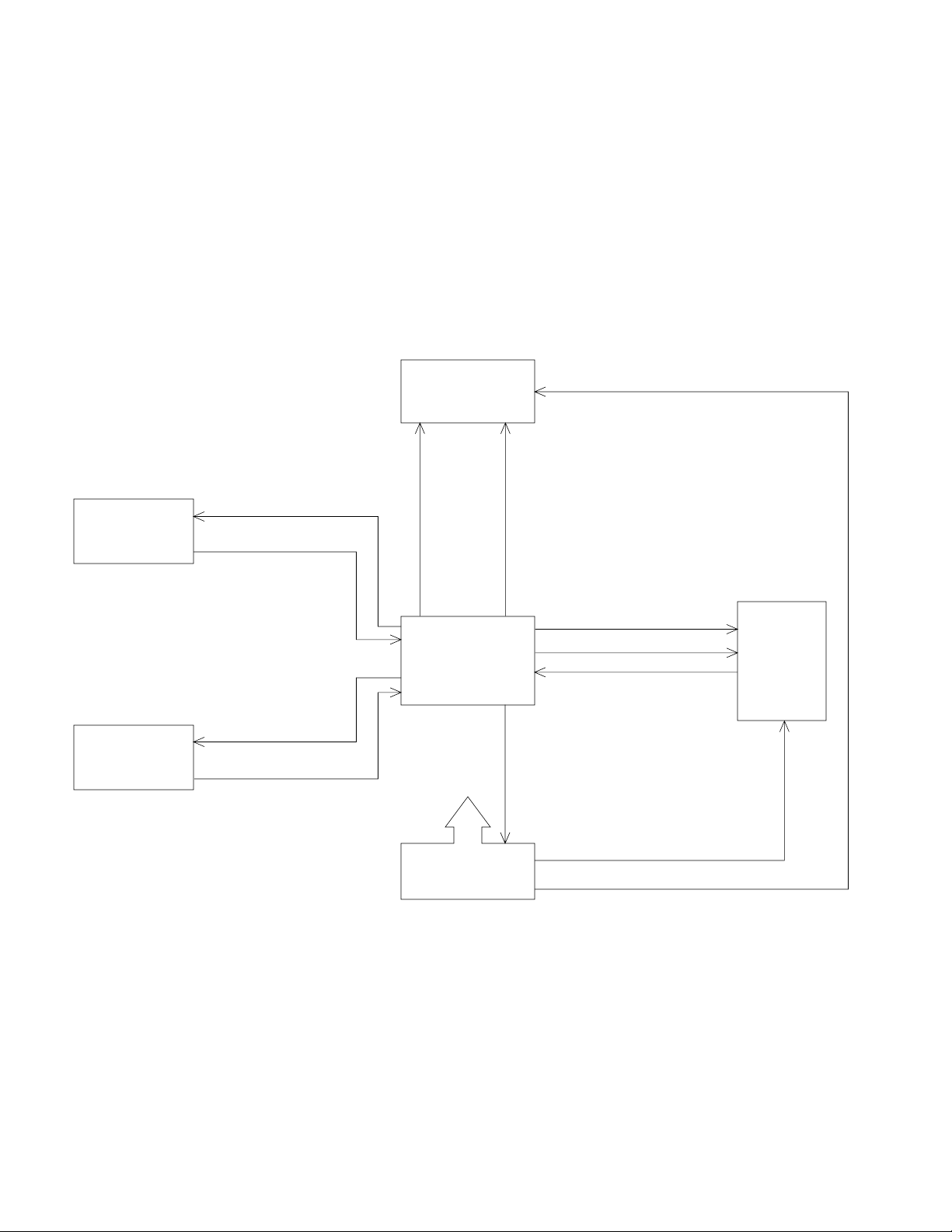
2. BLOCK DIAGRAM
Slide switch
Keyboard
Sent signal
S1~S7, SAP, SDP
SO1~SO7
SI1~SI3, SI5
KO1 ~ KO8
KI1 ~ KI6
Display tube
FG138AW7
CPU
MN158418YCY
VDD, VSS
Digital signal
D1~D13
Ribbon shift signal
Character selective signal
Timing pulse
Motor control signal
VF1,VF2
Printer
M-80
VIM, VDD
Power supply
circuit
— 1 —
Page 4

3. CPU (MN158418YCY) PIN FUNCTION
Pin No. Signal I/O Function
1~7, 64 P00~P13 Out Common signal for keyboard
8~12 P20~P22, P32, P33 In Key signal from keyboard
13 IR Q In Timing pulse signal from printer
14 DEBIN In Reset pulse (Not used)
15 IRQCNT In Auxiliary timing (VDD)
16 P40 Out Motor control signal
17 P41 Out Ribbon shift signal for printer
18~30 P42, P43, P50~P53, Out Character selective signal for printer
P70~P73, P80~P82
31, 32 P83, P90 O ut Segment signal for display,
Character selective signal for printer
33~39 P91~P93 Out Common signal for slide switch,
PA0~PA3 Segment signal for display
40 P60 In Input port (VDD)
41~43 P61~P63 In Signal from slide switch
44~56 PB0~PB3, Ou t Digit signal for display
PC0~PC3,
PD0~PD3,
PE0
57 VPP In GND terminal
58 VDD In VDD terminal (+33V)
59, 60 OSC1, OSC2 I/O Clock signal for CPU
61 VSS In VSS terminal (+28V)
62 SYNC — Not used
63 RST In Signal from slide switch, Reset signal
— 2 —
Page 5

4. DIAGNOSTICS
STEP
1
2
3
4
5
6
7
8
9
10
11
12
13
14
15
MODE SWITCHES
ON F 6
ON F 6
ON F 6
ON F 6
ON CUT 6
ON CUT 6
ON CUT 6
ON CUT 4
ON UP 3
ON 5/4 2
ON 5/4 1
ON 5/4 0
ON 5/4 ADDX
ON 5/4 ADDX
PRINT 5/4 ADDX
OPERATION
1 00 TM
C
8 – ÷ 9 % ◊/#
▲
CA
• 1 2 3 4 5 6 7
M+
M+
M–
÷ 5 MU/MD
+
=
+
=
M◊
M❊
CA 1 ÷ ÷ 1 M
DISPLAY
100°
-88.8888888888
-88.888888888
0.1234567
M 0.123456
M 0.1234
M 0.124
M 0.12
M 0.1
M 0.
M 0.123
0.123
M 0.01'
K
PRINT
0.
[-]
[88.8888888888]
0.
0 • 01 ÷
0 • 01M+
NOTE
The character with
"[ ]" will be printed
by red ink.
• • 0 • •
1 • ÷
1 • K÷
1 • =
PRINT 5/4 ADD+
16
PRINT 5/4 ADD+
17
18
ITEM+ 5/4 ADD+
ITEM+/– 5/4 ADD+
19
ITEM+/– 5/4 ADD+
20
ITEM+/– 5/4 ADD+
21
22
ITEM+/– 5/4 ADD+
ITEM+/– 5/4 ADD+
23
24
ITEM+/– 5/4 ADD+
X 1 – 1 –
◊/#
◊/#
–
IT
❊
G❊
FEED
M❊ AC
— 3 —
M -0.02
M -0.02
M -0.02
M -0.03
M 001
M -0.03
M -0.03
0.
0 • 01 X
[- 1 • =]
[- 0 • 01 +]
[0 • 01-]
[0 • 01-]
[- 0 • 02 ◊]
002
[- 0 • 02◊]
[-0 • 01-]
001
001
[- 0 • 03 G❊]
001
[- 0 • 03 G❊]
Paper feeding
001
0 • 01M❊
• • 0 • •
Press the button 2
or 3 seconds
continuously.
Page 6
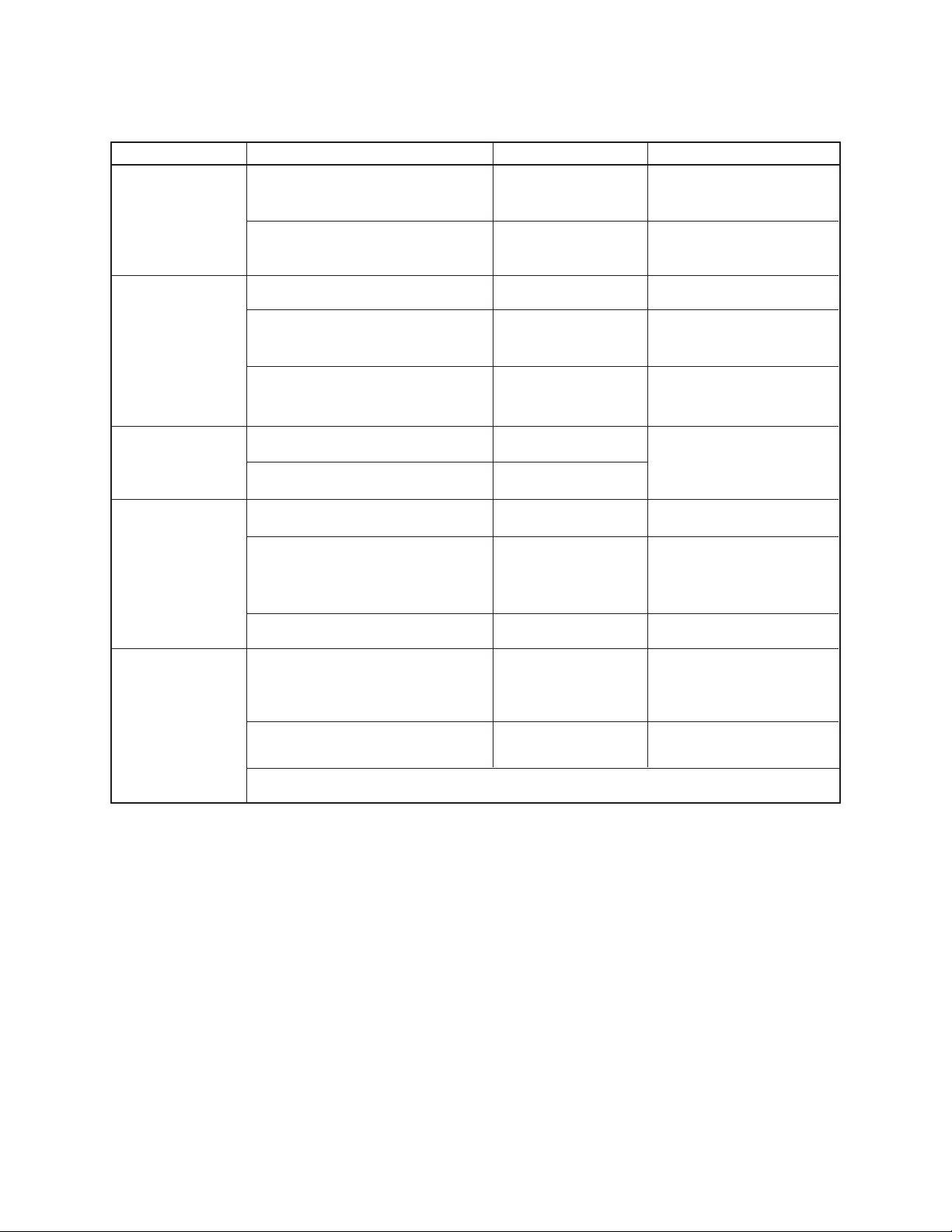
5. TROUBLESHOOTING
Trouble Cause Checkpoint Note
1) Does not work
at all.
•Defective power transformer
Secondary voltage
of transformer
VDD, VSS, VM, VF1, and
VF2 are OK?
2) No display.
3) No print.
4) Poor display.
5) Poor printing
• Motor does
not stop.
•Defective LSI
•No voltage at VF1, VF2
•No digit signal or no segment
signal
•Defective display tube
•Poor voltage VM
•Defective motor
•Defective LSI
•Short or open circuits between
digit signals and segment signals.
•Defective display tube
•Timing signal is bad.
Waveforms of each
pin
VF1, VF2
Signal D1 ~
S1 ~
Between LSI and
display tube
Check the pulse signals
from LSI.
If VF1, VF2, Digit and
Segment signals are OK.
VM=17V (while printing)
Check detector of printer
block and timing signal.
• Missing of
digits.
•Defective printer magnet
•Refer to the printer service manual published separately.
— 4 —
Page 7

6. DISASSEMBLY VIEW
21
8
7
20
6
5
— 5 —
17
12
16
15
10
13
23
14
9
11
19
26
18
4
3
2
1
19
22
Voltage
100V
120V
220V
240V
25
Connection
Power Cord
Projection side
Black
Projection side
Marking side
Brown
Blue
Brown
Blue
Transformer
Yellow
Black
Blue
Black
Black
White
Black
24
Red
Page 8

7. SCHEMATIC DIAGRAM
7-1. Main board
— 6 —
Page 9

7-2. Keyboard
KO1
KO2
KO3
KO4
KO5
KI1
KI2
FEED
/
–
9
8
X
6
5
KI3
/ #
+
3
2
KI4
G*
KI5
.
0
IT
KI6
00
000
KO6
KO7
KO8
M
CA
M
4
— 7 —
1
%
M–
C
MU/MD
M+
TIME
7
Page 10

7-3. Slide Switch Board
VSS SI5
OFF
ON
SI3
PON
IT+
IT–
F
SI2
CUT
UP
5/4
SO1
6
SI1
SO2
SO3
SO4
SO5
SO6
SO7
4
3
2
1
0
ADDX
ADD+
MODE SWITCH
— 8 —
Page 11

7-4. Printer Pin Arrangement Diagram
Connection Pin No. ConnectionPin No.
RD terminal
1
Character selective
15
magnet column No.1
(Not used)
Character selective
magnet column No.1
2
3
4
5
6
7
8
9
10
10
11
12
2
3
4
16
17
18
13
14
15
Notes:
1. Column numbers match
5
19
16
the physical arrangement of the columns on
the print wheels.
6
20
17
2. Column numbers are assigned from 1 to 18 from
Ribbon shift magnet
7
21
the frame motor side.
3. Pin numbers are assigned from 1 to 27 from
8
22
Electromagnet (+)
the frame motor side.
4. The spark arrestor diode
is connected as shown
9
M
23
Motor power
supply (+)
24
Detector power
supply (+)
Timing signal
25
Detector power
26
supply (–)
below.
Electromagnet (+) Driver
(Example of compatible diode:
1S2075K or equivalent)
Motor power
11
13
27
supply (–)
14
12
Motor power ON/OFF
Timing signal
Character selective magnet No.n
T0 T1 T2 T3 T4 T5 T6 T7 T8 T9 T10 T11 T12
*2
8.0ms min. 2.0ms min.
0.7ms max.0.7ms max.
0.7ms max.0.7ms max. 80.0ms min.
8
0.2ms max.
*1
TS T(0)
Ribbon shift magnet
(Print operation)
(Normal paper feeding operation)
Typ. 285.7ms
Notes:
1. The signals in must be prepared by the user.
2. The pulse is indicated by a dot-dash line (*1) is generated for continuous printing. The next print cycle can start
immediately after the leading edge of the timing signal Ts.
3. As shown by a dashed line (*2), the timing signal may go low at motor power-on or upon reception of a Print command.
— 9 —
Page 12

8. PARTS LIST
FOB Japan
N Item Code No. Parts Name Specification Quantity M N.R.Yen R
A B C Unit Price
PCB L224-1 ASS'Y
N LSI 2012 1295 LSI MN158418YCY 1
IC1, 2 2114 2436 Mos IC BA12003 2
Q1 2251 0525 Transistor 2SB1329-Q,R 1
Q3, 4 2252 0896 Transistor 2SC1740S-R,S 2
Q5 2250 0672 Transistor 2SA933S-R,S 1
Q6 2251 0581 Transistor 2SB1374-Q,R 1
Q7, 8 2259 1449 Digital transistor DTD114ES 2
D1~5 2390 0378 Diode 1SR139-100T-32-T 5
D6~8 2360 1946 Zener diode MTZJ5.6CT-77-T 3
D9~11 2301 0054 Diode 1S2472-T-77-T 3
D13, 14 2301 0101 Diode 1S2473-T-77-T 2 2 2 20 C
The following elecrical parts will be not supplied from CASIO.
C1, 8 Semiconductive capacitor 0.1uF, 50V, +20/-80% 2
C2 Electrolytic capacitor 330uF, 50V 1
C4 Ceramic capacitor 1pF, 50V, ±10% 1
C5 Electrolytic capacitor 10uF, 16V 1
C6 Semiconductive capacitor 0.22uF, 12V, +20/-80% 1
C7 Ceramic capacitor 10pF, 50V, ±5% 1
C9,10 Ceramic capacitor 0.01uF, 50V, +20/-80% 2 2 2
R1 Carbon film resistor 6.8Kohm, 1/2W, ±5% 111
R2 Carbon film resistor 3.9Kohm, 1/2W, ±5% 111
R5 Carbon film resistor 3.3Kohm, 1/4W, ±5% 111
R6 Carbon film resistor 15Kohm, 1/4W, ±5% 111
R7 Carbon film resistor 1Kohm, 1/4W, ±5% 111
R8 Carbon film resistor 3.6Kohm, 1/4W, ±5% 111
R9 Carbon film resistor 470ohm, 1/4W, ±5% 111
R10 Carbon film resistor 270ohm, 1/4W, ±5% 111
R11 Carbon film resistor 390ohm, 1/4W, ±5% 111
R12 Carbon film resistor 5.1Kohm, 1/4W, ±5% 1
R13 Carbon film resistor 20ohm, 1/2W, ±5% 1
R14 Carbon film resistor 6.8Kohm, 1/4W, ±2% 1
R15 Carbon film resistor 200ohm, 1/4W, ±5% 1
R17~19 Metal film resistor 100ohm, 1W, ±5% 3
11 1
22 5
1110
2220
1120
1110
2220
5520
3320
3320
22
11
11
11
11
11
11
11
11
11
33
B
B
B
B
B
B
B
C
C
C
N 1 6055 1760 PCB L224-1 Ass'y P240033A*1HK 1
(This ass'y contains the above parts as its element.)
PCB UNIT
N 1 6055 1760 PCB L224-1 Ass'y P240033A*1HK 1
2 3301 0217 Display tube FG138AW7 1
3 6053 7440 PC joiner B-V298 P310141-4 1
N 4 1014 8290 Digital printer M-80-021 1
N C3 2803 8199 Electrolytic capacitor RE2-25V222M-T50 1
Notes: N – New parts Essential
M – Minimum order/supply quantity Stock recommended
R – Rank Others
Q – Quantity used per unit No stock recommended
R – A :
B :
C :
D :
— 10 —
A : DR-120XA
B : DR-320A
C : DL-220BAGY
11 1
11 1
11 1
11 5
11 1
11 5
B
B
A
C
A
C
Page 13

FOB Japan
N Item Code No. Parts Name Specification Quantity M N.R.Yen R
A B C Unit Price
Q2 2253 0469 Transistor 2SD1380-QR 1
COMPONENTS
11 5
C
5 6053 7260 Upper case V298 P110127-1 0
5 6053 7770 Upper case V298B (Gray) P110127-2 1
5 6053 8960 Upper case V298C (White) P110127-3 1
6 6053 7270 Printer cover V298 P210316-1 0
6 6053 7780 Printer cover V298B (Gray) P210316-2 1 1 0 10 C
6 6053 8980 Printer cover V298B (White) P210316-3 1 0 0 10 C
7 6053 7280 Ten key ass'y P310315*1 1 1 1 1 C
8 6053 7290 Function key ass'y P210321*1 1
9 6052 6620 Hang A-V282 P410126-2 1
10 6052 6630 Hang B-V282 P410117-2 1
11 6052 6640 Hang C-V282 P410127-2 1
12 6053 7300 Key rubber V298 P110124-1 1
13 6053 7330 Switch knob V298 P310312-1 0
13 6053 7810 Switch knob V298B (Gray) P310312-2 3
13 6053 8900 Switch knob V298C (White) P310312-3 3
14 6329 8310 Switch spring G310 A45208-1 6
15 6053 7340 Common film V298 P310302-1 1
16 6053 7350 Spacer V298 P310314-1 1
17 4311 5890 PCB-V298-E4 (Keyboard) P210310-1 1
18 6053 7360 PC joiner A-V298 P310141-3 1
19 6389 3307 Printer cushion M4K3791 4
20 6053 7390 Paper cutter V298 P310311-1 1
N 21 6055 1951 Display panel L224B P210317A-10 0
N 21 6055 1961 Display panel L224C P210317A-11 1
N 21 6055 2151 Display panel L224I P210317A-14 0
22 6053 7400 Lower case V298 P110128-1 0
22 6053 7410 Lower case V298B (Gray) P110128-2 1
22 6053 8930 Lower case V298C (White) P110128-3 1
23 3701 0308 Power cord (USA/CANADA) SPT-2-1B-C 1
23 3701 0329 Power cord (Europe) CLASS2-AB-2 1
23 3701 0322 Power cord (U.K.) BX-103-J02 0
23 3701 0546 Power cord (Australia) SP-852-J02 1
24 5530 0526 Terminal connector CE2 2
25 3680 1131 Terminal cap 2.0DUL 1
N 26 3012 1344 Power transformer SE-223-1D1J 1
N 26 3012 1351 Power transformer SE-223-1D2 1
01 1
10 1
00 1
0110
11 1
11 1
11 1
11 1
11 1
03 1
30 1
00 1
6620
1120
11 5
1110
11 1
4410
1110
10 5
00 5
01 5
01 1
10 1
00 1
01 1
10 1
10 1
00 1
2210
1110
01 1
00 1
X
X
X
C
C
X
X
X
C
C
C
C
C
B
X
B
C
X
B
C
C
C
X
X
X
C
C
C
C
X
X
B
B
OTHERS
3613 1043 Plug (U.K) NTA750(3A) 0
6053 4450 Roll arm L-V985 P310270-1 0
6053 4460 Roll arm R-V985 P310269-1 0
6053 5810 Roll arm L-V985B (Gray) P310270-2 1
6053 5820 Roll arm R-V985B (Gray) P310269-2 1
6053 9050 Roll arm L-V298C (White) P310270-3 1
6053 9060 Roll arm R-V298C (White) P310269-3 1
Notes: N – New parts Essential
M – Minimum order/supply quantity Stock recommended
R – Rank Others
Q – Quantity used per unit No stock recommended
R – A :
B :
C :
D :
— 11 —
10 1
0110
0110
1010
1010
0010
0010
A : DR-120XA
B : DR-320A
C : DL-220BAGY
X
A
A
A
A
A
A
Page 14

8-11-10, Nishi-Shinjuku
Shinjuku-ku, Tokyo 160, Japan
Telephone: 03-3347-4926
 Loading...