

Page 1
CPS-7
(with price)
ELECTRONIC KEYBOARD
CPS-7
Page 2

CONTENTS
Specifications . . . . . . . . . . . . . . . . . . . . . . . . . . . . . . . . . . . . . . . . . 2
Block Diagram . . . . . . . . . . . . . . . . . . . . . . . . . . . . . . . . . . . . . . . . . 3
Circuit Description . . . . . . . . . . . . . . . . . . . . . . . . . . . . . . . . . . . . . 4
Major Waveforms . . . . . . . . . . . . . . . . . . . . . . . . . . . . . . . . . . . . . . 8
PCB View and Check Points . . . . . . . . . . . . . . . . . . . . . . . . . . . . . 9
Schematic Diagrams. . . . . . . . . . . . . . . . . . . . . . . . . . . . . . . . . . . 10
Exploded View. . . . . . . . . . . . . . . . . . . . . . . . . . . . . . . . . . . . . . . . 12
Parts List . . . . . . . . . . . . . . . . . . . . . . . . . . . . . . . . . . . . . . . . . . . . 13
SPECIFICATIONS
GENERAL
Number of keys: 76
Polyphonic: 24-note
Preset tones: 5, Piano-1, Piano-2, Electric Piano, Pipe Organ, Strings
Layer
Touch response: On/Off
Key transpose: Range of ± 1 octave by a semitone increment
Demo tunes: 5, 1. Petit Chien
2. Cozy's Castle
3. Red Leaves
4. Toccata & Chorus
5. Rainbow
Tuning control: 440Hz ± 50 cents
Built-In speakers: 12 cm dia. 5 W input rating: 2 pcs.
MIDI: 8-channel, multi-timbral reception
Terminals: Phone Jack [Output impedance: 47 Ω, Output voltage: 2.6 V(rms) MAX],
MIDI Jacks (IN, OUT), Sustain Jack, AC Adaptor Jack (12 V)
Auto power off: Approximately 6 minutes after the last operation
Power source: 2-way AC or DC source
AC: AC adaptor AD-12
DC: 6 D size dry batteries
Battery life: approx. 4 hours by manganese batteries R20P/SUM-1
Power consumption: 18 W
Dimensions (HWD): 96 x 1161 x 303 mm (3-3/4 x 45-11/16 x 11-15/16 inches)
Weight: 6.3 kg (13.9 lbs) excluding batteries
ELECTRICAL
Current Drain with 12 V DC:
No Sound Output 145 mA ± 20%
Maximum Volume 1470 mA ± 20%
with keys C2 to B3 (24 polyphonic) pressed in Strings tone
Volume: maximum, Touch response: maximum
Headphone Output Level (Vrms with 8 Ω load each channel):
with key F3 pressed in Strings tone Left channel 100 mV ± 20%
Speaker Output Level (Vrms with 8 Ω load each channel):
with key F2 pressed in Strings tone Left channel 2800 mV ± 20%
Minimum Operating Voltage: 5.8 V
— 2 —
Page 3
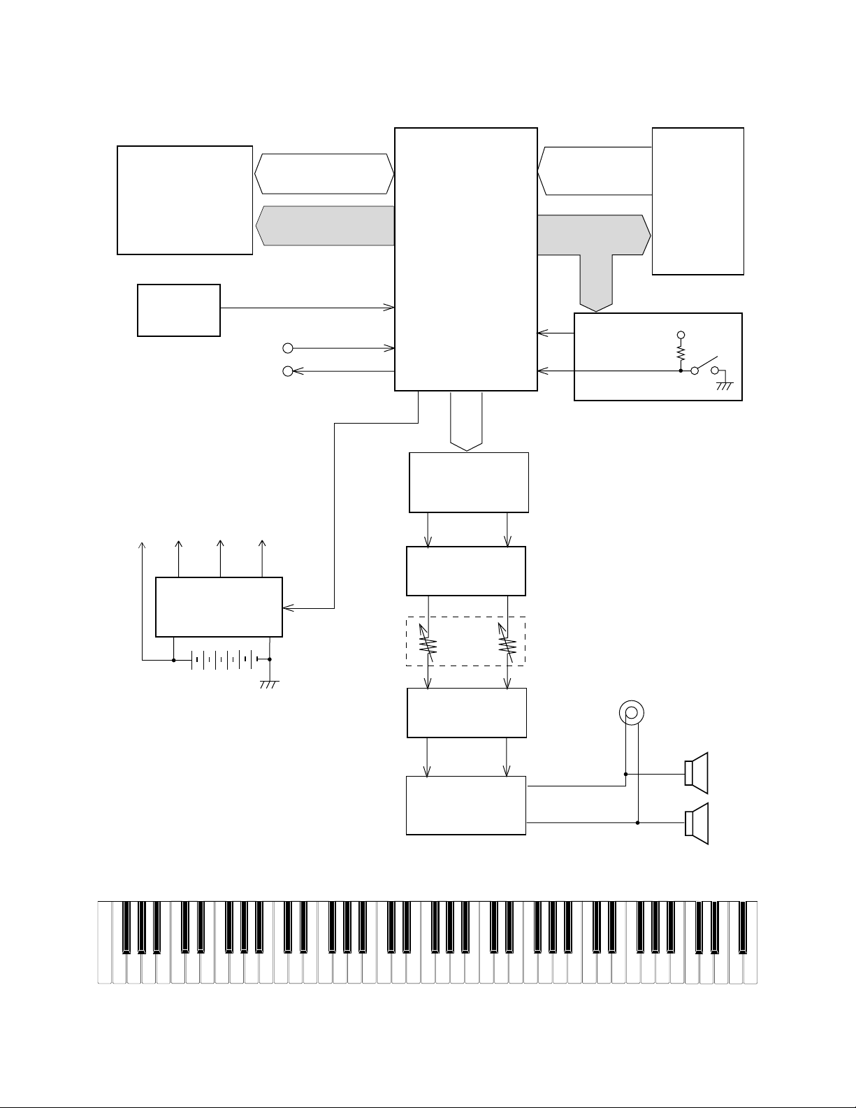
BLOCK DIAGRAM
Sound Source ROM
(2M-bit)
LSI102
TC534200CF-C116
Reset IC
IC106
RE5VA35AA
MIDI
VCC
AVDD
VC
Power Supply Circuit
Q102 ~ Q107,
D105, D106
RESET
IN
OUT
VDD
MD0 ~ MD15
MA0 ~ MA17
APO
CPU
LSI101
UPD912GF-3BA
LRCK, SO, BCK
D/A Converter
IC105
UPD6379GR
Filter
IC104
M5218APR
Main
Volume
KI0
NMI
FI0 ~ FI9
SI0 ~ SI9
KC0 ~ KC7
Buttons
Keyboard
VDD
Power Switch
NOMENCLATURE OF KEYS
F#1 G#1 A#1
E1 F1 G1 A1 B1
C#2
C2 D2E2F2G2A2 B2 C3 D3
F#2D#2
C#3A#2G#2
D#3
E3
Equalizer
IC103
M5218APR
Power Amplifier
IC101
LA4620
F#3 G#3
A#3 C#4 D#4
F3 G3 A3 B3 C4 D4 E4 F4 G4 A4 B4 C5 D5 E5 F5 G5 A5 B5
F#4 G#4
C#5
A#4
D#5
F#5 G#5
A#5
— 3 —
Output
Speakers
C#6
C6
G#6F#6D#6
A#6
B6A6G6F6E6D6
C#7 D#7 F#7
C7
D7 E7 F7 G7
Page 4
CIRCUIT DESCRIPTION
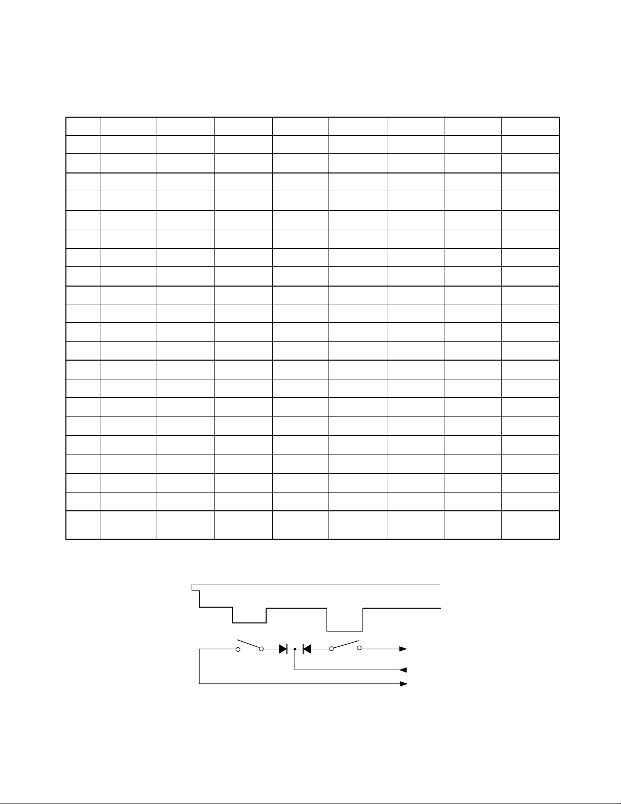
KEY MATRIX
KC0 KC1 KC2 KC3 KC4 KC5 KC6 KC7
FI0 E1 (1) F1 (1) F#1 (1) G1 (1) G#1 (1) A1 (1) A#1 (1)
SI0 E1 (2) F1 (2) F#1 (2) G1 (2) G#1 (2) A1 (2) A#1 (2)
FI1 B1 (1) C2 (1) C#2 (1) D2 (1) D#2 (1) E2 (1) F2 (1) F#2 (1)
SI1 B1 (2) C2 (2) C#2 (2) D2 (2) D#2 (2) E2 (2) F2 (2) F#2 (2)
FI2 G2 (1) G#2 (1) A2 (1) A#2 (1) B2 (1) C3 (1) C#3 (1) D3 (1)
SI2 G2 (2) G#2 (2) A2 (2) A#2 (2) B2 (2) C3 (2) C#3 (2) D3 (2)
FI3 D#3 (1) E3 (1) F3 (1) F#3 (1) G3 (1) G#3 (1) A3 (1) A#3 (1)
SI3 D#3 (2) E3 (2) F3 (2) F#3 (2) G3 (2) G#3 (2) A3 (2) A#3 (2)
FI4 B3 (1) C4 (1) C#4 (1) D4 (1) D#4 (1) E4 (1) F4 (1) F#4 (1)
SI4 B3 (2) C4 (2) C#4 (2) D4 (2) D#4 (2) E4 (2) F4 (2) F#4 (2)
FI5 G4 (1) G#4 (1) A4 (1) A#4 (1) B4 (1) C5 (1) C#5 (1) D5 (1)
SI5 G4 (2) G#4 (2) A4 (2) A#4 (2) B4 (2) C5 (2) C#5 (2) D5 (2)
FI6 D#5 (1) E5 (1) F5 (1) F#5 (1) G5 (1) G#5 (1) A5 (1) A#5 (1)
SI6 D#5 (2) E5 (2) F5 (2) F#5 (2) G5 (2) G#5 (2) A5 (2) A#5 (2)
FI7 B5 (1) C6 (1) C#6 (1) D6 (1) D#6 (1) E6 (1) F6 (1) F#6 (1)
SI7 B5 (2) C6 (2) C#6 (2) D6 (2) D#6 (2) E6 (2) F6 (2) F#6 (2)
FI8 G6 (1) G#6 (1) A6 (1) A#6 (1) B6 (1) C7 (1) C#7 (1) D7 (1)
SI8 G6 (2) G#6 (2) A6 (2) A#6 (2) B6 (2) C7 (2) C#7 (2) D7 (2)
FI9 D#7 (1) E7 (1) F7 (1) F#7 (1)
G7 (1)
SI9 D#7 (2) E7 (2) F7 (2) F#7 (2) G7 (2)
KI1
Touch
Response
Transpose
/Tune/MIDI
Piano-1 Piano-2 E.Piano
Pipe
Organ
Strings Demo
Note: Each key has two contacts, the first conatct (1) and second contact (2).
Key
FI
Second contact (2)
First contact (1)
KC
SI
— 4 —
Page 5
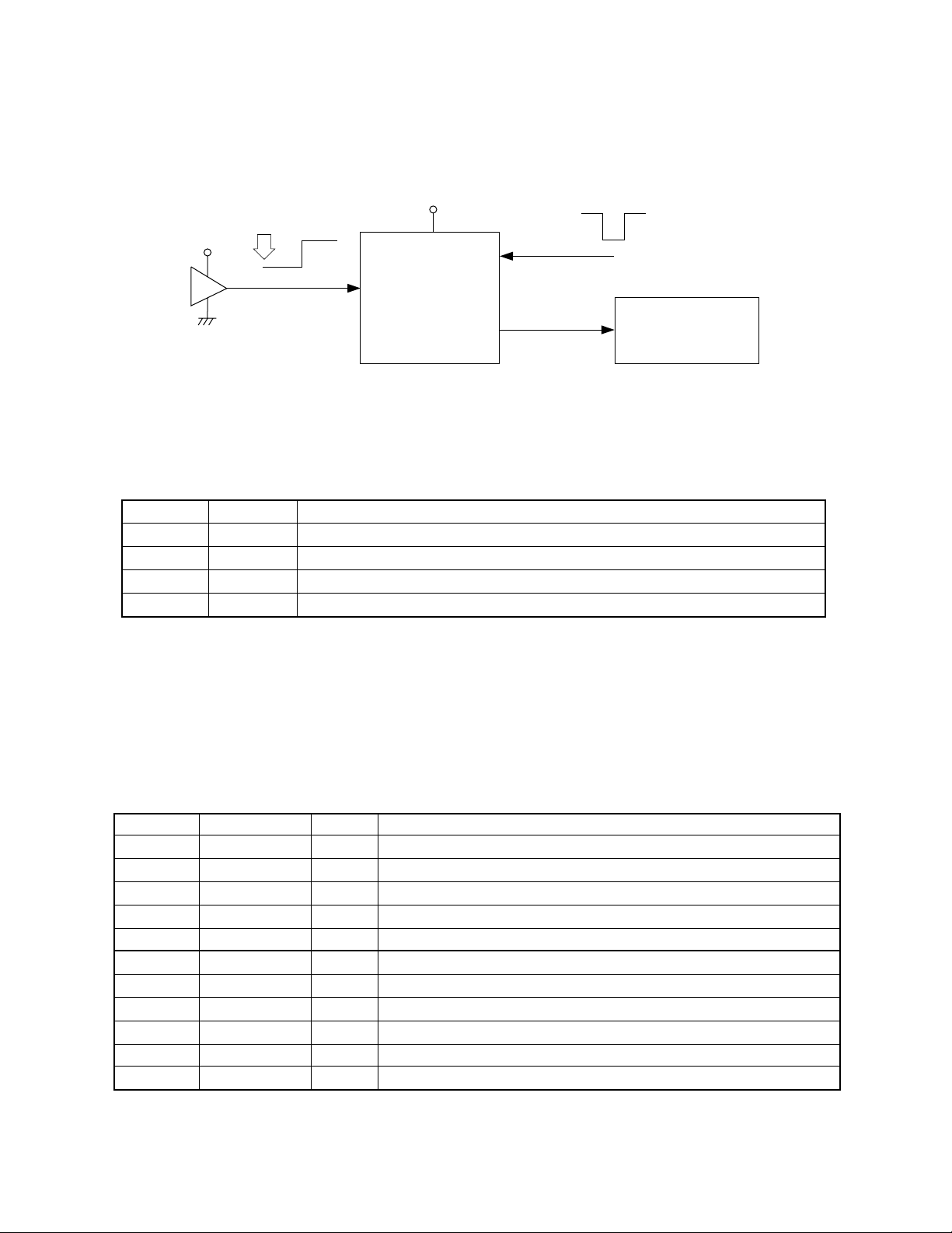
RESET CIRCUIT
When batteries are set or an AC adapter is connected, the reset IC provides a low pulse to the CPU. The CPU
then initializes its internal circuit.
When the power switch is pressed, the CPU receives a low pulse of POWER signal.The CPU raises APO
signal to +5 V to turn power on.
VDD
CPU
LSI101
SCKO
POWER
APO
From power switchNMI
Power Supply Circuit
VDD
Battery set
RESET
Reset IC
IC106
RE5VA35AA
RSTB
UPD912GF-3BA
POWER SUPPLY CIRCUIT
The power supply circuit generates four voltages as shown in the following table. VDD voltage is always
generated. The others are controlled by APO signal from the CPU.
Name Voltage For operation of
VDD +5 V CPU, Reset IC, Sound source ROM
AVDD +5.3 V DAC
AVCC +12 V Filter block, Equalizer block
VC +12 V Power amplifier
CPU (LSI101: UPD912GF-3BA)
The 16-bit CPU contains a 1k-byte RAM, three 8-bit I/O ports, two timers, a keycontroller and serial interfaces.
The CPU detects key velocity by counting the time between first-key input signal FI and second-key SI from
the keyboard. The CPU read sound data and velocity data from the sound source ROM in accordance with
the selected tone. Then the CPU provides 16-bit serial sound data to the DAC.The CPU also controls MIDI
input/output and LED driving.
The following table shows the pin functions of LSI101.
Pin No. Terminal In/Out Function
1 TXD0 Out MIDI signal input
2 RXD0 In MIDI signal output
3 SCK0 Out APO (Auto Power Off) signal output
4 ~ 6 — Not used. Connected to ground.
7 AVCC In Ground (0 V) source
8, 9 AN0, AN1 — Not used. Connected to ground.
10 AGND In Ground (0 V) source
11 BCK Out Bit clock output
12 SO Out Serial sound data output
13 LRCK Out Word clock output
14 GND In Ground (0 V) source
— 5 —
Page 6

Pin No. Terminal In/Out Function
15, 16 XLT0, XLT1 In/Out 20 MHz clock input/output
17 VCC In +5 V source
18, 19 MD0, MD1 In Mode selection terminal. Connected to ground.
20 RSTB In Reset signal input
21 NMI In Power ON signal input
22 INT — Not used. Connected to ground.
23 ~ 30
FI0 ~ FI3
SI0 ~ SI3
In Key input signal
31 ~ 38 KC0 ~ KC7 Out Key scan signal output
39 ~ 50
FI4 ~ FI9
SI4 ~ SI9
In Key input signal
51 FI10 In Not used
52 SI10 In Not used
53 KI0 In Button input signal input
54 KI1 — Not used
55 KI2 Out LED drive signal
56 ~ 58 — Not used
59 ~ 76 MA1 ~ MA18 Out Address bus
77 MCSB0 Out Chip enable signal output for the sound source ROM
78, 79 — Not used
80 VCC In +5 V source
81 GND In Ground (0 V) source
82 MRDB Out Read enable signal output for the sound source ROM
83 ~ 98 MD0 ~ MD15 In/Out Data bus
99 PLE In Sustain signal input
100 P17 In APO cancellation signal input
Block diagram of digital circuits
Sound Source ROM
TC534200CF-C116
CE
MSB0
From keyboard
FI0 ~ FI9
SI0 ~ SI9
PG
X101
20 MHz
UPD912GF-3BA
LSI102
A0 ~ A17 D0 ~ D15
MA1 ~
MA18
MD0 ~
MD15
CPU
LSI101
— 6 —
SO: Sound data
BOK: Bit clock
LRCK: Word clock
SO
BOK
LRCK
SI
CLK
LRCK
UPD6379GR
DAC
IC105
ROUT
LOUT
Page 7

DAC (IC105: UPD6379GR)
The DAC receives 16-bit serial data output from the CPU. The data contains digital sound data of the melody,
chord, bass, and percussion for the right and left channels. The DAC converts the data into analog waveforms
and output them to each channel separately.
FILTER BLOCK
Since the sound signals from the DAC are stepped waveforms, the filter block is added to smooth the
waveforms.
Filter Block
To main volume
IC104
From DAC
EQUALIZER BLOCK
The equalizer block boots low frequencies to compensate for the reduced response of the built-in speakers.
Equalizer Block
To power amplifier
IC103
POWER AMPLIFIER (IC102: LA4598)
The power amplifier is a two-channel amplifier with standby switch.
+
3
IN11+
IN11-
IN12-
PriGND
IN21+
IN21-
IN22-
5
4
6
9
7
8
Input
Amp.
-
Input
Amp.
+
Terminal
Protection
Circuit
+
Input
Amp.
-
Input
Amp.
+
16
NC DC MUTE VCC2 ADJ
Pre-drive
Amp.
RL Short
Protector
Pre-drive
Amp.
Pre-drive
Amp.
RL Short
Protector
Pre-drive
Amp.
2
10
Ripple
Filter
Power
Amp.
Power
Amp.
Power
Amp.
Power
Amp.
11
Pop Noise
Prevention
Circuit
13
From main volume
Boot11
19
OUT11
20
PoGND1
21
OUT12
22
23
Boot21
1
VCC1
18
Boot21
OUT21
17
PoGND2
15
OUT22
14
12
Boot22
— 7 —
Page 8
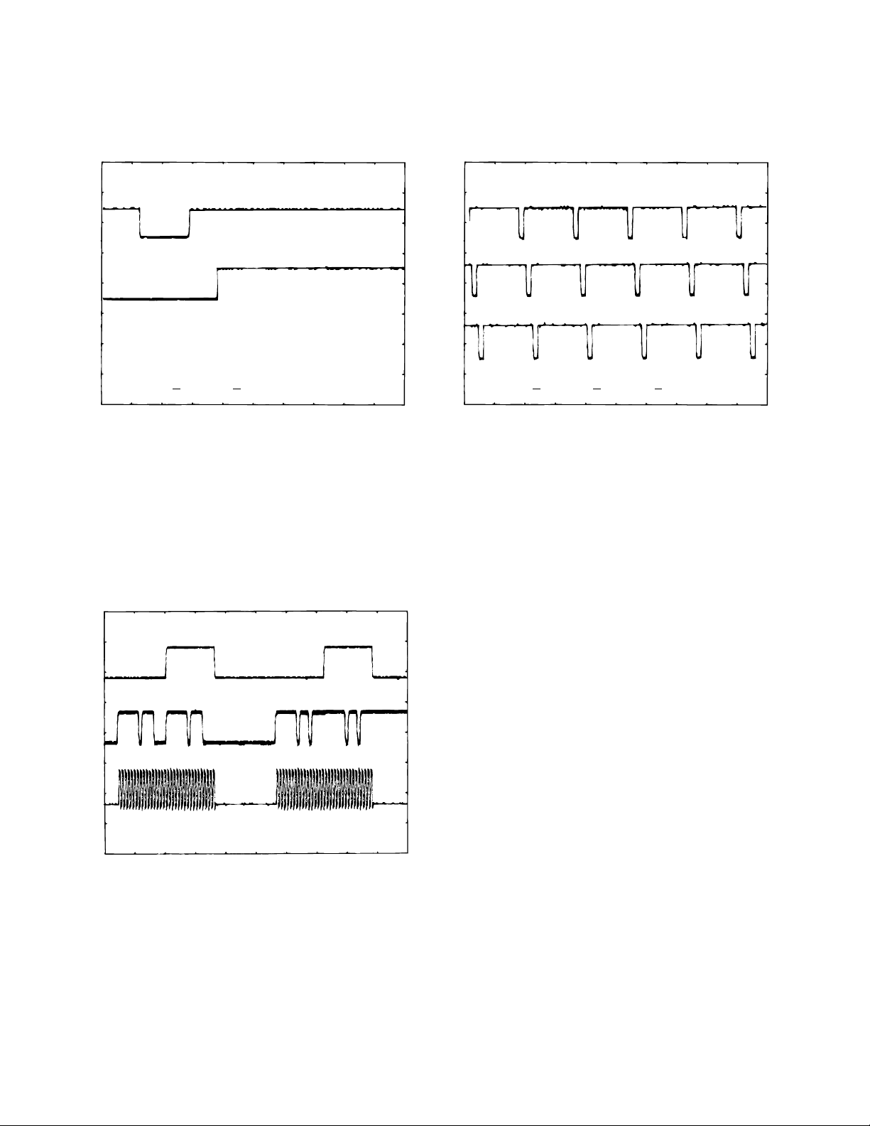
MAJOR WAVEFORMS
1
2
CH1: CH2:
1 POWER ON signal
UPD912GF-3BA pin 21
2 APO signal
UPD912GF-3BA pin 3
0.1 s
CH1
3
50 µs
CH1
4
CH2
5
5 V5 V
CH1: CH2:
5 V5 V CH3: 5 V
3 Key scan signal KC0
UPD912GF-3BA pin 31
4 Key scan signal KC1
UPD912GF-3BA pin 32
5 Key scan signal KC2
UPD912GF-3BA pin 33
CH2
CH3
6
7
8
–––
CH1: 5 V CH2: 5 V CH3: 5 V
6 Word clock LRCK
UPD912GF-3BA pin 13
7 Data signal SO
UPD912GF-3BA pin 12
8 Bit clock BCK
UPD912GF-3BA pin 11
A 2 µs
CH1
CH2
CH3
— 8 —
Page 9
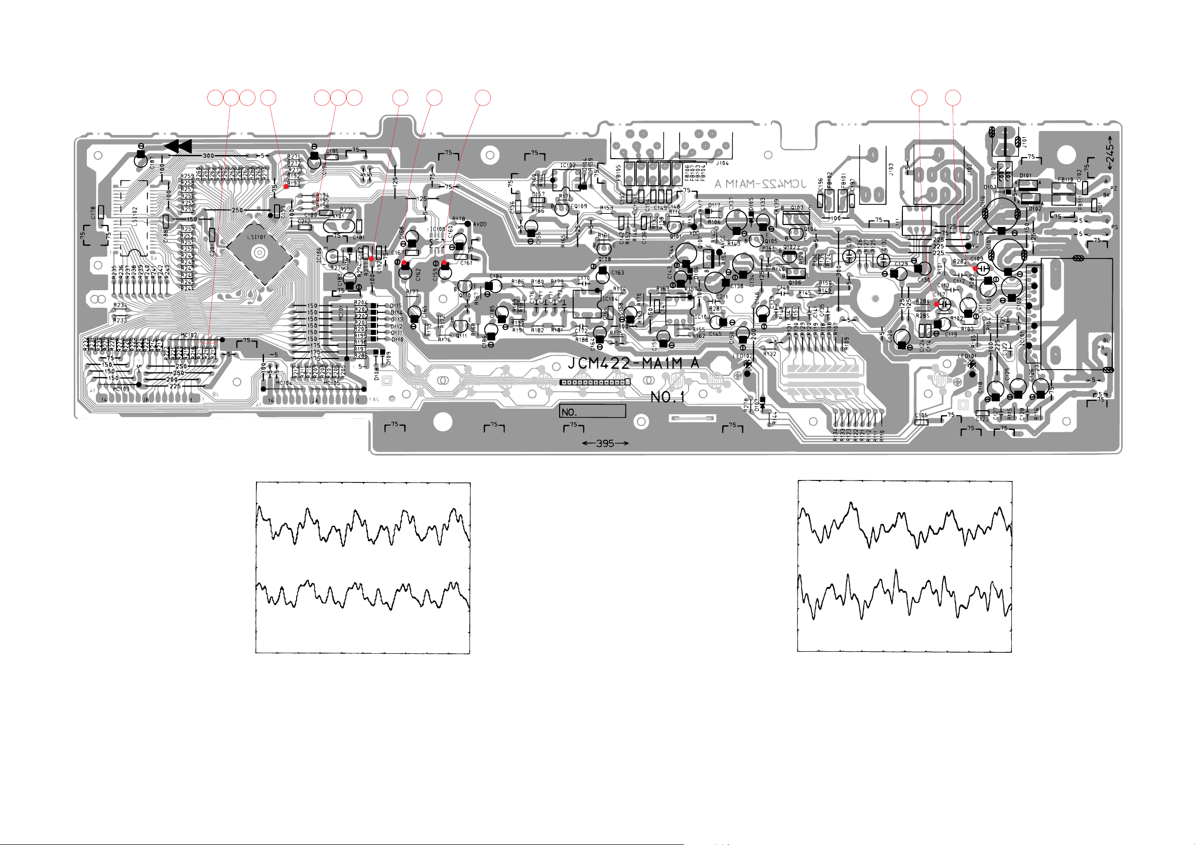
PCB VIEW AND CHECK PRINTS
6 823 4 5 7
101
12119
9
0
CH1: 0.1 V CH2: 0.1 V
9 DAC output (R-ch)
UPD6379GR pin 5
0 DAC output (L-ch)
UPD6379GR pin 8
~~
A 1 ms
CH1
CH2
Tone: Piano-1
Key: A4
Touch response: Off
Volume: Maximum
A
B
CH1: 50 mV CH2: 50 mV
A Equalizer output (R-ch)
B Equalizer output (L-ch)
~~
A 1 ms
CH1
CH2
— 9 —
Page 10
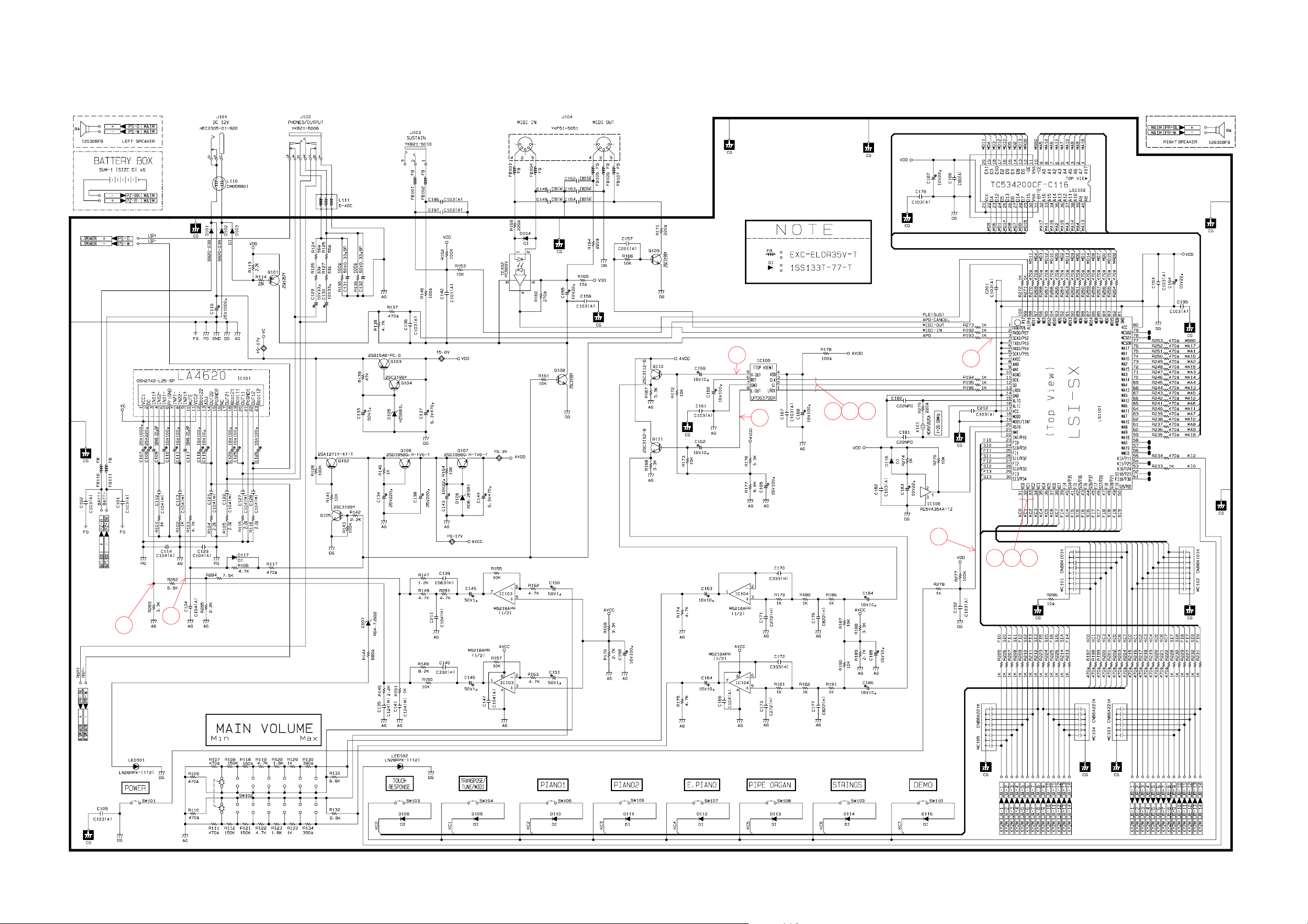
MAIN PCB JCM422-MA1M
SCHEMATIC DIAGRAMS
5.1
4.5
5.1
0.0
12
11
11.7
5.7
11.7
11.0
0.7
0.0
11.6
11.0
5.111.1
5.36.0
9
10
76 8
1
2
43 5
— 10 —
Page 11

KEYBOARD PCBs JCM762T-KY1M/KY2M
— 11 —
Page 12
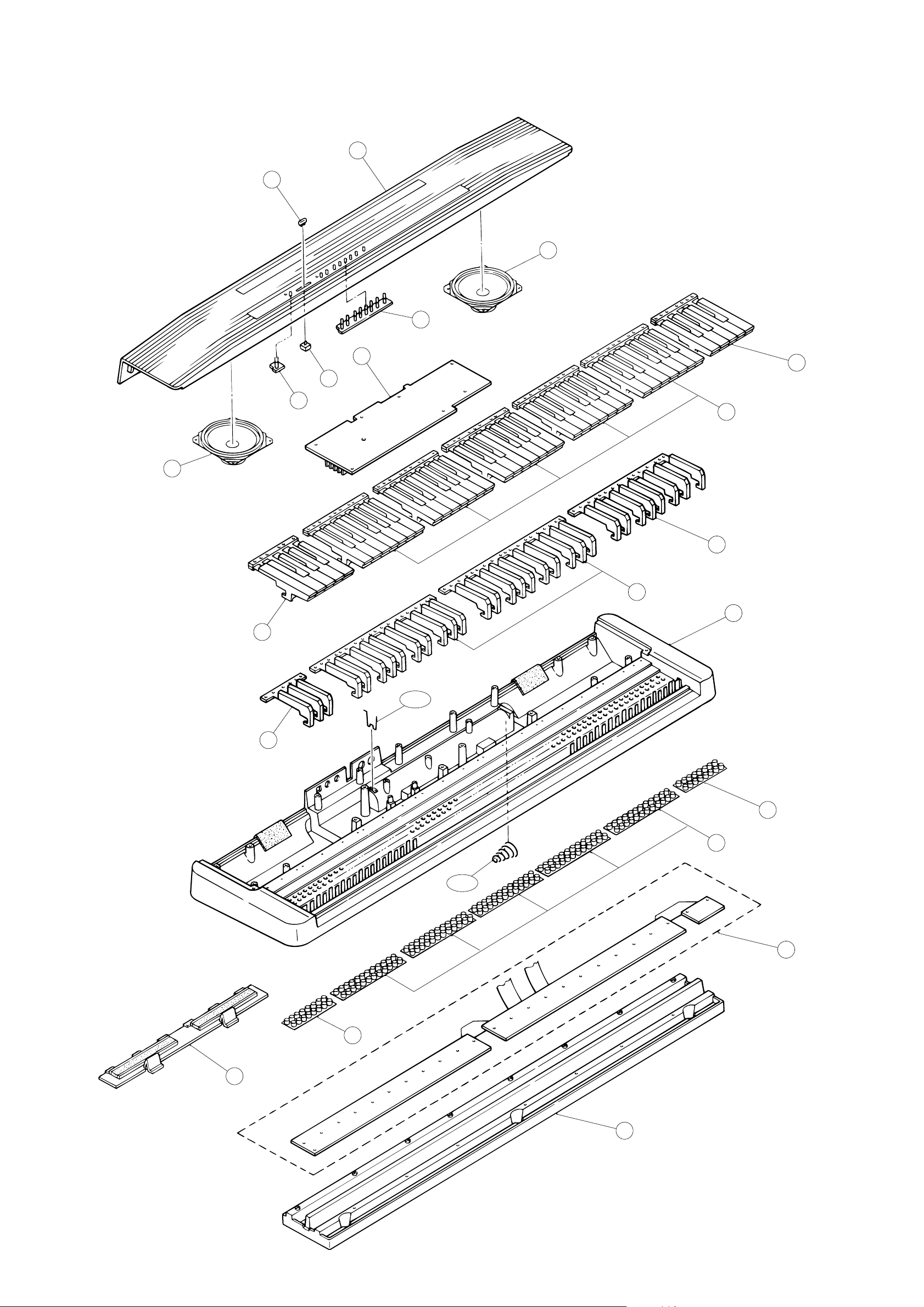
EXPLODED VIEW
8
7
3
1
4
5
6
6
9
10
12
13
15
11
14
15-1
15-2
20
18
17
16
2
19
— 12 —
Page 13

PARTS LIST
CPS-7
Notes: 1. Prices and specifications are subject to change with-
out prior notice.
2. As for spare parts order and supply, refer to the
"GUIDEBOOK for Spare parts Supply", published
seperately.
3. The numbers in item column correspond to the same
numbers in drawing.
Page 14

FOB Japan
N Item Code No. Parts Name Specification Q N.R.Yen R
Unit Price
Main PCB
N 1 6923 7620 PCB ass'y JCM422-MA1M M140249*1 1 5,530 B
LSI101 2012 0168 LSI UPD912GF-3BA 1 750 A
N LSI102 2012 1085 LSI TC534200CF-C116 1 560 A
IC105 2105 4249 LSI UPD6379GR 1 150 A
IC101 2114 1883 IC LA4620 1 350 A
IC102 2114 1421 IC, Photocoupler PC900V 1 210 B
IC103/104 2114 1799 IC M5218APR 2 54 B
IC106 2105 3941 IC RE5VA35AA-TZ 1 44 B
Q101 2200 4409 Transistor 2SA933-SQ-TP-T 1 14 A
Q102 2250 0168 Transistor 2SA854-SR-TP-T 1 20 A
Q103 2251 0672 Transistor 2SB1548-P.CS 1 44 A
Q104/105, 2220 1387 Transistor 2SC1740SQ-TP-T
Q108/109
Q106/107 2253 0448 Transistor 2SD1858Q,R-TV6-T
Q110/111 2252 0168 Transistor 2SC3112B-TPE2-T 2 15 B
D101/102 2390 1463 Schottky SB20-03B 2 39 B
D103/104, 2390 1344 Diode 1SS133T-77-T
D108~117
D105 2360 1085 Zener diode HZS6B1LTD-T 1 10 A
D106
D107 2310 7996 Zener diode RD4.7ESB2-T1-T 1 12 B
LED101/102 2370 0616
X101
J101 3501 5012 Jack, Power HEC2305-01-920 1 25 A
J102 3612 0665
J103 3612 0789 Jack YKB21-5010 1 60 B
J104 3501 4816 Jack, DIN YKF51-5051
MC101/102 2845 0168 Module capacitor CNB8X101K 2 58 C
MC103/104
MC105 2845 0049 Module capacitor CNB8X221K 1 58 C
N 2 6923 7630 PCB ass'y M762T-KY123M M140251*1 1 1,370 B
D501~652 2301 0101 Diode 1S2473-T-77-T 152 8 C
N
N
N 7 6923 7650 Switch knob M340203-1
N
N 9 6923 7900 White key set, CDEFG M340231*1
N 11 6923 7910 White key set, SFGAB M340230*1
N 12 6923 7940 Black key set, 8-key M111726-4
N 14 6923 7930 Black key set, 3-key M111726-3
N 15 6923 7862
N 16 6923 8000 Key contact rubber, C-G M240182-1
3 6923 7680 Rubber button, 8-contact M240177-1 1
4 6909 5890 Slide contact CSB-12D
5 6923 7670 Rubber button, 1-contact M340202-1 1
6 3831 0672 Speaker 12G30BFB
8 6923 7660 Panel, Top M240225*1
10 6922 2720
13 6922 2740 Black key set, 10-key M111726-1 2
15-1 6903 2150 Battery spring, (+) M41330-1
15-2 6902 6140
Notes: N – New parts
2360 1694 Zener diode RD6.2ESB1-T1-T
LED
2590 2009 Crystal oscillator HC-49/US20A
Jack, Phone
2845 0056 Module capacitor CNB6X221K
Keyboard PCBs
Mechanical Parts
White key set, 1-octave
Case
Battery spring, (-)
Q – Quantity used per unit
R – Rank
LN28RPX-(TT2) 2 16 B
YKB21-5006 1 60 A
M312118*1
M140239B*1
M41226-1
4
2
12
1
1
1 110 B
2
1
2
1
1 930 C
1
5
1
1
1
1
1
1
1
13 B
24 A
3C
8A
110 B
43 C
130 B
28 B
43 B
330 B
19 B
150 A
100 A
160 A
120 A
120 A
85 A
1,750 C
18 B
27 B
110 B
— 13 —
Page 15

FOB Japan
N Item Code No. Parts Name Specification Q N.R.Yen R
Unit Price
17 6922 2761 Key conatct rubber, 1-octave M211704A-1 5
N 18 6923 7970 Key contact rubber, E-B M240181-1
N 19 6923 7640 Bottom case M240223*1
20 6918 1636 Battery cover M311164F*1 1
Accessories
N
N
N
6924 1840 Music stand M340328*1
6924 1870 Stand CS-40P
1909 9792 Screw set for CS-40P CS-40P-S
1
1
1 880 C
1 3,200 C
1 530 B
89 B
110 B
710 C
200 B
Notes: N – New parts
Q – Quantity used per unit
R – Rank
— 14 —
Page 16

MA0900951A
 Loading...