

Cambridge Audio Azur-840C Service Manual
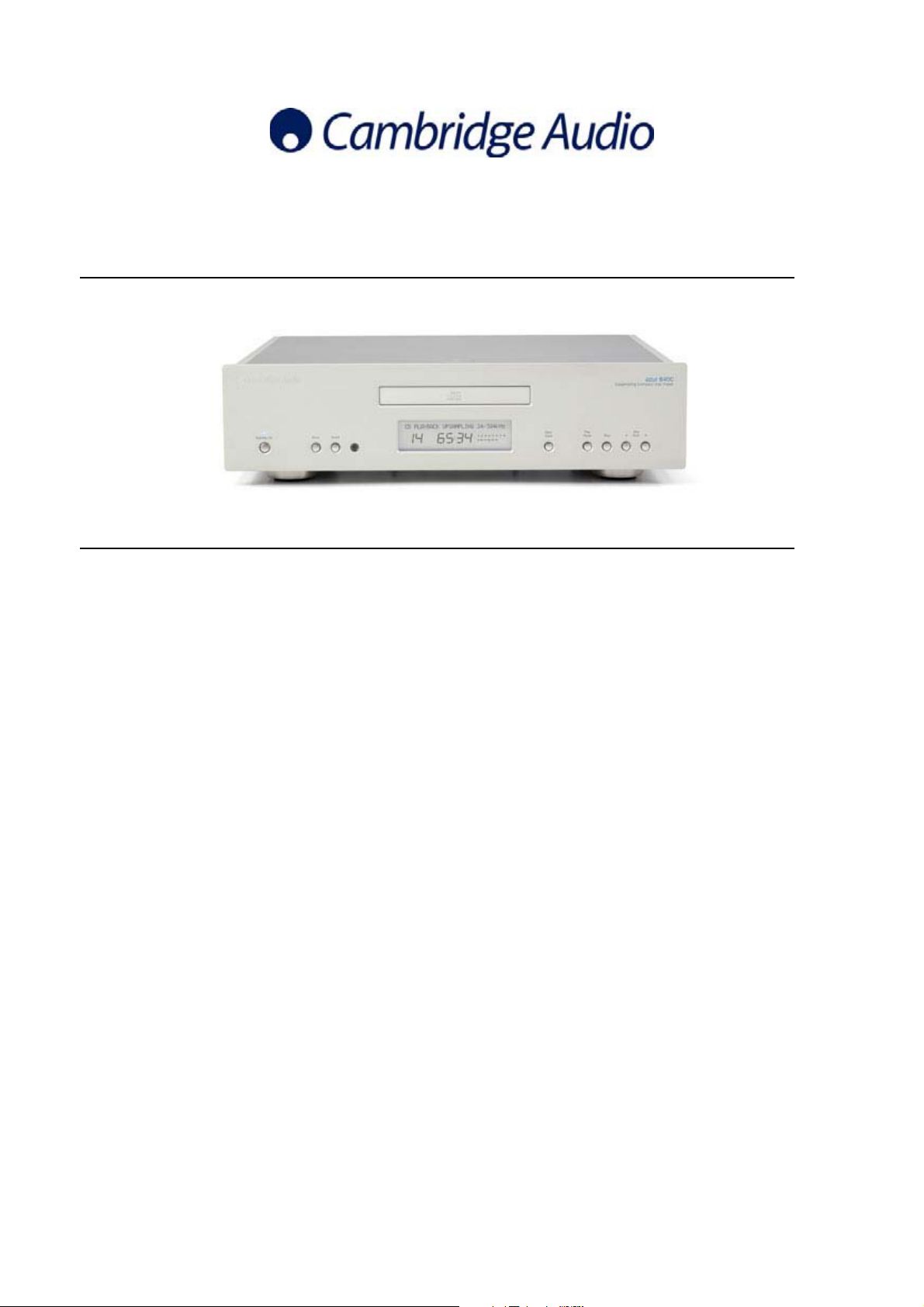
840C
Issue Date: 07thFebruary 2007
SERVICE MANUAL
SPECIFICATIONS:
D/A Converters Dual Analog Devices Total correlated jitter <130pS
Digital Filter Analog Devices Black Fin Crosstalk @20kHz < 114dB
Analog Filter 2 Pole Fully Differential
Frequency Response 20Hz 20kHz (+\ 0.1dB) Digital input sampling 32kHz, 44.1kHz,48kHz,88.2kHz
frequencies supported 96kHz, 176.4kHz, 192kHz
THD @ 1 KHz 0dBFs <0.0005%
THD @ 1Khz 10dBFs <0.0004%
THD @ 20 KHz 0dBFs <0.0007%
(4.5 x 16.9 x 14.7”)
IMD (19/20 kHz) 0dBFs <0.0002%
Linearity @ 90dBFs +/ 0.5dB
Stopband Rejection > 120dB
(>24 kHz)
AD1955 24 bit DAC’s
Crosstalk @1kHz < 130dB
ADSP BF532 32 bit DSP
Performing ATF™ Output impedance <50 ohms
Up sampling to 24 bit 384 kHz
Digital input word
widths supported 16 24 bit
Linear Phase Bessel Filter Digital output word
widths supported 16, 20, 24 bit
Digital output sampling 32 kHz 192 kHz pass through
frequencies supported (including 44.1 kHz for CD)
48 kHz, 96 kHz, 192 kHz up sampled
Audio output up sampling Fixed 24 bit, 384kHz
Dimensions (H x W x D) 115 x 430 x 360 mm
Weight 8.5kg (18.7lbs)
S to N ration, A weighted >113dB
Gallery Court Hankey Pl ace London SE1 4BB UK
Tel: +44 (0)20 7940 2200 Fax: +44 (0)20 7940 2233
AP21184/1
1

840C SERVICE MANUAL
TABLE OF CONTENTS
Safety Precautions & Important Notes 3
Laser Safety Precautions
Exploded Diagram
Exploded Diagram Parts List
Functional Block Diagram
Front Panel Circuit Diagram
Front Panel PCB Layout (Top Side)
Front Panel PCB Layout (Bottom Side)
Front Panel PCB BOM
Servo Circuit Diagram (DAC)
Servo Circuit Diagram (Servo)
Servo PCB Layout (Top Side)
Servo PCB Layout (Bottom Side)
Servo PCB BOM
Voltage Select Switch Circuit Diagram
Voltage Select Switch PCB Layout (Top Side)
Voltage Select Switch PCB Layout (Bottom Side)
Voltage Select Switch PCB BOM
4
5
6
7
8
9
10
11
12
13
14
15
16-17
18
19
20
21
DAC DSP Circuit Diagram (Abus)
DAC Test Signals (Main Signal Paths General)
DAC DSP Circuit Diagram (DSP)
DAC Test Signals (Main Signal Paths General)
DAC DSP Circuit Diagram (Filters)
DAC Test Signals (Main Signal Paths Left Channel)
DAC Test Signals (Main Signal Paths Right Channel)
DAC DSP Circuit Diagram (Supply)
DAC DSP Circuit Diagram (Flash)
DAC DSP Board Layout (Top Side)
DAC DSP Board Layout (Bottom Side)
DAC DSP PCB BOM
Mains PCB Circuit Diagram
Mains PCB Board Layout (Top Side)
Mains PCB Board Layout (Bottom Side)
Mains PCB BOM
IC Pin Layout Details
22
23
24
25
26
27-28
29-30
31
32
33
34
35-37
38
39
40
41
42-50
Circuit Description
Software Instructions
51
52-61
2
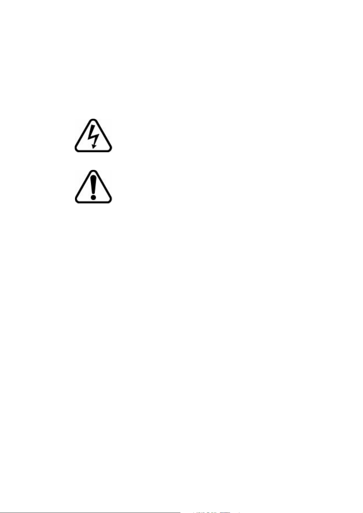
SAFETY PRECAUTIONS & IMPORTANT NOTES
1. Check that the rear of the product indicates the correct supply voltage for
your area.
2. The lighting flash with the arrowhead within an equilateral
triangle is intended to alert the user or service agent to the
presence of dangerous voltages within the product enclosure that
may be of sufficient magnitude to constitute a risk of electric shock
to persons.
3. The exclamation point within an equilateral triangle is intended
to alert the user or service agent to the presence of important
operating and maintenance (Servicing) instructions in the literature
accompanying the appliance.
4. This product complies with EEC Low Voltage (73/23/EEC) and
Electromagnetic Compatibility (89/336/EEC) Directives when used and serviced
in accordance with this manual. For continued compliance all components
marked safety and EMC critical must only be replaced by Cambridge Audio
approved parts.
5. Any unauthorised design alterations or additions will void the manufacturer’s
warranty; furthermore the manufacturer cannot accept responsibility for personal
injury or property damage resulting therefrom.
6. When servicing, care should be taken to observe the original routing and
dressing of the leads and it should be confirmed that they have been returned to
normal after re-assembly.
Notes on chip component replacement
Never reuse a component that has been removed from a PCB
Notice that the minus side of a tantalum capacitor may be damaged by heat
3
LASER SAFETY PRECAUTIONS
Caution: These labels may be attached to the unit on the rear and inside to
inform that it contains a laser component. Use of controls or adjustments, or
performance of procedures other than those specified within the service or
instruction manual may result in hazardous radiation exposure.
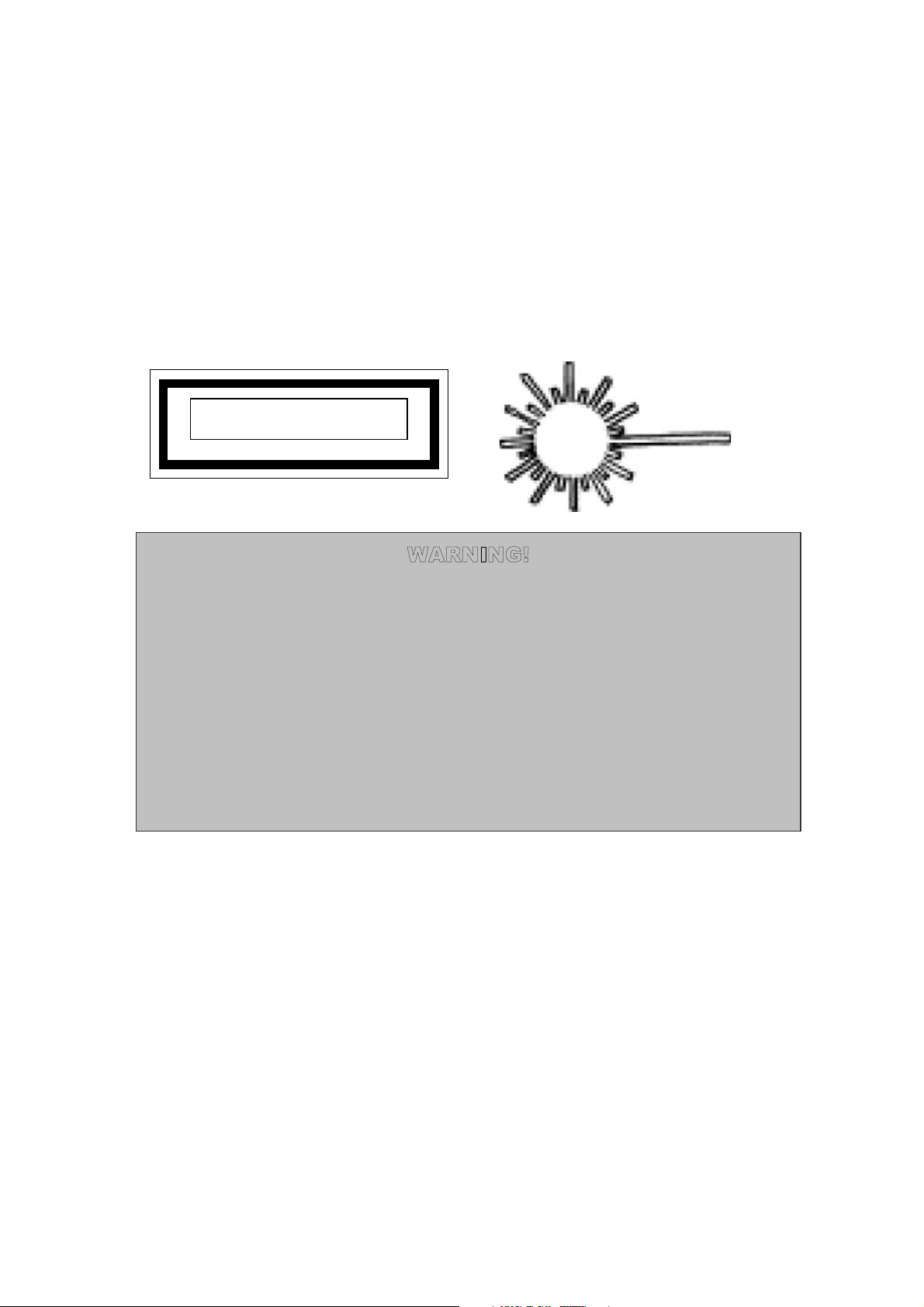
CLASS 1 LASER PRODUCT
WARNING!
1. Service should only be performed by qualified personnel.
2. This equipment has been designed and manufactured to meet
international safety standards; it is the legal responsibility of the repairer to
ensure that these safety standards are maintained.
3. Any repairs must be made in accordance with the relevant safety
standards.
4. It is essential that safety and EMC critical components are replaced with
Cambridge Azur approved parts only.
NOTES ON HANDLING THE OPTICAL PICK-UP BLOCK OR BASE UNIT
The laser diode in the optical pick-up block may suffer electrostatic breakdown because of the
potential difference generated by the charged electrostatic load, etc. on clothing and the human
body.
During repair, pay attention to electrostatic breakdown and also use the procedure in the printed
matter which is included in the repair parts.
The flexible board is easily damaged and should be handled with care.
NOTES ON LASER DIODE EMISSION CHECK
The laser beam on this model is concerated so as to be focused on the disc reflective surface by
the objective lens in the optical pick-up block. Therefore, when checking the laser diode
emission, observe from more than 30cm away from the objective lens.
4
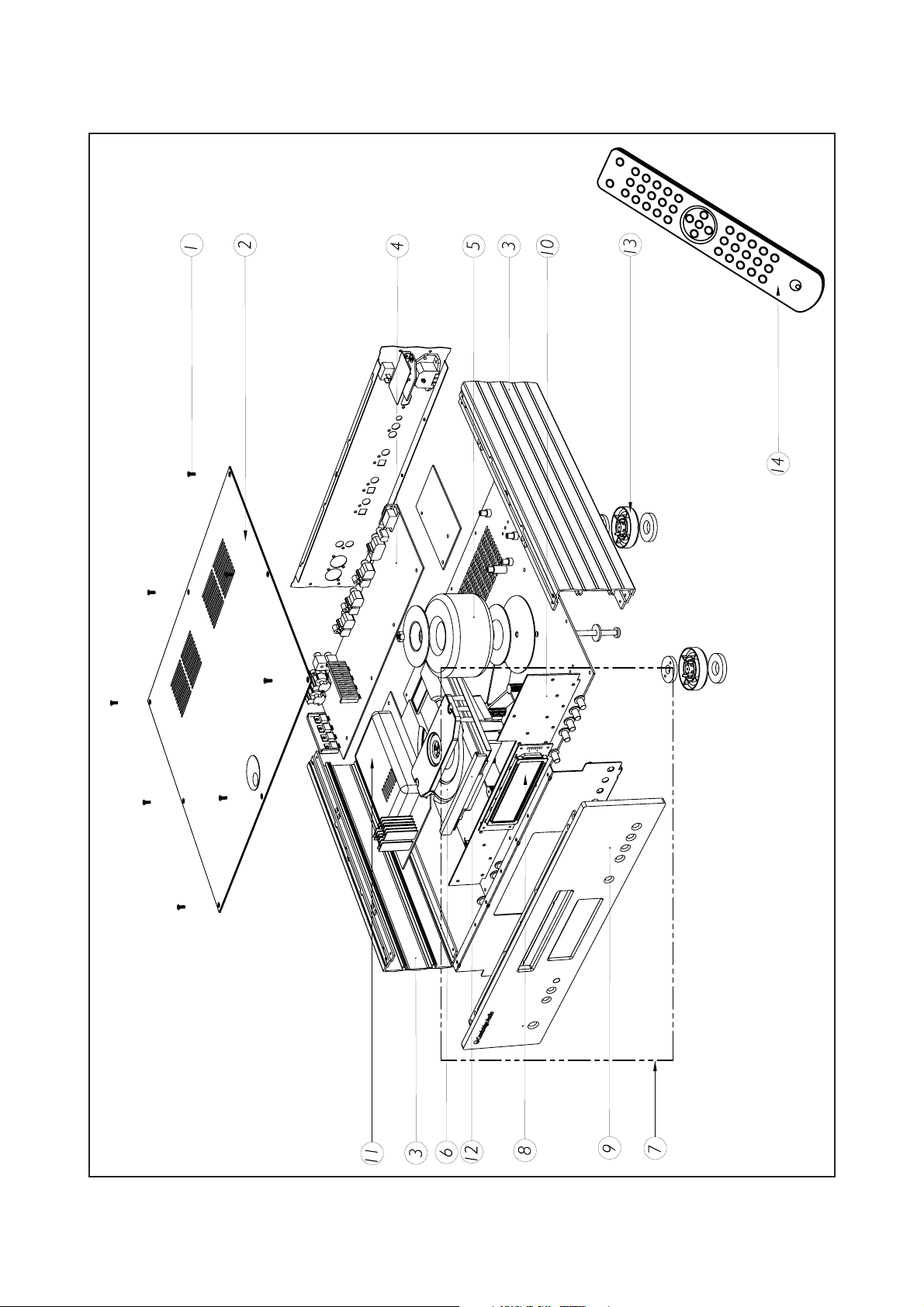
Cambridge Audio Azur 840C CD Player
Exploded Diagram
To enhance viewing, please print to A3 5
6
noitpircseDecnerefeRyrotcaFtraPPA.feRgniwarD
Azur V2 CD Mechan assy with Sanyo DA11V Rev A
Exploded Drawing Parts List
Cambridge Audio Azur 840C CD Player
1 PY1228 7003-008010E006 Screw M3*8 M/C 1/K Torx Recess ZN-PT (Silver)
1 PY1229 7003-008010E001 Screw M3*8 M/C 1/K Torx Recess BLK-PT (Black)
2 PY1218 6574-010003E000-01 Azur 840C Top Panel (Black)
2 PY1219 6574-010003E000-02 Azur 840C Top Panel (Silver)
3 PY1127 6574-150013E000-01 Azur 840A Side Panel, (Black)
3 PY1128 6574-150013E000A01 Azur 840A Side Panel, Silver
4 PY1110 4006-840058E001 840C DAC Module
5 PY1217 3200-080551E000 Transformer AC115/230V T08055A<AP19141/4>Azur-840C
6 PY940 9692-006002-201
V2 CD Sanyo Laser DA11V
7 PY1220 8584-001010E301 Azur 840C UK/EU Black Front Panel Assy
7 PY1221 8584-001000E301 Azur 840C UK/EU Silver Front Panel Assy
8 PY1222 4006-840001E000 Azur 840C Display Module MBCF00003B00V0 <RCL>
9 PY1223 6574-010002E000-01 Azur 840C Front Panel -B Artwork (Print Cool Grey 7C) Black
9 PY1224 6574-010002E000A01 Azur 840C Front Panel-S Artwork (Print Coll Grey 8C) Silver
10 PY1225 9484-001000E041 Azur-840C Control PCB Assy Rev A
Not Shown PY941 3009-110000-002
Exploded Diagram Parts List
11 PY1226 9484-001000E181 Azur-840C Servo PCBA <T-TYPE> Rev A
12 PY554 6564-010006-000-01 Azur 640C.B CD Door W/Silkscreen PMS Cool Grey 7C
12 PY568 6564-010006-000A01 Azur 640C.S CD Door W/Silkscreen PMS Cool Grey 7C
13 PY1122 6074-150004E000 Azur 840A Plastic Foot (Black) AP16837*
13 PY1124 6074-150004E000A01 Azur 840A Plastic Foot (Silver) AP16837*
14 PY1165 9805-084000E001 Azur 840A/C Remote Control Assy Rev A
Not Shown PY1227 5100-840100E100 Azur 840C Multilingual User Manual (AP18655*)
RS232
IR UNMOD
I/P
O/P
CN13
BALANCED O/P
UNBALANCED O/P
UNBALANCED O/P
CN12
CN14
BALANCED O/P
I/P IR MOD
FRONT PANEL PCB
U40
U50
U28
DIFFERENTIAL TOSINGLE ENDED
U39
LEFT CH
DC SERVOCIRCU TCURRENTSOURCE
U41U52Q7Q9
U38
CIRCUIT
DIFFERENTIAL FILTER/AMP
U37
ITOV
ITOV
DIFFERENTIAL TOSINGLE ENDED
U35
RIGHT CH
DC SERVOCIRCU TCURRENTSOURCE
U46U53Q 3Q5
U33
ITOV
CIRCUIT
DAC
U130
DAC1MCLK
DACCONTROL F
FLASHMEMORY
U32
FLASHADDRESS & DATA
U13
DSPCLK
Cambridge Audio Azur 840C CD Player
SPDF RX MCLK
DAC2MCLK
DAC1MCLK
DSPCLK
SPDF TX CLK
24.576MHz
CLOCK +BUFFER
X1 U15
MUTE
RESET
SPDF RX SET UP /F
U11
BTCLK
SDATAL
AUDIO DATALEFT
SPDIF RECEIVER
SPDF RX MCLK
SPDIF I/P SWITCHING
WDCLK
RESET
U131
DAC2MCLK
DACSET UP /F
DSP
RESET
SPDF TX SET UP /F
WDCLK
BTCLK
SDATAL
CBT
UBT
(SPDF SUBC ODE DATA)
(SPDF SUBC ODE DATA)
AUDIO DATAL&R
441/48/96/192 kHz
441 kHz FROM CD SERVO
U7
U12
SPDF TX CLK
SPDIF I/P SWITCHING
U9
TRANSMITTER
SPDIF
441 kHz PASS THRO SETT NG
DAC
U34
MUTE
DIFFERENTIAL FILTER/AMP
ITOV
RESET
48/96 192 kHz UP DOWN SAMPLED
U1 U2U3 Q1
FRONT PANEL IR MOD I/P IR MOD FROM REMOTE
U1
FRONTP ANNELBUTTONS
RS232 (LOGICLEVELS)
RL1 RL2RL3 Q 2 Q4 Q8
AUDIO O/P
MUTE CIRCU T
RELAY
WDCLK
BTCLK
SDATAL
OEI (PIC MUTE)
U19 U20
MODULATED R
(DOTMATR X)
MCRO TO LCD
MICROCONTROLER (PIC)
AUDIO DATALEFT
MCROCONTROLLER/DSP NTERFACE
BTCLK
WDCLK
SDATAL
(SPDF SUBC ODE DATA)
UBT
SPDIFI/P SWITCH NGCONTROL
AUDIO DATAL&R
U8
441 kHz FROM CD SERVO
441 kHz FROM CD SERVO
PASSTHRO SETT NG
DIG TAL POT
U3
BCPOVRESHCEM
(DOTMATR X)
MCRO TO LCD
LCD
KEYCOMMANDS TO SERVO (D G TAL POT FOR RES LADDER /P)
CDSERVO TO LCDCONNECT ONS
K1 K2I/P
DRAWER OPENCLOSE CONNECT ONS
CDSERVO TO MECH CONNECT ONS
DRAWER SPEED
2
U5U4U
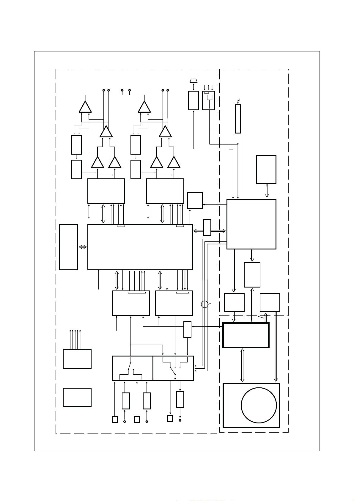
Functional Block Diagram
CONTROL
DRAWER OPENCLOSE CONNECT ONS
DAC PCB
PSU
LOGIC TO SPDIF
LEVEL
SPD F TO LOGIC
U23
OPTICAL
COAX
U4
CN3
SPDIF I/P1
LEVEL
SPD F TO LOGIC
U23
OPTICAL
COAX
U5
CN4
SPDIF I/P2
LEVEL
U6
OPTICAL
COAX
U10
CN5
SPDIF O/P
MECH AND SERVO PCB
To enhance viewing, please print to A3 7
+5V
GND
OPT
U1
CN7
SW2
Menu
SW1
Standby
D1
LED3MM BLUE
220R
R2
+5V
R9
220R
BC337
Q2
R13
10K
LED
Stop
SW4
SW3
SW8
SW6
Open/Cose
Seect
ForwardSk p
SW7
SW5
Pay/Pause
BackSk p
36
38
37
40
39
RB5
RB4
RB2
RB6 PGC
RB7 PGD
RB3 PGM
MCLR/VPP1RA0 AN0
RA2 AN2
RA1 AN1
RA3AN3/VREF5RA4/T0CK
U2
4
3
2
+5V
6
R6
10K
NT
CLK
SDTX
SDRX
CS
100nF
C9
+5V
10K
R19
R18
10K
LED
35
34
RB1
RB0/NT
RE0/RD AN5
RA5AN4/SS
7
8
R OUT
R N
SERAL TX
SERAL RX
SERVORESET
RESET
OE1#
MUTE
33
32
26
31
27
24
25
29
23
VSS
VDD
RC5/SDO
RD7/PSP730RD6/PSP6
RD5/PSP528RD4/PSP4
RC7 RX DT
RC6/TX/CK
RC4/SD/SDA
OSC1/CLKN13OSC2/CLKOUT
RC1/T1OS/CCP216RC2 CCP1
RE1/WR/AN6
VDD11VSS
RC3 SCK SCL
RCO/T1OSO/T1CK
RE2/CS/AN7
9
12
14
19
10
15
18
17
E
RS
SCL
D4
OSC1
OSC2
U7_S02
U9_S01
U7_SO1
100R
R32
RESET
SERVORESET
TO DAC BOARD CN9 (RS232/MUTE/SPDIF CNTRL)
D6D7SDA
22
21
RD3/PSP3
RD2/PSP2
RD1 PSP1
RD0 PSP0
PC16F874A
20
D5
JST2MM S8B -PH-KS
7
3
456
1
2
8
SO2 U7
SO1 U9
MUTE
SERAL RX
SO1 U7
SERAL TX
OE1
CONTROLB US
100R
100R
100R
100R
100R
R31
100R
10K
R12
R26
R29
R28
R30
R27
Q1
BC337
RMETAL 1/4W
220R
1/4WMe a F m
R37
RMETAL 1 4W
R36
220R
1/4WMeta F m
TSOP18 R RECE VER
3
2
1
C11
10U16V
C3
100n
R1
47R
+5V
RESET
+5V
10U16V
C13
100nF
C14
100R
100R
R25
R24
SP DATA RX
SP NT
SP DATA TX
SP CS
SP CLK
9
CN6
FN
GND12RN
VCC
OUT1
GND2
OUT27COM
U5
1
BA6218
3
5
6
8
9
100R
100R
100R
100R
R21
R22
R20
R23
LED
2345678
1
JST2MM S9B-PH KS
+5V
TO DAC BOARD CN8 (SPI)
Cambridge Audio Azur 840C CD Player
+8V
8
5
7
Vss
GP16GP2
+5V_SERVO
GP0
Vdd
MCLR4GP43CLKN
PC12C508
U4
1
2
D7
1N4004
1N4004
D6
680R
680R
R33
R34
123
4
5
CN9
DATA
MGND
C22
100nF
BZX79C5V1500MW
D3
BZX79C5V1500MW
D2
+8V
1N4004
C19
100nF
D4
10U16V
D5
1N4004
C18
MGND
2
1
CN8
MGND
345
DATA
COM2
COM1
COM3
COM4
LCD Connector 1
123
7
8
456
CN2
CONN-H8
LCD Connector 2
CN10
BRGHT
ON/OFF
C8
100nF
100R
R5
C7
10U16V
100nF
C4
D0D1
D2D3
D4D5
VssVdd
R/WE
VoRS
1
5
6
234
CN5
4a
6a
5a
1a2a3a
LCD
SEG10
SEG8
SEG67SEG5
SEG1
SEG9
SEG7
SEG45SEG34SEG2
SEG0
2
1
1
CN3
CONN-H8
SEG11
9
8
3
6
11
10
2
3
678
4
5
CN4
D6D7
7
7a
SEG12
13
12
1
+5V
LEDK
8
8a
LEDA
SEG13
15
14
234
X1
CRYSTAL
22pF
C5
C10
100nF
CONN 8HEAD DUALBOT
SEG1516SEG14
SEG1617SEG1718SEG1819COM120COM221COM322COM423NC
COM1
6
7
5
CONN H7
FREQ=20MHz
22pF
C6
BC337
Q3
+5V
LCD740C
24
COM3
COM4
COM2
R8
R11
13
R14
1K2
+5V_SERVO
ON OFF
13
14A16
H0
H11W1
U3
3
4
+5V_SERVO
1n50V X7R
C1
1234567
CN1
10OR
K1
K2
+5V
GND
REMOTE
ROUT
BRGHT
R35
100K
10K
R15
56R
R3
Q4
BC337
56R
R4
2
PREMULT 500R
R10
300R
RMETAL 1/8W
R17
4k7
1/8WMeta F m
RMETAL 1/8W
4k7
1/8WMe a F m
R16
5
9
7W012
10
L0
A0
A2
SCL
SDA
L1
GND
VCC
DS1803
8
16
C12
100nF
C2
1n50V X7R
100R
R7
CONN-H7
RESET
POWERDETECT
P5
SERVORESET
1
1
1
P2
PADEMC M3
P3
PADEMC M3
P4
PADEMC M3
C21
1nF
1nF
C20
C17
1nF
C16
1nF
C15
1nF
1
1
P1
PADEMC M3
PADEMC M3
AP19135/4 Front Panel Circuit Diagram
FROMSERVO BOARD DRAWER OPEN/CLOSE (SP )
TOMECH DRAWER OPEN/CLOSE (SP )
From Servo Board (LCD)
To Servo Board
To enhance viewing, please print to A3 8
Cambridge Audio Azur 840C CD Player
AP19135/3 Front Panel Board Layout (Top Side)
To enhance viewing, please print to A3 9
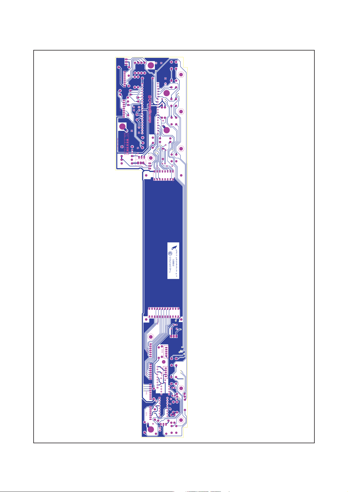
Cambridge Audio Azur 840C CD Player
AP19135/3 Front Panel Board Layout (Bottom Side)
To enhance viewing, please print to A3 10
m
m
m
2
m
0
7
m
m
0
m
m
m
9
m
0
0
t
8
0
Cambridge Audio Azur 840C Front Panel PCB BOM
AP Part
No.
RESISTORS
47R 0.25 W 1% Metal Fil
56R 0.25 W 1% Metal Fil
100R 0.25 W 1% Metal Fil
220R 0.25 W 1% Metal Fil
300R 0.25 W 1% Metal Fil
680R 0.125 W 1% Metal Fil
1K2 0.25 W 1% Metal Fil
4K7 0.25 W 1% Metal Fil
10k 0.25 W 1% Metal Fil
100K 0.25 W 1% Metal Fil
PRE MULTI 500R
CAPACITORS
22p 6C,5C2mm0.5=hctiP,OPNcimareCF
10uF
SEMICONDUCTORS
PY983 DS18030-05
PY260 BA621
Value Description Factory Part No Qty Component Ident Notes
Side adjust Footprint 9.5 x 4.5
mm
Miniature 16V Pitch 2.5mm
Hei
ght 5.2mm
DIGITAL PO T 4118-030051E20
1012-201014E00
1016-801016E02
VR B500 OHM +10% WI
3296NOXOX-XA1013
1R1
2 R3, R4
16 R5, R7, R8, R20-R3
4 R2, R9, R36, R3
1 R10
2 R33, R34
1 R14
2 R16, R1 7
6 R6, R12, R13, R15,R18, R1
1 R35
1 R11
C3, C4, C8-C10, C12, C14,
9mm0.5=hctiPV05cimareCFn001
C19, C22
4 C7, C11, C13, C18
1U1REVIECERRIPOSTV3SS6381POST
2U1CIPP/I-A778F61CIP
1U3
4U1CIPP/I-A805C21CIP
5U1CIREVIRDDC
AP19138/5
Mount on bottom side of PCB with
screw adjust facing upwards
12C,02C,71C-51C,2C,1C7mm0.5=hctiPV05cimareCFn1
Mount 13.5mm height from PCB, Please
support using foam pad spacer
Programme with AP20058/2, Please add
version label - See AP Service Dept.
Programme with AP20231/1, Please add
version label - See AP Service Dep
TRANSISTORS
PY214 BC33 7 NPN SMALL SIGNA L 4 Q1-Q4
DIODES
1D1EULBDEL
5V1 ZENE R BZX79C5V1 1402-511201E20
MISCELLANEOUS
PY043 TACT SWITCH
TACT SW 2P2T KPT-1105A
(5MM)
2 D2, D3
8 SW1-SW8
7D,6D,5D,4D4REIFITCERESOPRUPLARENEG4004N1
MPP03-+1X1SU94-CHFP02LCMM5.3TUOBATHGIEH,zHM02LATSYRCzHM02
Note: resistors, capacitors and other 'generic' electronic components are
not usually stocked by the manufacturer. Please obtain these locally.
11
RL1:A
1
R83
120R 0.5W
2
Q4
D7
N4004
Q3
8050
Q5
9012
8050
R84
4K7
AC
N4004
D6
C63
4.7uF16V
R86
3K9
560R
R85
9012
Q6
100R
R87
C55
47uF 16V
R68
100R
N4148
D1
R89
330k
R88
1K
R90
390R
145V
47K
R81
10pF
C36
+8V
C43
10uF25V
1
U4A
84
3
2
12K
R80
NJM2100
LCH
RCH
LCH
RCH
GND
CN9
1
2
3
3
RL1B
5
4
R70
56K
C35
01uF
20K
R79
20K
R72
C38
390pF
GND
CN10
3
1
2
6
RL1C
7
8
R69
100R
R71
56K
C34
10uF25V
7
U4:B
NJM2100
6
C37
220uF16V
5
12K
R74
MUTE
GND
ROUT
LOUT
MUTE1
CN11
12345
47K
R73
10pF
C33
GND
Cambridge Audio Azur 840C CD Player
+5V
D12
1N4001
15K
R82
C39
10uF25V
C40
10uF25V
C41
0.1uF
8
7
6
5
VA+
AGND
AOUTL
AOUTR
U5
SDATA
LRCK3MCLK
DEM SCL
CS4333/38
2
1
4
123
4
5
D G DATA
CN13
390pF
C42
15K
R75
C32
10uF25V
C88
1nF
1
2
CN14
MCLK
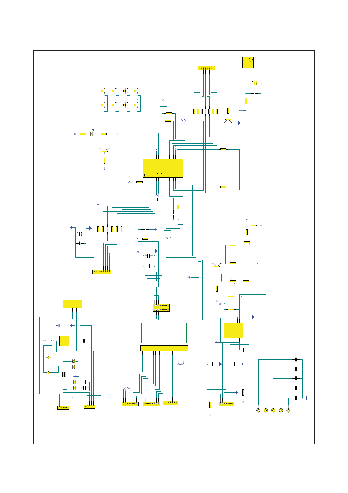
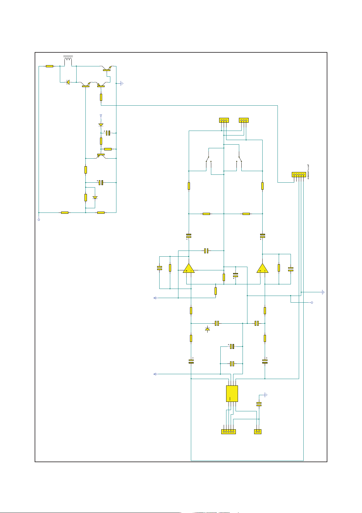
AP18432/3 CD Servo PCB Schematic (DAC)
To enhance viewing, please print to A3 12
SLT+
FM+
SLT
FMDMDM+
CN15
2
3
1
4
5
6
MOTORDR VE
C58
100nF
C57
70uF16V
C 6
+5V
C45
3
100nF
VO
GND
2
V
U8
78 5
1
C44
100nF
+8V
C47
470uF16V
1 0nF
C48
3
VO
GND
2
V
808
U7
1
CN21
FPD S
1
2
C51
R31
10K
+5V
R30
10K
+8V
PWRDET
RESET
GND
K1
REMOTE
+5V
K2
CN7
567
4
123
CONTROLKE S
C50
3300uF25V
100nF
C49
FU1
T2AL
100nF
C54
C52
145V
N4004
100nF
N4 04
N4 04
D4
D3
N4004
1 0nF
C53
D2
D5
100 F
2
1
AC N
CN19
R67
14mm nk 840c n y
AC
GND
OPEN
CLOSE
OLT
CLT
CN8
1
234
5
D AW DR E
+5V+5V
R29
10K
R34
470R
8550
Q 0
Q9
8550
70R
R 3
Q11
8050
8050
Q 2
Q7
80 0
Q8
8050
+5V
R64
D10
R 8
10K
10K
1N4148
D11
1N4148
100nF
3
15
18
19
24
14
17
20
22
16
21
23
V 4
V 3
S CC
SGND
PVC 3
PVC 4
OUT 3
OUT 4
PWGND
PWGND
OUT+ 3
OUT+ 4
C56
VN
PVCC
PWGND
OUT+
VR
OUT
U6
6
2
1
3
4
5
+8V
100nF
C59
470pF
C24
CN20
1
220uF16V
VN2
PVC 2
PWGND
VC
OUT+ 2
OUT 2
TA209 N
2
7
9
8
11
10
C61
1 0nF
C60
0047uF
3K3
470pF
C25
R44
ROUT
MUTE1
MUTE
CN12
MUTE
2
234
5
Cambridge Audio Azur 840C CD Player
NOF T FOR 740 840C
R24 10K
R23 10K
4K7
R32
R25 1K
R26 10K
L3
REMOTE
+5V
1
123
456
7
23456
CD
CN5
CN6
SEG18
SEG16
SEG11
SEG17
SEG15
SEG14
SEG13
SEG12
SEG10
SEG9
SEG8
SEG7
SEG6
100uH
NC
NC
44
41
50
49
48
46
43NC42
40LT39
38
37
36
33
45
1 0nF
C86
V S
OOT
ADK47ADK2
ADK3
VA EF
51
+5VDD
VDD
52
L/L
53
NC
NC
54
NC
NC
R27
55
10K
NC
NC
56
NC
NC
57
NC
NC
58
NC
NC
LK1
LNK
59
NC
NC
60
OPEN= F/L
SHORT= /L
NC
NC
61
NC
NC
62
NC
NC
63
NC
NC
64
NC
NC
65
NC
NC
66
NC
NC
67
NC
NC
68
NC
NC
69
NC
NC
70
NC
NC
71
NC
NC
72
NC
NC
73
SEG8
74
SEG7
75
SEG6
76
SEG5
77
SEG4
78
SEG3
79
SEG2
80
SEG1
S G9
S G 0
S G883S G784S G685S G586S G4
81
82
8
7
12345
678
R22NCR21
+5V
CD
CD
CN4
SEG5
SEG3
SEG2
SEG0
COM0
COM3
SEG4
SEG1
COM1
COM2
32EE31
34
NC
CLT
OLT
B S3
B S235B S
B S0
BUCK
DOP N
DC OSE
PWRDET
U3
TOSHCDMCU
S G3
S G0
COM2
S G289S G
COM3
87
88
90
91
92
93
22K
SETLCDCONTRA T
30
RS
29
CORW
28
NC
NC
27
NC
NC
26
NC
NC
25
NC
NC
24
NC
NC
23
NC
NC
10K
2K2
22
NC
NC
21
NC
NC
R66
R17
20
NC
NC
19
NC
NC
18
NC
NC
+5V
17
WAT)
16
SO2)
15
S2)
14
SC 2
13
NC
NC
12
NC
NC
11
NC
NC
10
MUTE
9
RM O E
8
NC
NC
7
TST
6
NC
NC
5
REMOTE
NC
NC
4
3
XN
2
XOUT
1
VSS
COM0
V C96NC
NC
COM
VDD
94
99
95
97NC98
100
NC
NC
NC
100uF16V
C85
100uH
C83
470uF16V
L4
+5VCC
C80
25pF
5pF
C81
CRYSTAL
X2
73728MHz
+5V
C84
220uF16V
00uH
5
FCTRTR+
FC+
PDVRLD
F
C
GND
BAD
VC
E
CN16
14
15
16
L2
10uH
Q1
90 5
100 F 6V
R62
C62
100nF
15R
C 9
R59
60
K
C21
00047uF
27K
R61
C22 0047uF
C23
0 47uF
C70
3K3473K3
46
R45
3K3
0K
43
R42
3K3
41
3K3
0047uF
0047uF
C27
C26
GND
LOUT
1
OSC
GND
GND
CN17
XTAL
CN18
XTALO
1
1
2
2
4 uF 6V
C18 47uF16V
C19
0 47uF
C87
1nF
C15
0047uF
10R1 4W
15pF
15pF
X1
R 0
CRY TAL
C17
C16
6 344MHz
R36
R35
+5V
R65
10K
C79
1 0nF
Q13
901 C
10K
R18
4K7
R76
R19
3K3
D9
1N4148
10uF16V
C82
1K
R20
+5VDD
1
8
23456
7
CN3
5V
S2
PROGRAMMNG
GND
SO2
SCK2
BOOT
WAT
RESET
VCC
2
11
13
0R
R58
82K
U1
100nF
C4
MECH
6
2
345
8
9
1
7
10
56K
47K
47K
56K
47K
47K
R50
R48
R51
R49
R 2
R 7
00nF
C64
C67
1 0nF
7uF16V
C 0
C65
220uF 6V
C66
0047uF
0
1
2
4FP5
8
13
9
15
6
11
14
3
12
7
EO
EN
SEL
TN
T B
MD
LDO
S AD
2 RO
RFRP0BTC
SEB
RFCT2PKC
FEO
FEN
VRO
RFRPN
6
9
8
3
4
7
2
0 2uF
0 2uF
C72
C3
100nF
C71
50
49
48
U2
TRO
FOO
V EF
51
RFGC
52
EBC0
53
EBC1
54
NC
EBC2
55
DMO
56
2V EF
57
SL
58
NC
LGA
59
NC
LGB
60
NC
FLGC
61
NC
FLGD
62
VDD3
63
VS3
64
NC
O0
65
NC
O1
66
NC
O2
67
NC
O3
68
NC
DMOUT
69
NC
KSE
70
NC
DACT
71
TEIN
72
TESO1
73
VS4
74
P I
75
NC
PXO
76
VDD4
77
X SS
78
I
79
XO
80
XVDD
DV R
DVDD
83
81RO82
38
C28 47uF16V
C14 22uF16V
R39
10K
L1
TP
RFGO
6
5
C78
46
47
TEZ
47uH
CC
FN
R GC
GMAD
GND
RFO
RFN2
AGCN
GVSW
TA2153 N
8
7
9
0
100 F
C2
220R
R63
R4
3pF
C1
10K
R2
R1
C73
1K
100pF
R3
C7
001u
47uF16V
0047uF
C5
C77
47uF16V
43
36
40
37
34
33
44
38
35
45
42
41
39
FE
RF
TE
FCT
BAD
RFZ
LCO
COF
TSN
R RP
AVSS
A DD
VC REF
TC94 2F
DV L86T ST87T ST288T ST389BU 0
BU 292BU 393VDD94VSS95BUCK96CCE97T ST4
DVR
BUS
84LO85
98
90
91
NCNCNC
37
R11 10K
R12 10K
R13 10K
R14 10K
R15 10K
J1
100R
68
2uF
10K
10K
10K
10K
56
55
54
53
100K
2K2
C6 00 27uF
C75 00 uF
C74 47uF16V
C76
47pF
C8
31
32
0015uF
PFO
L FN
PV EF
TMAX
TMAXS
PDO
ZD T
HSW
P VREF
TS O0
VDD2
MONT
COS
S DA
S CK
S SY
SSY
DATA
V S2
VDD1
CCK
S OK
PF
MBOV
9
DOUT
8
AOUT
7
B K
6
V S1
5
L CK
4
EMPH
3
2
HSO
1
TST0
RST
T M D
99
100
NC
NC
0047uF
1uF16V
C12
C13
R8 10K
R7 68K
R9 7K
R5 5K
R6
30
29
28
27
26
NC
25
24
23
22
NC
21
NC
20
NC
18
NC
18
NC
17
NC
16
NC
15
14
13
NC
12
NC
11
NC
10
NC
NC
NC
NC
47uF16V
C29
R16
10K
C9
220K
D8
47uF16V
C10
47uF16V
C11
0047uF
47R
R10
+5V
123
CN1
DG TAL OUT
+5V
GND
DOUT
4
5
123
CN2
DATAOUT
BCK
GND
EMPH
PCMD
LRCK
1N41 8
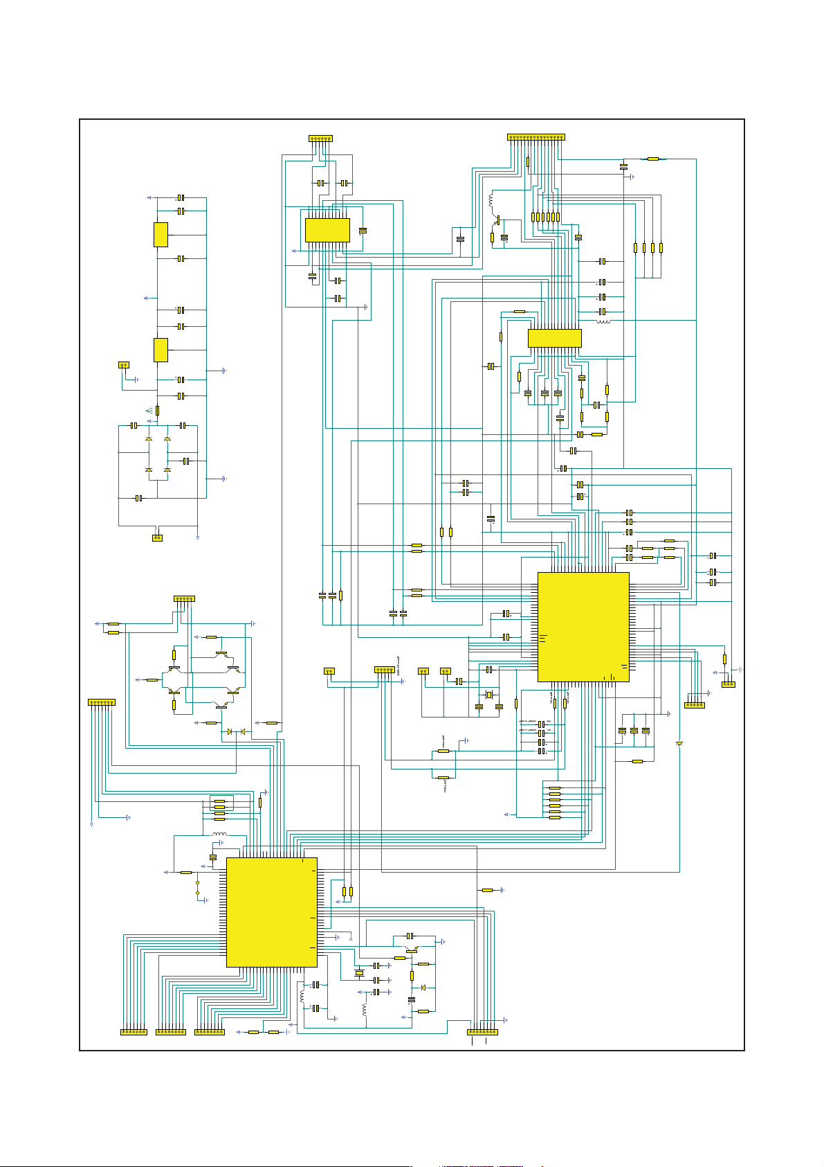
AP18432/3 CD Servo PCB Schematic (Servo)
To enhance viewing, please print to A3 13
Cambridge Audio Azur 840C CD Player
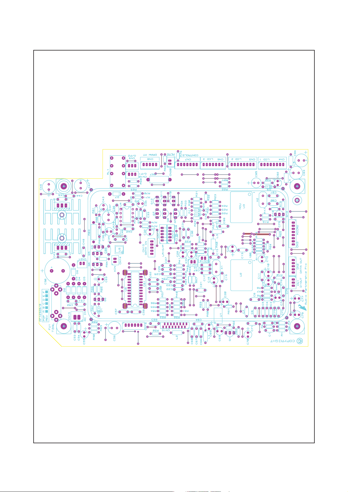
AP12927/8 CD Servo Board Layout (Top Side)
To enhance viewing, please print to A3 14
Cambridge Audio Azur 840C CD Player
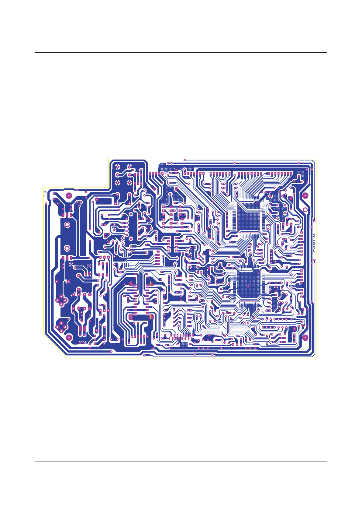
AP12927/8 CD Servo Board Layout (Bottom Side)
To enhance viewing, please print to A3 15
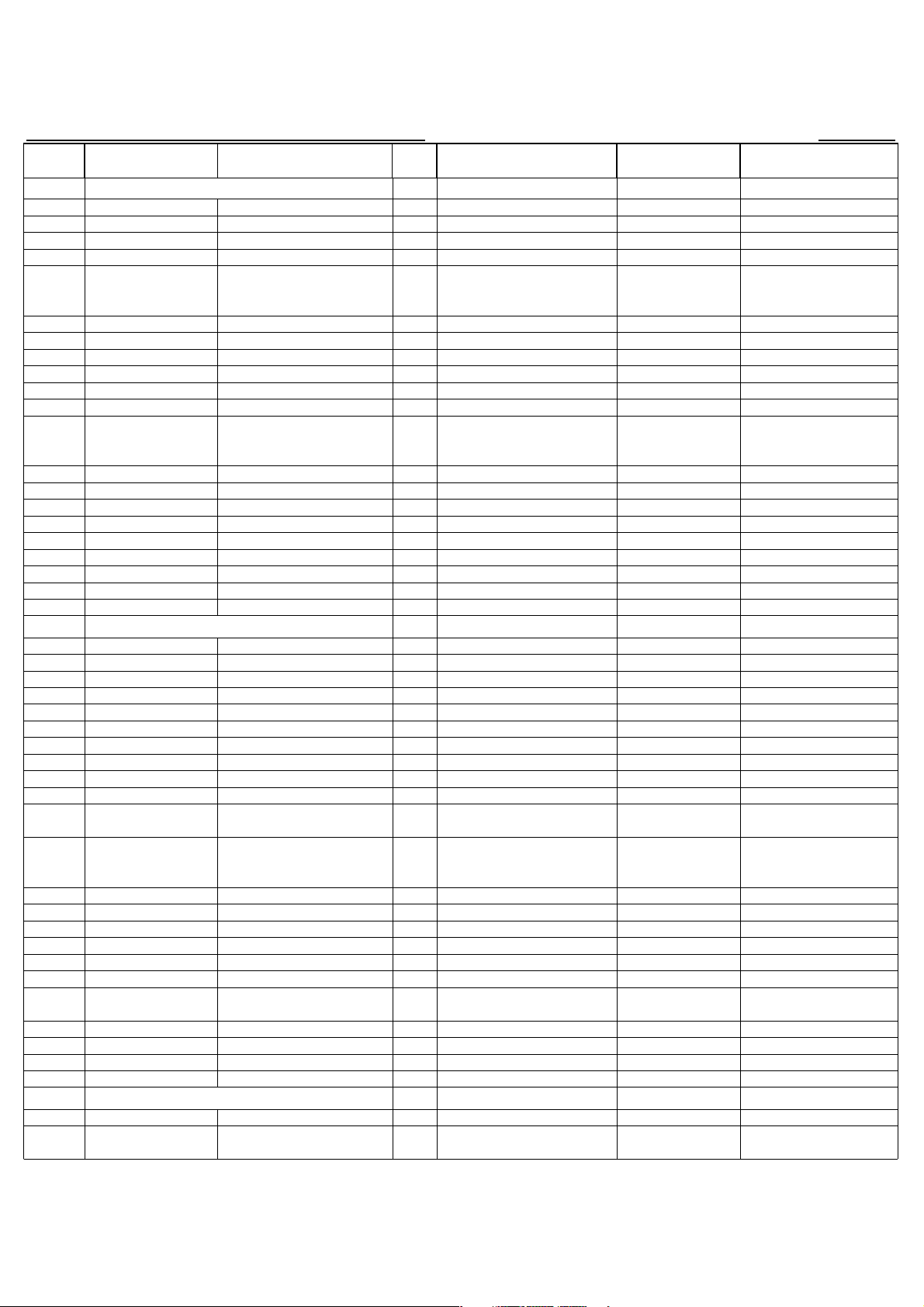
Cambridge Audio Azur 840C Servo PCB Assembly BOM
AP Part
No
RESISTORS
15R 0.125 W Metal Film Resistor 1 R62
100R
1K
3K3 0.125 W Metal Film Resistor 7 R19, 41, 42, 44, 45, 46, 47 1013-302018-000
10K
22K 0.125 W Metal Film Resistor 1 R21
27K 0.125 W Metal Film Resistor 1 R61
47K 0.125 W Metal Film Resistor 5 R9, 48, 49, 50, 51 1014-703016-000
56K 0.125 W Metal Film Resistor 2 R52, 57
82K
100K 0.125 W Metal Film Resistor 1 R63 1011-004016-000
220K 0.125 W Metal Film Resistor 1 R6 1012-204016-000
CAPACITORS
3pF Ceramic COG 50V 5mm Pitch 1 C1
15pF Ceramic COG 50V 5mm Pitch 2 C16, 17 1100-150043-000
25pF Ceramic COG 50V 5mm Pitch 2 C80, 81 1100-250042-000
47pF Ceramic COG 50V 5mm Pitch 1 C76 1100-470043-000
100pF Ceramic COG 50V 5mm Pitch 1 C73
470pF Ceramic 50V 5mm Pitch 2 C24, 25 1100-471043-000
10nF Ceramic 50V 5mm Pitch 1 C75 1100-103043-000
10nF Mylar 5mm Pitch 1 C7
15nF Ceramic 50V 5mm Pitch 1 C8 1100-153043-000
47nF Ceramic 50V 5mm Pitch 11
100nF Ceramic 50V 5mm Pitch 20
220nF Ceramic 50V 5mm Pitch 2 C3, 72 1100-224044-000
1uF
10uF 16V Electrolytic 1 C82 1102-100024-000
22uF 16V Electrolytic 2 C14, 68 1102-220014-000
47uF 16V Electrolytic 10
100uF 16V Electrolytic 2 C69, 85 1102-101014-000
220uF 16V Electrolytic 3 C56, 65, 84 1102-221014-000
470uF 16V Electrolytic 3 C46, 47, 83 1102-471014-000
3300uF 25V Electrolytic 1 C50 1102-332024-000
SEMICONDUCTORS
PY474 TA2153FN TOSHIBA RF Amplier 1 U1 4121-530103-000
PY475 TC9462FG
Value Description Qty Component Ident Factory Part no Notes
0.125 W Metal Film Resistor 1 wirelink ( J1 ) 1011-001016-000
0.125 W Metal Film Resistor 5 R3, 20, 25, 60 1011-002018-000
R2, 8, 11, 12, 13, 14, 15, 16, 17,
0.125 W Metal Film Resistor 26
0.125 W Metal Film Resistor 1 R59 1018-203018-000
16V Electrolytic 1 C12 1102-107044-000
TOSHIBA Digital Servo-chip
Processor
18, 26, 27, 28, 29, 30, 31, 39, 43,
53, 54, 55, 56, 64, 65
C5, 11, 13, 15, 19, 22, 23, 26, 27,
60, 66
C2, 4, 44, 45, 48, 49, 51, 52, 53,
54, 57, 58, 59, 61, 62, 64, 67, 71,
79, 86
C9, 10, 18, 20, 28, 29, 70, 74, 77,
78
1011-003016-000
1100-473044-000
1106-104044-000
1102-470014-000
AP19969/3
000-410000-110104R1rotsiseRmliFlateMW52.0R01
knilesU.YLNOC048roF76R1knilmm41knil
000-810007-4101,01R1rotsiseRmliFlateMW521.0R74
wirelink is positioned
between C68 and L2. This
must be 100R resistor
000-810102-21014R1rotsiseRmliFlateMW521.0R022
000-610107-410143,33R2rotsiseRmliFlateMW521.0R074
000-610202-210166,1R2rotsiseRmliFlateMW521.02K2
000-610207-410167,23R2rotsiseRmliFlateMW521.07K4
000-810305-1101,5R1rotsiseRmliFlateMW521.0K51
000-810308-6101,7R2rotsiseRmliFlateMW521.0K86
000-340201-001178C1hctiPmm5V05cimareCFn1
000-360272-10116C1hctiPmm5ralyM7n2
000-260274-101112C1hctiPmm5ralyM7n4
ABIHSOTPFQSNIP001000-321026-49142U1
Note: resistors, capacitors and other 'generic' electronic components are
not usually stocked by the manufacturer. Please obtain these locally.
16
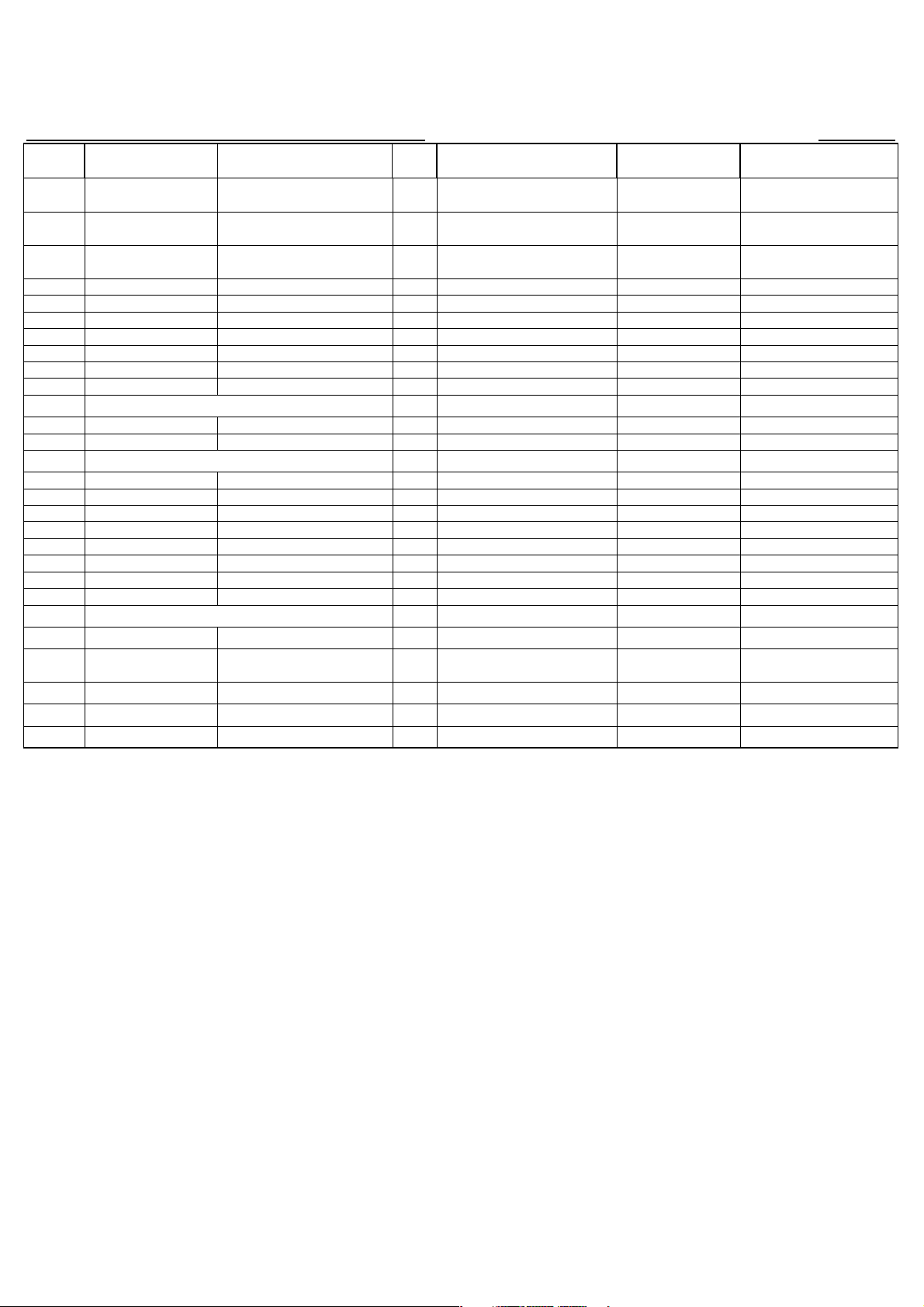
Cambridge Audio Azur 840C Servo PCB Assembly BOM
AP Part
No
PY565 TOSHCDMCU
PY014
PY558 9014C NPN Transistor 1 Q13 1300-901400-100
C8050D NPN Transistor TO92 4 Q7, 8, 11, 12 1300-805000-100
1N4148
1N4004 Rectier Diode 4 D2, 3, 4, 5 1401-140040-000 stand up o PCB by 7.5mm
CRYSTALS
CONNECTORS
MISCELLANEOUS
T2AL
10uH
Value Description Qty Component Ident Factory Part no Notes
MCU TMP87EP26F-1J15 SOP
TOSHIBA
Signal Diode 3 D9, 10, 11 1401-141480-000
2A delay 20mm Fuse 250V LBC
(low breaking capacity)
Inductor 8mm Pitch 1 L2
000-301062-78143U1
t heatsink to top of driver
000-350029-02146U1CIrevirdrewoPABIHSOTN2902AT374YP
IC
mount on heatsing using
006-203080-87147U1rotalugeRV8+022-OT8087613YP
heatsink comound only
007-433050-87148U1rotalugeRV5+022-OT5087530DP
001-000558-103101,9Q2rotsisnarTPNP0558C955YP
001-005109-10311Q1rotsisnarTPNPC5109065YP
000-343961-00611X1hctiPmm5niP2zHM4439.61720YP
099-282737-00612X1hctiPmm5niP2zHM8273.7165YP
100-000200-00321271NC2TSJhctiPmm2yaW2
100-000300-0032,1NC1TSJhctiPmm2yaW3
000-000500-0032,8,2NC2TSJhctiPmm2yaW5
000-000600-003251NC1TSJhctiPmm2yaW6
000-000700-00327,6NC2TSJhctiPmm2yaW7
000-000800-00325,4,3NC3TSJhctiPmm2yaW8
300-001200-003291NC1TSJhctiPmm5.2yaW2
000-109610-103261NC1hctiPmm0.1CFFyaW61
100-001050-13041UF1redloHesuFtnuoMBCPmm02
100-200816-03041UF1
001-003074-40511L1hctiPmm8rotcudnIHu74
001-003101-40515,4,3L3hctiPmm8rotcudnIHu001
AP19969/3
Note: resistors, capacitors and other 'generic' electronic components are
not usually stocked by the manufacturer. Please obtain these locally.
17
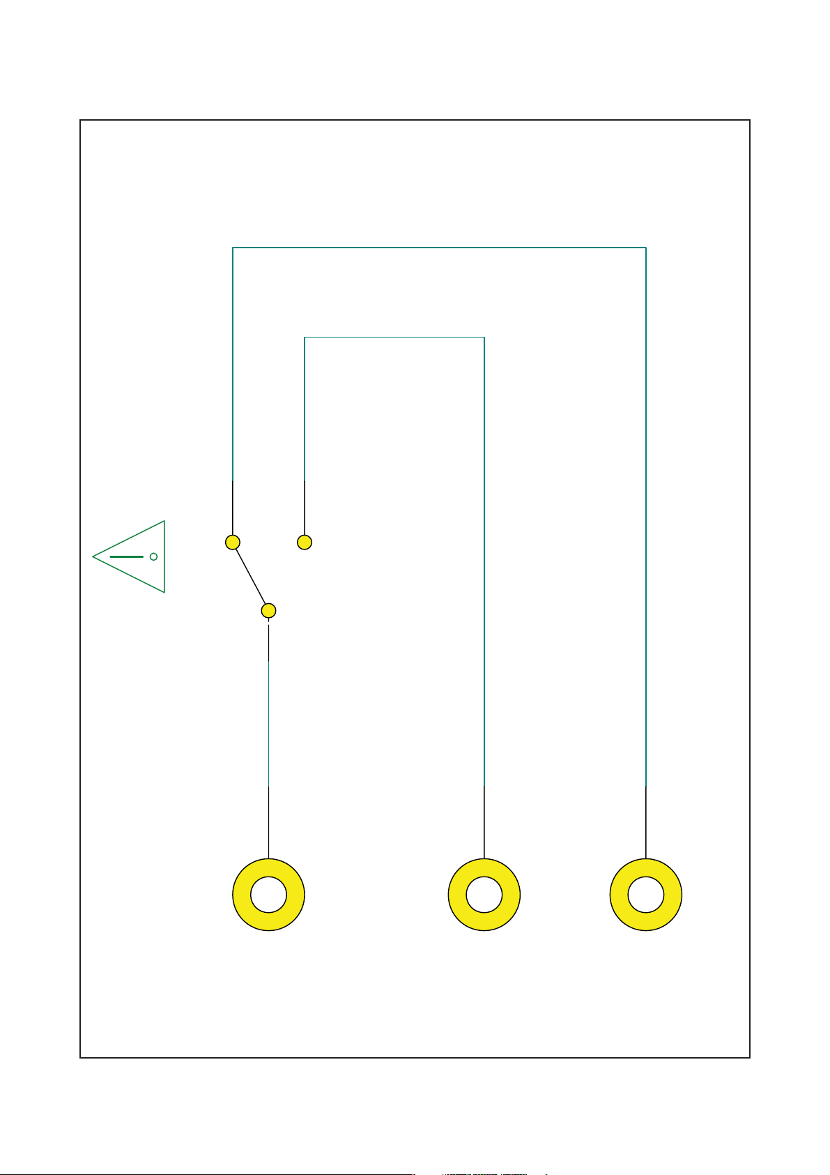
VOLTSELECT RF1002B
SW1
Cambridge Audio Azur 840C CD Player
115/230V Marking
AP17977/2 Voltage Select Switch PCB Schematic
J2
FROM J4 (Common)
J1
BROWN (230V)
J3
BLACK (115V)
To enhance viewing, please print to A3 18
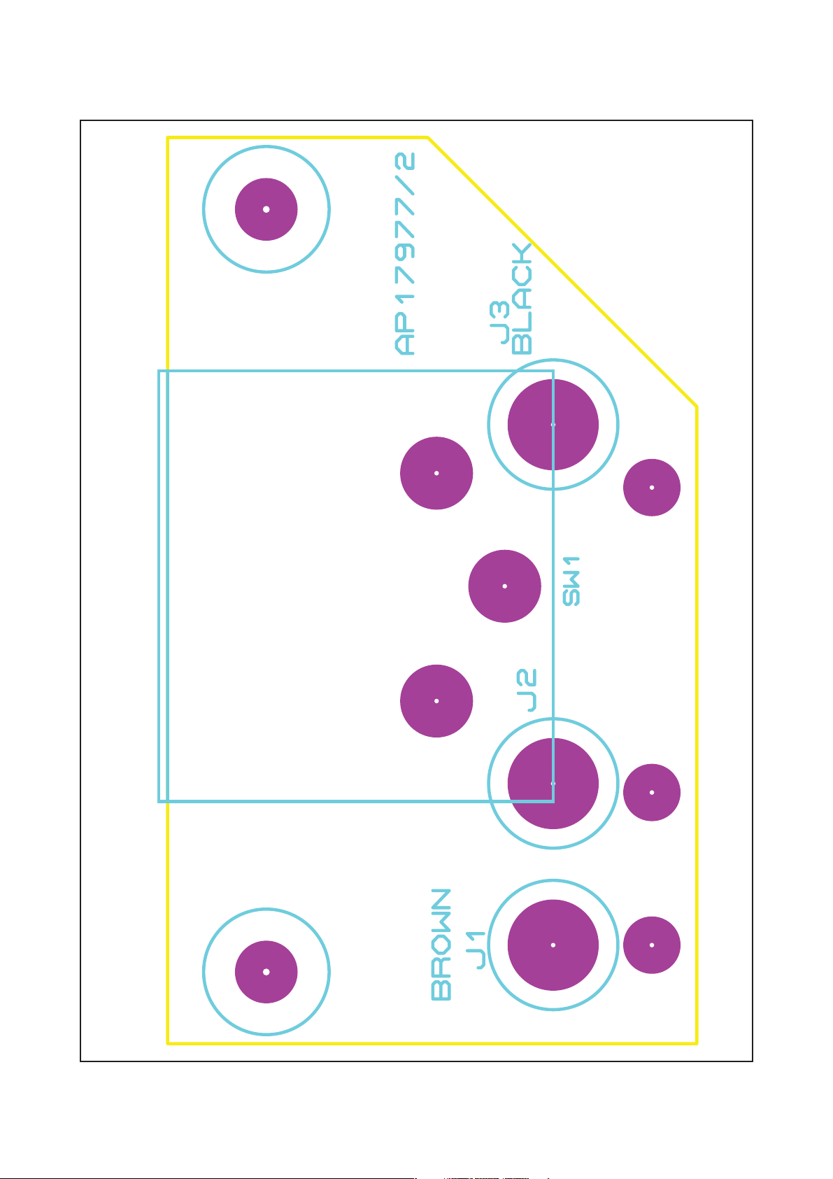
Cambridge Audio Azur 840C CD Player
AP17977/2 Voltage Select Switch Board Layout (Top Side)
To enhance viewing, please print to A3 19
 Loading...