


Burr Brown PCM1702P, PCM1702P-J, PCM1702P-K, PCM1702U, PCM1702U-J Datasheet
...
|
|
® |
PCM1702P |
|||
|
||||||
|
|
|
|
|
|
|
|
|
|
|
|
|
PCM1702U |
|
|
|
|
|
|
|
BiCMOS Advanced Sign Magnitude 20-Bit
DIGITAL-TO-ANALOG CONVERTER
FEATURES
●ULTRA LOW –96dB max THD+N (No External Adjustment Required)
●NEAR-IDEAL LOW LEVEL OPERATION
●GLITCH-FREE OUTPUT
●120dB SNR TYP (A-Weight Method)
●INDUSTRY STD SERIAL INPUT FORMAT
●FAST (200ns) CURRENT OUTPUT (±1.2mA)
●CAPABLE OF 16X OVERSAMPLING
●COMPLETE WITH REFERENCE
●LOW POWER (150mW typ)
DESCRIPTION
The PCM1702 is a precision 20-bit digital-to-analog converter with ultra-low distortion (–96dB typ with a full scale output). Incorporated into the PCM1702 is an advanced sign magnitude architecture that eliminates unwanted glitches and other nonlinearities around bipolar zero. The PCM1702 also features a very low noise (120dB typ SNR: A-weighted method) and fast settling current output (200ns typ, 1.2mA step) which is capable of 16X oversampling rates.
Applications include very low distortion frequency synthesis and high-end consumer and professional digital audio applications.
Clock |
Input Shift Register |
Balanced Current |
|
Data |
and Control Logic |
Segment DAC A |
|
LE |
|
|
|
DCOM |
|
Balanced Current |
IOUT |
ACOM |
|
||
|
Segment DAC B |
||
+VCC |
Reference |
|
|
|
|
||
–VCC |
and |
|
|
|
Servo |
|
|
|
|
Bipolar Offset |
|
|
RF DC SERV DC |
BPO DC |
|
International Airport Industrial Park • Mailing Address: PO Box 11400 |
• Tucson, AZ 85734 |
• Street Address: 6730 S. Tucson Blvd. • Tucson, AZ 85706 |
|
|
Tel: (520) 746-1111 • Twx: 910-952-1111 • Cable: BBRCORP • |
Telex: 066-6491 • |
FAX: (520) 889-1510 • Immediate Product Info: (800) 548-6132 |
|
|
|
|
|
® |
|
© 1993 Burr-Brown Corporation |
PDS-1175B |
Printed in U.S.A. June, 1995 |
||
|
1 |
PCM1702 |

SPECIFICATIONS
All specifications at 25°C, ±VCC and +VDD = ±5V unless otherwise noted.
|
|
|
|
|
|
|
|
PCM1702P/U, -J, -K |
|
|
||||||
|
|
|
|
|
|
|
|
|
|
|
|
|
|
|||
PARAMETER |
|
CONDITIONS |
MIN |
|
|
|
TYP |
|
|
|
|
MAX |
UNITS |
|||
|
|
|
|
|
|
|
|
|
|
|
|
|
|
|
|
|
RESOLUTION |
|
|
|
|
20 |
|
|
|
|
|
|
|
|
|
Bits |
|
|
|
|
|
|
|
|
|
|
|
|
|
|
||||
DYNAMIC RANGE, THD + N at –60dB Referred to Full Scale, with A-weight |
|
|
|
|
110 |
|
|
|
|
|
dB |
|||||
|
|
|
|
|
|
|
|
|
|
|
|
|
|
|
|
|
DIGITAL INPUT |
|
|
|
|
|
|
|
|
|
|
|
|
|
|
|
|
Logic Family |
|
|
|
|
|
|
|
TTL/CMOS Compatible |
|
|
|
|
|
|||
Logic Level: |
VIH |
|
|
|
|
+2.4 |
|
|
|
|
|
|
|
|
+VDD |
V |
|
|
|
|
|
|
|
|
|
|
|
|
|||||
|
VIL |
|
|
|
|
0 |
|
|
|
|
|
|
|
|
0.8 |
V |
|
IIH |
|
VIH = +VDD |
|
|
|
|
|
|
|
|
|
±10 |
μA |
||
|
IIL |
|
|
VIL = 0V |
|
|
|
|
|
|
|
|
|
±10 |
μA |
|
Data Format |
|
|
|
|
|
Serial, MSB First, BTC |
(1) |
|
|
|||||||
Input Clock Frequency |
|
|
|
|
|
|
|
|
12.5 |
|
|
|
|
20.0 |
MHz |
|
|
|
|
|
|
|
|
|
|
|
|
|
|
|
|
||
TOTAL HARMONIC DISTORTION + N(2) |
|
|
|
|
|
|
|
|
|
|
|
|
|
|
||
P/U |
VO = 0dB |
|
fS = 352.8kHz(3), f = 1002Hz(4) |
|
|
|
|
–92 |
|
|
|
|
–88 |
dB |
||
|
VO = –20dB |
|
fS = 352.8kHz(3), f = 1002Hz(4) |
|
|
|
|
–82 |
|
|
|
|
–74 |
dB |
||
|
VO = –60dB |
|
fS = 352.8kHz(3), f = 1002Hz(4) |
|
|
|
|
–46 |
|
|
|
|
–40 |
dB |
||
P/U, -J |
VO = 0dB |
|
fS = 352.8kHz(3), f = 1002Hz(4) |
|
|
|
|
–96 |
|
|
|
|
–92 |
dB |
||
|
VO = –20dB |
|
fS = 352.8kHz(3), f = 1002Hz(4) |
|
|
|
|
–83 |
|
|
|
|
–76 |
dB |
||
|
VO = –60dB |
|
fS = 352.8kHz(3), f = 1002Hz(4) |
|
|
|
|
–48 |
|
|
|
|
–42 |
dB |
||
P/U, -K |
VO = 0dB |
|
fS = 352.8kHz(3), f = 1002Hz(4) |
|
|
|
|
–100 |
|
|
|
|
–96 |
dB |
||
|
VO = –20dB |
|
fS = 352.8kHz(3), f = 1002Hz(4) |
|
|
|
|
–84 |
|
|
|
|
–80 |
dB |
||
|
VO = –60dB |
|
fS = 352.8kHz(3), f = 1002Hz(4) |
|
|
|
|
–50 |
|
|
|
|
–44 |
dB |
||
|
|
|
|
|
|
|
|
|
|
|
|
|
|
|
|
|
ACCURACY |
|
|
|
|
|
|
|
|
±0.5 |
|
|
|
|
|
|
|
Level Linearity |
|
At –90dB Signal Level |
|
|
|
|
|
|
|
|
|
dB |
||||
Gain Error |
|
|
|
|
|
|
|
|
|
±0.5 |
|
|
|
|
±3 |
% |
Bipolar Zero Error(5) |
|
|
|
|
|
|
|
|
±0.25 |
|
|
|
|
|
% |
|
Gain Drift |
|
|
0°C to 70°C |
|
|
|
|
±25 |
|
|
|
|
|
ppm of FSR/°C |
||
Bipolar Zero Drift |
|
0°C to 70°C |
|
|
|
|
±5 |
|
|
|
|
|
ppm of FSR/°C |
|||
Warm-up Time |
|
|
|
|
|
|
|
|
1 |
|
|
|
|
|
minute |
|
|
|
|
|
|
|
|
|
|
|
|
|
|
|
|||
IDLE CHANNEL SNR(6) |
|
Bipolar Zero, A-weighted Filter |
110 |
|
|
|
120 |
|
|
|
|
|
dB |
|||
|
|
|
|
|
|
|
|
|
|
|
|
|
|
|
|
|
ANALOG OUTPUT |
|
|
|
|
|
|
|
|
±1.2 |
|
|
|
|
|
|
|
Output Range |
|
|
|
|
|
|
|
|
|
|
|
|
|
mA |
||
Output Impedance |
|
(±0.003% of FSR, 1.2mA Step) |
|
|
|
|
1.0 |
|
|
|
|
|
kΩ |
|||
Settling Time |
|
|
|
|
|
200 |
|
|
|
|
|
ns |
||||
Glitch Energy |
|
|
|
|
|
|
No |
Glitch Around |
Zero |
|
|
|
||||
POWER SUPPLY REQUIREMENTS |
|
|
|
|
|
|
|
|
|
|
|
|
|
|
||
Supply Voltage Range: +VCC = +VDD |
|
|
|
+4.75 |
|
|
|
+5.00 |
|
|
|
|
+5.25 |
V |
||
|
–VCC = –VDD |
|
|
|
–4.75 |
|
|
|
–5.00 |
|
|
|
|
–5.25 |
V |
|
Combined Supply Current: +ICC |
+VCC = +VDD = +5V |
|
|
|
|
+5.00 |
|
|
|
|
+9.0 |
mA |
||||
Combined Supply Current: –I |
|
–V |
= –V |
= –5V |
|
|
|
|
–25.00 |
|
|
|
|
–41.0 |
mA |
|
Power Dissipation |
CC |
±VCCCC |
= ±VDDDD |
= ±5V |
|
|
|
|
150 |
|
|
|
|
250 |
mW |
|
|
|
|
|
|
|
|
|
|
|
|
|
|
|
|
|
|
TEMPERATURE RANGE |
|
|
|
|
|
|
|
|
|
|
|
|
|
|
°C |
|
Operating |
|
|
|
|
|
–25 |
|
|
|
|
|
|
|
|
+85 |
|
Storage |
|
|
|
|
|
–55 |
|
|
|
|
|
|
|
|
+125 |
°C |
|
|
|
|
|
|
|
|
|
|
|
|
|
|
|
|
|
NOTES: (1) Binary Two’s Complement coding. (2) Ratio of (DistortionRMS + NoiseRMS) / SignalRMS. (3) D/A converter sample frequency (8 x 44.1kHz; 8x oversampling).
(4) D/A converter output frequency (signal level). (5) Offset error at bipolar zero. (6) Measured using an OPA627 and 5kΩ feedback and an A-weighted filter.
The information provided herein is believed to be reliable; however, BURR-BROWN assumes no responsibility for inaccuracies or omissions. BURR-BROWN assumes no responsibility for the use of this information, and all use of such information shall be entirely at the user’s own risk. Prices and specifications are subject to change without notice. No patent rights or licenses to any of the circuits described herein are implied or granted to any third party. BURR-BROWN does not authorize or warrant any BURR-BROWN product for use in life support devices and/or systems.


 ®
®
|
PCM1702 |
2 |
|
ABSOLUTE MAXIMUM RATINGS (DIP Package)
..................................................................Power Supply Voltage |
±6.5VDC |
Input Logic Voltage ........................................... |
DGND—0.3V~+VDD+0.3V |
Operating Temperature ..................................................... |
–25°C to +85°C |
Storage Temperature ...................................................... |
–55°C to +125°C |
Power Dissipation .......................................................................... |
500mW |
Lead Temperature (soldering, 10s) .................................................. |
260°C |
|
|
ABSOLUTE MAXIMUM RATINGS (SOP Package)
..................................................................Power Supply Voltage |
±6.5VDC |
Input Logic Voltage ........................................... |
DGND—0.3V~+VDD+0.3V |
Operating Temperature ..................................................... |
–25°C to +85°C |
Storage Temperature ...................................................... |
–55°C to +125°C |
Power Dissipation .......................................................................... |
300mW |
Lead Temperature (soldering, 5s) .................................................... |
260°C |
|
|
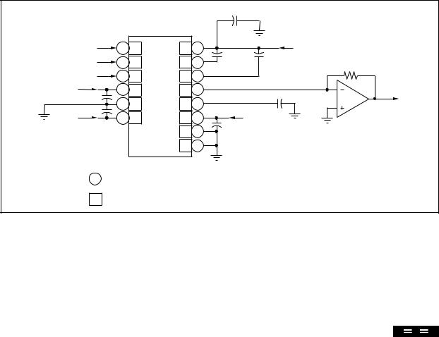
PIN ASSIGNMENTS (DIP Package)
PIN |
MNEMONIC |
PIN |
MNEMONIC |
|
|
|
|
1 |
DATA |
9 |
+VCC |
2 |
CLOCK |
10 |
BPO DC |
3 |
+VDD |
11 |
IOUT |
4 |
DCOM |
12 |
ACOM |
5 |
–VDD |
13 |
ACOM |
6 |
LE |
14 |
SERV DC |
7 |
NC |
15 |
REF DC |
8 |
NC |
16 |
–VCC |
|
|
|
|
PACKAGE INFORMATION(1)
|
|
PACKAGE DRAWING |
MODEL |
PACKAGE |
NUMBER |
|
|
|
PCM1702P |
16-Pin Plastic DIP |
180 |
PCM1702U |
20-Pin Plastic SOP |
248 |
|
|
|
NOTE: (1) For detailed drawing and dimension table, please see end of data sheet, or Appendix D of Burr-Brown IC Data Book.
PIN ASSIGNMENTS (SOP Package)
PIN |
MNEMONIC |
PIN |
MNEMONIC |
|
|
|
|
1 |
DATA |
11 |
+VCC |
2 |
CLOCK |
12 |
BPO DC |
3 |
NC |
13 |
NC |
4 |
+VDD |
14 |
IOUT |
5 |
DCOM |
15 |
ACOM |
6 |
–VDD |
16 |
ACOM |
7 |
LE |
17 |
SERV DC |
8 |
NC |
18 |
NC |
9 |
NC |
19 |
RFE DC |
10 |
NC |
20 |
–VCC |
|
|
|
|
GRADE MARKING (SOP Package)
MODEL |
PACKAGE |
|
|
PCM1702U |
Marked PCM1702. |
PCM1702U-J |
Marked with white dot by pin 10. |
PCM1702U-K |
Marked with red dot by pin 10. |
|
|
CONNECTION DIAGRAM
|
|
|
|
|
|
|
47µF |
|
|
|
|
|
|
|
|
|
+ |
|
|
CLOCK |
|
2 |
2 |
16 |
20 |
22µF |
100µF |
–5V VCC |
|
|
|
|
|
|
|
|
|
||
|
DATA |
|
1 |
1 |
15 |
19 |
+ |
+ |
RNF |
|
|
|
|
||||||
|
|
|
|
|
|
|
|
|
|
|
LE |
|
7 |
6 |
14 |
17 |
|
|
|
+5V VDD |
47µF |
+ |
4 |
3 |
11 |
14 |
|
47µF |
VOUT |
|
|
+ |
5 |
4 |
10 |
12 |
|
+ |
|
|
47µF |
|
|
|
|
|
|
||
–5V V |
|
6 |
5 |
9 |
11 |
|
+5V VCC |
|
|
|
|
+ |
|
||||||
DD |
|
|
|
|
|
|
|
|
|
|
|
|
|
|
13 |
16 |
47µF |
|
|
|
|
|
|
|
|
|
|
||
|
|
|
|
|
12 |
15 |
|
|
|
|
|
= SOP |
|
|
|
|
|
|
|
|
|
= DIP |
|
|
|
|
|
|
|


 ®
®
3 |
PCM1702 |
|
|
 Loading...