


PCM1732U
24-Bit, 96kHz, Stereo Audio
DIGITAL-TO-ANALOG CONVERTER
With HDCD® Decoder
49%
FPO
PCM1732
®
TM
FEATURES
● ENHANCED MULTI-LEVEL ∆Σ DAC
● INPUT AUDIO DATA WORD: 16-, 20-, 24-Bit
● SAMPLING FREQUENCY (fs): 16kHz - 96kHz
● SYSTEM CLOCK: 256, 384, 512, 768f
S
● HIGH PERFORMANCE:
THD+N: –96dB
Dynamic Range: 104dB
SNR: 104dB
● AUDIO OUTPUT LEVEL: 0.57 x VCC (Vp-p)
● 8x OVERSAMPLING DIGITAL FILTER WITH
HDCD DECODER:
Stopband Attenuation: –120dB
Passband Ripple: ±0.00001dB
HDCD Filter Optimized for 44.1kHz to 48kHz
and 88.2kHz to 96kHz
● MULTI-FUNCTIONS:
Digital De-emphasis
Soft Mute
Digital Attenuation
Zero Detect
Digital Gain Scaling
Reversible Output Phase
● +5V SINGLE-SUPPLY OPERATION
● SMALL SO-28 PACKAGE
© 1999 Burr-Brown Corporation PDS-1522B Printed in U.S.A. August, 1999
For most current data sheet and other product
information, visit www.burr-brown.com
®
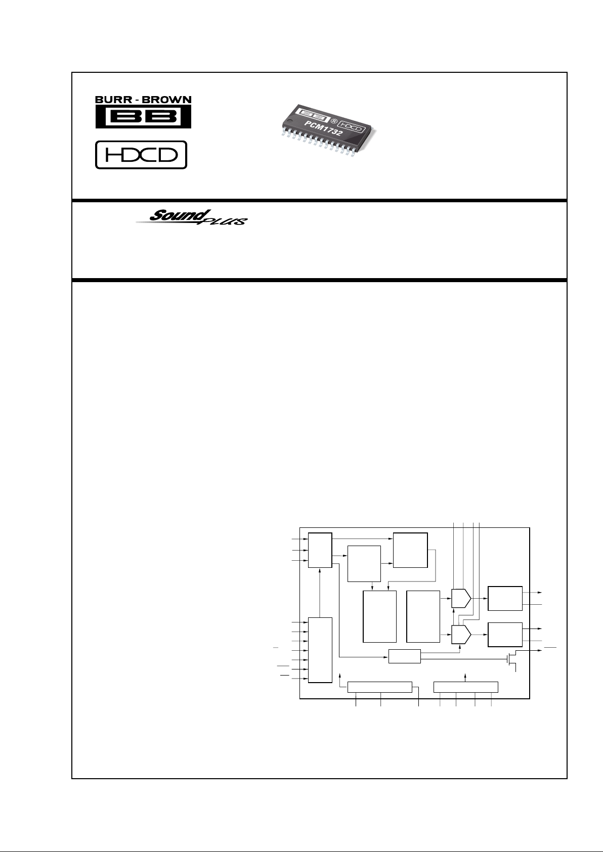
DESCRIPTION
The PCM1732 is designed for mid- to high-grade
digital audio applications which achieve 96kHz sampling rates with 24-bit audio data, such as High Definition Compatible Digital (HDCD) CD players, DVD
players, mini-disc players and AV receivers.
PCM1732 uses a newly-developed “enhanced, multilevel delta-sigma modulator” architecture that improves audio dynamic performance and reduces jitter
sensitivity.
The internal digital filter operates at 8x oversampling
at a 96kHz sampling rate, with –120dB stopband
attenuation.
International Airport Industrial Park • Mailing Address: PO Box 11400, Tucson, AZ 85734 • Street Address: 6730 S. Tucson Blvd., Tucson, AZ 85706 • Tel: (520) 746-1111
Twx: 910-952-1111 • Internet: http://www.burr-brown.com/ • Cable: BBRCORP • Telex: 066-6491 • FAX: (520) 889-1510 • Immediate Product Info: (800) 548-6132
®
HDCD® is a registered trademark of Pacific Microsonics, Inc.
HDCD
®
technology is provided under license from Pacific Microsonics
Inc. The PCM1732’s design is covered by the following patents:
In the USA: 45,479,168, 5,638,074, 5,640,161, 5,808,574, 5,838,274
5,854,600, 5,864,311, 5,872,531.
In Australia: 669,114.
Other patents pending.
Serial
Input
I/F
Mode
Control
I/F
HDCD
Hidden
Code
Recovery
HDCD
8x
Oversampling
Digital Filter
Enhanced
Multi-Level
∆Σ
Modulator
Crystal/OSC
XTI
SCK
XTO CLKO V
CC1
AGND1 VDDDGND
HDCD
Amplitude
Decoding
V
OUT
L
V
CC2
L
V
CC2
R
AGND2R
AGND2L
EXTL
PCM1732
Open
Drain
DAC
Low-Pass
Filter
Low-Pass
Filter
BPZ Control
V
OUT
R
EXTR
ZERO
DAC
ML/I2S
MC/DEM
MD/FSS
CS/IWO
MODE
MUTE
RST
LRCIN
DIN
BCKIN
Power Supply
Power-On Reset
NOTE: An HDCD license from Pacific Microsonics, Inc. is
required to purchase the PCM1732.
®
2
PCM1732
SPECIFICATIONS
24-Bit Data Performance
All specifications at +25°C, +VCC = +V
DD
= +5V, fS = 44.1kHz, and SYSCLK = 384fS, unless otherwise noted.
PCM1732
PARAMETER CONDITIONS MIN TYP MAX UNITS
RESOLUTION 24 Bits
DATA FORMAT
Audio Data Interface Format Standard/I
2
S
Data Bit Length 16/20/24 Selectable
Audio Data Format MSB-First, Binary Two’s Complement
Sampling Frequency (f
S
) 16 96 kHz
System Clock Frequency
(1)
256/384/512/768f
S
System Clock Duty Cycle 40 60 %
DIGITAL INPUT/OUTPUT LOGIC LEVEL
Input Logic Level (except XTI): V
IH
2.0 V
V
IL
0.8 V
Output Logic Level (CLKO): V
OH
I
OH
= 2mA 4.5 V
V
OL
I
OL
= 4mA 0.5 V
CLKO PERFORMANCE
(2)
Output Rise Time 20 ~ 80% VDD, 10pF 5.5 ns
Output Fall Time 80 ~ 20% V
DD
, 10pF 4 ns
Output Duty Cycle 10pF Load 30 %
DYNAMIC PERFORMANCE
(3, 4)
THD+N VO = 0dB fS = 44.1kHz –96 –90 dB
f
S
= 96kHz –94 dB
V
O
= –60dB fS = 44.1kHz –42 dB
Dynamic Range f
S
= 44.1kHz, EIAJ A-weighted 98 104 dB
f
S
= 96kHz, A-weighted 103 dB
Signal-to-Noise Ratio
(5)
fS = 44.1kHz, EIAJ A-weighted 98 104 dB
f
S
= 96kHz, A-weighted 103 dB
Channel Separation f
S
= 44.1kHz 96 104 dB
f
S
= 96kHz 101 dB
DC ACCURACY
Gain Error ±1.0 ±3.0 % of FSR
Gain Mismatch Channel-to-Channel ±1.0 ±3.0 % of FSR
Bipolar Zero Error V
O
= 0.5VCC at Bipolar Zero ±30 ±60 mV
ANALOG OUTPUT
Output Voltage
(6)
Full Scale (0dB) 0.57 V
CC
Vp-p
Center Voltage 0.5 V
CC
V
Load Impedance AC Load 5 kΩ
DIGITAL FILTER PERFORMANCE
Filter Characteristics 1
(f
S
= 44.1kHz/48kHz optimal)
Passband ±0.002dB 0.471f
S
–3dB 0.487f
S
Stopband 0.515f
S
Passband Ripple < 0.453f
S
±0.0001 dB
Stopband Attenuation Stopband = 0.515f
S
–109 dB
Stopband = 0.520f
S
–123 dB
Delay Time 81/f
S
sec
Filter Characteristics 2
(f
S
= 88.2kHz/96kHz optimal)
Passband ±0.005dB 0.395f
S
–3dB 0.441f
S
Stopband 0.538f
S
Passband Ripple < 0.341f
S
±0.0001 dB
Stopband Attenuation Stopband = 0.538f
S
–132 dB
Delay Time 31/f
S
sec
De-Emphasis Error ±0.1 dB
INTERNAL ANALOG FILTER
–3dB Bandwidth 100 kHz
Passband Response f = 20kHz –0.16 dB
POWER SUPPLY REQUIREMENTS
Voltage Range V
DD, VCC
4.5 5 5.5 VDC
Supply Current: I
CC
+ I
DD
fS = 44.1kHz 85 105 mA
f
S
= 96kHz 93 mA
Power Dissipation f
S
= 44.1kHz 425 525 mW
f
S
= 96kHz 465 mW
TEMPERATURE RANGE
Operating –25 +70 °C
Storage –55 +100 °C
Thermal Resistance,
θ
JA
67 °C/W
NOTES: (1) Refer to the System Clock section of this data sheet. (2) An external buffer is recommended. (3) Dynamic performance specifications are tested with 20kHz low-pass
filter and THD+N specifications are tested with 30kHz LPF, 400Hz HPF, Average Mode. (4) Dynamic performance specifications are tested with HDCD gain scaling set to analog
gain scaling. (5) SNR is tested with infinite zero detection off. (6) Output level is for sine wave. DAC outputs 0.64 V
CC
(peak-to-peak) due to filter response as transient.
®
3 PCM1732
SPECIFICATIONS
16-Bit Data Performance
All specifications at +25°C, +VDD = +V
CC
= +5V, fS = 44.1kHz, and SYSCLK = 384fS, unless otherwise noted. For discussion of HDCD scaling options, see the
Applications Considerations section of this data sheet.
PCM1732U
PARAMETER CONDITIONS MIN TYP MAX UNITS
DYNAMIC ANALOG PERFORMANCE,
STANDARD CD, ANALOG HDCD SCALING
(1)
Total Harmonic Distortion + Noise
V
O
= 0dB 0dBFS –95 dB
V
O
= –60dB –37 dB
Dynamic Range EIAJ A-Weighted 99 dB
Output Voltage, Sine Wave 0dBFS
(2)
0.57V
CC
Vp-p
DYNAMIC ANALOG PERFORMANCE,
HDCD CD, ANALOG HDCD SCALING
(3)
Total Harmonic Distortion + Noise
VO = 0dB 0dBFS –94 dB
V
O
= –60dB –38 dB
Dynamic Range EIAJ A-Weighted
(4)
104 dB
Output Voltage, Sine Wave 0dBFS, Without Peak Extend
(2)
0.57V
CC
Vp-p
0dBFS, With Peak Extend
(5)
0.285V
CC
Vp-p
+6dBFS
(5, 6)
0.57V
CC
Vp-p
DYNAMIC ANALOG PERFORMANCE,
Standard CD, Digital HDCD SCALING
(1)
Total Harmonic Distortion + Noise
V
O
= 0dB 0dBFS –92 dB
V
O
= –60dB –33 dB
Dynamic Range EIAJ A-Weighted 96 dB
Output Voltage, Sine Wave 0dBFS 0.285V
CC
Vp-p
DYNAMIC ANALOG PERFORMANCE
HDCD CD, Digital HDCD SCALING
(2)
Total Harmonic Distortion + Noise
VO = 0dB 0dBFS –91 dB
V
O
= –60dB –34 dB
Dynamic Range EIAJ A-Weighted
(4)
104 dB
Output Voltage, Sine Wave 0dBFS 0.285V
CC
Vp-p
+6dBFS
(5)
0.57V
CC
Vp-p
NOTES: (1) Without dither. (2) Gain pin is LOW. (3) With the rectangular PDF dither. (4) Including Peak Extend to +6dBFS. (5) Gain pin is HIGH. (6) +6dBFS is
the full Peak Extend, while dynamic range numbers are with Peak Extend.
The information provided herein is believed to be reliable; however, BURR-BROWN assumes no responsibility for inaccuracies or omissions. BURR-BROWN assumes
no responsibility for the use of this information, and all use of such information shall be entirely at the user’s own risk. Prices and specifications are subject to change
without notice. No patent rights or licenses to any of the circuits described herein are implied or granted to any third party. BURR-BROWN does not authorize or warrant
any BURR-BROWN product for use in life support devices and/or systems.
®
4
PCM1732
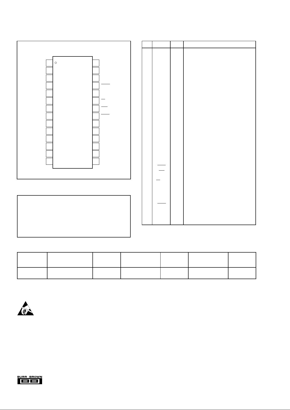
PIN NAME I/O DESCRIPTION
1 LRCIN IN Left and Right Clock Input. This clock is equal to
the sampling rate, fS.
(1)
2 DIN IN Serial Audio Data Input
(1)
3 BCKIN IN Bit Clock Input for Serial Audio Data
(1)
4 CLKO OUT Buffered System Clock Output.
5 XTI IN Oscillator Input/External Clock Input
(2)
6 XTO OUT Oscillator Output
7 DGND — Digital Ground
8V
DD
— Digital Power +5V
9 HDCD OUT HDCD Encoded Data Detect
10 V
CC
2R — Analog Power +5V, Rch
11 AGND2R — Analog Ground, Rch
12 EXTR — Common Mode Voltage for Analog Output Amp,
Rch
13 V
OUT
R OUT Analog Voltage Output, Rch
14 AGND1 — Analog Ground
15 V
CC
1 — Analog Power +5V
16 V
OUT
L OUT Analog Voltage Output, Lch
17 EXTL — Common Mode Voltage for Analog Output Amp,
Lch
18 AGND2L OUT Analog Ground, Lch
19 V
CC
2L — Analog Power +5V, Lch
20 GAIN OUT External (analog) Gain Scaling
21 ZERO OUT Zero Data Flag
22 RST IN Reset. When this pin is LOW, the digital filter
and modulators are held in reset.
(3)
23 CS/IW0 IN Chip Select/Input Format Selection. When this
pin is LOW, the Mode Control interface is enabled.
(4)
24 MODE IN
Mode Control Select: H = Software; L =
Hardware
(3)
25 MUTE IN Mute Control
(3)
26 MD/FSS IN Mode Data/Sampling Rate Range Select
(3)
27
MC/DEM
IN Mode Clock/De-Emphasis Select
(3)
28 ML/I2S IN Mode Latch/Input Format Select
(3)
NOTES: (1) Schmitt Trigger input. (2) CMOS logic level input. (3) Schmitt
Trigger input with pull-up resister. (4) Schmitt Trigger input with pull-down
resistor.
PIN ASSIGNMENTSPIN CONFIGURATION
ELECTROSTATIC
DISCHARGE SENSITIVITY
This integrated circuit can be damaged by ESD. Burr-Brown
recommends that all integrated circuits be handled with
appropriate precautions. Failure to observe proper handling
and installation procedures can cause damage.
ESD damage can range from subtle performance degradation
to complete device failure. Precision integrated circuits may
be more susceptible to damage because very small parametric
changes could cause the device not to meet its published
specifications.
Power Supply Voltage ...................................................................... +6.5V
+V
CC
to +VDD Difference ................................................................... ±0.1V
Input Logic Voltage .................................................. –0.3V to (V
DD
+ 0.3V)
Input Current (except power supply)............................................... ±10mA
Power Dissipation .......................................................................... 750mW
Operating Temperature Range ......................................... –25°C to +70°C
Storage Temperature...................................................... –55°C to +125°C
Lead Temperature (soldering, 5s)................................................. +260°C
(reflow, 10s) .................................................... +235°C
ABSOLUTE MAXIMUM RATINGS
LRCIN
DIN
BCKIN
CLKO
XTI
XTO
DGND
V
DD
HDCD
V
CC
2R
AGND2R
EXTR
V
OUT
R
AGND1
ML/I
2
S
MC/DEM
MD/FSS
MUTE
MODE
CS/IWO
RST
ZERO
GAIN
V
CC
2L
AGND2L
EXTL
V
OUT
L
V
CC
1
1
2
3
4
5
6
7
8
9
10
11
12
13
14
28
27
26
25
24
23
22
21
20
19
18
17
16
15
PCM1732U
Top View SO-28
PACKAGE SPECIFIED
DRAWING TEMPERATURE PACKAGE ORDERING TRANSPORT
PRODUCT PACKAGE NUMBER
(1)
RANGE MARKING NUMBER
(2)
MEDIA
PCM1732U SO-28 217 –25°C to +70°C PCM1732U PCM1732U Rails
"""""PCM1732U/1K Tape and Reel
NOTES: (1) For detailed drawing and dimension table, please see end of data sheet, or Appendix C of Burr-Brown IC Data Book. (2) Models with a slash (/ ) are
available only in Tape and Reel in the quantities indicated (e.g., /1K indicates 1000 devices per reel). Ordering 1000 pieces of “PCM1732U/1K” will get a single
1000-piece Tape and Reel. For detailed Tape and Reel mechanical information, refer to Appendix B of Burr-Brown IC Data Book.
PACKAGE/ORDERING INFORMATION
®
5 PCM1732
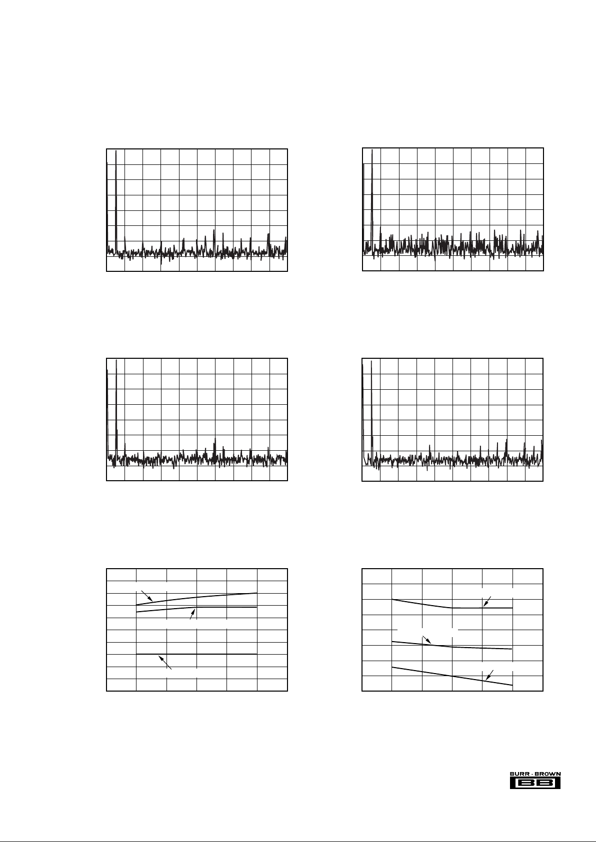
TYPICAL PERFORMANCE CURVES
All specifications at +25°C, +VCC = +V
DD
= +5V, fS = 44.1kHz, and 24-bit input data, SYSCLK = 384fS, unless otherwise noted.
108
107
106
105
104
103
102
101
100
99
98
DYNAMIC RANGE vs SUPPLY VOLTAGE
Power Supply Voltage (V)
4.25 4.50 4.75 5.00 5.25 5.50 5.75
Dynamic Range (dB)
fS = 44.1kHz, 24-Bit
fS = 44.1kHz, 16-Bit
HDCD with Peak Extend
–86
–88
–90
–92
–94
–96
98
100
–102
THD+N vs SUPPLY VOLTAGE
Power Supply Voltage (V)
4.25 4.50 4.75 5.00 5.25 5.50 5.75
THD+N at 0dB (dB)
fS = 44.1kHz, 16-Bit
HDCD With Peak Extend
fS = 44.1kHz, 24-Bit
–60
–70
–80
–90
–100
–110
–120
–130
–140
0246810
Frequency (kHz)
–60dB AMPLITUDE vs FREQUENCY
24-Bit Data
Amplitude (dB)
12 14 16 18 20
–60
–70
–80
–90
–100
–110
–120
–130
–140
–60dB AMPLITUDE vs FREQUENCY
16-Bit Data
Frequency (kHz)
0 2 4 6 8 101214161820
Amplitude (dB)
–60
–70
–80
–90
–100
–110
–120
–130
–140
–60dB AMPLITUDE vs FREQUENCY
HDCD Without Peak Extend
Frequency (kHz)
0 2 4 6 8 101214161820
Amplitude (dB)
–60
–70
–80
–90
–100
–110
–120
–130
–140
–60dB AMPLITUDE vs FREQUENCY
HDCD With Peak Extend
Frequency (kHz)
0 2 4 6 8 101214161820
Amplitude (dB)
®
6
PCM1732
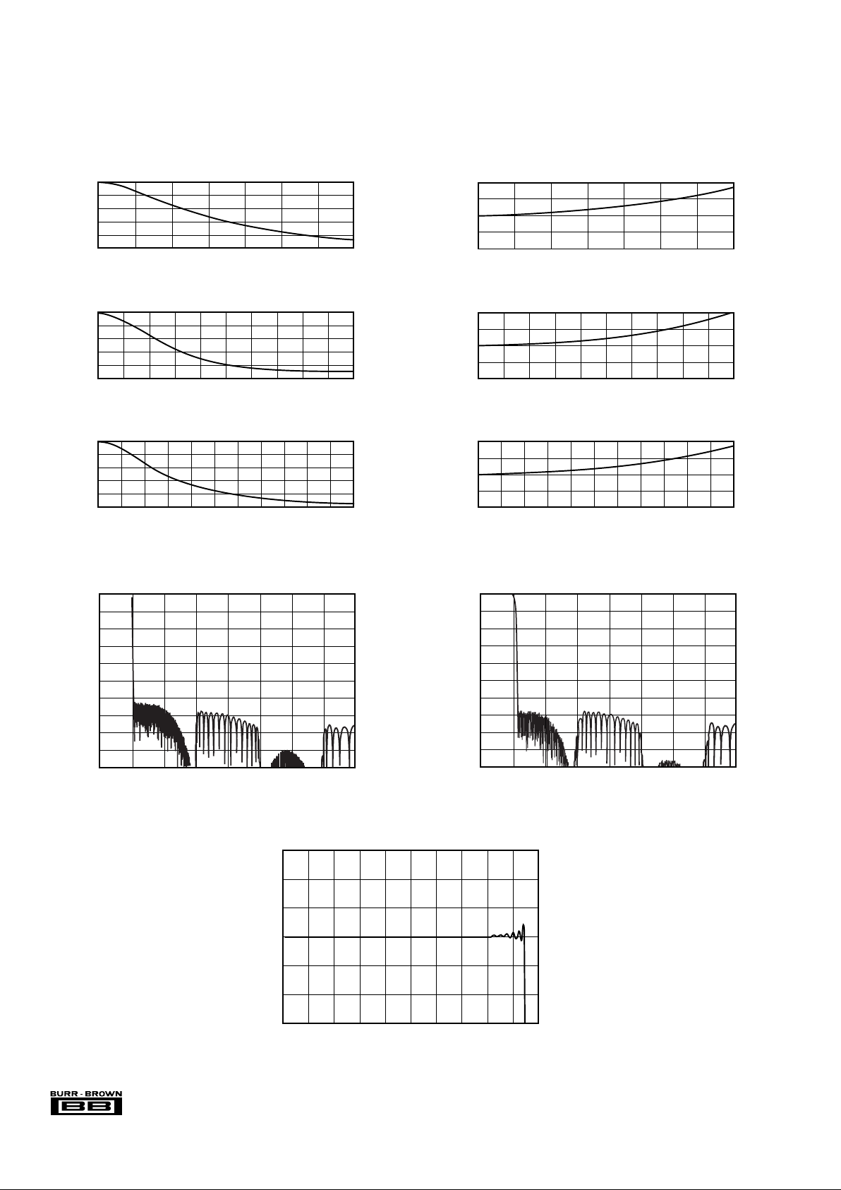
TYPICAL PERFORMANCE CURVES
DIGITAL FILTER
06
Frequency (kHz)
DE-EMPHASIS FREQUENCY RESPONSE (32kHz)
Level (dB) Level (dB)
DE-EMPHASIS FREQUENCY RESPONSE (44.1kHz)
02468101214161820
0
–2
–4
–6
–8
–10
Level (dB)
DE-EMPHASIS FREQUENCY RESPONSE (48kHz)
0 2 4 6 8 10121416182022
Frequency (kHz)
0
–2
–4
–6
–8
–10
0
2
4 6 8 10 12 14
Frequency (kHz)
0
–2
–4
–6
–8
–10
Level (dB)
0
DE-EMPHASIS ERROR (32kHz)
DE-EMPHASIS ERROR (44.1kHz)
DE-EMPHASIS ERROR (48kHz)
0 2 4 6 8 10121416182022
Frequency (kHz)
2
468101214
Frequency (kHz)
0.02
0.01
0
–0.01
–0.02
0
2
4 6 8 101214161820
Level (dB)
0.02
0.01
0
–0.01
–0.02
Level (dB)
0.04
0.02
0
–0.02
–0.04
Level (dB)
0
–20
–40
–60
–80
–100
–120
–140
–160
–180
–200
FREQUENCY RESPONSE
(De-Emphasis Off, f
S
= 44.1kHz)
Frequency (x f
S
Hz)
0 3.50.5 1.0 1.5 2.0 2.5 3.0 4.0
Amplitude (dB)
0
–20
–40
–60
–80
–100
–120
–140
–160
–180
–200
FREQUENCY RESPONSE
(FSS High, 96kHz Filter)
Frequency (x f
S
Hz)
0 3.50.5 1.0 1.5 2.0 2.5 3.0 4.0
Amplitude (dB)
0.003
0.002
0.001
0
–0.001
–0.002
–0.003
PASSBAND RIPPLE CHARACTERISTICS
Frequency (x f
S
Hz)
0 0.05 0.1 0.15 0.2 0.25 0.3 0.35 0.4 0.45 0.5
Amplitude (dB)
 Loading...