


Burr Brown INA2126UA-2K5, INA2126UA, INA2126PA, INA2126EA-250, INA2126E-2K5 Datasheet
...


 ®
®
 INA126
 INA126
INA2126
INA2126
 INA2126
INA126
INA2126
MicroPOWER INSTRUMENTATION AMPLIFIER
Single and Dual Versions
FEATURES
●LOW QUIESCENT CURRENT: 175μA/chan.
●WIDE SUPPLY RANGE: ±1.35V to ±18V
●LOW OFFSET VOLTAGE: 250μV max
●LOW OFFSET DRIFT: 3μV/°C max
●LOW NOISE: 35nV/Ö Hz
●LOW INPUT BIAS CURRENT: 25nA max
●8-PIN DIP, SO-8, MSOP-8 SURFACEMOUNT DUAL: 16-Pin DIP, SO-16, SSOP-16
DESCRIPTION
The INA126 and INA2126 are precision instrumentation amplifiers for accurate, low noise differential signal acquisition. Their two-op-amp design provides excellent performance with very low quiescent current (175mA/chan.). This, combined with wide operating voltage range of ±1.35V to
±18V, makes them ideal for portable instrumentation and data acquisition systems.
Gain can be set from 5V/V to 10000V/V with a single external resistor. Laser trimmed input circuitry provides low offset voltage (250mV max), low offset voltage drift (3mV/°C max) and excellent common-mode rejection.
APPLICATIONS
●INDUSTRIAL SENSOR AMPLIFIER: Bridge, RTD, Thermocouple
●PHYSIOLOGICAL AMPLIFIER: ECG, EEG, EMG
●MULTI-CHANNEL DATA ACQUISITION
●PORTABLE, BATTERY OPERATED SYSTEMS
VIN+ 3
8
RG
1
VIN– 2
V+ |
|
|
|
|
|
7 |
|
|
|
|
|
INA126 |
|
|
|
|
|
|
6 |
|
= (V |
+ |
– V–) G |
|
V |
O |
|||
|
|
|
IN |
IN |
|
40kΩ |
|
|
G = 5 + 80k |
||
|
|
|
|
|
RG |
10kΩ |
|
|
|
|
|
10kΩ |
|
|
|
|
|
40kΩ |
5 |
|
|
|
|
|
|
|
|
|
|
4 |
|
|
|
|
|
V– |
|
|
|
|
|
Single version package options include 8-pin plastic DIP, SO-8 surface mount, and fine-pitch MSOP-8 surface-mount. Dual version is available in the space-saving SSOP-16 finepitch surface mount, SO-16, and 16-pin DIP. All are specified for the –40°C to +85°C industrial temperature range.
|
|
|
|
V+ |
|
|
|
|
VIN+ |
2 |
INA2126 |
9 |
|
|
|
|
|
|
6 |
|
|
= (V + |
|
–) G |
||
|
4 |
|
V |
O |
– V |
|||
|
40kΩ |
|
|
IN |
IN |
|||
|
|
7 |
|
|
G = 5 + |
80k |
||
|
|
10kΩ |
|
|
RG |
|||
|
RG |
|
|
|
|
|
|
|
|
|
|
|
|
|
|
|
|
|
3 |
10kΩ |
|
|
|
|
|
|
VIN– |
1 |
40kΩ |
|
|
|
|
|
|
|
|
5 |
|
|
|
|
|
|
|
|
|
|
|
|
|
|
|
VIN+ |
15 |
|
11 |
|
|
= (V+ |
|
–) G |
|
|
|
V |
|
– V |
|||
|
13 |
|
|
O |
||||
|
40kΩ |
|
|
IN |
|
IN |
||
|
|
|
|
|
G = 5 + |
80k |
||
|
|
10kΩ |
10 |
|
|
|
|
RG |
|
RG |
|
|
|
|
|
||
|
|
|
|
|
|
|
|
|
|
14 |
10kΩ |
|
|
|
|
|
|
VIN– |
16 |
40kΩ |
|
|
|
|
|
|
|
8 |
12 |
|
|
|
|
|
|
|
|
|
|
|
|
|
||
|
V– |
|
|
|
|
|
|
|
International Airport Industrial Park • Mailing Address: PO Box 11400, Tucson, AZ 85734 • Street Address: 6730 S. Tucson Blvd., Tucson, AZ 85706 • Tel: (520) 746-1111 • Twx: 910-952-1111 Internet: http://www.burr-brown.com/ • FAXLine: (800) 548-6133 (US/Canada Only) • Cable: BBRCORP • Telex: 066-6491 • FAX: (520) 889-1510 • Immediate Product Info: (800) 548-6132
© 1996 Burr-Brown Corporation PDS-1365C Printed in U.S.A. September, 1997

SPECIFICATIONS
At TA = +25°C, VS = ±15V, RL = 25kW, unless otherwise noted.
|
|
|
INA126P, U, E |
|
INA126PA, UA, EA |
|
|
|
|
|
|
|
|
|
|||||
|
|
|
INA2126P, U, E |
INA2126PA, UA, EA |
|
|
|
|
|
|
|
|
|||||||
|
|
|
|
|
|
|
|
|
|
|
|
|
|
|
|
|
|
|
|
PARAMETER |
CONDITIONS |
MIN |
|
TYP |
|
MAX |
MIN |
TYP |
|
MAX |
UNITS |
||||||||
|
|
|
|
|
|
|
|
|
|
|
|
|
|
|
|
|
|
|
|
INPUT |
|
|
|
|
|
|
|
|
|
|
|
|
|
|
|
|
|
|
|
Offset Voltage, RTI |
|
|
|
|
±100 |
|
±250 |
|
±150 |
|
±500 |
mV |
|||||||
vs Temperature |
|
|
|
|
±0.5 |
|
±3 |
|
|
|
±5 |
mV/°C |
|||||||
vs Power Supply (PSRR) |
VS = ±1.35V to ±18V |
|
|
|
5 |
|
15 |
|
|
|
50 |
mV/V |
|||||||
Input Impedance |
|
|
|
|
109 || 4 |
|
|
|
|
|
|
W || pF |
|||||||
Safe Input Voltage |
RS = 0 |
(V–)–0.5 |
|
|
|
(V+)+0.5 |
|
|
|
|
V |
||||||||
|
RS = 1kW |
(V–)–10 |
|
|
|
(V+)+10 |
|
|
|
|
V |
||||||||
Common-Mode Voltage Range |
VO = 0V |
±11.25 |
|
±11.5 |
|
|
|
|
|
|
V |
||||||||
Channel Separation (dual) |
G = 5, dc |
|
|
|
130 |
|
|
|
|
|
|
dB |
|||||||
Common-Mode Rejection |
RS = 0, VCM = ±11.25V |
83 |
|
|
94 |
|
|
74 |
90 |
|
|
dB |
|||||||
INA2126U (dual SO-16) |
|
80 |
|
|
94 |
|
|
|
|
|
|
dB |
|||||||
|
|
|
|
|
|
|
|
|
|
|
|
|
|
|
|
|
|
|
|
INPUT BIAS CURRENT |
|
|
|
|
–10 |
|
–25 |
|
|
|
–50 |
nA |
|||||||
vs Temperature |
|
|
|
|
±30 |
|
|
|
|
|
|
pA/°C |
|||||||
Offset Current |
|
|
|
|
±0.5 |
|
±2 |
|
|
|
±5 |
nA |
|||||||
vs Temperature |
|
|
|
|
±10 |
|
|
|
|
|
|
pA/°C |
|||||||
GAIN |
|
|
|
G = 5 to 10k |
|
|
|
|
|
V/V |
|||||||||
Gain Equation |
|
|
G = 5 + 80kW/RG |
|
|
|
|
V/V |
|||||||||||
Gain Error |
VO = ±14V, G = 5 |
|
|
|
±0.02 |
|
±0.1 |
|
|
|
±0.18 |
% |
|
|
|
|
|||
vs Temperature |
G = 5 |
|
|
|
±2 |
|
±10 |
|
|
|
|
ppm/°C |
|||||||
Gain Error |
VO = ±12V, G = 100 |
|
|
|
±0.2 |
|
±0.5 |
|
|
|
±1 |
% |
|
|
|
|
|||
vs Temperature |
G = 100 |
|
|
|
±25 |
|
±100 |
|
|
|
|
ppm/°C |
|||||||
Nonlinearity |
G = 100, VO = ±14V |
|
|
|
±0.002 |
|
±0.012 |
|
|
|
|
% |
|
|
|
|
|||
NOISE |
|
|
|
|
|
|
|
|
|
|
|
|
|
|
|
|
|
|
|
Voltage Noise, f = 1kHz |
|
|
|
|
35 |
|
|
|
|
|
|
nV/Ö |
|
|
|
|
|
||
|
|
|
|
|
|
|
|
|
|
Hz |
|||||||||
f = 100Hz |
|
|
|
|
35 |
|
|
|
|
|
|
nV/Ö |
Hz |
|
|||||
f = 10Hz |
|
|
|
|
45 |
|
|
|
|
|
|
nV/Ö |
|
|
|
||||
|
|
|
|
|
|
|
|
|
|
Hz |
|||||||||
fB = 0.1Hz to 10Hz |
|
|
|
|
0.7 |
|
|
|
|
|
|
mVp-p |
|||||||
Current Noise, f = 1kHz |
|
|
|
|
60 |
|
|
|
|
|
|
fA/Ö |
Hz |
|
|||||
fB = 0.1Hz to 10Hz |
|
|
|
|
2 |
|
|
|
|
|
|
pAp-p |
|||||||
OUTPUT |
|
|
|
|
|
|
|
|
|
|
|
|
|
|
|
|
|
|
|
Voltage, Positive |
RL = 25kW |
(V+)–0.9 |
|
(V+)–0.75 |
|
|
|
|
|
|
V |
||||||||
Negative |
RL = 25kW |
(V–)+0.95 |
|
(V–)+0.8 |
|
|
|
|
|
|
V |
||||||||
Short-Circuit Current |
Short-Circuit to Ground |
|
|
|
+10/–5 |
|
|
|
|
|
|
mA |
|||||||
Capacitive Load Drive |
|
|
|
|
1000 |
|
|
|
|
|
|
pF |
|||||||
|
|
|
|
|
|
|
|
|
|
|
|
|
|
|
|
|
|
|
|
FREQUENCY RESPONSE |
|
|
|
|
|
|
|
|
|
|
|
|
|
|
|
|
|
|
|
Bandwidth, –3dB |
G = 5 |
|
|
|
200 |
|
|
|
|
|
|
kHz |
|||||||
|
G = 100 |
|
|
|
9 |
|
|
|
|
|
|
kHz |
|||||||
|
G = 500 |
|
|
|
1.8 |
|
|
|
|
|
|
kHz |
|||||||
Slew Rate |
VO = ±10V, G = 5 |
|
|
|
0.4 |
|
|
|
|
|
|
V/ms |
|||||||
Settling Time, 0.01% |
10V Step, G = 5 |
|
|
|
30 |
|
|
|
|
|
|
ms |
|||||||
|
10V Step, G = 100 |
|
|
|
160 |
|
|
|
|
|
|
ms |
|||||||
|
10V Step, G = 500 |
|
|
|
1500 |
|
|
|
|
|
|
ms |
|||||||
Overload Recovery |
50% Input Overload |
|
|
|
4 |
|
|
|
|
|
|
ms |
|||||||
POWER SUPPLY |
|
|
|
|
|
|
|
|
|
|
|
|
|
|
|
|
|
|
|
Voltage Range |
|
±1.35 |
|
|
±15 |
|
±18 |
|
|
|
|
V |
|||||||
Current (per channel) |
IO = 0 |
|
|
|
±175 |
|
±200 |
|
|
|
|
mA |
|||||||
TEMPERATURE RANGE |
|
|
|
|
|
|
|
|
|
|
|
|
|
|
|
|
|
|
|
Specification Range |
|
–40 |
|
|
|
+85 |
|
|
|
|
°C |
||||||||
Operation Range |
|
–55 |
|
|
|
+125 |
|
|
|
|
°C |
||||||||
Storage Range |
|
–55 |
|
|
|
+125 |
|
|
|
|
°C |
||||||||
Thermal Resistance, θJA |
|
|
|
|
|
|
|
|
|
|
|
|
|
|
|
|
|
|
|
8-Pin DIP |
|
|
|
|
100 |
|
|
|
|
|
|
°C/W |
|||||||
SO-8 Surface-Mount |
|
|
|
|
150 |
|
|
|
|
|
|
°C/W |
|||||||
MSOP-8 Surface-Mount |
|
|
|
|
200 |
|
|
|
|
|
|
°C/W |
|||||||
16-Pin DIP (dual) |
|
|
|
|
80 |
|
|
|
|
|
|
°C/W |
|||||||
SO-16 (dual) |
|
|
|
|
100 |
|
|
|
|
|
|
°C/W |
|||||||
SSOP-16 (dual) |
|
|
|
|
100 |
|
|
|
|
|
|
°C/W |
|||||||
|
|
|
|
|
|
|
|
|
|
|
|
|
|
|
|
|
|
|
|
Specification same as INA126P, INA126U, INA126E; INA2126P, INA2126U, INA2126E.
The information provided herein is believed to be reliable; however, BURR-BROWN assumes no responsibility for inaccuracies or omissions. BURR-BROWN assumes no responsibility for the use of this information, and all use of such information shall be entirely at the user’s own risk. Prices and specifications are subject to change without notice. No patent rights or licenses to any of the circuits described herein are implied or granted to any third party. BURR-BROWN does not authorize or warrant any BURR-BROWN product for use in life support devices and/or systems.


 ®
®
|
INA126, INA2126 |
2 |
|
PIN CONFIGURATION (Single)
Top View |
|
|
8-Pin DIP, SO-8, MSOP-8 |
||
|
|
|
|
|
|
|
|
|
|
|
|
RG |
1 |
|
8 |
RG |
|
V– |
|
|
|
|
|
2 |
|
7 |
V+ |
||
IN |
|
|
|
|
|
V+ |
|
|
|
|
|
3 |
|
6 |
V |
O |
|
IN |
|
|
|
|
|
|
|
|
|
|
|
V– |
4 |
|
5 |
Ref |
|
|
|
|
|
|
|
|
|
|
|
|
|
|
|
|
|
|
|
ABSOLUTE MAXIMUM RATINGS(1)
........................................................Power Supply Voltage, V+ to V– |
36V |
Input Signal Voltage(2) ........................................... |
(V–)–0.7 to (V+)+0.7V |
Input Signal Current(2) ...................................................................... |
10mA |
Output Short Circuit ................................................................. |
Continuous |
Operating Temperature ................................................. |
–55°C to +125°C |
Storage Temperature ..................................................... |
–55°C to +125°C |
Lead Temperature (soldering, 10s) ............................................... |
+300°C |
|
|
NOTES: (1) Stresses above these ratings may cause permanent damage.
(2) Input signal voltage is limited by internal diodes connected to power supplies. See text.
PIN CONFIGURATION (Dual)
Top View |
|
16-Pin DIP, SO-16, SSOP-16 |
||
V– |
|
|
|
V– |
|
|
|
||
1 |
|
16 |
||
INA |
|
|
|
INB |
V+ |
|
|
|
V+ |
2 |
|
15 |
||
INA |
|
|
|
INB |
|
|
|
|
|
RGA |
3 |
|
14 |
RGB |
|
|
|
|
|
RGA |
4 |
|
13 |
RGB |
|
|
|
|
|
RefA |
5 |
|
12 |
RefB |
|
|
|
11 |
|
VOA |
6 |
|
VOB |
|
SenseA |
7 |
|
10 |
SenseB |
|
|
|
9 |
|
V– |
8 |
|
V+ |
|
|
|
|
|
|
|
|
|
|
|
|
|
|
|
|
PACKAGE INFORMATION
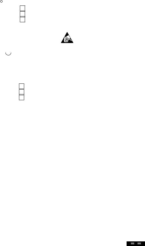
ELECTROSTATIC DISCHARGE SENSITIVITY
This integrated circuit can be damaged by ESD. Burr-Brown recommends that all integrated circuits be handled with appropriate precautions. Failure to observe proper handling and installation procedures can cause damage.
ESD damage can range from subtle performance degradation to complete device failure. Precision integrated circuits may be more susceptible to damage because very small parametric changes could cause the device not to meet its published specifications.
|
|
PACKAGE DRAWING |
|
|
TRANSPORT |
PRODUCT |
PACKAGE |
NUMBER(1) |
PACKAGE MARKING |
ORDERING NUMBER |
MEDIA |
Single |
|
|
|
|
|
|
|
|
|
|
|
INA126PA |
8-Pin DIP |
006 |
INA126PA |
INA126PA |
Rails |
INA126P |
8-Pin DIP |
006 |
INA126P |
INA126P |
Rails |
INA126UA |
SO-8 |
182 |
INA126UA |
INA126UA |
Rails or Reel |
INA126U |
SO-8 |
182 |
INA126U |
INA126U |
Rails or Reel |
|
|
|
|
|
|
INA126EA(2) |
MSOP-8 |
337 |
A26(3) |
INA126EA-250 |
Reel Only |
" |
" |
" |
" |
INA126EA-2500 |
" |
INA126E(2) |
MSOP-8 |
337 |
A26(3) |
INA126E-250 |
Reel Only |
" |
" |
" |
" |
INA126E-2500 |
" |
Dual |
|
|
|
|
|
|
|
|
|
|
|
INA2126PA |
16-Pin DIP |
180 |
INA2126PA |
INA2126PA |
Rails |
INA2126P |
16-Pin DIP |
180 |
INA2126P |
INA2126P |
Rails |
|
|
|
|
|
|
INA2126UA |
SO-16 |
265 |
INA2126UA |
INA2126UA |
Rails |
INA2126U |
SO-16 |
265 |
INA2126U |
INA2126U |
Rails |
|
|
|
|
|
|
INA2126EA(2) |
SSOP-16 |
322 |
INA2126EA |
INA2126EA-250 |
Reel Only |
" |
" |
" |
" |
INA2126EA-2500 |
" |
INA2126E(2) |
SSOP-16 |
322 |
INA2126E |
INA2126E-250 |
Reel Only |
" |
" |
" |
" |
INA2126E-2500 |
" |
|
|
|
|
|
|
NOTES: (1) For detailed drawing and dimension table, see end of data sheet, or Appendix C of Burr-Brown IC Data Book. (2) MSOP-8 and SSOP-16 packages are available only on 250 or 2500 piece reels. (3) Grade designation is marked on reel.


 ®
®
3 |
INA126, INA2126 |
|
|
 Loading...