

Page 1

R
WORD PROCESSOR
SERVICE MANUAL
MODEL:DP-525CJ/DP-530CJ/DP-540CJ/DP-550CJ
LW-800ic/LW-810ic/LW-810icBL/LW-840ic
REVISED EDITION
Page 2

SERVICE MANUAL
CONTENTS
PART I THEORY OF OPERATION
CHAPTER 1 MECHANICAL THEORY....................................................................... 1-1
1. Ink Jet Printer........................................................................................................... 1-1
1.1. Ink Jet Printer System Configuration .......................................................................... 1-2
1.2. Ink Jet Operation........................................................................................................1-4
1.2.1. Paper Feed Mechanism ................................................................................ 1-4
1.2.2. Carriage Assembly ....................................................................................... 1-7
1.2.3. Carriage Motion Control.............................................................................. 1-10
1.2.4. Maintenance Station Operation................................................................... 1-11
1.2.4.1. Spitting ................................................................................................. 1-12
1.2.4.2. Wiping.................................................................................................. 1-13
1.2.4.3. Capping................................................................................................ 1-14
1.2.4.4. Purging................................................................................................. 1-14
1.2.5. Sensors...................................................................................................... 1-15
1.2.5.1. Carriage Home Position Sensor............................................................ 1-15
1.2.5.2. PE Sensor ............................................................................................ 1-16
1.3. INK CHG (Ink Change) Functions.............................................................................1-17
1.3.1. Ink Cartridge Installation/Replacement ....................................................... 1-17
1.3.2. Automatic Print head Cleaning (Purging).................................................... 1-17
2. Keyboard ................................................................................................................ 1-18
CHAPTER 2 ELECTRICAL THEORY........................................................................ 2-1
1. System Configuration...............................................................................................2-1
1.1. Main PCB (Printed Circuit Board)............................................................................... 2-1
1.2. Switch PCB (Printed Circuit Board)............................................................................. 2-1
1.3. Keyboard FPC (Flexible Printed Circuit)..................................................................... 2-1
1.4. FDD (Floppy Disk Drive) Module................................................................................ 2-1
1.5. CRT Display............................................................................................................... 2-1
2. Ink Jet Printer Configuration.....................................................................................2-3
2.1. Ink Cartridge............................................................................................................... 2-3
2.2. Carriage Motor ........................................................................................................... 2-3
2.3. Line Feed Motor......................................................................................................... 2-3
2.4. Carriage Home Position Sensor.................................................................................. 2-3
2.5. PE (Paper End) Sensor ..............................................................................................2-3
i
Page 3

SERVICE MANUAL
3. Power Supply Circuit................................................................................................ 2-4
3.1. Configuration.............................................................................................................. 2-4
3.2. +24V Generator.......................................................................................................... 2-5
3.3. +5V Generator............................................................................................................ 2-5
4. Reset Circuit.............................................................................................................2-6
4.1. Configuration.............................................................................................................. 2-6
5. CBIC and Peripherals............................................................................................... 2-7
5.1. CBIC #9 ..................................................................................................................... 2-7
5.2. Main ROM (#12, #13)................................................................................................. 2-7
5.3. Main RAM (#10, #11) ................................................................................................. 2-7
5.4. Video RAM (#7) .......................................................................................................... 2-7
5.5. Printer Driver Circuits (#2, #3, Q1 to Q4, and Q14 to Q17)......................................... 2-7
5.6. FDC (Floppy Disk Controller)...................................................................................... 2-7
5.7. Clock Circuit............................................................................................................... 2-8
5.8. Buzzer Drive Circuit ................................................................................................... 2-8
5.9. Country Specification Change-over ............................................................................2-9
5.10. RS-232C I/F Circuit.................................................................................................. 2-10
6. Printer Control........................................................................................................ 2-11
6.1. Ink Jet Head Control ................................................................................................. 2-11
6.2. Carriage Motor Control............................................................................................. 2-12
6.3. Line Feed Motor Control........................................................................................... 2-13
6.4. Carriage Home Position Sensor................................................................................ 2-14
6.5. PE Sensor................................................................................................................ 2-14
7. Switch PCB ............................................................................................................2-15
7.1. Configuration............................................................................................................ 2-15
8. Keyboard System................................................................................................... 2-16
8.1. FPC Operation ......................................................................................................... 2-16
8.2. Keyboard Scan......................................................................................................... 2-17
8.3. Keyboard Control Circuit........................................................................................... 2-18
9. CRT Control ........................................................................................................... 2-20
9.1. Configuration............................................................................................................ 2-20
9.2. SRAM and Display Screen Relationship................................................................... 2-21
9.2.1. SRAM (#7) Access ..................................................................................... 2-22
9.2.2. CRT Display Timing Chart.......................................................................... 2-23
10. FDD (Floppy Disk Drive) Control ............................................................................2-24
10.1. FDD Configuration.................................................................................................... 2-24
10.2. FDD Operation......................................................................................................... 2-25
10.2.1. Basic Operation.......................................................................................... 2-25
10.2.2. Interface between CBIC (#8) and FDC (#5)................................................. 2-25
10.3. FDD Module............................................................................................................. 2-26
ii
Page 4

SERVICE MANUAL
10.3.1. Read/Write Circuit...................................................................................... 2-26
10.3.2. Motor Drive Circuit...................................................................................... 2-26
10.3.3. Sensor Circuits........................................................................................... 2-26
PART II REPAIR
CHAPTER 3 TROUBLESHOOTING..........................................................................3-1
1. Introduction .............................................................................................................. 3-1
2. Precautions..............................................................................................................3-1
2.1. Personal Safety.......................................................................................................... 3-1
2.2. Handling ESD-Sensitive Parts.................................................................................... 3-1
3. Checks Before Repair.............................................................................................. 3-2
4. Checks After Repair................................................................................................. 3-3
5. Troubleshooting Flow Charts....................................................................................3-4
6. Failure Analysis........................................................................................................3-6
7. SELF-TESTS..........................................................................................................3-13
7.1. SERIAL NUMBER Input Display............................................................................... 3-13
7.2. Self Print Mode......................................................................................................... 3-14
7.3. Self-Test Mode......................................................................................................... 3-17
7.3.1. Display (CRT) Test..................................................................................... 3-19
7.3.1.1. Cross Hatch Pattern Test...................................................................... 3-20
7.3.1.2. Full Dot Screen Test............................................................................. 3-21
7.3.1.3. Blank Screen Test ................................................................................ 3-22
7.3.1.4. H Pattern Test ...................................................................................... 3-23
7.3.1.5. mw Pattern Test.................................................................................... 3-24
7.3.1.6. Dot Pattern Test.................................................................................... 3-25
7.3.2. Print Checks............................................................................................... 3-26
7.3.2.1. Print Test Pattern 1............................................................................... 3-26
7.3.2.2. Print Test Pattern 2............................................................................... 3-29
7.3.2.3. Dot Patterns.......................................................................................... 3-31
7.3.3. Keyboard Tests........................................................................................... 3-33
7.3.4. FDD Tests.................................................................................................. 3-36
7.3.4.1. FDD Test.............................................................................................. 3-36
7.3.4.2. Special FDD Test.................................................................................. 3-37
7.3.4.3. FDD SW Test ....................................................................................... 3-41
7.3.4.4. FDD Write Error Rate Check ................................................................ 3-42
7.3.4.5. FDD Read Error Rate Check................................................................. 3-44
7.3.5. PE (Paper-End) Sensor Test....................................................................... 3-46
7.3.6. CR (Carriage Reset) Test ........................................................................... 3-47
iii
Page 5

SERVICE MANUAL
7.3.7. DISK TYPE ................................................................................................ 3-48
7.3.8. RS-232C Test ("Echo Back") ...................................................................... 3-49
CHAPTER 4 COMPONENT DISASSEMBLY............................................................. 4-1
1. Covers...................................................................................................................... 4-1
1.1. Upper Cover ............................................................................................................... 4-2
1.1.1. Removing the Upper Cover.......................................................................... 4-2
1.1.2. Removing the Front Cover ........................................................................... 4-6
1.1.3. Installing the Upper Cover ............................................................................4-7
2. Keyboard Assembly ................................................................................................. 4-8
2.1. Removing the Keyboard............................................................................................. 4-8
2.2. Installing the Keyboard............................................................................................... 4-9
3. Ink Jet Printer Assembly.........................................................................................4-10
3.1. Removing the Printer Assembly ............................................................................... 4-11
3.2. Installing the Printer Assembly.................................................................................. 4-11
3.3. Disassembling the Printer Assembly ......................................................................... 4-12
3.3.1. Removing the CA Unit................................................................................ 4-13
3.3.2. Installing the CA Unit.................................................................................. 4-13
3.3.3. Disassembling the PF Unit.......................................................................... 4-14
3.3.3.1. Removing the Form.............................................................................. 4-15
3.3.3.2. Removing the Release Lever and Release Shaft.................................. 4-16
3.3.3.3. Removing the ACF Shaft Assembly...................................................... 4-17
3.3.3.4. Removing the Pressure Rollers and Roller Holders............................... 4-18
3.3.3.5. Removing the Holder Plate................................................................... 4-19
3.3.3.6. Removing the Hopper Assembly........................................................... 4-20
3.3.3.7. Disassembling the Paper Feed Assembly ............................................. 4-22
3.3.3.8. Removing the Eject Roller Assembly and the PF Roller Assembly........ 4-23
3.3.3.9. Removing the Motor Frame Assembly.................................................. 4-24
3.3.3.10. Removing the PF Stopper..................................................................... 4-25
3.3.3.11. Removing the PE Sensor...................................................................... 4-26
3.3.4. Disassembling the CA Unit ......................................................................... 4-27
3.3.4.1. Removing the Carriage......................................................................... 4-28
3.3.4.2. Removing the Carriage Drive................................................................ 4-30
3.3.4.3. Removing the Star Wheel Holder Assembly ......................................... 4-31
3.3.4.4. Removing the MS Holder Assembly...................................................... 4-32
3.3.4.5. Removing the Leaf Switch (Home Position Sensor).............................. 4-33
3.3.4.6. Removing and Mounting the KB Switch Assy........................................ 4-34
3.4. Adjusting the CA Unit ............................................................................................... 4-35
3.4.1. Adjusting the Carriage Home Position......................................................... 4-35
3.4.2. Adjusting Belt Tension................................................................................ 4-36
iv
Page 6

SERVICE MANUAL
4. Removing the FDD Assembly ................................................................................ 4-39
5. Switch PCB ............................................................................................................4-40
5.1. Removing the Switch PCB ....................................................................................... 4-41
5.2. Installing the Switch PCB.......................................................................................... 4-41
6. Removing the Main PCB........................................................................................ 4-42
7. Removing the Shield Plate (ESD) .......................................................................... 4-43
CHAPTER 5 MONITOR REPAIR AND ADJUSTMENT (MODEL CT-1450).............. 5-1
1. Safety Precautions...................................................................................................5-1
2. Theory of Operation.................................................................................................5-3
2.1. Video Process ............................................................................................................5-3
2.2. Video Amplifier ........................................................................................................... 5-3
2.3. Vertical Circuitry......................................................................................................... 5-4
2.4. Horizontal Sync and Drive.......................................................................................... 5-4
2.5. Horizontal Output Transistor....................................................................................... 5-5
2.6. High Voltage and Focus ............................................................................................. 5-5
3. Adjustment and Servicing......................................................................................... 5-6
3.1. Test Pattern................................................................................................................ 5-6
3.2. Measurement Conditions............................................................................................ 5-7
3.2.1. Display Dimension Measurement.................................................................. 5-7
3.2.2. Raster Centering & Tilt Adjustment (see Fig. 5.3) .........................................5-7
3.3. Adjustments ............................................................................................................... 5-8
3.3.1. B+ Voltage Adjustments: None required. ..................................................... 5-8
3.3.2. Horizontal Adjustments................................................................................. 5-8
3.3.3. Vertical Adjustments (see Fig. 5.5) ...............................................................5-9
3.3.4. Brightness & Contrast................................................................................... 5-9
3.3.5. Focus Adjustment......................................................................................... 5-9
3.3.6. Raster Geometry Adjustments.................................................................... 5-10
3.3.6.1. Pin Cushion/Barrel Correction (top, bottom and sides) Adjustment........ 5-10
3.3.6.2. Trapezoidal Correction (corners) Adjustment ........................................ 5-12
4. Troubleshooting ..................................................................................................... 5-13
5. Control Parts Location............................................................................................5-14
6. Monitor Block Diagram...........................................................................................5-15
CHAPTER 6 MAINTENANCE .................................................................................... 6-1
1. Lubrication................................................................................................................ 6-1
1.1. Lubricants................................................................................................................... 6-1
1.2. Precautions ................................................................................................................6-1
1.3. Lubrication Points....................................................................................................... 6-1
v
Page 7

SERVICE MANUAL
2. Replacing the Ink Cartridge...................................................................................... 6-5
3. Cleaning the Print Head........................................................................................... 6-9
3.1. Cleaning the Print Head Automatically........................................................................ 6-9
3.2. Cleaning the Ink Jet Nozzles and Contacts................................................................. 6-9
3.3. Cleaning the Bracket Contacts (Carriage)................................................................. 6-10
APPENDIX A SPECIFICATIONS...........................................................................APP-1
1. Electrical System.................................................................................................APP-1
2. Printing................................................................................................................APP-2
3. Keyboard .............................................................................................................APP-4
4. Monitor (CT-1450)...............................................................................................APP-4
5. Environmental Tolerance ....................................................................................APP-5
6. Dimensions & Weight..........................................................................................APP-6
vi
Page 8

SERVICE MANUAL
FIGURES
Figure Title Page
Fig. 1.1 Ink Jet Printer Assembly....................................................................................... 1-1
Fig. 1.2 General View of Printing Mechanism .................................................................... 1-3
Fig. 1.3A Paper Feed Mechanism ................................................................ ........................ 1-4
Fig. 1.3B Paper Feed Mechanism ................................................................ ........................ 1-5
Fig. 1.4 Paper Eject System.............................................................................................. 1-5
Fig. 1.5 Paper Setting System........................................................................................... 1-6
Fig. 1.6 Printer Flat Cable to Main PCB............................................................................. 1-7
Fig. 1.7 Printer Flat Cable to Cartridge Alignment.............................................................. 1-8
Fig. 1.8 Ink Jet Cartridge to Flat Cable Alignment.............................................................. 1-9
Fig. 1.9 Carriage Motion Control ................................................................ ...................... 1-10
Fig. 1.10 Print Maintenance Operation - Spitting................................................................ 1-12
Fig. 1.11 Print Maintenance Operation - Wiping................................................................. 1-13
Fig. 1.12 Print Maintenance Operation - Capping .............................................................. 1-14
Fig. 1.13 Carriage Home Position Sensor ................................ .......................................... 1-15
Fig. 1.14 PE Sensor Mechanism....................................................................................... 1-16
Fig. 1.15 Keyboard Assembly............................................................................................ 1-18
Fig. 1.16 Key Top/Key Stem Assembly ............................................................................. 1-19
Fig. 1.17 LCD Unit Installation in the Upper Cover ................................ ............................. 1-21
Fig. 1.18 LCD of DP-525CJ/LW-800ic............................................................................... 1-22
Fig. 1.19 LCD of DP-530CJ/LW-810ic and LW-810icBL .................................................... 1-23
Fig. 1.20 LCD of DP-540CJ, DP-550CJ/LW-840ic............................................................. 1-24
Fig. 2.1 Major Electronic Component Parts........................................................................ 2-2
Fig. 2.2 Power Supply Circuit ............................................................................................ 2-4
Fig. 2.3 Timing Chart of +24V Generation Circuit............................................................... 2-5
Fig. 2.4 Timing Chart of +5V Generation Circuit ................................................................ 2-5
Fig. 2.5 Reset Circuit......................................................................................................... 2-6
Fig. 2.6 Buzzer Drive Circuit.............................................................................................. 2-8
Fig. 2.7 Country & Model Specification Change-over Circuit.............................................. 2-9
Fig. 2.8 RS-232C I/F Circuit ............................................................................................ 2-10
Fig. 2.9 Ink Jet Head Drive Circuit................................................................................... 2-11
i
Page 9

SERVICE MANUAL
Figure Title Page
Fig. 2.10 Carriage Motor Drive Circuit................................................................................ 2-12
Fig. 2.11 Line Feed Motor Drive Circuit ............................................................................. 2-13
Fig. 2.12 Carriage Home Position Sensor Circuit............................................................... 2-14
Fig. 2.13 PE Sensor Detection Circuit ............................................................................... 2-14
Fig. 2.14 External View of the Switch PCB........................................................................ 2-15
Fig. 2.15 Switch PCB Circuit ............................................................................................. 2-15
Fig. 2.16 Key/FPC Operation ............................................................................................ 2-16
Fig. 2.17 Electrode Wiring................................................................................................. 2-17
Fig. 2.18 Keyboard Control Circuit ................................................................ ..................... 2-18
Fig. 2.19 Keyboard Matrix ................................................................................................. 2-19
Fig. 2.20 Keyboard Symbols (Corresponding to Keyboard Matrix in Fig. 2.19)................... 2-19
Fig. 2.21 LCD Display Operation Block Diagram................................................................ 2-20
Fig. 2.22 Example of Control Signal Timing Chart.............................................................. 2-21
Fig. 2.23 LCD Drive Voltage Generation Circuit (Minus Voltage VEE)................................ 2-22
Fig. 2.24 LCD Drive Voltage Generation Circuit (Plus Voltage VEE).................................. 2-22
Fig. 2.25 CFL Backlight Circuit.......................................................................................... 2-23
Fig. 2.26 FDD Block Diagram............................................................................................ 2-25
Fig. 3.1 Troubleshooting Flowchart.................................................................................... 3-4
Fig. 3.2 Troubleshooting Flowchart (continued) ................................................................. 3-5
Fig. 3.3 Serial Number Entry Display............................................................................... 3-14
Fig. 3.4 Self-Print Pattern................................................................................................ 3-15
Fig. 3.5 Results of Self-Print Test.................................................................................... 3-17
Fig. 3.6 Self-Test Menu................................................................................................... 3-18
Fig. 3.7 LCD Test Menu.................................................................................................. 3-20
Fig. 3.8 CHECK Test Display (magnified)........................................................................ 3-21
Fig. 3.9 CROSS Test Display (magnified)........................................................................ 3-22
Fig. 3.10 BLACK Test Display........................................................................................... 3-23
Fig. 3.11 DISP Q Test Display (magnified)........................................................................ 3-24
Fig. 3.12 Slant Line Test Display (magnified)..................................................................... 3-25
Fig. 3.13 Printer Check #1 (in progress) Display................................................................ 3-26
Fig. 3.14 Diagram of Print Test Pattern 1 .......................................................................... 3-27
Fig. 3.15 Sample Print Test Pattern 1................................................................................ 3-28
ii
Page 10

SERVICE MANUAL
Figure Title Page
Fig. 3.16 Printer Check #2 (in progress) Display................................................................ 3-29
Fig. 3.17 Sample Test Pattern 2........................................................................................ 3-30
Fig. 3.18 Dot Patterns for Print Test #2 (Patterns 1 to 4)................................................... 3-31
Fig. 3.19 Dot Patterns for Print Test #2 (Patterns 5 and 6) ................................................ 3-32
Fig. 3.20 Keyboard Test #1 Display ................................................................ ................... 3-33
Fig. 3.21 Keyboard Test Key Locations............................................................................. 3-33
Fig. 3.22 FDD Test (in progress) Display ................................ ........................................... 3-36
Fig. 3.23 Special FDD Test Display 1................................................................................ 3-37
Fig. 3.24 Special FDD Test Display 2................................................................................ 3-38
Fig. 3.25 Special FDD Test (in progress) Display .............................................................. 3-38
Fig. 3.26 Special FDD Test Display 1................................................................................ 3-41
Fig. 3.27 FDD Write Error Rate Check Display.................................................................. 3-42
Fig. 3.28 FDD Read Error Rate Check Display.................................................................. 3-44
Fig. 3.29 PE Sensor Test Start Display 1 .......................................................................... 3-46
Fig. 3.30 PE Sensor Test Start Display 2 .......................................................................... 3-46
Fig. 3.31 CR Test Start Display 1...................................................................................... 3-47
Fig. 3.32 Self-Test Menu (DISK TYPE Setting) ................................................................. 3-48
Fig. 3.33 RS232C Echo-Back Test Start Display............................................................... 3-49
Fig. 4.1 Cover Assemblies................................................................................................. 4-1
Fig. 4.2 Removing the Sub Paper Support and Paper Support .......................................... 4-3
Fig. 4.3 Removing the Top Cover...................................................................................... 4-4
Fig. 4.4 Removing the Upper Cover................................................................................... 4-5
Fig. 4.5 Removing the Core............................................................................................... 4-8
Fig. 4.6 Removing the LCD Unit........................................................................................ 4-9
Fig. 4.7 Removing the LCD Lower Cover......................................................................... 4-10
Fig. 4.8 Removing the LCD PCB (1)................................................................................ 4-12
Fig. 4.9 Removing the LCD PCB (2)................................................................................ 4-13
Fig. 4.10 Removing the LCD PCB (3)................................................................................ 4-14
Fig. 4.11 Removing the LCD PCB (4)................................................................................ 4-15
Fig. 4.12 Removing the LCD PCB (5)................................................................................ 4-16
Fig. 4.13 Removing LCD Latch and LCD Plate.................................................................. 4-17
Fig. 4.14 Installing LCD Latch............................................................................................ 4-19
iii
Page 11

SERVICE MANUAL
Figure Title Page
Fig. 4.15 Fitting LCD Volume Guide to LCD Volume Knob................................................. 4-21
Fig. 4.16 Installing the LCD Lower Cover........................................................................... 4-22
Fig. 4.17 Fitting the Core ................................................................ .................................. 4-23
Fig. 4.18 Installing the Hinge Assy..................................................................................... 4-24
Fig. 4.19 Removing the Keyboard Assembly ..................................................................... 4-25
Fig. 4.20 Installing the Keyboard ....................................................................................... 4-26
Fig. 4.21 Removing the Carrying Handle........................................................................... 4-27
Fig. 4.22 Ink Jet Printer Assembly..................................................................................... 4-28
Fig. 4.23 Disassembling the Printer Assembly................................................................... 4-30
Fig. 4.24 Construction of the PF Unit................................................................................. 4-32
Fig. 4.25 Removing the Form............................................................................................ 4-33
Fig. 4.26 Removing the Release Lever and Release Shaft from the PF Base Assembly.... 4-34
Fig. 4.27 Removing the ACF Shaft Assembly.................................................................... 4-35
Fig. 4.28 Removing the Pressure Rollers and Roller Holders............................................. 4-36
Fig. 4.29 Removing the Holder Plate................................................................................. 4-37
Fig. 4.30 Removing the Hopper Assembly ................................ ......................................... 4-39
Fig. 4.31 Disassembling the Paper Feed Assembly........................................................... 4-40
Fig. 4.32 Removing the Eject Roller Assembly and the PF Roller Assembly...................... 4-41
Fig. 4.33 Removing the Motor Frame Assembly................................................................ 4-42
Fig. 4.34 Removing the PF Stopper................................................................................... 4-43
Fig. 4.35 Removing the PE Sensor.................................................................................... 4-44
Fig. 4.36 Construction of the CA Unit ................................................................................ 4-45
Fig. 4.37 Printer Mechanism.............................................................................................. 4-46
Fig. 4.38 Removing the Carriage....................................................................................... 4-47
Fig. 4.39 Removing the Carriage Drive.............................................................................. 4-48
Fig. 4.40 Removing the Star Wheel Holder Assembly........................................................ 4-49
Fig. 4.41 Removing the MS Holder Assembly.................................................................... 4-50
Fig. 4.42 Removing the Leaf Switch (Home Position Sensor) ............................................ 4-51
Fig. 4.43 Removing and Mounting the KB Switch Assy...................................................... 4-52
Fig. 4.44 Adjusting the Belt Tension.................................................................................. 4-55
Fig. 4.45 Measuring Friction during Carriage Movement.................................................... 4-56
Fig. 4.46 Removing the FDD Assembly............................................................................. 4-57
iv
Page 12

SERVICE MANUAL
Figure Title Page
Fig. 4.47 Switch PCB........................................................................................................ 4-58
Fig. 4.48 Switch PCB........................................................................................................ 4-59
Fig. 4.49 Removing the Main PCB..................................................................................... 4-60
Fig. 4.50 Removing the Shield Plate (ESD)....................................................................... 4-61
Fig. 5.1 Carriage Assembly Lubrication Points................................................................... 5-2
Fig. 5.2 Paper Feed Assembly Lubrication Points ................................ .............................. 5-3
Fig. 5.3 Eject Roller Assembly and PF Roller Assembly Lubrication Points........................ 5-4
Fig. 5.4 Open the Paper Support and Top Cover and
Tilting the LCD to the Uprige Position ................................................................... 5-6
Fig. 5.5 Removing the Ink Jet Cartridge............................................................................. 5-7
Fig. 5.6 Removing the Protection Tape.............................................................................. 5-7
Fig. 5.7 Placing the Cartridge in the Carriage .................................................................... 5-8
Fig. 5.8 Fitting the Cartridge in the Carriage ...................................................................... 5-8
Fig. 5.9 Cleaning the Bracket Contacts............................................................................ 5-11
TABLES
Table 1.1 Summary of Maintenance Operations................................................................. 1-11
Table 2.1 Clock Circuit ......................................................................................................... 2-8
Table 2.2 Table of LCD Modules........................................................................................ 2-21
Table 2.3 FDC(#5) and FDD Module Links (Interface Signals)............................................ 2-24
Table 3.1 Failure Analysis .................................................................................................... 3-6
Table 3.2 FDD Special Test Error Stage Codes ................................................................. 3-39
Table 3.3 FDD Special Test Error Codes............................................................................ 3-40
Table 5.1 Recommended Lubricants .................................................................................... 5-1
v
Page 13
SERVICE MANUAL
PART I THEORY OF OPERATION
CHAPTER 1 MECHANICAL THEORY
1. Ink Jet Printer
THEORY
Mechanical
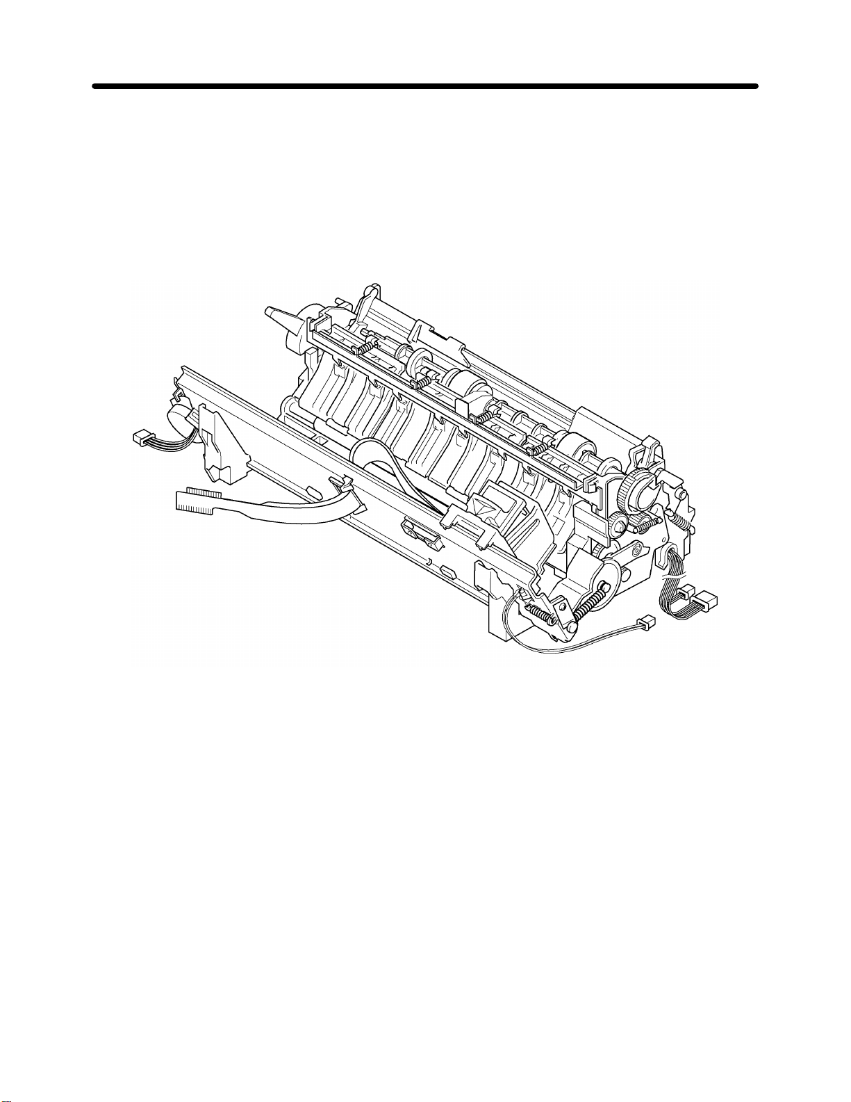
Fig. 1.1 Ink Jet Printer Assembly
1-1
Page 14

THEORY
Mechanical
1.1. Ink Jet Printer System Configuration
The ink jet printer contains the following components:
Carriage assembly
•
Carriage motion control system
•
Paper feed mechanism
•
Maintenance station
•
Sensors
•
The outline of these components are described below.
1. Carriage Assembly
The carriage assembly consists of the carriage and ink cartridge (the cartridge
contains the ink jet nozzles). The carriage consists of the head locker and locker
spring, the rubber pad, and the flat cable.
SERVICE MANUAL
2. Carriage Motion Control System
The carriage motion control system consists of the carriage motor, motor pulley,
timing belt, idle pulley, and the idle pulley holder and holder spring.
3. Paper Feed Mechanism
The paper feed mechanism consists of the paper feed system, paper eject system,
and the paper setting system.
4. Maintenance Station
The maintenance station consists of the MS holder, the MS carriage assembly
(carriage, rubber cap, plunger, compression spring, and extension spring), the wiper,
and the felt form ink absorbers (in spitting trough and under carriage assembly ).
5. Sensors
There are two sensors in the printer assembly: the carriage home position sensor
(attached to the top right end of the CA frame) and the paper end sensor (attached to
the bottom of the PF base at the right rear).
1-2
Page 15
SERVICE MANUAL
THEORY
Mechanical
Fig. 1.2 General View of Printing Mechanism
1-3
Page 16
THEORY
Mechanical
1.2. Ink Jet Operation
1.2.1. Paper Feed Mechanism
The paper feed mechanism consist of the paper feed system, paper eject system, and
the paper setting system.
(1) The paper feed system consists of the ACF shaft gear, separate roller, ACF shaft
locker, locker spring, idle gears 1, 2, 3, and 4, PF roller gear, changer lever 1 and 2,
spring, and the line feed motor.
Paper feed system ACF(Auto cut-sheet feeder)
When the paper feed motor is driven in the opposite direction (reverse rotation) of the
paper feeding, the change lever 1 moves to engage the ACF shaft gear via the idle
gear. The separate roller rotates in the paper separation direction (normal rotation)
and separates a sheet of paper. The separate roller rotates with paper feeding
operation and returns to the initial position. Separated paper is fed to contact PF
roller and the pressure roller by the separate roller where the top of the paper is
registered.
SERVICE MANUAL
Fig. 1.3A Paper Feed Mechanism
1-4
Page 17
SERVICE MANUAL
THEORY
Mechanical
Fig. 1.3B Paper Feed Mechanism
(2) The paper eject system consists of the line feed motor, collar, idle gears 1, 5, and 6,
PF roller gear, eject roller gear, pressure roller, roller holder, holder plate, pressure
roller spring, star wheel holder, and the star wheel.
After paper is registered, the paper feed motor is driven in the paper feeding direction
(normal rotation) and paper is fed by the PF roller and the pressure roller. After
printing paper is ejected by the eject roller and star wheel.
Fig. 1.4 Paper Eject System
1-5
Page 18
THEORY
Mechanical
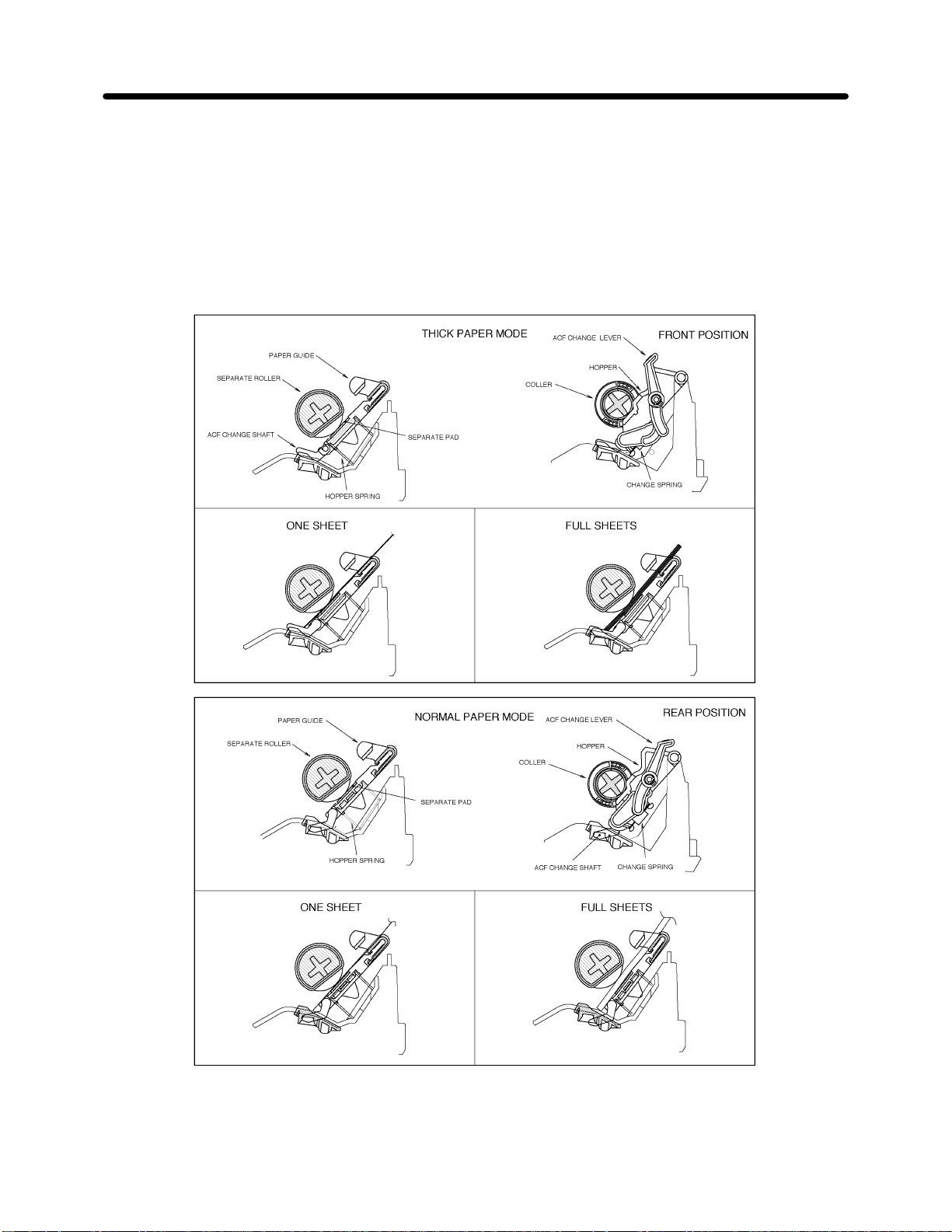
(3) The paper setting system consists of the hopper, hopper spring, separate pad, collar,
SERVICE MANUAL
paper guide, ACF change lever, change spring, and the ACF change shaft.
When inserting a thick paper, the ACF change lever should place at the front
position.
24lb Thick Paper
Envelope
Label
Transparency etc.
Fig. 1.5 Paper Setting System
1-6
Page 19
SERVICE MANUAL
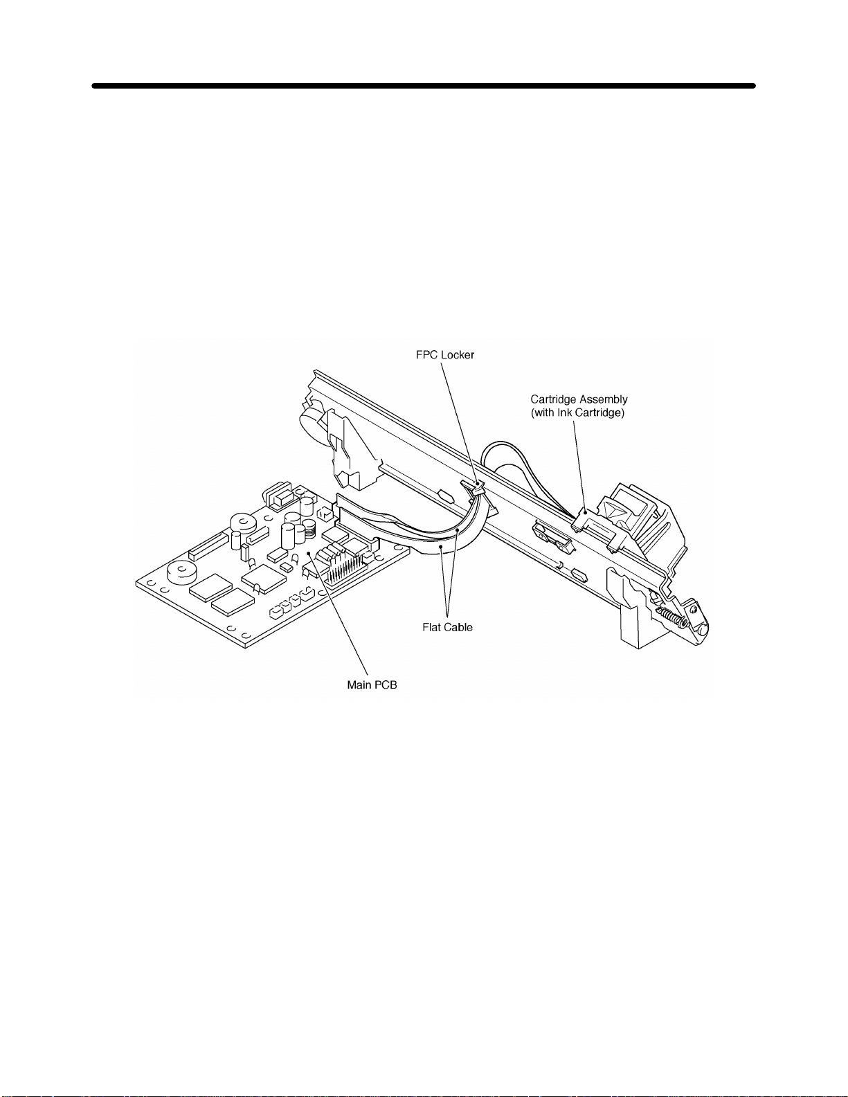
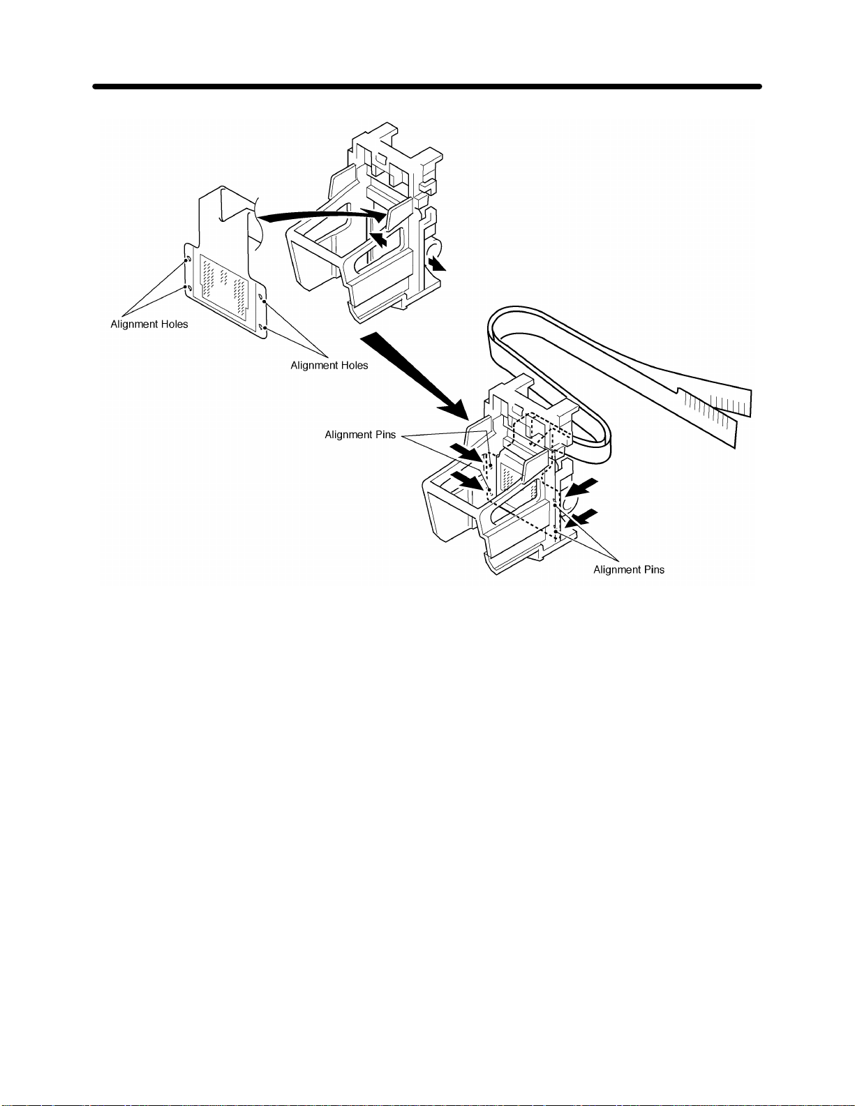
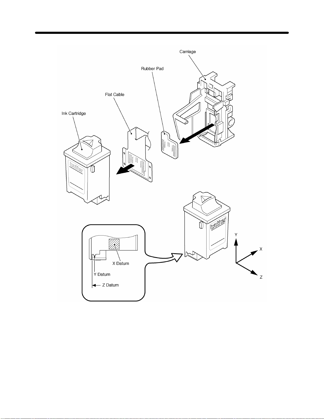
1.2.2. Carriage Assembly
The carriage assembly consists of the carriage and ink cartridge (the cartridge contains
the ink jet nozzles). The carriage consists of the head locker and locker spring, the
rubber pad, and the flat cable. The flat cable connects to the main PCB. See Fig. 1.6.
The printer flat cable must be firmly in contact with the ink jet cartridge for printing to be
enabled. The flat cable is located in the carriage by four alignment pins; proper
alignment of the cartridge to the cable is established in three datums (reference
planes/points): X, Y, and Z. When the cartridge is installed in the carriage, the flat cable
contacts are compressed against the cartridge contacts by the rubber pad. See Figs.
1.7 and 1.8.
THEORY
Mechanical
Fig. 1.6 Printer Flat Cable to Main PCB
1-7
Page 20
THEORY
Mechanical
SERVICE MANUAL
Fig. 1.7 Printer Flat Cable to Cartridge Alignment
1-8
Page 21
SERVICE MANUAL
THEORY
Mechanical
Fig. 1.8 Ink Jet Cartridge to Flat Cable Alignment
1-9
Page 22
THEORY
Mechanical
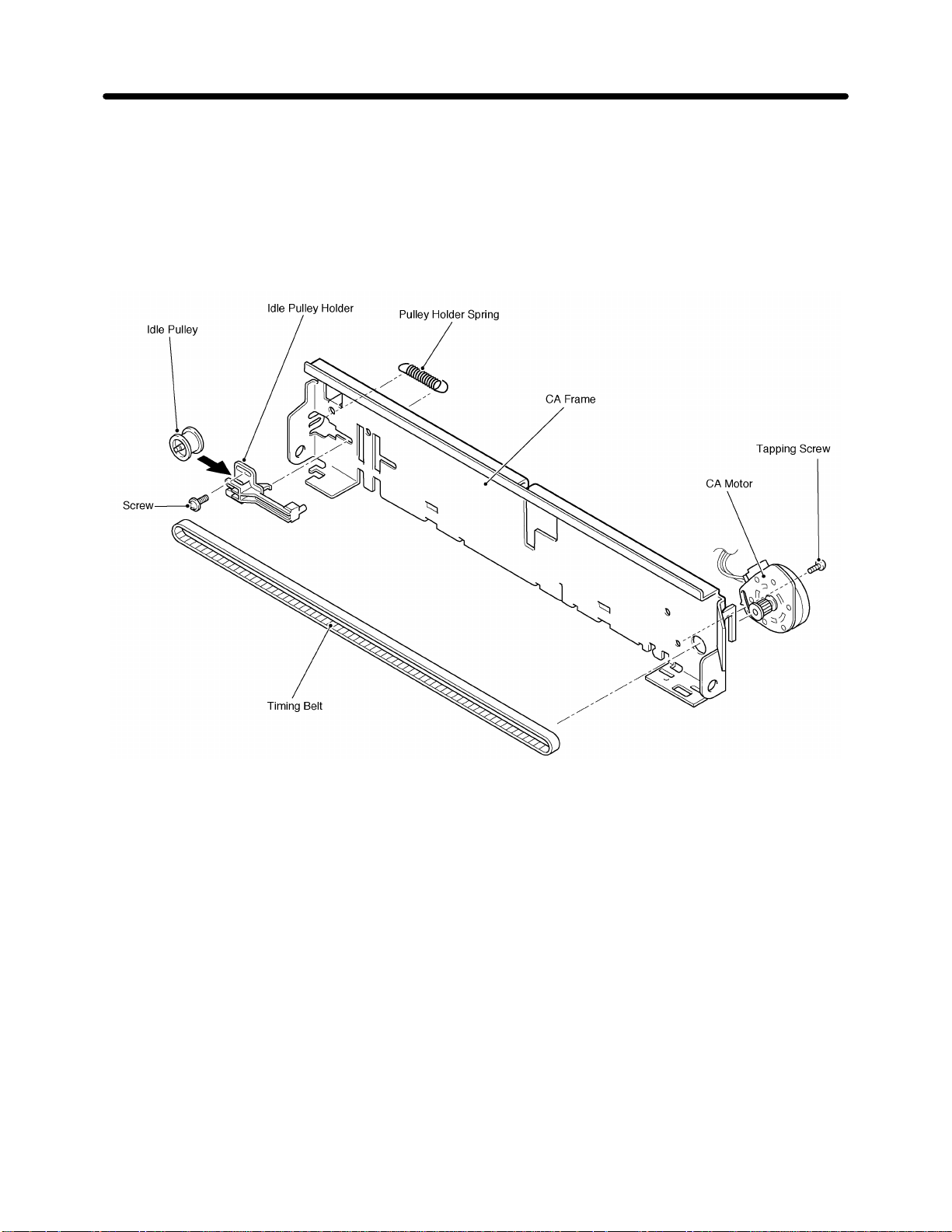
1.2.3. Carriage Motion Control
All operations related to carriage movement are driven by the CA motor. The CA motor
assembly consists of a motor, a timing belt, an idle pulley, and an idle pulley holder and
pulley holder spring: the motor and the idle pulley holder are mounted to the CA frame;
the belt runs between the motor and the pulley. The pulley holder spring between the
idle pulley holder and the CA frame sets belt tension. See Fig. 1.9.
SERVICE MANUAL
Fig. 1.9 Carriage Motion Control
1-10
Page 23
SERVICE MANUAL
1.2.4. Maintenance Station Operation
The maintenance station operation consists of spitting, wiping, capping, and purging.
Table 1.1 shows a summary of maintenance operation for various printer states.
Printer State Spitting Wiping Capping
Power-on 204 2 1
Table 1.1 Summary of Maintenance Operations
THEORY
Mechanical
Beginning of print job 204
(after wiping)
Between pages of continuous
printing
After 6 pages of continuous
printing
After 50 seconds of printing
on the same page
Purging 6,000
Ink cartridge change 204
If no cartridge motion for
more than 30 seconds
Power-off 0 0 0
12 1 0
204
(after wiping)
12
(after wiping)
(after wiping)
(after wiping)
011
10
10
10
11
11
1-11
Page 24
THEORY
Mechanical
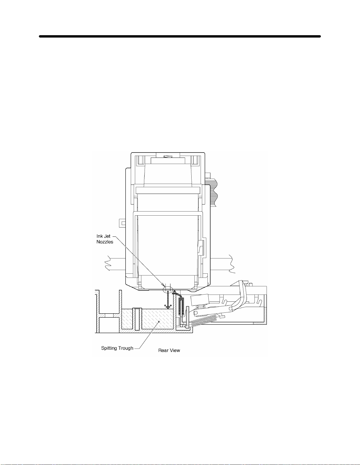
1.2.4.1. Spitting
Spitting is performed at machine power-on, after uncapping from the maintenance
station to clear dormant nozzles, and during the printing process to ensure that
infrequently used nozzles are available when required to print. There must also be
spitting after a wipe cycle, except when the printhead is going to the cap position;
otherwise wiping causes distorted printing if the wiper has experienced any wear.
The trough below he print line is intended to capture the ink during a spit cycle when no
paper is present in the print area. The cup around the wiper is used when spitting is
required and paper is present in the print area. Spitting with paper in print area occurs
when a single page requires longer than 50 seconds to print. All spitting occurs in
trough. At power on, any paper in the print area is ejected.
SERVICE MANUAL
Fig. 1.10 Print Maintenance Operation - Spitting
1-12
Page 25
SERVICE MANUAL
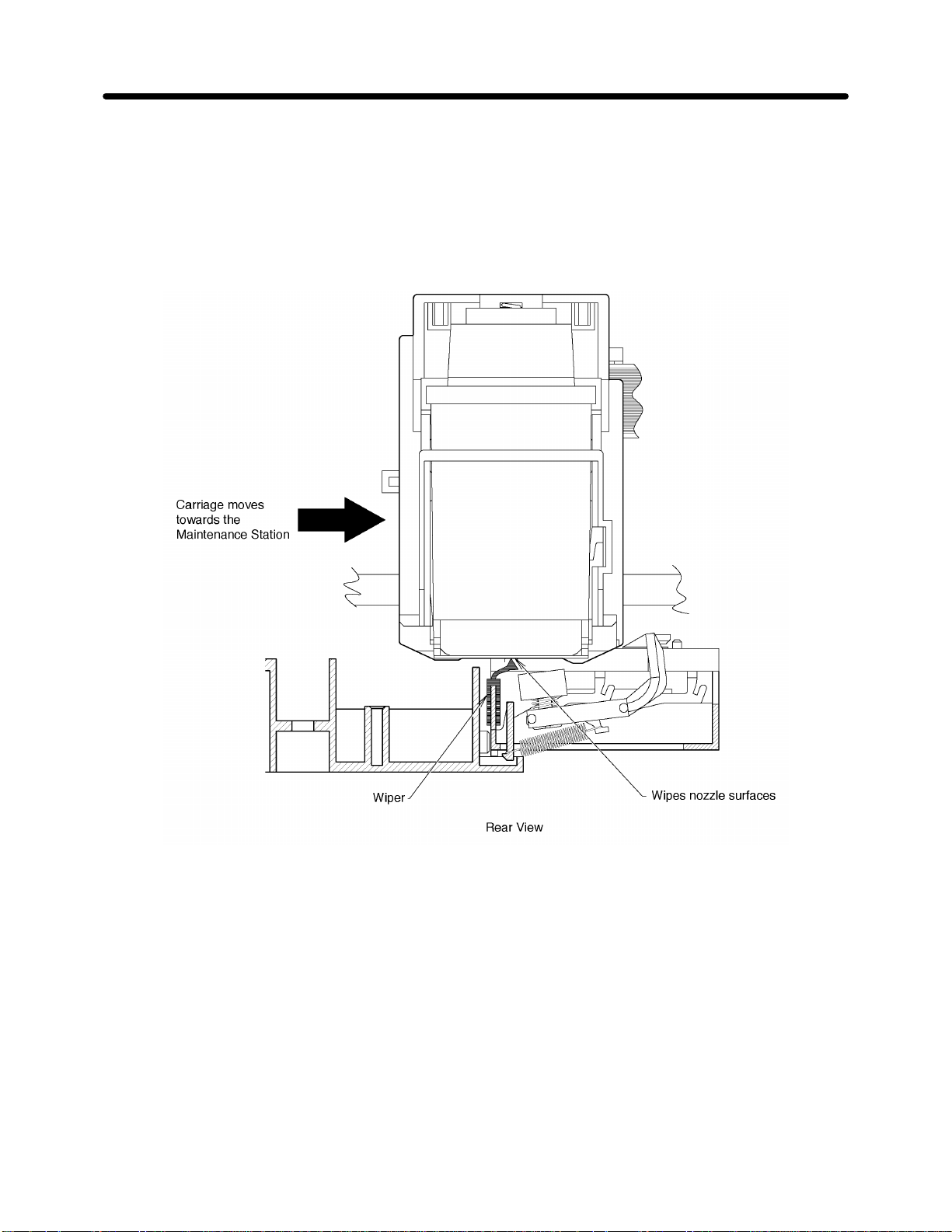
1.2.4.2. Wiping
Wiping of the print head occurs when the cartridge moves across the wiper (in either
direction). The printhead is wiped (twice) when power is turned on, when beginning a
print job (after the print head has been capped for more than four minutes), after six
pages of continuous printing, after 50 seconds of printing on the same page, and after
purging or changing the ink cartridge.
THEORY
Mechanical
Fig. 1.11 Print Maintenance Operation - Wiping
1-13
Page 26
THEORY
Mechanical
1.2.4.3. Capping
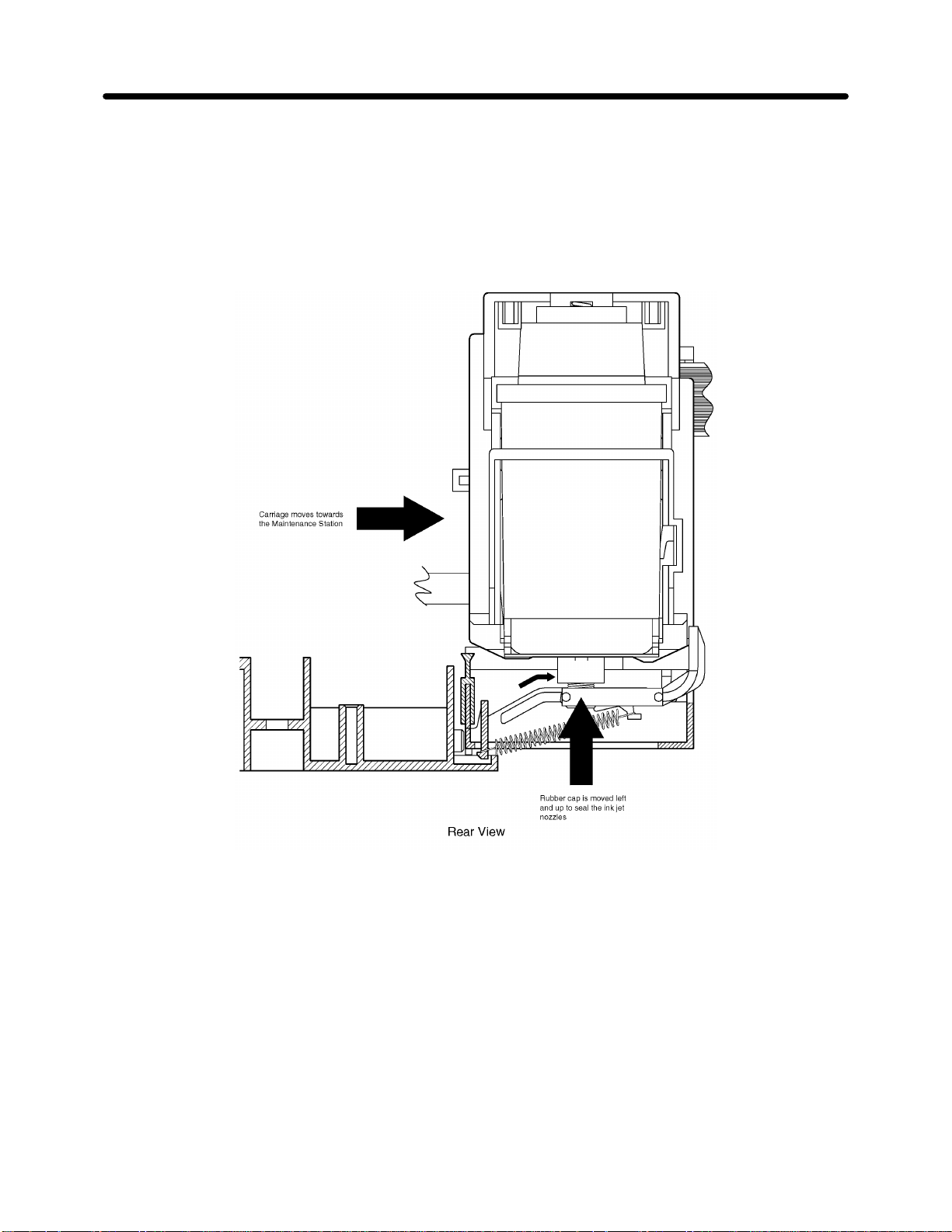
Capping occurs by the movement of the carriage assembly to the maintenance station,
which moves the MS carriage up to the ramp to align the rubber cap with the ink jet
nozzles. The rubber cap prevents the ink from drying and causing the printhead to clog.
The printer will automatically cap the printhead when the system is powered on, when
no data is received for 30 seconds, and after purging or ink cartridge change.
SERVICE MANUAL
1.2.4.4. Purging
The purging function of the maintenance station is a combination of the wipe, cap, and
spit operations. This initiates a sequence of 6,000 spits of each nozzle, in order to clear
clogged ink from the nozzles. The ink is captured in the trough located below the print
line. Purging is user-activated by pressing
keyboard. See 3. "Cleaning the Print head" in Chapter 5, MAINTENANCE, for
instructions.
Fig. 1.12 Print Maintenance Operation - Capping
CODE + SHIFT + INK CHG
1-14
from the
Page 27
SERVICE MANUAL
1.2.5. Sensors
There are two sensors in the printer assembly: the carriage home position sensor (leaf
switch assembly, attached to the right end of the CA frame) and the paper end sensor
(attached to the bottom of the PF base at the right rear).
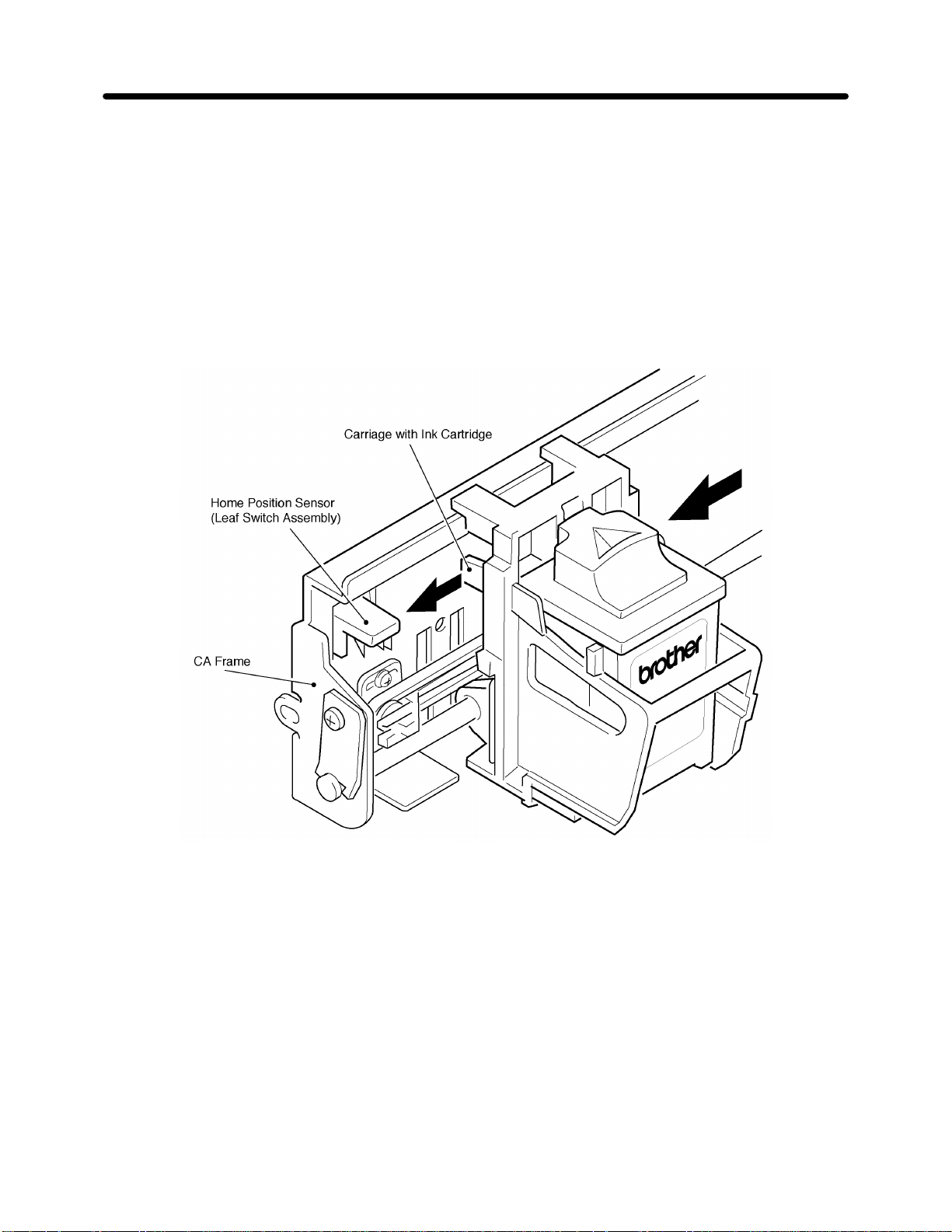
1.2.5.1. Carriage Home Position Sensor
Upon power-up of the system or when the carriage is reset, the carriage moves to the
right end of the printer assembly and activates the home position sensor (leaf switch
assembly). See Fig. 1.13.
THEORY
Mechanical
Fig. 1.13 Carriage Home Position Sensor
1-15
Page 28
THEORY
Mechanical
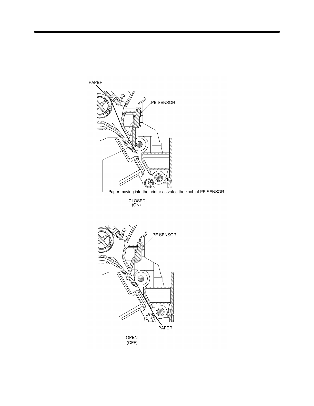
1.2.5.2. PE Sensor
PE sensor detects when the trailing edge of the paper passes the knob of PE sensor.
PE sensor is 1C-1P Switch (normal open.) See Fig. 1.14.
SERVICE MANUAL
Fig. 1.14 PE Sensor Mechanism
1-16
Page 29

SERVICE MANUAL
1.3. INK CHG (Ink Change) Functions
There are two operator-initiated printer maintenance functions available from the
keyboard: ink cartridge replacement and automatic printhead cleaning (purging).
1.3.1. Ink Cartridge Installation/Replacement
There is an ink cartridge installation/replacement function available from the keyboard.
Pressing the key combination
maintenance station to the right end of the printer assembly. Pressing RETURN after
installing or replacing the ink cartridge initializes the system: the cartridge activates the
home position sensor switch and moves the printhead back to the maintenance station.
See Chapter 5, MAINTENANCE, for ink cartridge replacement instructions.
1.3.2. Automatic Print head Cleaning (Purging)
CODE + INK CHG
THEORY
Mechanical
moves the printhead from the
With the ink cartridge installed, pressing the key combination
initiates print head purging. See Chapter 5, MAINTENANCE, for the instructions
CHG
to manually clean the print head.
CODE + SHIFT + INK
1-17
Page 30
THEORY
Mechanical
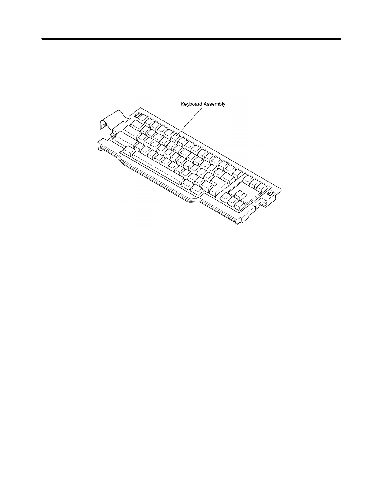
2. Keyboard
The keyboard assembly consists of the keyboard panel and keys, the FPC (flexible
printed circuit) board, and the keyboard base plate.
SERVICE MANUAL
Fig. 1.15 Keyboard Assembly
1-18
Page 31

SERVICE MANUAL
The key tops and key stems are assembled in the keyboard panel. The FPC (flexible
printed circuit) board with rubber contacts is fitted to the base plate. See Fig. 1.16.
The FPC board is a single sheet of film (FPC) on which an electrode pattern is printed in
layers. When the key top is pressed, the key actuator presses the rubber contact; the
conductive part of the contact connects both of the electrodes to output the
predetermined signal for the key.
THEORY
Mechanical
Fig. 1.16 Key Top/Key Stem Assembly
1-19
Page 32

THEORY
Mechanical
3. LCD
The LCD (Liquid Crystal Display) module is secured inside the upper cover by the LCD
bearing at one end and the hinge assembly at the other end so that it can rotate up and
down.
From the closed position, the LCD can be tilted up as much as approximately 132°. The
hinge assembly is the friction type holder that holds the LCD at whatever angle the user
sets within a range approximately 31° from the upright position.
Contrast adjustment varies depending on the model, as indicated below.
<DP-525CJ/LW-800ic, DP-530CJ/LW-810ic, LW-810icBL>
The slide type LCD volume knob located on the right side of the LCD upper cover is
used to adjust the contrast.
<DP-540CJ, DP-550CJ/LW-840ic>
SERVICE MANUAL
The LCD volume located on the left side of the bottom cover is used to adjust the
contrast.
1-20
Page 33

SERVICE MANUAL
THEORY
Mechanical
Fig. 1.17 LCD Unit Installation in the Upper Cover
1-21
Page 34

THEORY
Mechanical
<DP-525CJ/LW-800ic>
SERVICE MANUAL
Fig. 1.18 LCD of DP-525CJ/LW-800ic
1-22
Page 35

SERVICE MANUAL
<DP-530CJ/LW-810ic, LW-810icBL>
THEORY
Mechanical
Fig. 1.19 LCD of DP-530CJ/LW-810ic and LW-810icBL
1-23
Page 36

THEORY
Mechanical
<DP-540CJ, DP-550CJ/LW-840ic>
SERVICE MANUAL
Fig. 1.20 LCD of DP-540CJ, DP-550CJ/LW-840ic
1-24
Page 37

SERVICE MANUAL
CHAPTER 2 ELECTRICAL THEORY
1. System Configuration
The major electronic component parts of the machine are shown in Fig. 2.1.
1.1. Main PCB (Printed Circuit Board)
The main PCB controls the entire system including the LCD, ink cartridge, and the
motors in the printer.
The motors and the ink cartridge are driven by +24 VDC, and the CPU and other
devices are driven by +5 VDC.
1.2. Switch PCB (Printed Circuit Board)
Receiving power from the AC adaptor, the switch PCB supplies voltage to the main
PCB, through the power switch and the fuse.
THEORY
Electrical
1.3. Keyboard FPC (Flexible Printed Circuit)
The keyboard FPC has electrodes arranged in a matrix circuit pattern. The keyboard
status is sent from the FPC to the main PCB.
1.4. FDD (Floppy Disk Drive) Module
The FDD can read and write information supplied to the main PCB. The FDD is driven
by +5 VDC.
1.5. LCD (Liquid Crystal Display) Module
The LCD PCB contains the driver for the dot matrix of the LCD on which various
information is displayed. The CFL backlight (Models: DP-550, LW-810icBL, and LW840ic) is driven by +5 VDC from the main PCB.
2-1
Page 38

THEORY
Electrical
SERVICE MANUAL
Fig. 2.1 Major Electronic Component Parts
2-2
Page 39

SERVICE MANUAL
2. Ink Jet Printer Configuration
The following describes the operation of the ink cartridge, motors and other
components.
2.1. Ink Cartridge
An ink cartridge contains both ink and the print head which has 56 nozzles and prints at
a resolution of 300 dpi.
2.2. Carriage Motor
The carriage step motor drives the carriage right and left with precision motion control.
2.3. Line Feed Motor
The line feed motor feeds the paper forward and in reverse.
THEORY
Electrical
2.4. Carriage Home Position Sensor
The carriage home position sensor is mounted on the right of the CA frame. It detects
the carriage home position to synchronize the carriage position and motor phase.
2.5. PE (Paper End) Sensor
The PE sensor detects whether or not paper is in the printer. The PE sensor is located
at the right rear of the bottom of the PF base.
2-3
Page 40

THEORY
Electrical
3. Power Supply Circuit
3.1. Configuration
Fig. 2.2 shows the power supply circuit.
The power supply section converts the unstable input (PWR) supplied from the switch
PCB into stable +24 VDC (for motors and print head) and +5 VDC (for logic).
A 2-channel switching regulator IC (#4) converts unstable input into stable output.
SERVICE MANUAL
Fig. 2.2 Power Supply Circuit
2-4
Page 41

SERVICE MANUAL
3.2. +24V Generator
The timing chart of the +24V generation circuit during idling is shown in Fig. 2.3.
Switching Q6 by #4 at 100 kHz boosts the input to a stable +24V.
Energy is accumulated in L1 while Q6 is ON and the power is transmitted to the output
side by the back electromotive force generated from the moment Q6 is turned OFF.
Stabilization to +24V is achieved by changing the ON-OFF duty ratio of Q6.
THEORY
Electrical
3.3. +5V Generator
The timing chart of the +5V generation circuit during idling is shown in Fig. 2.4.
Switching Q12 by #4 at 100 kHz reduces the input voltage to a stable +5V.
While Q12 is ON, energy is supplied to L3, C31, and load. The energy accumulated in
L3 is supplied to load through D2. Stabilization to +5V is achieved by changing the ONOFF duty ratio of Q6.
Fig. 2.3 Timing Chart of +24V Generation Circuit
Fig. 2.4 Timing Chart of +5V Generation Circuit
2-5
Page 42

THEORY
Electrical
4. Reset Circuit
4.1. Configuration
The reset circuit is shown in Fig. 2.5. The reset signal (MRST) used to initialize the
system is generated using the leading and trailing edges of the +5V voltage.
The reset signal is input to the following devices.
SERVICE MANUAL
Device Pin
CBIC (#8) 17
Printer drivers (#2, #3) 5
Fig. 2.5 Reset Circuit
2-6
Page 43

SERVICE MANUAL
5. CBIC and Peripherals
5.1. CBIC #8
CBIC (#8) is a Cell-based IC in which logic circuits for controlling peripherals are
integrated with the CPU core. With the functions incorporated in it, CBIC (#8) controls
all the functions of the system including printer control and control of the LCD display.
5.2. Main ROM (#11, #12)
Installation of a maximum of 8 Mbytes (32 Mbits x 2 pcs.) of ROM is possible. The
capacity of ROM installed in the machine is determined by whether or not the chip
resistor R71 is installed.
R71 installed: 32 Mbit ROM
R71 not installed: 16 Mbit ROM
THEORY
Electrical
5.3. Main RAM (#9, #10)
The following RAM can be installed at #9 and #10.
#9: 16 Mbit DRAM
#10: 4 Mbit DRAM
Note that simultaneous installation of RAM at #9 and #10 is not allowed.
5.4. Video RAM (#6)
The capacity of the video RAM used to retain the data to be displayed on the LCD is
256 Kbit. It secures the display area for different sizes of LCDs, from 480 x 64 dots to
640 x 400 dots.
The RAM area not necessary for the LCD display can be used as the work area.
5.5. Printer Driver Circuits (#2, #3, Q1 to Q4, and Q23 to Q26)
The printer driver circuits convert the motor phase driver signals output from CBIC (#8)
to +24V drive signals, which are output to the motors and ink cartridge.
5.6. FDC (Floppy Disk Controller)
The FDC controls floppy disk drive access through the FDD drive circuit.
2-7
Page 44

THEORY
Electrical
5.7. Clock Circuit
Four different clock circuits shown in Table 2.1 are incorporated in the main PCB.
SERVICE MANUAL
Table 2.1 Clock Circuit
Clock Circuit Frequency Function
16MHz XT2 is the standard
clock for FDD control;
it inputs for #5 (pins
25, 26).
18MHz XT1 is the standard
clock for FDD control;
it inputs for #8 (pin
167).
5.8. Buzzer Drive Circuit
The buzzer drive circuit is shown in Fig. 2.6. A 4 kHz pulse of 50% duty is output from
port BUZ (pin 25) of CBIC (#8) when buzzer operation is needed.
The piezoelectric element in BZ1 generates sound on reception of this pulse. The
output from port BUZ is Hi-Z when the buzzer is not in operation.
20MHz XT3 is the standard
clock for printer control
and other several
timing; it inputs for #8
(pints 14, 15).
14.74MHz XT4 is the standard
clock for CPU core; it
inputs for #8 (pints 94,
95).
Fig. 2.6 Buzzer Drive Circuit
2-8
Page 45

SERVICE MANUAL
5.9. Country Specification Change-over
The country specification change-over circuit is shown in Fig. 2.7. The country
specification is recognized by the CPU by sensing solder on the solder points.
THEORY
Electrical
Fig. 2.7 Country & Model Specification Change-over Circuit
2-9
Page 46

THEORY
Electrical
5.10. RS-232C I/F Circuit
The RS-232C I/F circuit is shown in Fig. 2.8. The driver IC (#1) converts the signal level
(+5V – ±0V) on the main PCB to the RS-232C signal level in the external line and vice
versa.
SERVICE MANUAL
Fig. 2.8 RS-232C I/F Circuit
2-10
Page 47

SERVICE MANUAL
6. Printer Control
6.1. Ink Jet Head Control
The ink jet head drive circuit is shown in Fig. 2.9. The ink jet head has 50 active
nozzles (monochrome). Two addressable multiplexing printer drive circuits (#2, #3)
activate the nozzles for printing. Custom circuitry controls the timing and
synchronization of ink deposited as the cartridge moves across the paper in printing.
The same system controls ink jet head maintenance (spitting into the trough).
THEORY
Electrical
Fig. 2.9 Ink Jet Head Drive Circuit
2-11
Page 48

THEORY
Electrical
6.2. Carriage Motor Control
The carriage motor control circuit is shown in Fig. 2.10. +24 VDC is supplied to the
motor through connector CN3, pin 5. Motor phases A, B, C, and D are driven by the
CBIC (#8) through pins 150 - 153, respectively. The outputs of the CBIC turn darlington
transistors Q1 - Q4 on and off, which in turn affect the motor phases.
SERVICE MANUAL
Fig. 2.10 Carriage Motor Drive Circuit
2-12
Page 49

SERVICE MANUAL
6.3. Line Feed Motor Control
The line feed motor drive circuit is shown in Fig. 2.11. The line feed motor is powered
by +24 VDC. Each of he four phases of the motor is excited when CBIC (#8), via ports
LF-A, B, C, and D, outputs to turn on the darlington transistors Q23 - Q26.
This provides a path to ground through the transistor, which allows current to flow.
When the printer gate array outputs a LOW, the transistor remains off.
THEORY
Electrical
Fig. 2.11 Line Feed Motor Drive Circuit
2-13
Page 50

THEORY
Electrical
6.4. Carriage Home Position Sensor
The carriage home position sensor circuit is shown in Fig. 2.12. The HIGH/LOW status
of the sensor is read by pin 164 of the CBIC (#8). The signal goes LOW when the
carriage reaches the home position.
Fig. 2.12 Carriage Home Position Sensor Circuit
6.5. PE Sensor
The PE sensor detection circuit is shown in Fig. 2.13. The HIGH/LOW status of the PE
sensor is read by pin 165 of the CBIC (#8). The signal is HIGH if there is no paper at
the sensor position.
SERVICE MANUAL
Fig. 2.13 PE Sensor Detection Circuit
2-14
Page 51

SERVICE MANUAL
7. Switch PCB
7.1. Configuration
The Switch PCB is installed between the AC adaptor and the main PCB to turn the
power on and off and protect devices at the occurrence of an alarm, etc.
Fig. 2.14 shows the external view of the switch PCB and Fig. 2.15 the switch PCB
circuit.
THEORY
Electrical
Fig. 2.14 External View of the Switch PCB
Fig. 2.15 Switch PCB Circuit
2-15
Page 52

THEORY
Electrical
8. Keyboard System
8.1. FPC Operation
The keyboard is a flexible printed circuit (FPC) board on which the circuit pattern and
electrodes are printed. When a key is pressed, the key stem is forced down until the
carbon-type conductive silicone rubber makes a contact with the FPC electrode and
electricity is conducted. See Fig. 2.16.
SERVICE MANUAL
Key Actuator
Contact Rubber
Carbon Electrodes
Carbon Silicon Conductive Rubber
FPC Board
Base Plate
Fig. 2.16 Key/FPC Operation
2-16
Page 53

SERVICE MANUAL
8.2. Keyboard Scan
Fig. 2.17 shows the pattern from wiring electrodes on the board (this figure shows only
simplified wiring for ease of explanation and is slightly different from the actual wiring).
Refer to Fig. 2.17 to understand the keyboard scanning operation described. When a
key is not pressed, continuity does not exist in any combination of the matrix (e.g. X1
and Y1 or X2 and Y2). For example, if key [A] is pressed, continuity will exist only in X2
and Y3, but not between any other pairs of points which are left in the OFF status. In
other words, if continuity exists between X2 and Y3, it means that key [A] is being
pressed.
THEORY
Pattern Circuit
Pattern Circuit
Electrical
Fig. 2.17 Electrode Wiring
2-17
Page 54

THEORY
Electrical
8.3. Keyboard Control Circuit
The keyboard control circuit is shown in Fig. 2.18.
The matrix pattern on the keyboard FPC controls port 7 (0:7) of CBIC (#8) according to
data signals KO0 through KO8. The LOW level signals are output to output lines KO0
through KO8. The electrode wiring is scanned line by line. The result of scanning is
input to P70 through P77 of CBIC (#8). CBIC (#8) detects which key has been pressed.
The key matrix given in Fig. 2.19 corresponds to the key arrangement shown in Fig.
2.20.
SERVICE MANUAL
Fig. 2.18 Keyboard Control Circuit
2-18
Page 55

SERVICE MANUAL
THEORY
Fig. 2.19 Keyboard Matrix
Electrical
Fig. 2.20 Keyboard Symbols (Corresponding to Keyboard Matrix in Fig. 2.19)
2-19
Page 56

THEORY
Electrical
9. LCD Module
The block diagram of the LCD display operation is shown in Fig. 2.21. CBIC (#8) on the
main PCB outputs the LCD module control signals to the LCD module. The LCD drive
voltage (VEE) is generated by DC-DC convertor by the pulses output from CBIC (#8).
Display data, the data written to the SRAM (#6) that functions as Video RAM is always
sent to the LCD module as 4-bit parallel data.
SERVICE MANUAL
Fig. 2.21 LCD Display Operation Block Diagram
2-20
Page 57

SERVICE MANUAL
9.1. LCD Control
The CBIC (#8) controls the LCD control signals and the SRAM access.
The display data written to the SRAM (#6) is read by the CBIC (#8) in regular intervals,
converted into the 4-bit parallel data by the CBIC (#8) and then sent to the LCD module.
Black and white of the display data are inverted by connecting the R55 (#8 REV
terminal). Connect the R55 if the transmission type LCD is used.
The timing of display control signals differs according to the LCD type. The timing is set
by the status of the DMODE (3:0) terminal in the CIBC (#8) in the reset state and by the
setting in the program after the reset is canceled. An example of the control signal
timing chart is shown in Fig. 2.22.
THEORY
Electrical
Fig. 2.22 Example of Control Signal Timing Chart
9.2. LCD Module
The LCD modules used in the respective models are shown in Table 2.2. The control
signal timing and drive voltage (VEE) differ according to the LCD module.
Table 2.2 Table of LCD Modules
Specification No. of Horizontal
Model Name
DP-525CJ LW-800ic 480 64 Reflective no –17.5 to –14.5
DP-530CJ LW-810ic 480 128 Reflective no –17.5 to –14.5
LW-810icBL 480 128 Transflective yes –17.5 to –14.5
DP-540CJ 640 400 Reflective no +22 to +30
DP-550CJ LW-840ic 640 400 Transmissiveyes +26 to +37
Dots
Note: VEE voltage is the values measured at connectors CN7 and CN8.
No. of
Vertical Dots
Panel Type Backlight VEE (V)
2-21
Page 58

THEORY
Electrical
9.3. LCD Drive Voltage (VEE) Generation Circuit
The polarity of the LCD drive voltage (VEE) differs according to the LCD module.
Fig. 2.23 shows the circuit for the LCD module driven by the minus VEE voltage. The
+5 VDC source voltage is switched continuously by the 20 kHz pulses from CBIC (#8) to
energize L5. The reverse voltage generated by L5 is rectified by D6 and regulated by
ZD5. The ZD5 determines the VEE voltage (about -16 V).
The LCD module driven by the plus VEE voltage uses the circuit shown in Fig. 2.24.
The +24 VDC source voltage is switched continuously by the 90 kHz pulses from CBIC
(#8) to energize L2. The voltage generated by L2 is rectified by D5 and regulated by
ZD4 and ZD6. The ZD4 and ZD6 determine the VEE voltage.
VEE voltage is adjusted by turning VR1.
SERVICE MANUAL
Fig. 2.23 LCD Drive Voltage Generation Circuit (Minus Voltage VEE)
Fig. 2.24 LCD Drive Voltage Generation Circuit (Plus Voltage VEE)
2-22
Page 59

SERVICE MANUAL
9.4. Power Supply for CFL Backlight
The CFL backlight circuit consists of the control circuit that turns ON/OFF the CFL and
the inverter PCB.
The ON/OFF status of the CFL is controlled by the CFLON terminal of the CBIC (#8).
The inverter PCB converts +5V to AC voltage to drive the CFL tube. The type of
inverter PCB differs according to the LCD.
Fig. 2.25 shows the CFL backlight circuit.
THEORY
Electrical
Fig.2.25 CFL Backlight Circuit
2-23
Page 60

THEORY
Electrical
10. FDD (Floppy Disk Drive) Control
10.1. FDD Configuration
The FDD consists of two sections: the FDD controller and the FDD module. The FDD
controller circuit controls the contents to be received and stores the data in the FDD
module. The FDD module drives the motors, sensors, and magnetic head. The
interface signals between the FDD and the FDC are shown in Table below:
Table.2.3 FDC(#5) and FDD Module Links (Interface Signals)
Signals Pin No. Function
Read/Write
Circuits
Motor Drive
Circuit
Status Check WRITE PROTECT 28
DRIVE SELECT Ø 10 12
WRITE GATE 24
WRITE DATA 22
READ DATA 30
SIDE1 SELECT 32
DC
MOTOR
STEP
MOTOR
16
ON
STEP 20
MOTOR
DIRECTION
SELECT
18
INDEX 8
TRACKØØ 26
DISK CHANGE 34
SERVICE MANUAL
This signal is set to LOW when the FDD unit is
opening (except for the DC Motor).
When this signal is set to LOW, data can be written
by the WRITE DATA signal. When this signal is set
to HIGH, the READ and STEP operations are
enabled.
Data is written at the falling edge of this signal while
the WRITE GATE signal is LOW.
This signal indicates the polarity data read by the
head.
This signal is used to select the head:
LOW: Head 1
HIGH: Head 0
This signal becomes LOW, starting the DC motor,
when a disk is set in the drive. Setting this signal to
HIGH or removing the disk stops the DC Motor.
This signal sets the head in the direction designated
by the DIRECTION signal.
This signal designates the movement of the
read/write head:
LOW: Inward to the disk's center
HIGH: Outward from the disk's center.
When this signal is LOW, either there is no disk in
the drive or the disk in the drive is write-protected.
This signal indicates the beginning of a track by
outputting one pulse in each rotation of the disk.
When this signal is LOW, the head is located at track
00 (the outside track).
Otherwise, the signal is HIGH.
When this signal is LOW, there is no disk in the drive.
2-24
Page 61

SERVICE MANUAL
10.2. FDD Operation
10.2.1. Basic Operation
CBIC(#8) writes commands to FDC(#5), and the FDC(#5) controls the FDD in
accordance with these commands and reads/writes data.
See Fig. 2.26.
10.2.2. Interface between CBIC (#8) and FDC (#5)
If CBIC(#8) accesses an internal register other than the data resister in FDC (#5), the
normal read/write operation will be performed.
If CBIC(#8)transmits data to or receives data from FDC (#5), DMA communications will
be performed using the DMA function of CBIC(#8).
CBIC(#8) resets FDC(#5),detects the density signal which indicates whether the floppy
disk is a 2DD or 2HD, and output to FDC(#5).
THEORY
Electrical
Fig.2.26 FDD Block Diagram
2-25
Page 62

THEORY
Electrical
10.3. FDD Module
The FDD Module is composed of the motor, sensor, magnetic head, and the IC that
drives them. The FDD Module is controlled by the FDC (#5) of the MAIN PCB.
10.3.1. Read/Write Circuit
In read operation, the circuit amplifies the analog signals picked up by the magnetic
head and converts the analog signal to serial digital pulses. The serial pulses are then
transmitted to the FDC (#5) and decoded to parallel digital data.
In write operation, the circuit controls the current at the magnetic head according to the
serial digital pulses from the FDC #5.
10.3.2. Motor Drive Circuit
The motor drive circuit consists of two parts: a DC motor drive circuit and a stepping
motor drive circuit.
The DC motor drive circuit controls the DC motor, which rotates the spindle according to
the MOTOR ON signal from the FDC. The stepping motor drive circuit controls the
stepping motor, which operates the magnetic head unit according to the "STEP" and
"DIRECTION SELECT" signals from the FDC #5.
SERVICE MANUAL
10.3.3. Sensor Circuits
The following sensor circuits detect the status of the FDD:
1. Write Protect Sensor
When a write-protect notch on a disk is set to the write-protect position, the "WRITE
PROTECT" signal becomes LOW. A micro-switch is used for detection.
2. Index Sensor
The "INDEX" signal shows the beginning of a track; when the beginning of a track is
detected, the "INDEX" signal becomes LOW. A magnetic sensor is used for
detection.
3. Track00 Sensor
When the magnetic head is positioned in track 0 on a disk, the "TRACK 00" signal
becomes LOW. A photo sensor is used for detection.
2-26
Page 63

SERVICE MANUAL
4. Disk-in Sensor
When a disk is inserted in the FDD, this sensor outputs a LOW level signal (HIGH
when no disk).
The output of the sensor is connected to the controller and sent as a "DISK
CHANGE" signal that shows whether a disk is changed; when a disk is changed, the
"DISKCHANGE" signal becomes LOW.
Once the "DISK CHANGE" signal becomes LOW, it remains low until the "STEP"
signal is received from the FDC #5.
THEORY
Electrical
2-27
Page 64

REPAIR
SERVICE MANUAL
PART II REPAIR
CHAPTER 3 TROUBLESHOOTING
1. Introduction
This chapter explains troubleshooting procedures for the word processor. Since it is
impossible to troubleshoot all instances of a problem, only a limited number of cases
are presented. Thorough understanding of the procedures given in each section is
essential for efficient troubleshooting, and can provide a good insight to the problem.
2. Precautions
2.1. Personal Safety
Troubleshooting
WARNING:
In addition to any specific warnings as described above, be sure to take the following
precautions for your personal safety:
• Unplug the AC adapter from the AC outlet before removing the covers and PCBs, or
before making any mechanical adjustments.
• Unplug the AC adapter from the AC outlet before checking continuity.
• When disconnecting a connector, grasp it firmly. Do not pull on the connector's lead
wires. If the connector has a lock mechanism, unlock it before trying to disconnect it.
If there is chance of electrical shock, this symbol will precede any
instructions in this manual. Follow the safety advice carefully!
2.2. Handling ESD-Sensitive Parts
Many electronic products use parts that are known to be sensitive to electrostatic
discharge (ESD). To prevent damage to ESD-sensitive parts, observe the caution
symbols throughout these instructions, as well as the additional precautions below.
3-1
Page 65

Troubleshooting
REPAIR
SERVICE MANUAL
CAUTION:
In addition to the usual precautions, such as turning off power before removing circuit
boards:
Keep the ESD-sensitive part in its original shipping container (a special "ESD bag")
•
until you are ready to install it.
Do not place the ESD-sensitive part on the machine cover or on a metal table; if you
•
need to put down the ESD-sensitive part for any reason, first put it into its special bag.
When holding ESD-sensitive parts, limit your body movement to prevent an increase
•
of static electricity from clothing fibers, and furniture.
Hold the ESD-sensitive part by its edge connector shroud (cover); do not touch its
•
pins. If you are removing a plugable module, use the correct tool.
Be extra careful in working with ESD-sensitive parts when cold-weather heating is
•
used, because low humidity increases static electricity.
Electrostatic Discharge Hazard
Wear an anti-static wrist strap with ground wire to prevent damage to
sensitive electronic components.
Prevent ESD-sensitive parts from being accidentally touched by other personnel.
•
Install machine covers when you are not working on the machine, and do not put
unprotected ESD-sensitive parts on a table.
If possible, keep all ESD-sensitive replacement parts stored in a grounded metal
•
cabinet (case) until ready for use.
3. Checks Before Repair
CAUTION:
Check the following possible causes before attempting more extensive repairs to the
machine:
Electrostatic Discharge Hazard
Wear an anti-static wrist strap with ground wire to prevent damage to
sensitive electronic components.
3-2
Page 66

REPAIR
SERVICE MANUAL
Run the appropriate Self Test operation (from the software) for the suspected problem
•
before attempting any mechanical or electrical troubleshooting.
Supply voltage: Check the AC input voltage and DC supply voltage for all sections.
•
Make sure they meet specified voltage values.
Connectors: Check all connectors and make sure they are tight.
•
Fuses: Check for blown fuses (F1 and the thermo-fuse inside the AC adapter).
•
NOTE:
In the logic control circuit, it is difficult to isolate faulty points in areas connected tot he
•
CPU by the address bus or the data bus. If a suspected problem involves the address
bus or data bus, first check the solder bridge and the cut circuit pattern. If a faulty point
cannot be isolated, replace the peripheral devices or the PCB.
4. Checks After Repair
After completing a repair, check to confirm that the trouble has been eliminated. Also,
record the troubleshooting procedures used for reference.
Troubleshooting
3-3
Page 67

Troubleshooting
5. Troubleshooting Flow Charts
Power ON
REPAIR
SERVICE MANUAL
LCD operating
correctly?
YES
Carriage (print head)
moves?
YES
Printer home position
detected?
YES
Keys work properly?
YES
Prints normally?
NO
NO
NO
NO
NO
Problem No. 1
Problem No. 2
Problem No. 3
Problem No. 4
Problem No. 5
YES
Line Feed operates
Paper feeds normally?
correctly?
YES
A
Fig. 3.1 Troubleshooti ng Fl owchart
NO
Problem No. 6
3-4
Page 68

REPAIR
SERVICE MANUAL
Troubleshooting
A
Does the buzzer sound
when an invalid key is
pressed?
YES
Does the LCD operate?
YES
Does the LCD display
correctly?
YES
Does the unit print
when paper is set, or print when
no paper is set?
YES
Does the FDD operate
correctly?
NO
NO
NO
NO
NO
Problem No. 7
Problem No. 8
Problem No. 9
Problem No. 10
Problem No. 11
YES
Does the
fax/modem (optional)
Line Feed operates
operate properly?
correctly?
NO
Problem No. 12
YES
Does an error message
appear on the display?
YES
Problem No. 13
NO
END
Fig. 3.2 Troubleshooti ng Fl ow char t ( cont inued)
3-5
Page 69

Troubleshooting
SERVICE MANUAL
6. Failure Analysis
The following table lists the failure problems for troubleshooting all basic systems. See
the Troubleshooting Tables on the following pages for a troubleshooting protocol.
Table 3.1 Failure Analysis
No Problem
1 Nothing happens when the power is switched on (Nothing appears on the LCD).
2 When the power is switched on, the LCD display operates but the carrier does not
return to its home position.
3 When the power is switched on, the carrier moves to the right but cannot detect
its home position (i.e., the home position indexing mechanism is faulty).
4 Keys malfunction (do not insert characters or insert wrong characters)
5 Printing results abnormal (various unsatisfactory printing results)
6 The line feed (LF) motor does not rotate normally.
REPAIR
7 The buzzer does not sound.
8 Power in on, but nothing appears on the LCD.
9 LCD displays operates, but data displayed is incorrect (does not match input).
10 Word Processor prints when no paper is set, or will not print when paper is set
(Paper End Sensor malfunction).
11 The FDD does not operate correctly.
12 Communication function (optional fax/modem) does not work or does not work
properly.
13 An error message appears on the display.
3-6
Page 70

REPAIR
SERVICE MANUAL
Troubleshooting Tables
Troubleshooting
1
Problem:
Points to Check Probable Cause Corrective Action Repair
Is (at least) about +16 V present on
the output plug if the AC adapter?
Is fuse F1 on the Switch PCB OK? Blown fuse Replace the Fuse.
Are harnesses CN1 on the Switch
PCB properly connected?
Is about +16V present at CN1 on the
Switch PCB?
Is +5V present on the Main PCB? Defective ZD7 or Q12
Problem:
2
Points to Check Probable Cause Corrective Action Repair
With motor cable disconnected, is
+24 V present at CN3, pin 5 on the
Main PCB?
Is resistance value across each of
the phases and COM terminal (pin
5) of the carriage motor correct?
(about 45Ω) Phases → ;(5-1); B(5-
2); ‚b(5-3); D(5-4)
Are carriage motor drive pulse
output from pin 150-153 of #8 just
after power is switched on ? (Use
an oscilloscope.)
Is output at the pin of transistors Q1Q4 on and off according the drive
pulses indicated above?
Does the carriage motor
occasionally stall?
Nothing happens when the power is switched on (nothing appears on the LCD).
Defective AC adapter Replace the AC
adapter.
Harnesses improperly
connected.
Defective Switch PCB Replace the Switch
(Main PCB)
When the power is switched on, the LCD display operates but the carrier does not
return to its home position.
Defective Q6 (Main
PCB)
Broken wire in the
carriage motor
assembly (broken wire
in the carriage motor)
(defective connector)
Defective #8 (Main
PCB)
Defective transistor
Q1-Q4 or circuit on the
Main PCB
Incorrect motor phase
at home position (start
up).
Replace the Switch
PCB.
PCB.
Replace the Main
PCB.
Replace the Main
PCB
Replace carriage
motor assembly.
Replace the Main
PCB.
Replace the Main
PCB.
Adjust motor phase at
home position (see
Chapter 4 "INK JET
PRINTER
ASSEMBLY").
Rework the
connectors.
Replace ZD7,
Q12.
Replace Q6.
Replace #8.
Replace Q1Q4.
Problem:
3
Points to Check Probable Cause Corrective Action Repair
Is the carriage index (home position)
switch open?
When the power is switched on, the carrier moves to the right but cannot detect its
home position.
CA index switch is not
adjusted correctly.
3-7
Readjust.
Page 71

Troubleshooting
Points to Check Probable Cause Corrective Action Repair
Does the signal level at pin 1 of
CN13 remain HIGH when the
carriage index switch is closed?
Is the carriage index switch
connected to CN13?
Broken wire in the
carriage index switch
assembly
Incorrect connection Reconnect.
Replace the carriage
index switch assembly
(after confirming
discontinuity).
REPAIR
SERVICE MANUAL
4
Problem:
Points to Check Probable Cause Corrective Action Repair
Is the key top and the key actuator
correctly mounted?
Is the keyboard FPC securely
connected to Main PCB CN12?
When a bad key is pressed, does
the matrix row in which the pressed
key is connected go LOW in
synchronization with the output
timing of output drive #8?
Is solder present at the correct
country specification change-over
solder point?
5
Problem:
Keys malfunction (do not insert characters or insert wrong characters)
[Abnormal Printing]
• Voids in characters • Light print • Prints off the page
• Prints satellites • Carrier moves, but does not print
• Print head dries out prematurely • Vertical alignment off
• Ink smearing • Vertical streaks on paper
• Print lines crowded • Gaps or overlapped areas in print
• Will not print in color • Colors will not print correctly.
Faulty keyboard
assembly
Keyboard PCB not
connected properly.
If YES, faulty Main
PCB.
If NO, faulty keyboard.
Incorrect or faulty
solder point for
specified country
(language)
Replace the
keyboard.
Reconnect.
Replace the Main
PCB.
Replace the
keyboard.
Verify and correct
solder point.
Points to Check Probable Cause Corrective Action Repair
(1) Print Cartridge:
Is the ink cartridge good, and is
it properly installed?
After executing the purge (auto
printhead cleaning) function from
the keyboard
(CODE+SHIFT+INK CHG), are
there still printing problems?
(2) Printhead Carriage Assembly:
Is the flat cable firmly connected
in the Main PCB?
Cartridge empty, dried
out, or not locked in
and aligned with
contacts in carriage.
Dirty or clogged ink jet
nozzles
Loose or worn
printhead flat cable.
3-8
Replace with a new
cartridge, and/or
properly install the ink
cartridge.
Replace the ink
cartridge and run the
Self-Print test, and/or
replace the printer flat
cable.
Reconnect loose flat
cable or replace it.
Replace the ink
cartridge
and/or the
printer flat
cable.
Replace flat
cable.
Page 72

REPAIR
SERVICE MANUAL
Points to Check Probable Cause Corrective Action Repair
Is these wear or damage to the
ink cartridge head locker, spring,
or carriage assembly?
(3) Maintenance Station:
Is the wiper loose or worn?
Is the cap worn or loose? Defective cap Replace cap.
Is the spring-loaded MS carriage
moving freely?
(4) Paper/Line Feed:
Are there any obstruction in the
paper path?
Is the correct type of paper in
the machine?
Are star-wheels binding? Star-wheels dirty,
Is the main roller assembly
rotating properly?
Does not the line/paper feed
motor rotate normally?
Does the sheet lead edge
contact the frist print roller?
Are the drive gears working
properly?
(5) Color Print (Check Items 1-4
above)
With a color cartridge properly
installed, will the system display
a color selection dialog box, and
then print the file in the color
selected?
Run the Self-test color print test
1 (#2 from the SELF TEST
MENU).
Head locker or spring
worn or damaged:
dirty, worn, or
damaged gold-plated
contacts the printer flat
cable.
Defective wiper Replace wiper.
Obstructions in
carriage path; spring
broken or loose; MS
carriage out of tracks.
Paper jam Clear paper path.
Wrong paper (weight,
size)
worn, or dislodged.
Worn or broken gears,
bearing, defective line
feed motor?
See Problem 6, Line
Feed Motor.
Paper jam, incorrect
paper wt./type; worn
main shaft rollers
Worn, misalign, or
damaged gears.
If no, color detection
circuit (Main PCB) is
defective.
After eliminating items
1-4 (same as
monochrome print),
defective Main PCB.
Remove the cartridge
and clean the
contacts on the flat
cable in the carriage;
Replace the carriage
mechanism.
Remove obstructions,
realign carriage on
tracks, or replace MS
assembly.
Try correct paper.
Replace star-wheel
assembly.
Replace main roller
assembly.
Clear paper path,
install proper wt./type
paper.
Replace the gear
holder assembly
and/or the main shaft
gear.
Replace the Main
PCB.
Replace the Main
PCB.
Troubleshooting
Replace spring,
head locker, or
printer flat
cable.
Replace spring
or MS
assembly.
Replace gears,
bearing, and/or
motor.
Replace main
shaft rollers.
Replace D3,
ZD3, Q16, #8.
3-9
Page 73

Troubleshooting
REPAIR
SERVICE MANUAL
6
Problem:
Points to Check Probable Cause Corrective Action Repair
Is the LF motor turning activated ? is
it noisy?
Are any motor harness wires
damaged?
Are there binds in the LF motor or
gear train?
Is the LF motor gear loose or worn? Loose motor screws or
Is the resistance between the pin 5
of the LF motor and each phase
normal?(about 60Ω)Phases → A(5-
1); B(5-2);C(5-3); D(5-4)
Are LF motor drive pulses output
from the pin131-134 of #8 when
printing?
Is output at the output pin of
transistors Q23-Q26 on and off
according the drive pulses indicated
above?
The line feed (LF) motor does not normally.
Defective LF motor Replace LF motor.
Defective motor wiring
harness
Worn, dirty, damaged,
or obstructed gear
train, improper gear
backlash
worn LF motor gear
Defective LF motor
(broken motor wire or
defective connector)
Defective #8 (Main
PCB)
Defective transistor
Q23-Q26 or circuit on
the Main PCB
Replace LF motor.
Clean/remove
obstructions. Space
motor from gear.
Replace damaged
gear(s).
Tighten motor screws.
Replace LF motor.
Replace the LF motor
assembly.
Replace the Main
PCB.
Replace the Main
PCB.
Replace #8.
Replace Q23Q26.
7
Problem:
Points to Check Probable Cause Corrective Action Repair
Are pulses of 4kHz present on one
pin and about 5V present at the
other pin of buzzer BZ1?
8
Problem:
Points to Check Probable Cause Corrective Action Repair
Is the contrast setting correct? Faulty contrast
Is the LCD harness free of
breakage?
Is the correct voltage (about -16V)
applied to the LCD on pin 2 of
connector CN7 of the Main PCB?
(without 640 × 400 LCD)
The buzzer does not sound.
If YES, defective
buzzer
If NO, defective Main
PCB.
Power in on, but nothing appears on the LCD.
adjustment
Broken LCD harness Replace the harness.
Incorrect power supply
voltage to LCD module
Replace the buzzer.
Replace the Main
PCB.
Re-adjust.
Replace the Main
PCB.
Replace #8.
3-10
Page 74

REPAIR
SERVICE MANUAL
Points to Check Probable Cause Corrective Action Repair
Is the correct voltage (about 25V36V) applied to the LCD on pin 11 of
connector CN8 of the Main PCB?
(640 × 400 LCD)
Is oscillator XT1 operating correctly?
(Use an oscilloscope to check)
Do the output pulses from MRD of
#8 change?
Troubleshooting
Incorrect power supply
voltage to LCD module
Defective XT1 or #7 Replace XT1,
Defective #8 Replace #8.
Replace the Main
PCB.
#7.
9
Problem:
Points to Check Probable Cause Corrective Action Repair
Is solder present at the correct
Country Specification Change-Over
Solder Point?
Is there an output wave form at each
pin in the connector CN7 or CN8
Is there faulty soldering the LCD
module?
Do the CBIC (#8) MA0-MA14 pulses
change sequentially
Do video RAM (#6) MD0-M7 change
in response to the MA0-MA14
pulses?
10
Problem:
Points to Check Probable Cause Corrective Action Repair
Is the PE(paper end) switch properly
installed?
Is the PE switch lever stuck? Incorrect installation Reinstall.
Is the PE switch damaged? Replace the PE
Does pin 1 of CN14 go LOW when
paper is not set and HIGH when
Paper is set?
Does the switch function abnormally
even though the above signals are
normal?
LCD displays operates, but data displayed is incorrect (does not match input).
Incorrect or faulty
solder point for
specified country
(language)
Defective #8 or solder
bridge
Defective #8 Replace #8.
Defective #6 Replace #6.
Word processor prints when no paper is set, or will not print when paper is set (Paper
End Sensor malfunction)
Incorrect installation Reinstall.
Harness wire break or
defective PE switch
Defective #8 Replace the Main
Verify and correct
solder point.
Replace the Main
PCB.
Replace the LCD
module.
switch.
Replace the harness
or the PE switch.
PCB.
Replace #8.
Replace #8.
3-11
Page 75

Troubleshooting
REPAIR
SERVICE MANUAL
11
Problem:
Points to Check Probable Cause Corrective Action Repair
Is FDD power harness correctly
connected?
Is FDD ribbon cable correctly
connected?
ERROR on performing the FDD selftest (Since performing this destroys
all data on the disk, always use a
disk containing data whose loss is
not important.)
Is oscillator XT2 operation correctly?
(Use an oscilloscope to check)
12
Problem:
Points to Check Probable Cause Corrective Action Repair
Is the fax/modem cable connected
properly?
Is each level of CN1 signal approx.
±10V?
Do the TXD of the CBIC (#8) signal
change?
Do the RXD of the CBIC (#8) signal
change?
The FDD does not operate correctly
Communication function (optional fax/modem)do not work or do not work properly.
FDD power harness is
not correctly
connected.
FDD power cable is
not correctly
connected.
Defective FDD or FDD
ribbon cable.
Defective FDC (#5)
Defective XT2 Replace XT2.
Faulty/improper
connection.
Defective #1 Replace the Main
Defective #8 Replace the main
Defective #1 or circuit
on the Main PCB
Reconnect. Replace the
FDD power
harness.
Reconnect. Replace the
FDD power
cable.
Replace the FDD or
the FDD ribbon cable,
as req.
Replace the Main
PCB.
Reconnect cable. Replace cable.
PCB.
PCB.
Replace the Main
PCB.
Replace the
FDD or cable.
Replace #5.
Replace #1
Replace #8.
Replace #1.
13
Problem:
Points to Check Probable Cause Corrective Action Repair
(1) "Check printer Press any key to
continue." (After executing print
command) Is the paper path
clear
Is the CA index (home position)
switch working properly?
Is ROM/RAM (#11,#12/#10)
working properly?
An error message appears on the display.
Possible paper jam. Check/clear paper
path
Home position cannot
be detected (defective
index switch)
Defective ROM/RAM
(#11,#12/#10)
See Problem 3,
"Home position Switch
Checks".
Execute the Self-Print
test (in SELF TEST)
and verify that the
ROM/RAM (sumcheck) test is normal
(if error on Self-Test,
replace the Main
PCB).
3-12
Replace the
Main PCB
Page 76

REPAIR
SERVICE MANUAL
Points to Check Probable Cause Corrective Action Repair
(2) "Incorrect spec!"(when power on)
Do the soldering points for the
Country Code Change-Over
circuit match the ROM?
(3) "RAM down" (RAM cannot be
accessed at power on)
Is the RAM installed correctly?
Solder point setting is
wrong, or the ROM
(#11,#12) is incorrectly
mounted.
RAM improperly
installed (e.g. solder
bridge) or defective
RAM(#10).
Replace the Main
PCB.
Replace the Main
PCB.
Troubleshooting
Set the correct
solder point, or
replace the
ROM.
Reinstall/replac
e the
RAM(#10).
3-13
Page 77

Troubleshooting
REPAIR
SERVICE MANUAL
7.
SELF-TESTS
From the Main Menu, two self-test modes are available:
1. Self-Print
Press the CODE + SHIFT + RETURN keys.
2. Self-Test
Press the CODE + SHIFT + BACKSPACE keys.
7.1. SERIAL NUMBER Input Display
The machine prompts you for the unit serial number after the Self-Test mode is
accessed, but before the test is started:
From the SELF PRINT screen
•
From the SELF TEST menu, after selecting a test, of after pressing the "S" key.
•
SERIAL NO.:
■
Type SERIAL NO. and press RETURN.
Fig. 3.3 Serial Number Entry Display
NOTES:
The maximum number of characters that can be input is 9; alphanumeric keys are the
•
only acceptable input.
The RETURN key can also be pressed without entering a serial number.
•
Pressing CANCEL while the SERIAL NUMBER prompt is displayed cancels any
•
number entered (before pressing RETURN), and returns to the SELF TEST menu.
3-14
Page 78

REPAIR
g
SERVICE MANUAL
7.2. Self Print Mode
(1) From the Main Menu, press CODE + SHIFT + RETURN. The SELF PRINT display
appears, with the SERIAL NO. input pop-up screen.
(2) Enter the unit serial number and press RETURN (or press RETURN without entering
a number).
(3) A sum check of the MAIN RAM, MAIN ROM and DICTIONARY ROM is then
performed.
Troubleshooting
*****
SELF PRINT
*****
VIDEO RAM Checking... O K. NG.
MAIN ROM
Checkin
... OK. NG.
CG ROM Checking... OK. NG.
DICTIONARY ROM OK .Checking... NG.
MAIN RAM Checking... OK. NG.
(NORMAL) (ABNORMAL)
Fig. 3.4 Self-Print Pattern
NOTES
"OK" is displayed if the checked item is normal ("NG" if there is an error). If the result of
•
all checks is "OK" the carriage is returned and, the self-print ("all character") test is
starts.
If there are any errors in the sum check, self-printing will not start. The buzzer will not
•
sound, but the SELF PRINT screen will remain. It will not be possible to proceed with
any operation (cycle the power switch to reset the system).
The following print format settings are in effect for the test:
•
Font type: Brougham
Font size: 12 point
Type style Normal
Line space: Auto
Left/right margins: 1 - 7.4 inch (with CSF)
Tab setting: None
3-15
Page 79

Troubleshooting
The following printing pattern is printed:
•
REPAIR
SERVICE MANUAL
LM
1 inch
6.4 inches
RM
[Memory Codes 21(H) to 7E(H) printed]
•
The serial number is printed on the first line (if it was entered), and then 59 lines of
•
characters are printed at 64 characters per line; with each line beginning with one
character from the right of the previous line.
If the CANCEL is pressed while the serial number input screen is displayed, the input
•
character string will not be registered as a serial number and display will return to the
Main Menu screen.
If the SPACE BAR or CANCEL key is pressed during printing, self printing is
•
suspended and the pop-up screen shown below is displayed:
OK to cancel printing?
Use cursor to select and press RETURN.
[YES]
If RETURN is entered while the cursor is located at "YES", self-printing is canceled and
•
[NO]
the display returns to the Main Menu.
If RETURN is pressed while the cursor is located at "NO", self-printing is resumed.
•
3-16
Page 80

REPAIR
SERVICE MANUAL
Troubleshooting
Fig. 3.5 Results of Self-Print Test
3-17
Page 81

Troubleshooting
7.3. Self-Test Mode
There are six tests types available in Self Test mode: (1) LCD Display tests, (2) Printer
Checks, (3) Keyboard Test, (4) FDD Tests, (5) PE (Paper Exist), (6) CR (Carriage Reset
to Home Position), and (7) RS-232C Test.
(1) From the Main Menu, press the CODE + SHIFT + BACKSPACE keys, and the menu
shown below displays.
(2) Press the character key for the desired test:
<14-line model and 10 inch VGA model>
REPAIR
SERVICE MANUAL
SELF TEST MENU
DISPLAY 1
PRINTER 2, 3
KEYBOARD 4, 5, 6
FDD 7, 8, 9, D, E
PE A
CR B
RS-232C C
SERIAL NO. S [XXXXXXXX]
DISK TYPE. T 2DD
Please select the number. Press CANCEL to finish.
<7-line model>
SELF TEST MENU
DISPLAY 1
PRINTER 2 , 3
KEYBOARD 4, 5, 6
FDD 7, 8, 9, D, E
PE A
CR B
SERIAL NO. S [XXXXXXXX]
DISK TYPE. T 2DD
**********
2HD
← →
**********
2HD
← →
Please select the number. Press CANCEL to finish.
Fig. 3.6 Self-Test Menu
3-18
Page 82

REPAIR
SERVICE MANUAL
NOTES:
Pressing the CANCEL key while the above menu is displayed will return the display to
•
the Main Menu.
The keys that can be used while the SELF Test menu is displayed are:
•
Alphanumeric keys start the test
CODE+SHIFT+INSERT paper insert
CODE+SHIFT+CANCEL line feed
CODE+SHIFT+HELP paper eject
CANCEL returns to the Main Menu
If a serial number has been input, it will be displayed in the brackets to the right of the
•
serial number menu item; if no serial number has been entered, only the brackets will
be displayed.
If there is a problem with the printer, an error message is displayed, and testing will
•
continue without performing the printer test.
Troubleshooting
3-19
Page 83

Troubleshooting
7.3.1. Display (LCD) Test
There are four display checks available: 1) CHECK, 2) CROSS, 3) BLACK, and 4)
DISP. Q. 5) SLANT LINE
(1) From the Self Test menu, select "1" to open the LCD Test Menu.
(2) Press the number key for the desired display test. The screen displays the selected
test pattern.
<14-line model and 10 inch VGA model>
REPAIR
SERVICE MANUAL
LCD TEST MENU
1. CHECK
2. CROSS
3. BLACK
4. DISP. Q
5. SLANT LINE
Please select the number. Press CANCEL to finish.
<7-line model>
LCD TEST MENU
1. CHECK
2. CROSS
3. BLACK
Please select the number. Press CANCEL to finish.
Fig. 3.7 LCD Test Menu
**********
**********
4. DISP. Q
5. SLANT LINE
3-20
Page 84

REPAIR
SERVICE MANUAL
7.3.1.1. Check Test
The CHECK test displays every other bit as shown below (magnified).
Select "1" from the MENU screen.
NOTE:
Press the space bar and the displayed bit pattern is reversed.
•
1
2 3 4 5 6 7 8 9 10 11 12 13 14
1
2
3
4
Troubleshooting
5
6
7
8
9
10
11
12
13
14
15
Fig. 3.8 CHECK Test Display (magnified)
3-21
Page 85

Troubleshooting
7.3.1.2. Cross Test
The CROSS test displays the grid pattern shown below (magnified).
Select "2" from the MENU screen.
NOTE:
Press the space bar and the displayed bit pattern is reversed.
•
1
1
2
3
4
REPAIR
SERVICE MANUAL
2 3 4 5 6 7 8 9 10 11 12 13 14
5
6
7
8
9
10
11
12
13
14
15
Fig. 3.9 CROSS Test Display (magnified)
3-22
Page 86

REPAIR
SERVICE MANUAL
7.3.1.3. Black Test
The BLACK test checks for missing dots (pixels).
Select "3" from the MENU screen.
NOTE:
Press the space bar and the displayed bit pattern is reversed.
•
Every pixel on the screen is displ ayed.
Troubleshooting
Fig. 3.10 BLACK Test Display
3-23
Page 87

Troubleshooting
7.3.1.4. Display Q Test
The DISP Q test displays the character "Q" on the entire screen.
Select "4" from the MENU screen.
NOTE:
Press the space bar and the displayed bit pattern is reversed.
•
1 2 3 4 5 6 7 8 91011121314
1
2
3
4
REPAIR
SERVICE MANUAL
5
6
7
8
9
10
11
12
13
14
15
Fig. 3.11 DISP Q Test Display (magnified)
3-24
Page 88

REPAIR
SERVICE MANUAL
7.3.1.5. Slant Line Test
The SLANT LINE test displays the pattern as shown below.
Select "5" from the MENU screen. The following screen is displayed.
Upper left corner
NOTE:
Press the space bar and the displayed bit pattern is reversed.
•
If any key other than the key indicated above is pressed, the screen will return to the
•
MENU screen.
Troubleshooting
Fig. 3.12 Slant Line Test Display (magnified)
3-25
Page 89

Troubleshooting
7.3.2. Print Checks
There are two self-test print checks.
7.3.2.1. Print Test Pattern 1
Purpose: To check that all characters are printed correctly.
From the Self Test menu, select "2" at the MENU screen. When printing is complete,
the display automatically return to the Self Test menu. The diagram (see in Fig. 3.14)
shows which characters should be printed and their locations in reference to each other.
A sample of the printed pattern is shown in Fig. 3.15.
REPAIR
SERVICE MANUAL
*****
PRINTER CHECK
Press CANCEL to go to MENU.
Fig. 3.13 Printer Check #1 (in progress) Display
NOTES
A paper check is performed before printing. If paper is set, the print test is executed; if
•
*****
no paper is set, the ERROR pop-up window is displayed. If you select to continue
printing, paper is automatically inserted by the ACF and to execute the print test.
Pressing the CANCEL key during printing will stop the test (paper is advanced), and
•
return the display to the Self Test menu.
If a serial number has not been input before starting the test, the pop-up window will
•
prompt for the serial number; either enter the serial number, or press RETURN to start
the test. If a serial number is entered, it will be printed on the first line of the test.
3-26
Page 90

REPAIR
SERVICE MANUAL
0.5 inch
SERIAL NO.: XXXXXXXXX (9 digits)
1/6 inch
1/6 inch
1/6 inch
1/6 inch
Troubleshooting
The 20(H) to EF(H)
characters are printed on
this line (12 point).
Line 1 YELLOW *
Line 2 MAGENTA *
Line 3 CYAN *
The 20(H) to EF(H)
characters are printed on
this line (7 point).
RED*
The 20(H) to 5F(H)
characters are printed on
this line (18 point).
GREEN*
BLUE
1/6 inch
A 12 point hyphen is
printed 10 times on each
of 26 lines here. This
group prints in black.
1/6 inch
Yellow
Magenta Cyan Yellow Black Blue Red Green
1inch 1inch
Yellow Yellow
Fig. 3.14 Diagram of Print Test Pattern 1
This line is a printout of a
screen line in which the
column of single dots at
the left margin of each
character generator
character space is
highlighted. A row of dots
corresponding to a single
raster scan is also
highlighted in each
character space, the
raster being one lower
than in the previous
character space (total of
54 raster scans).
Printing of Co lor Bar*
* If color ink is used.
3-27
Page 91

Troubleshooting
REPAIR
SERVICE MANUAL
NOTE:
The print format settings are as follows:
Font: Brougham
Type/Style: Normal (12 point/7 point);
Bold (18 point)
Line space: Auto
Left/right margins: 1.0 − 7.4 inches
Yellow
Magenta Cyan Yellow Black Blue Red Green
Fig. 3.15 Sample Print Test Pattern 1
Yellow Yellow
3-28
Page 92

REPAIR
SERVICE MANUAL
7.3.2.2. Print Test Pattern 2
Purpose: To check that all characters are printed correctly.
From the Self Test menu, select "3" at the MENU screen. When printing is complete,
the display automatically return tot he Self Test menu. A sample of the printed pattern
is shown in Fig. 3.17.
Troubleshooting
*****
PRINTER CHECK
Press CANCEL to go to MENU.
Fig. 3.16 Printer Check #2 (in progress) Display
NOTES:
A paper check is performed before printing. If paper is set, the print test is executed; if
•
*****
no paper is set, the ERROR pop-up window is displayed. If you select to continue
printing, paper is automatically inserted by the ACF and to execute the print test.
Pressing the CANCEL key during printing will stop the test (paper is advanced), and
•
return the display to the Self Test menu.
If a serial number has not been input before starting the test, the pop-up window will
•
prompt for the serial number; either enter the serial number, or press RETURN to start
the test. If a serial number is entered, it will be printed on the first line of the test.
The print format settings are as follows:
•
Font: Brougham
Type/Style: Normal
Line space: Auto
Left/right margins: 0.2 inches - 8.2 inches
3-29
Page 93

Troubleshooting
REPAIR
SERVICE MANUAL
Pattern 4
Pattern 3
Pattern 5
Pattern 1
Pattern 2
49 6614 31
32 36
9
XXXXXXXXX (9 digits)
Pattern 6
Fig. 3.17 Sample Test Pattern 2
3-30
Page 94

REPAIR
SERVICE MANUAL
7.3.2.3. Dot Patterns
The following dot (print) patterns correspond to the print test #2 pattern result on the
previous page. See also Fig. 3.17 for the location of each dot pattern type.
<Pattern 2><Pattern 1>
Troubleshooting
<Pattern 4><Pattern 3>
Fig. 3.18 Dot Patterns for Print Test #2 (Patterns 1 to 4)
3-31
Page 95

Troubleshooting
REPAIR
SERVICE MANUAL
<Pattern 5>
<Pattern 6>
Fig. 3.19 Dot Patterns for Print Test #2 (Patterns 5 and 6)
3-32
Page 96

REPAIR
SERVICE MANUAL
7.3.3. Keyboard Tests
Keyboard inspection checks that the key are making proper contact. There are three
keyboard self-tests.
(1) Select "4", "5", or "6" from the Self Test menu. If a serial number has not been input
before starting the test, the pop-up window will prompt for the serial number; either
enter the serial number, or press RETURN to start the test. The display in Fig. 3.20
below indicates that the keyboard test mode has been established.
Troubleshooting
*****
KEYBOARD TEST
Press RETURN twice to go to MENU.
Fig. 3.20 Keyboard Test #1 Display
NOTE:
The location of the keys tested in each test sequence (test 4, 5, or 6) are shown below.
•
*****
A
Fig. 3.21 Keyboard Test Key Locations
3-33
B
Page 97

Troubleshooting
(2) To run Test "4" (all keys in Fig. 3.21, "A")
a) Starting from the top left of the keyboard, press each key in turn (see
b) Then press SHIFT + Z, SHIFT + /, and CODE + SPACE. If there is no problem,
REPAIR
SERVICE MANUAL
sequence below).
the message "KB TEST OK" will be printed, and the display will return to the
SELF Test menu.
Test Keys
NOTES:
After automatic carriage return, "KB TEST OK." prints, and the display returns to the
•
SELF Test menu.
A paper check is performed before printing. If paper is set, the print test is executed; if
•
no paper is set, the ERROR pop-up window is displayed. If you select to continue
printing, paper is automatically inserted by the ACF and to execute the print test.
If the keys are pressed in the wrong sequence, a beep will sound. The test will continue
•
when the correct key is pressed.
At any time during the test, you may cancel by pressing the RETURN key twice to
•
return to the SELF Test menu.
(3) To run Test "5" (all keys in Fig. 3.21, "B")
a) Press the keys in the sequence indicated below.
b) Then press “→". If there is no problem, the message "KB TEST OK" will be
printed, and the display will return to the SELF Test menu.
Sequence
Test Keys
Sequence
3-34
Page 98

REPAIR
SERVICE MANUAL
(4) To run Test "6" (all keys in Fig. 3.21, "A" and "B")
a) Starting from the top left of the keyboard, press all keys ("A" & "B") in the
sequence indicated below.
b) Then press SHIFT + Z, SHIFT + /, and CODE + SPACE. If there is no problem,
the message "KB TEST OK" will be printed, and the display will return to the
SELF Test menu.
Troubleshooting
Test Keys
NOTES:
After automatic carriage return, "KB TEST OK" is printed, and the display returns to the
•
SELF Test menu.
A paper check is performed before printing. If paper is set, the print test is executed; if
•
no paper is set, the ERROR pop-up window is displayed. If you select to continue
printing, paper is automatically inserted by the ACF and to execute the print test.
If the keys are pressed in the wrong sequence, a beep sounds. The test will continue
•
when the correct key is pressed.
At any time during the test, you may cancel by pressing RETURN twice to return to the
•
SELF Test menu.
Sequence
3-35
Page 99

Troubleshooting
7.3.4. FDD Tests
There are five tests of the FDD:
1. FDD Test ("7") - checks disk switch, write protect switch, and read/write errors.
2. Special FDD Test ("8") - checks disk type, write protect switch, and read/write.
3. FDD Switch Test ("9") - checks disk switch and write protect switch.
4. FDD Error Rate Check ("D") - checks for disk writing errors.
5. FDD Error Rate Check ("E") - checks for disk reading errors.
7.3.4.1. FDD Test
(1) Insert a non-write protected diskette in the disk drive, and if necessary, change the
"DISK TYPE" (2HD or 2DD) displayed on the Self Test menu to that of the test
diskette.
REPAIR
SERVICE MANUAL
(2) With paper set, select "7" from the Self Test menu. If a serial number has not been
input before starting the menu, the pop-up window will prompt for the serial number;
either enter the serial number and press RETURN, or press RETURN to start the test.
The display as shown below appears, the test results are printed, and the display
returns to the SELF Test menu.
***** *****
FDD TEST
Working . . .
.
Fig. 3.22 FDD Test (in progress) Display
3-36
Page 100

REPAIR
SERVICE MANUAL
NOTES:
If a key other than the RETURN key is pressed, an error will occur.
•
A paper check is performed before printing. If paper is set, the print test is executed; if
•
no paper is set, the ERROR pop-up window is displayed. If you select to continue
printing, paper is automatically inserted by the ACF and to execute the print test.
After completing the disk drive test, the carriage automatically returns and the test
•
result is printed:
SERIAL NO.: (if it was entered)
If normal: DISK TEST OK DISK TYPE 0 (2DD)
If disk switch is defective: DISK ERROR 01
If write protect switch is defective: DISK ERROR 03
If other read/write errors occur: DISK ERROR 0F
Troubleshooting
DISK TYPE 1 (2HD)
7.3.4.2. Special FDD Test
(1) With paper set and no diskette in the disk drive, change the "DISK TYPE" (2HD or
2DD) displayed on the Self Test menu to that of test diskette.
(2) Select "8" from the Self Test menu. (If a serial number has not been input before
starting the test, the pop-up window will prompt for the serial number; either enter the
serial number and press RETURN, or press RETURN to start the test.) The display
as shown below appears:
Insert write protected disk.
*****
SPECIAL FDD TEST
Fig. 3.23 Special FDD Test Display 1
*****
3-37
 Loading...