

Page 1
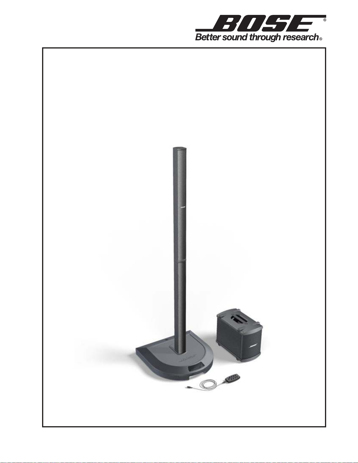
L1® Model I System
L1 Model I Power Stand, L1 Model I Cylindrical Radiator®,
R1 Remote Control and B1 Bass Module
US/Canada, Japan, European, UK and Australian Versions
©2010 Bose Corporation
Service Manual
Reference Number 302233-SM Rev . 04
Electronic Copy Only
Page 2

Contents
Safety Information .....................................................................................................................................................3
Specifications ........................................................................................................................................................ 4-5
Differences between the PS1 Power Stand and the L1
Electrostatic Discharge Sensitive (ESDS) Device Handling ..................................................................................6
Warranty.....................................................................................................................................................................6
Part List Notes ...........................................................................................................................................................6
Packaging Part List, L1 Model I Power Stand (see Figure 1).................................................................................7
Figure 1. L1 Model I Power Stand Packaging V iew.....................................................................................................8
Packaging Part List, L1 Model I Line Array (see Figure 2) .....................................................................................9
Figure 2. L1 Model I Line Array Packaging View.........................................................................................................9
Packaging Part List, B1 Bass Module (see Figure 3) ...........................................................................................10
Figure 3. B1 Bass Module Packaging View...............................................................................................................10
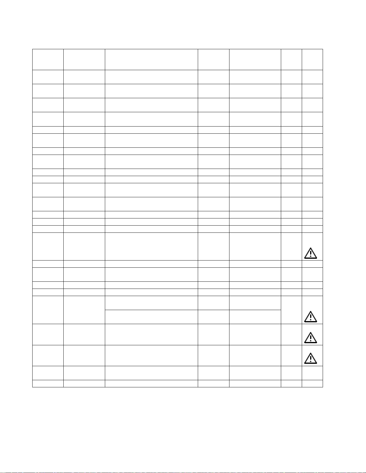
Main Part List, L1 Model I Power Stand (see Figure 4) ........................................................................................11
Figure 4. L1 Model I Power Stand Exploded V iew.....................................................................................................12
Main Part List, L1 Model I Power Box (see Figure 5) ...........................................................................................13
Figure 5. L1 Model I Power Box Exploded View .......................................................................................................13
Main Part List, L1 Model I Input Panel Assembly (see Figure 6) .........................................................................14
Figure 6. L1 Model I Input Panel Assembly Exploded View ......................................................................................15
Main Part List, Remote Control Assembly (see Figure 7) ....................................................................................16
Figure 7. Remote Control Assembly Exploded V iew .................................................................................................16
Main Part List, L1 Model I Upper and Lower Line Source Arrays (see Figure 8) ...............................................17
Figure 8. L1 Model I Line Array Exploded View.........................................................................................................18
Main Part List, B1 Bass Module Exploded View (see Figure 9)...........................................................................19
Figure 9. B1 Bass Module Exploded View ................................................................................................................19
Electrical Part Lists ........................................................................................................................................... 20-69
Input Panel PCB Assembly............................................................................................................................... 20-29
Digital Signal Processor (DSP) PCB Assembly .............................................................................................. 30-36
Microprocessor (MCU) PCB Assembly............................................................................................................ 37-40
Amplifier PCB Assembly , Part Number 306282............................................................................................... 41-47
Amplifier PCB Assembly , Part Number 312945............................................................................................... 48-52
27 V olt Switch-Mode Power Supply PCB Assembly....................................................................................... 53-57
Auxiliary Power Supply PCB Assembly .......................................................................................................... 58-63
FCC Filter PCB Assembly................................................................................................................................. 64-66
Remote Control PCB Assembly ....................................................................................................................... 67-69
Figure 10. L1 Model I Power Stand Electronics Module with Top Cover Removed ...................................................70
Disassembly Procedures.................................................................................................................................. 71-77
Figure 1 1. L1 Model I Power Stand Block Diagram ...................................................................................................78
T est Procedures ................................................................................................................................................ 79-85
Figure 12.
L1 Model I Power Stand Sof tware Update Procedure ..........................................................................................90
Theory of Operation ......................................................................................................................................... 91-111
Schematic Diagrams ....................................................................................................................................112-133
Line Array Wiring Diagram ................................................................................................................................134
Figure 13. EMI (FCC) Filter PCB Assembly Board Layout...................................................................................135
Figure 14. +/-27V SMPS PCB Assembly Board Layout .......................................................................................135
Figure 15. Auxiliary P/S PCB Assembly Board Layout ........................................................................................135
Figure 16. Input Panel PCB Assembly Top Etch Board Layout ............................................................................136
Figure 17. Input Panel PCB Assembly Bottom Etch Board Layout .....................................................................136
Figure 18. DSP PCB Assembly Top Etch Board Layout ......................................................................................137
Figure 19. DSP PCB Assembly Bottom Etch Board Layout ................................................................................137
Figure 20. MCU PCB Assembly Top Etch Board Layout......................................................................................138
Figure 22. Remote Control PCB Assembly Top Etch Board Layout .....................................................................138
Figure 21. MCU PCB Assembly Bottom Etch Board Layout ................................................................................138
Figure 23. Remote Control PCB Assembly Bottom Etch Board Layout .............................................................. 138
Figure 24. Class-D Amplifier PCB Assembly, P/N: 306282, Top Etch Layout ..................................................... 139
Figure 25. Class-D Amplifier PCB Assembly, P/N: 306282, Bottom Etch Layout ............................................... 139
Figure 26. Class-D Amplifier PCB Assembly, P/N: 312945, Top Etch Layout ..................................................... 140
Figure 27. Class-D Amplifier PCB Assembly, P/N: 312945, Bottom Etch Layout ............................................... 140
IC Diagrams ...................................................................................................................................................141-153
Service Manual Revision History ......................................................................................................................154
Amplifier Output Test Cable Wiring Diagram ............................................................................................86
®
Model I Power Stand ............................................6
2
Page 3

Safety Information
1. Parts that have special safety characteristics are identified by the symbol on schematics
or by special notes on the parts list. Use only replacement parts that have critical characteristics
recommended by the manufacturer.
2. Make leakage current or resistance measurements to determine that exposed parts are
acceptably insulated from the supply circuit before returning the unit to the customer.
Use the following checks to perform these measurements:
A. Leakage Current Hot Check-With the unit completely reassembled, plug the AC line cord
directly into a 120V AC outlet. (Do not use an isolation transformer during this test.) Use a
leakage current tester or a metering system that complies with American National Standards
Institute (ANSI) C101.1 "Leakage Current for Appliances" and Underwriters Laboratories (UL)
6500 / IEC 60056 paragraph 9.1.1. With the unit AC switch first in the ON position and then in
OFF position, measure from a known earth ground (metal waterpipe, conduit, etc.) to all exposed metal parts of the unit (antennas, handle bracket, metal cabinet, screwheads, metallic
overlays, control shafts, etc.), especially any exposed metal parts that offer an electrical return
path to the chassis. Any current measured must not exceed 0.5 milliamp. Reverse the unit
power cord plug in the outlet and repeat test. ANY MEASUREMENTS NOT WITHIN THE
LIMITS SPECIFIED HEREIN INDICATE A POTENTIAL SHOCK HAZARD THAT MUST BE
ELIMINATED BEFORE RETURNING THE UNIT TO THE CUSTOMER.
B. Insulation Resistance Test Cold Check-(1) Unplug the power supply and connect a jumper
wire between the two prongs of the plug. (2) Turn on the power switch of the unit. (3) Measure
the resistance with an ohmmeter between the jumpered AC plug and each exposed metallic
cabinet part on the unit. When testing 3 wire products, the resistance measured to the product
enclosure should be between 2 and infinite MOhms. Also, the resistance measured to exposed
input/output connectors should be between 4 and infinite MOhms. When testing 2 wire products, the resistance measured to exposed input/output connectors should be between 4 and
infinite MOhms. If it is not within the limits specified, there is the possibility of a shock hazard,
and the unit must be repaired and rechecked before it is returned to the customer.
CAUTION: The Bose® L1® Model I System contains no user-serviceable parts. To pre-
vent warranty infractions, refer servicing to warranty service stations or factory service.
PROPRIETARY INFORMATION
THIS DOCUMENT CONTAINS PROPRIETARY INFORMATION OF
BOSE CORPORATION WHICH IS BEING FURNISHED ONLY FOR
THE PURPOSE OF SERVICING THE IDENTIFIED BOSE PRODUCT
BY AN AUTHORIZED BOSE SERVICE CENTER OR OWNER OF
THE BOSE PRODUCT, AND SHALL NOT BE REPRODUCED OR
USED FOR ANY OTHER PURPOSE.
3
Page 4

Specifications
MECHANICAL
External Dimensions
®
Model I Cylindrical Radiator®: Height: 86.0 in (2184 mm)
L1
Width: 3.5 in (89 mm)
Depth: 4.0 in (105 mm)
L1 Model I Power Stand: Height: 5.0 in (127 mm)
Width: 26.0 in (660 mm)
Depth: 26.0 in (660 mm)
B1 Bass Module: Height: 15.3 in (380 mm)
Width: 10.3 in (257 mm)
Depth: 18.0 in (457 mm)
R1 Remote: Height:1.6 in (40 mm)
Width: 2.8 in (71 mm)
Depth: 5.6 in (141 mm)
Weight
L1 Model I Cylindrical Radiator: 14.5 lbs (6 kg) Upper
16.0 lbs (7 kg) Lower
L1 Model I Power Stand: 35 lbs (16 kg)
B1 Bass Module: 25 lbs (12 kg)
R1 Remote: 0.6 lbs (0.27 kg)
Transducer Complement
L1 Model I Cylindrical Radiator: 24 x 2.25 in (57 mm) Drivers - 4 ohms
B1 Bass Module: 2 x 5.25 in (133 mm) Drivers - 8 ohms
ACOUSTICAL
Frequency Response
L1 Model I Cylindrical Radiator: 120 Hz to 15 kHz
B1 Bass Module: 40 Hz to 250 Hz
L1 Model I System (with system EQ): 40 Hz to 15 kHz
Port Tuning
L1 Model I Cylindrical Radiator: 114 Hz
B1 Bass Module: 44 Hz
4
Page 5

Specifications
ELECTRICAL
Impedance
®
L1
Model I Cylindrical Radiator®: 4 ohms nominal, both sections in parallel
Lower Model I line array section: 8 ohms nominal
Upper Model I line array section: 8 ohms nominal
B1 Bass module (optional): 8 ohms nominal
System Power Handling
(Continuous full power per IEC-268-5 for duration of 100 hours)
L1 Model I Cylindrical Radiator: 250 W
B1 Bass module: 125 W
L1 Model I Power Stand
Rated Power: 2 x 250 W/Ch/4 ohm. (all channels operating)
Output Level: Line Out: Bal XLR, +4dBu
Bass-Line Out: Bal TRS, -4dBu (nom) +9dBu max
Unbal TS, -10dBu (nom) +3dBu max
Efficiency: 80% minimum
THD at Rated Power: 1.0% Max @ 30 Hz - 15 KHz @ 4 ohms/Ch.
THD at -3dB (~125W): 0.25% Max @ 30 Hz - 15 KHz @ 4 ohms/Ch.
S/N ratio: -80dB minimum, referenced to full power
Frequency Response: 40 Hz-15 KHz +/-3 dB @ R load = 4-16 ohms
Thermal: Operate 2Ch. x 83 W Continuous @ 4 ohms,
50°C ambient with No Shut-Down
AC Power Rating: US/Canada: 100-127V, 50/60Hz 1000W
International: 220-240V, 50/60Hz 1000W
Max Power Draw: 1400 watts 50/60 Hz
Peak In Rush Current: US/Canada: 32 A @ 120V, 60 Hz
International: 16A @ 230V, 60Hz
Power Supply Voltages: Channels 1 and 2 SMPS 27.5 VDC +/-2%
Auxiliary supply #1 +5 VDC/1 A +/- 3%
Auxiliary supply #2 +3.3 VDC/1.5 A +/- 3%
Fan 1.2.3.4 Voltage: +24 VDC +/-1V
5
Page 6

Differences between the PS1 Power Stand and the L1® Model I Power Stand
The L1 Model I Power St and is very similar to the Personalized Amplification System PS1 Power
Stand. There are some significant differences, however:
1. The line array is now powered by one 250W amplifier instead of two. The two line array
sections (upper and lower) are now wired in parallel and powered by a single amplifier. Each
line array section impedance is now 8 ohms, with the two sections wired in parallel, for a total of
4 ohms in operation. The line arrays sections used with the PS1 power stand were 4 ohms
each. Due to optimization of the speaker to the amplifier, the overall output level of the L1 Model
I system is virtually the same as the PAS system. There is a mechanical stop to prevent users
from plugging a PAS line array into an L1 Model I power stand. Users can however insert an L1
Model I line array into a PAS PS1 Power Stand. This will not harm the unit, but will result in a
lower output level (~1.5 dB less).
2. The Amp 1 IN, Amp 2 IN, Amp 3 IN, All Amps IN, Amp 1 OUT and Amp 2 OUT jacks have
been removed from the L1 Model I Power Stand. These connectors were originally intended for
users to access the power stand amplifiers in a stand-alone fashion. They were rarely used on
the PS1 Power Stand.
CAUTION: Be sure to use only L1 Model I upper and lower line array sections with the L1 Model
I power stand. It is physically possible to connect a PAS upper line array section onto an L1
Model I lower line array section. Doing so will result in an excessive current drain on the L1
Model I power stand amplifier board, possibly causing a failure.
Electrostatic Discharge Sensitive (ESDS)
Device Handling
This unit contains ESDS devices. We recommend the following precautions when repairing,
replacing or transporting ESDS devices:
• Perform work at an electrically grounded work station.
• Wear wrist straps that connect to the station or heel straps that connect to conductive
floor mats.
• Avoid touching the leads or contacts of ESDS devices or PC boards even if properly
grounded. Handle boards by the edges only.
• Transport or store ESDS devices in ESD protective bags, bins, or totes. Do not insert
unprotected devices into materials such as plastic, polystyrene foam, clear plastic bags,
bubble wrap or plastic trays.
W arranty
The Bose
The L1 Model I line array and the B1 bass module are covered by a 5-year limited warranty.
®
L1 Model I System electronics are covered by a limited 1-year transferable warranty.
Part List Notes
1. This part is not normally available from Customer Service. Approval from the Field Service
Manager is required before ordering.
2. The individual parts located on the PCBs are listed in the Electrical Part List.
3. This part is critical for safety purposes. Failure to use a substitute replacement with the
same safety characteristics as the recommended replacement part might create shock, fire
and/or other hazards.
4. This part is referenced for informational purposes only. It is not stocked as a repair part. Refer
to the next higher assembly for a replacement part.
6
Page 7
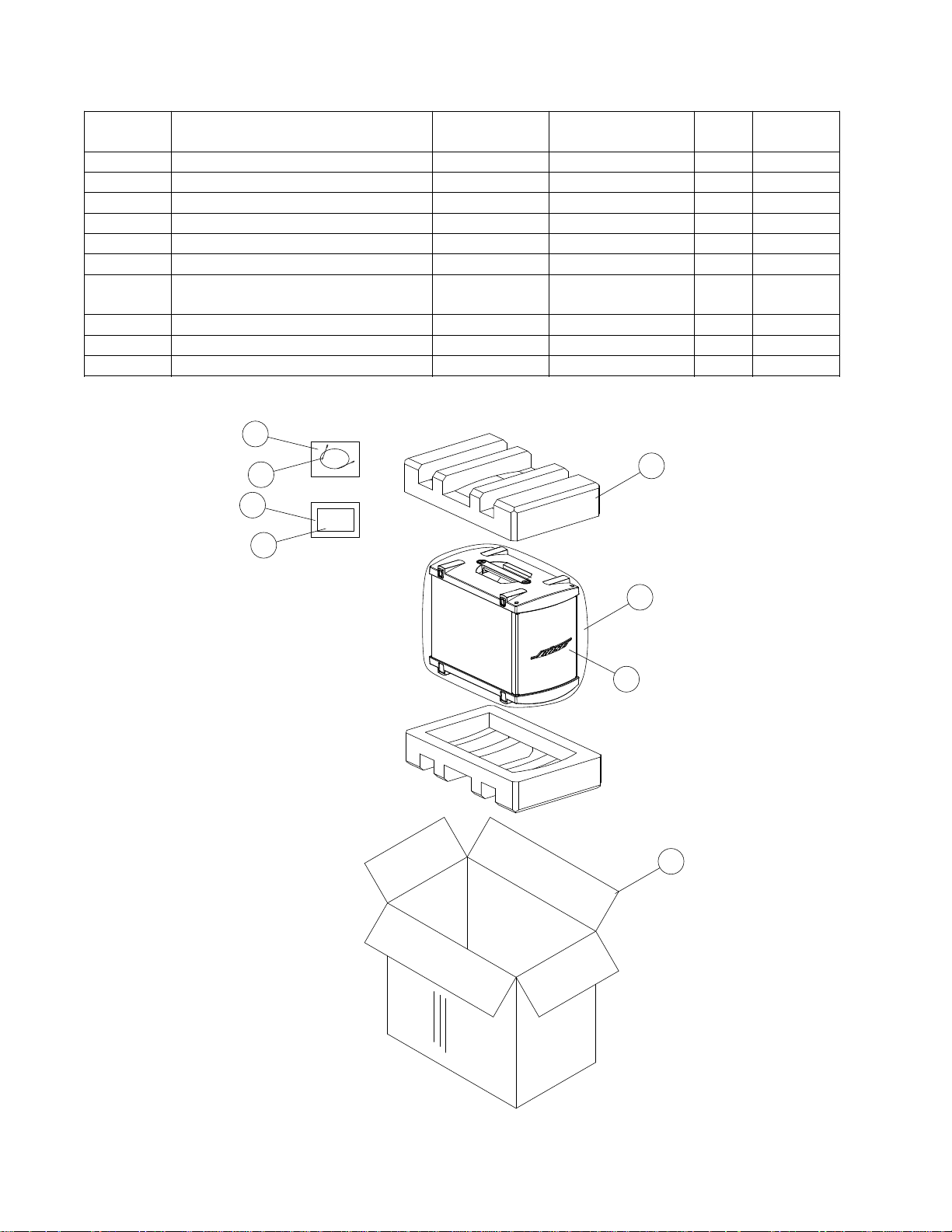
Packaging Part List
L1® Model I Power St and (see Figure 1)
Item
Number
- Carton Kit, Includes Carton,
Cardboard A & B, and Packing
PE Foams 1 – 4.
1 PS1 Filler Card Board - A 275437 1450-7370+1 2
2 Carry Bag for Power Stand 275468 8901-4920-0 1
3 Poly Bag for Carry Bag - 1497-7572-0 1 4
4 Poly Bag - 1497-1062-0 1 4
5 Owner’s Manual, DVD
Owner’s Manual, CD, Japan
6 Quickstart Guide 278815-02 - 1
7 Poly Bag, 10”x12” - 1497-4102-0 3 4
8 7-Pin MIDI Cable 035403 7012-6620-2 1
9 PS1 Filler PE - Foam 4 275442 1493-0421+3 2
10 PS1 Filler PE - Foam 2 275440 1493-0411+3 1
11 L1 Model I Power Stand Assy - REF 1 4
12 Poly Bag for Power Stand - 1497-7572-0 1 4
13 PS1 Filler PE - Foam 3 275441 1493-0401+3 2
14 R1 Remote Control Assembly
w/packaging
15 PS1 Filler PE - Foam 1 275439 1493-0391+3 1
16 PS1 Filler Card Board - B 275438 1450-7410+4 4
17 Carton, PS1 Power Stand 275846 1436-4302+3-3 1
18 Line Cord, 120V, 15A, US/Can 035393 - 1 3
Line Cord, 230V, 15A, Euro 283048 SVC-PS121+AAC 1
Line Cord, 230V, 15A, Aus 283623 7012-5430+0 1
Line Cord, 230V, 15A, UK 283624 7010-9810+0 1
Line Cord, 100V, 15A, Japan 298167 SVC-PS101+AAC 1
19 Poly Bag for Fuse - 1497-0332-0 1 4
20 Fuse, T15A, 125V/250V,
6.3x32mm, US/Can/Japan
Fuse, T10A, 125V/250V,
6.3x32mm, Euro/UK/Aus
Description Bose® Part
Number
307131 SVC-PS111+CKIT 1
306618
306316-01
035394 SVC-PS111+REM 1
307732 5120-0023+0 1 3
279425 5120-0170+0 1
Vendor Part
Number
8901-5080+1
4115-0009+0
Qty. Note
1
7
Page 8
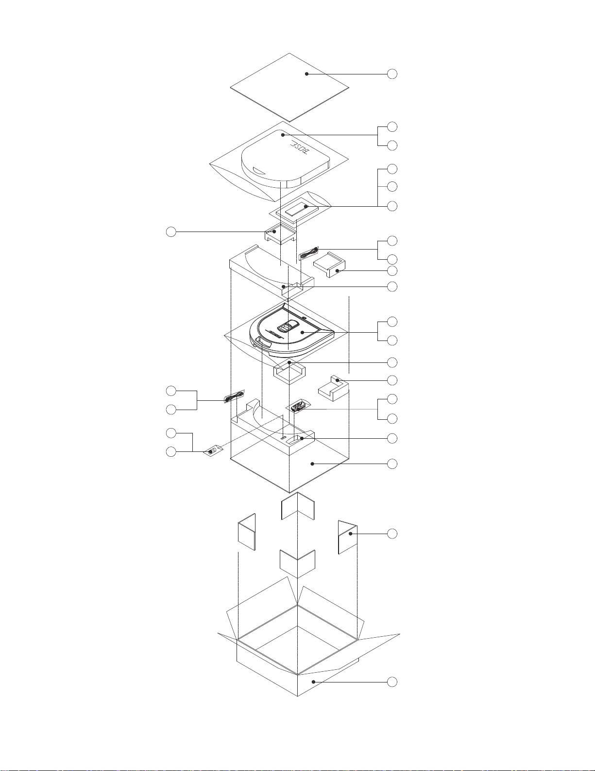
1
2
3
4
5
6
9
7
18
19
20
7
8
9
10
11
12
13
13
7
14
15
1
Figure 1. L1
16
17
®
Model I Power Stand Packaging View
8
4x
Page 9
Packaging Part List
L1® Model I Line Array (see Figure 2)
Item
Number
- Carton Kit, Includes Cardboard
Description Bose® Part
Number
307132 - 1
Vendor Part
Number
Qty. Note
A and B, and Packing PE
Foams 1 - 5
1 Packing PE Foam 4 307719 1493- 0461-0 1
2 Packing PE Foam 2 307717 1493- 0441-0 2
3 Poly Bag - 1497-7562-0 2 4
4 Packing PE Foam 1 307716 1493- 0431-0 1
5 Packing Cardboard A 307720 1450-7380-0 2
6 Packing PE Foam 5 306626 1493- 0471-0 1
7 Line Sour ce Lower Assembly REF - 1
8 Line Source Upper Assembly REF - 1
9 Line Source Carry Bag 275470 - 2
10 Poly Bag for Carry Bag - - 2 4
11 Packing Cardboard B 306628 1450-7400-0 1
12 Packing PE Foam 3 307718 1493-0451-0 1
13 Carton, no fillers 306629 1437-9702+1-3 1
1
5
2
3
3
4
2
6
7
8
9
10
11
12
5
Figure 2. L1 Model I Line Array Packaging View
9
13
Page 10
Packaging Part List
B1 Bass Module (see Figure 3)
Item
Number
Description Bose® Part
Number
Vendor Part
Number
Qty. Note
- Carton Kit – Includes All Fillers 307133 - 1
1 Carton Filler, PE Foam 303838 - 2
2 Poly Bag, 12x16x49” - 1497-4552-0 1
3 B1 Bass Module REF - 1
4 Bass Module Carton, No Fillers 303837 - 1
5 Bubble Bag for Cable - 1497-1122-0 1
6 4-Wire Speakon Cable
035404 7012-6620-2 1
Assembly
7 Poly Bag for Instruction Manual - 1497-1062-0 1
8 Owner's Manual 303154 - 1
- Carry Bag for Bass Module 035025 - 1
5
2x
6
7
8
1
2
3
4
Figure 3. B1 Bass Module Packaging View
10
Page 11
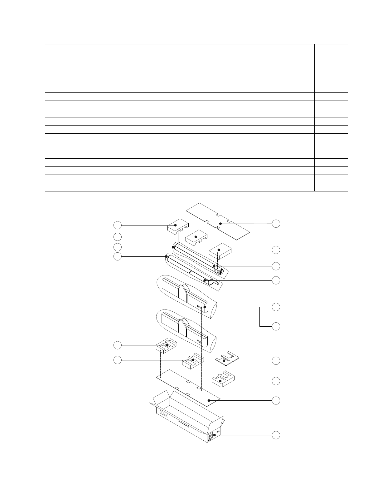
Main Part List
L1® Model I Power St and (see Figure 4)
Item
Number
1 Screw, Mach, M4x14, Blk, Zinc 276999 2904-4014-3000 19
2 Screw, Mach, M4x8, Blk, Zinc 276997 2904-4008-3000 4
3 Housing, Lower, Power Stand 264035 SVC-PS111+LCAB 1
4 Power Sta nd Ca vit y Assem bly,
consists of:
Plate, Base, Power Stand - 1404-9601-0 1 4
PS1 Slide Spring - 2510-3611-0 1 4
Screw, Flat-CS, M2.6x8, BZ - 2901-2608-3001 4 4
Screw, Mach, M6x35mm, Blk, Zinc,
Slide Block
Screw, Mach, M4x8 276997 2904-4008-3000 2 4
Cavity, Aluminum, Power Stand - 4135-3731-0 1 4
Guide, Cavity, Power Stand - 4135-3741-0 1 4
Latch, Power Stand - 4135-3751-0 1 4
Slide, Power Stand - 4135-3761-0 1 4
Plate, Latch, Power Stan d - 4135-3771-0 1 4
Post, Copper, Power Stand - 4135-3971-0 1 4
Pedal, Foot, Power stand - 4154-6921-0 1 4
Screw, Mach, M4x14, Blk, Zinc 276999 2904-4014-3000 4
Screw, Mach, M3x8, Blk, Latch Plate - 2901-3008-3000 4 4
Gasket, EVA, 5x500mm - 4153-3331-0 2 4
5 Power Box As sembly, includes PCBs
US/Canada, 120V
Euro, UK, Aus, 230V
Japan, 100V
6 Screw, Mach, M3x10, Blk, Zinc - 2900-3010-3030 16 4
7 Housing, Upper, Power Stand 264034 1466-4801-0 1
8 Power Sta nd Prot ec ti ve Plu g 035410 4154-7251-0 1
9 Power Sta nd Foot Pe dal 264039 4154-692 1-0 1
10 DSP PCB Assembly 283364 SVC-PS111+DSP 1 2
11 MCU PCB Assembly 306284 SVC-PS111+MCU 1 2
12 Input PCB Assembly 306283 SVC-PS111+INP1 1 2
13 Input Panel Assembly, includes DSP,
MCU and Input PCBs
US/Can, 120V
Euro, UK, Aus, 230V
Japan, 100V
14 Power Stand Push Button 2639 79 2446-4901-0 4
15 Screw, Mach, M3x10, Input Panel 277004 2911-3010-3000 18
16 Power Stand V/R Knob 263986 2446-630 1-0 4
17 Power Stand Door Assy, includes: 273727 SVC-PS111+DOOR 1
Cover, I/O, Power Stand - 1466-5001-0 1 4
Knob, I/O Cover - 2446-6001-0 1 4
Latch, I/O Cover - 4154-6931-0 1 4
Latch Spring, I/O Cover - 2510-3531-0 1 4
Screw, M3x10, TTB, FH, BZ-PCB 277004 2911-3010-3000 1
- Power Stand Cavity Harness Assy 307730 SVC-PS111+MOLEX 1
- EQ Preset Label
US/Can
Euro, UK, Aus
Japan
Description Bose®
Part
Number
306279 SVC-PS111+FOOT 1
- 2903-6035-3000 1 4
306280
306286
312943
306281
306287
312944
306317
283831
311832
Vendor
Part Number
SVC-PS111+PBOX
SVC-PS121+PBOX
SVC-PS101+PBOX
SVC-PS111+PANEL
SVC-PS121+PANEL
SVC-PS101+PANEL
3001-1756+0
3001-1756+0
3001-2111+0
Qty Note
1 1
1 1
1
11
Page 12
15x
1
4x
2
3
4x
1
4
14x
3x
1110
18x
6
6
12
15
17
5
7
8
9
13
14
16
4x
4x
Figure 4. L1
®
Model I Power Stand Exploded View
12
Page 13
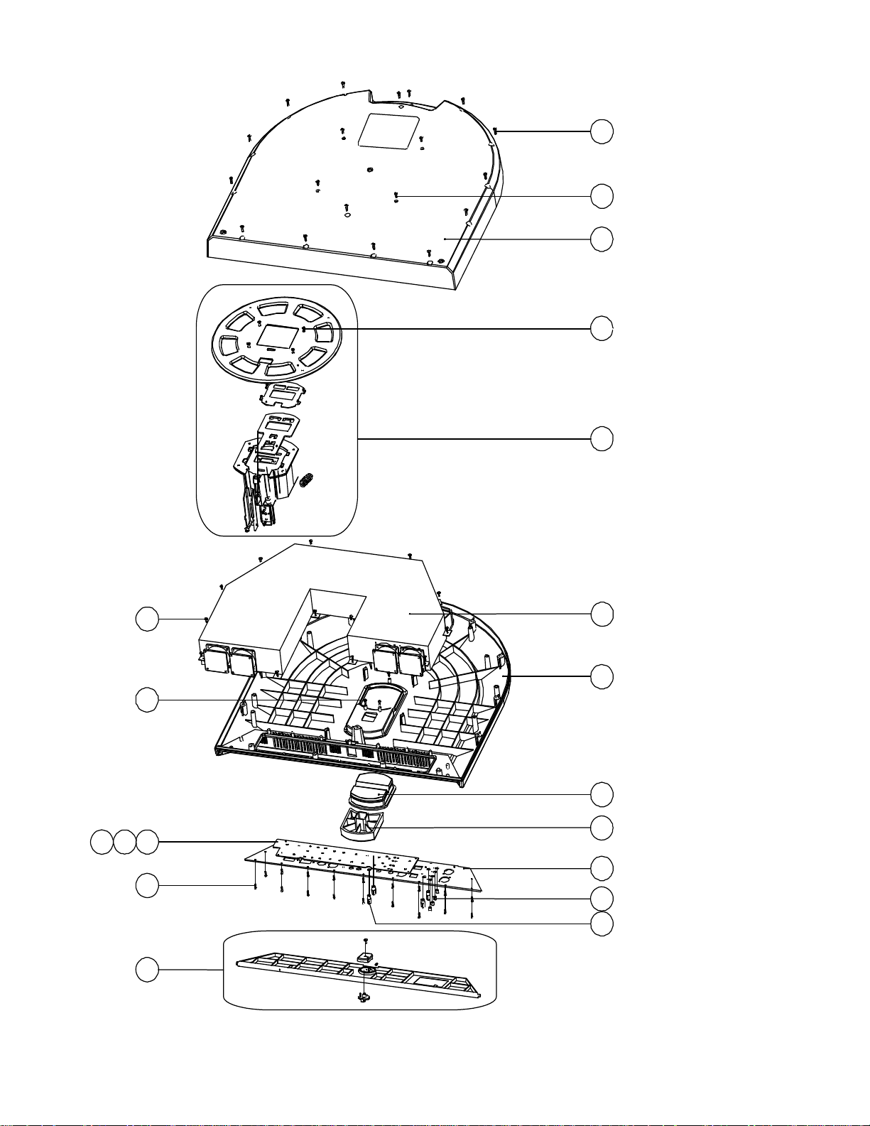
Main Part List
V
L1® Model I Power Box (see Figure 5)
Item
Number
1 Screw, Ma ch , M3x 6m m , Blk , Z inc 277003 2904-3006-3000 24
2 Screw, Ma ch , M3x 10m m , w/ was her 275435 2900-3010-300 0 27
3 D-Class Amp PCB Assem bly ,
US/Can /Eu/UK/Aus (bef or e 3/2/10)
Japan, all DOM ( all 3/2/10 and after )
4 +/- 27V SMPS P CB Ass e mb ly,
US/Canada, Euro, UK, Aus
Japan
5 Aux P ower S upply PCB Assem bly,
US/Canada, Euro, UK, Aus
Japan
6 Fan, 24VDC, 60x60x25mm, 80mA 279143 8913-4007-0 4
7 Screw, Ma ch , M3x 30m m , Blk , Zinc, Fan
Mounting
8 Washer, Spring, M3x0.9x5.0mm - 2607-3009-0553 16 4
9 Washer, Me talid, 3. 3, OD=8, T=0.5 - 2600-3005-0640 16 4
10 FCC Fi lter PCB A ssembly
US/Canada, Japan, 100/ 120V
Euro, UK, A us, 220- 240V
Note: Item 3, D-Class Am p PCB As se m bly , has bee n chan ged to part number 312945 for all
voltage variants starting with DOM 0061
3/2/10 use part num ber 306282.
Description Bose®
Part
Number
306282
312945
307734
312947
307729
312946
277002 2904-3030-3000 16
306285
306288
(3/ 2/10). US/Can/ Eu /UK/A us units built before
endor Part
Number
SVC-PS111+DAMP
SVC-PS101+DAMP
SVC-PS111+AMPP
SVC-PS101+AMPP
SVC-PS111+AUX
SVC-PS101+AUX
SVC-PS111+FCC1
SVC-PS121+FCC2
Qty Note
1 2
2 2
1 2
1 2
16x
24x
1
Top
Cover
27x
10
4
4
5
16x
8
16x
7
4x
6
9
Chassis
2
3
2
3x
Figure 5. L1 Model I Power Box Exploded View
13
Page 14
Main Part List
L1® Model I Input Panel Assembly (see Figure 6)
Item
Number
1 MCU PCB,
2 VR101,
3 VR103,
4 SW102,
5 - PS1 Push Button Knob 263979 2446-4901-0 4
6 J105, J106,
7 J112, J113 Phone Jack, 6.4mm, 9-Pin 275445 2113-1296-0 2
8 J119 Neutrik Speakon Connector,
9 - Bracket, Speakon Jack - 4135-3801-0 3 4
10 - Knob, I/O Panel - 2446-6301-0 4 4
11 J109 RCA Jack, White, 1P,
12 J110 RCA Jack, Black, 1P,
13 J101, J102 Conn., Neutrik, NCJ10FI-V-0 275449 2113-3046-0 2
14 - Push Wheel, Preset Switch 306318 - 2
15 J103, J104 XLR Connector, Neutrik, 3PM 275448 2113-1698-0 2
16 - Fuse Holder, 15A/250VAC, R3-
17 - Screw, M3x10mm 277004 2911-3010-3000 16
18 Screw, M3x12, Csk, Blk,
19 - PS1 DIN Socket, 7-Pin 275454 2113-2013-0 1
20 Screw, AC Inlet Jack, M3x12 - 2900-3012-3000 2 4
21 - Fuse, US/Can/Japan 100/120V,
Fuse, Euro, UK, Aus 220-240V,
22 - AC Inlet Jack 278847 2113-1144-0 1 3
23 - Switch, AC Power, SPST
24 - Washer, Spring,
25 - Nut, M3, Nickel - 2640-3022-0544 2 4
Reference
Designator
DSP PCB
VR102
VR104
SW104
J107, J108
Description Bose®
Part
Number
PCB Support, 12MM High - 4152-0911-0 6 4
Pot, 5k Ohm, 5KX1 10C 275451 4751-0620-0 2
Pot, 20k Ohm, 20KAX1 275450 4751-0580-1 2
Switch, Push, PS828L, 8x8 mm,
MIC
Phone Jack, 6.4mm, 5-Pin 275447 2113-1340-0 7
NL4MD-V
GP 032-09BWG
AU HQ032-09BBG
44A Type, 6.35x32mm,
US/Canada, 120V
Euro, UK, Aus 220-240V
Speakon Connector
T10A, 125V/250V, 6.35x32mm
T10A, 125/250V, 6.35x32mm
US/Canada, Japan, 100/120V
Euro, UK, Aus 220-240V
M3x0.9x5.5mm, BZ
275452 5200-3573-0-00 2
275446 2113-1336-1 3
275444 2113-1950-0 1
275443 2113-1169-1 1
307731
279426
- 2901-3012-3000 6 4
307732 5120-0023+0 1 3
279425 5120-0170-0
278848
279427
- 2607-3009-0553 2 4
Vendor Part
Number
4170-0021+0
4153-1100+0
5200-4826-0
5200-4873-0
Qty. Note
1 3
1 3
14
Page 15
17
13
17
21
22
23
Input Panel
19
18
20
6
7
8
9
16
24
11
25
10
14
15
5
4
2
1
Figure 6. L1
11
3
Input/Output
PCB Assy
DSP PCB
Assy
®
Model I Input Panel Assembly Exploded View
15
1
1
Page 16
Main Part List
Remote Control Assembly (see Figure 7)
Item
Number
1 Knob, VR, Remote Control 263995 2446-5501+1 9
2 Housing, Upper 263997 1466-3701+0 1
3 LED, Red/Green, L-115W EGW - 3700-4536+RG 2 4
4 Variable Resistor, 50KBx1, LM=20MM,
RVO9AC-40-20F-B50K-OC
5 Variable Resistor, 50KBx1, LM=20MM,
RVO9AC-40-20F-B50K
6 Screw, Tapping, 2x6MM - 2954-2006+0000 4 4
7 Washer, Metal, M3x0.9x4MM - 2600-3003+0402 4 4
8 PCB Assembly, Remote Control - 1725-676A+0002 1 4
9 Fiber Sheet - 3100-6341+0 1 4
10 DIN Socket, 7-Pin - 2113-2013+0 2 4
11 Housing, Lower 263996 1466-3601+0 1
12 Screw, 2.6x8MM, CS, Flat Black - 2921-2608+3000 4 4
13 Product Label - 3001-1742+0 1 4
14 Dual Lock Re-closable Fastener - 3100-6311+0 1 4
Description Bose®
Part
Number
- 4751-0600+0 6 4
- 4751-0610+0 3 4
Vendor Part
Number
Qty Note
Figure 7. Remote Control Assembly Exploded View
16
Page 17
Main Part List
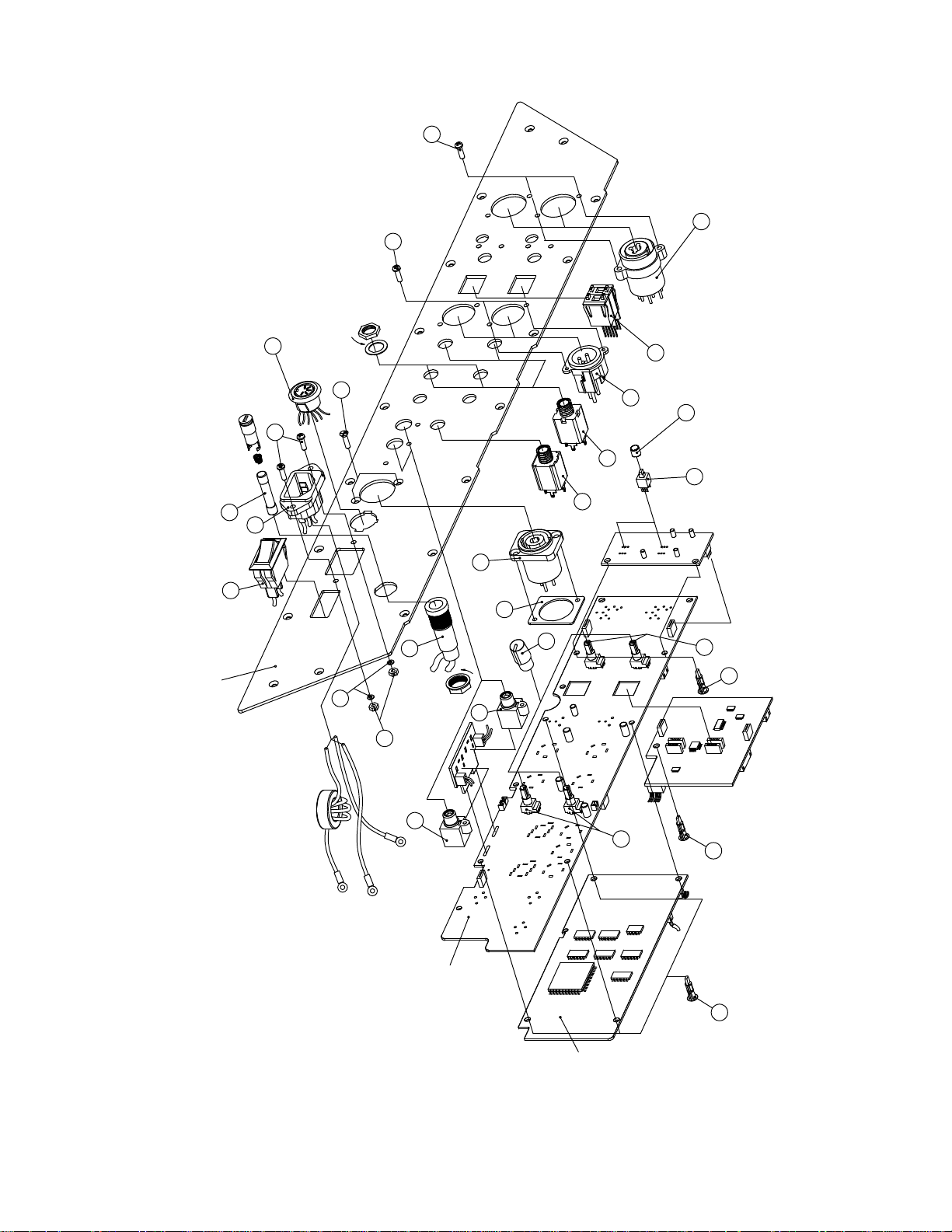
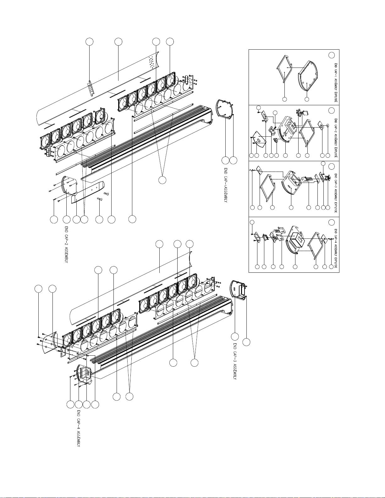
L1® Model I Upper and Lower Line Source Arrays (see Figure 8)
Item
Number
1 End-Cap #1 Assembly, consists of: 273753 1
End-Cap, Top, Upper, Line Source 4154-6661-0 1 4
End-Cap Gasket 4149-0491-0 1 4
2 End-Cap #2 Assembly, consists of: 273787 1
End-Cap, Bottom, Upper, Line Source 4154-6671-0 1 4
Gasket, Cap, Line Source 4149-0491-0 1 4
Airproof Sheet, End Cap, Line Source 4154-6841-0 1 4
Conn Assy, Molex, 4P, AWG#20, UL10 07 7012-6615-0 1 4
Plate, Connector, 4 Pin, Floating, LS 4135-3511-0 1 4
Latch, Locking Mechanism, LS 4135-3541-0 1 4
Cover, Locking Mechanism, LS 4135-3551-0 1 4
Slide Locking Spring 1 4
Slide, Latch, Locking Mechanism, LS 4154-6631-0 1 4
3 End-Cap #3 Assembly, consists of: 273788 1
End-Cap, Top, Lower, Line Source 4154-6641-0 1 4
Gasket, Cap, Line Source 4149-0491-0 1 4
Airproof Sheet, End Cap, Line Source 4154-6841-0 1 4
Header, Vertical, Molex, 4P 2101-1438-0 1 4
Plate, Connector, 4 Pin, Fixed, LS 4135-3501-0 1 4
PCB, Molex, 10p & 4P 1725-684A-0000 1 4
Conn Assy, AWG#20, UL1015, L= 150m m 7012-6616-0 1 4
4 End-Cap #4 Assembly, consists of: 312010 1
End-Cap, Bottom, Lower, Line Source 4154-6651-0 1 4
Gasket, Cap, Line Source 4149-0491-0 1 4
Airproof Sheet, End Cap, Line Source 4154-6841-0 1 4
Header, Vertical, Molex, 10P 2101-1437-0 1 4
PCB, Molex, 10p & 4P 1725-684A-0000 1 4
Plate, Connector, 10PIN, Fixed, LS 4135-3531-0 1 4
Conn Assy, AWG#20, UL1015, L= 150m m 7012-6616-0 1 4
5 Screw, M3x10, Tapping - 2950-3010-3000 24 4
6 Line Source Driver Assembly 303836 SVC-WF+BSPAL2 24
7 Line Source Driver Screws - - 96 4
8 Front Baffle, Upper, Assembly,
consists of:
Front Baffle-1 1404-9001-0 3 4
Baffle Gasket-1 4149-0431-0 6 4
9 Front Baffle, Lower, Assembly,
consists of:
Front Baffle-2 1404-9101-0 1 4
Baffle Gasket-1 4149-0431-0 6 4
10 Screws, Front Baffle - - 16 4
11 Grille, Lower, Assembly (w/gaskets) 263996 - 1
12 Nameplate, Bose Logo, Line Source 264024 -
13 Line Source Bayonet Assembly 035407 8901-4270-0 1
14 Line Source Bayonet Screws - - 2 4
15 Grille, Upper, Assembly (w/gaskets) 264017 4135-3571-0 1
16 Cove r Plate, Lower Array - - 1 4
17 Screws, Lower Array Cover Plate - - 4 4
18 Washer, Lower Array Cover Plate - - 4 4
19 Nut, Lower Array Cover Pla te - - 4 4
Description Bose®
Part
Number
273836 - 1
273837 1
Vendor Part
Number
Qty Note
17
Page 18
12
11
6
7
L1 Upper Array
Assembly
1234
B
K
H
M
5
1
L
G
J
F
I
A
C
E
D
B
K
8
Q
S
D
13
2
5
14
8
10
7
10
L1 Lower Array
Assembly
15
6
7
6
K
W
V
R
B
Q
U
T
O
N
P
S
D
B
17
16
3
5
10
10
19
18
4
5
9
Figure 8. L1
®
Model I Line Array Exploded View
8
18
Page 19
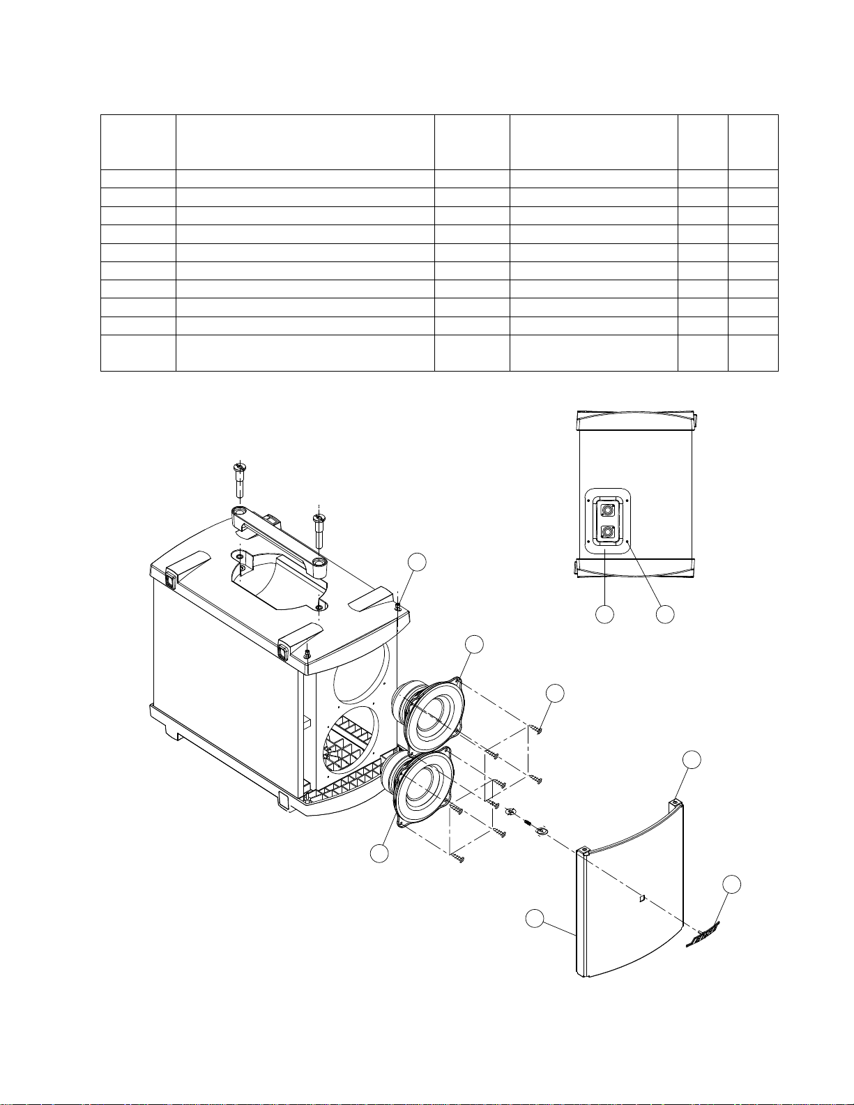
Main Part List
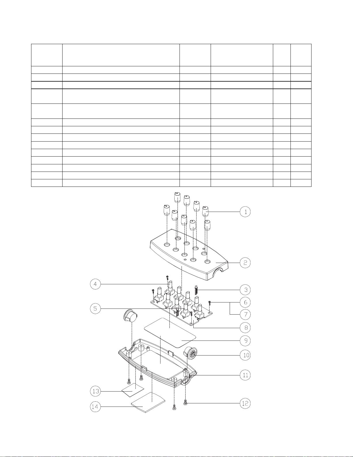
B1 Bass Module Exploded View (see Figure 9)
®
Item
Number
1 Screw, M4 X 28, BK, B1 Grille - 2908-4028-3400 4 4
2 Woofer Assembly 263998 SVC-FM040C-WF 2
3 Gasket, Woofer Assembly - - 2 4
4 Screw, M4 X 16, BK, B1 Driver - 2913-4016-3000 8 4
5 Grille Assembly 263992 SVC-FM040C-GRILL 1
6 Gasket, Grille Assembly - - 2 4
7 Logo Assembly - - 1 4
8 B1 Terminal Panel Assembly 276409 SVC-FM040C-TML 1
9 Screw, M3 X 12, BK, B1 Input Cup - 2900-3012-3000 4 4
- 4-Wire Speakon to Speakon Cable
Assembly, L=1.5M
Description
Bose
Part
Number
035404 SVC-FM040C-CABLE 1
Vendor Part Number Qty Note
124x
8
2x
48x
32x
62x
9
5
7
Figure 9. B1 Bass Module Exploded View
19
Page 20

Electrical Part List
Input Panel PCB Assembly
Resistors
Reference
Designator
R101 10M, RMG, 0805, 1/10W, 1% 4720-106A+J 4
R102 1M, RMG, 0805, 1/10W, 1% 4720-105A+J 4
R103 51 O HM, RMG, 0805, 1/10W, 1% 4720-510A+J 4
R104 1K, RMG, 0805, 1/10W, 1% 4720-102A+J 4
R105 15K, RMG, 0805, 1/10W, 1% 4720-153A+J 4
R106 51 O HM, RMG, 0805, 1/10W, 1% 4720-510A+J 4
R107 15K, RMG, 0805, 1/10W, 1% 4720-153A+J 4
R108 15K, RMG, 0805, 1/10W, 1% 4720-153A+J 4
R109 10K, RMG, 0805, 1/10W, 1% 4720-103J+J 4
R110 22K, RMG, 0805, 1/10W, 5% 4720-223J+J 4
R111 5. 6K, RMG, 0805, 1/10W, 5% 4720-562J+J 4
R112 1M, RMG, 0805, 1/10W, 1% 4720-105J+J 4
R113 10K, RMG, 0805, 1/10W, 1% 4720-103J+J 4
R114 22K, RMG, 0805, 1/10W, 5% 4720-223J+J 4
R115 5. 6K, RMG, 0805, 1/10W, 5% 4720-562J+J 4
R116 1M, RMG, 0805, 1/10W, 1% 4720-105J+J 4
R117 100 O HM, RMG, 0805, 1/10W, 1% 4720-101J+J 4
R118 33K, RMG, 0805, 1/10W, 1% 4720-333A+J 4
R119 10K, RMG, 0805, 1/10W, 1% 4720-103A+J 4
R120 220 O HM, RMG, 0805, 1/10W, 5% 4720-221J+J 4
R121 10K, RMG, 0805, 1/10W, 1% 4720-103A+J 4
R123 10K, RMG, 0805, 1/10W, 1% 4720-103A+J 4
R124 220 O HM, RMG, 0805, 1/10W, 5% 4720-221J+J 4
R125 1. 2K, RMG, 0805, 1/10W, 5% 4720-122J+J 4
R126 1. 2K, RMG, 0805, 1/10W, 5% 4720-122J+J 4
R127 2K, RMG, 0805, 1/10W, 1% 4720-202A+J 4
R128 2K, RMG, 0805, 1/10W, 1% 4720-202A+J 4
R129 10 O HM, RMG, 0805, 1/10W, 5% 4720-100J+J 4
R130 10 O HM, RMG, 0805, 1/10W, 5% 4720-100J+J 4
R131 10K, RMG, 0805, 1/10W, 1% 4720-103A+J 4
R132 10K, RMG, 0805, 1/10W, 1% 4720-103A+J 4
R133 20 O HM, RMG, 0805, 1/10W, 5% 4720-200J+J 4
R134 1M, RMG, 0805, 1/10W, 1% 4720-105J+J 4
R135 10 O HM, RMG, 0805, 1/10W, 5% 4720-100J+J 4
R136 10M, RMG, 0805, 1/10W, 1% 4720-106A+J 4
R137 1M, RMG, 0805, 1/10W, 1% 4720-105A+J 4
R138 100 O HM, RMG, 0805, 1/10W, 1% 4720-101A+J 4
R139 1K, RMG, 0805, 1/10W, 1% 4720-102A+J 4
R140 10K, RMG, 0805, 1/10W, 1% 4720-103A+J 4
R141 100 O HM, RMG, 0805, 1/10W, 1% 4720-101A+J 4
R142 10K, RMG, 0805, 1/10W, 1% 4720-103A+J 4
R150 15K, RMG, 0805, 1/10W, 1% 4720-153A+J 4
R152 100 O HM, RMG, 0805, 1/10W, 1% 4720-101J+J 4
R153 33K, RMG, 0805, 1/10W, 1% 4720-333A+J 4
R154 10K, RMG, 0805, 1/10W, 1% 4720-103A+J 4
R155 10K, RMG, 0805, 1/10W, 1% 4720-103A+J 4
Description Vendor Part
Number
Note
20
Page 21
Electrical Part List
Input Panel PCB Assembly
Resistors (continued)
Reference
Designator
R157 10K, RMG, 0805, 1/10W, 1% 4720-103A+J 4
R158 220 O HM, RMG, 0805, 1/10W, 5% 4720-221J+J 4
R159 220 O HM, RMG, 0805, 1/10W, 5% 4720-221J+J 4
R162 2K, RMG, 0805, 1/10W, 1% 4720-202A+J 4
R163 2K, RMG, 0805, 1/10W, 1% 4720-202A+J 4
R164 10 O HM, RMG, 0805, 1/10W, 5% 4720-100J+J 4
R165 10 O HM, RMG, 0805, 1/10W, 5% 4720-100J+J 4
R166 10K, RMG, 0805, 1/10W, 1% 4720-103A+J 4
R167 10K, RMG, 0805, 1/10W, 1% 4720-103A+J 4
R168 20 O HM, RMG, 0805, 1/10W, 5% 4720-200J+J 4
R169 1M, RMG, 0805, 1/10W, 1% 4720-105J+J 4
R170 10 O HM, RMG, 0805, 1/10W, 5% 4720-100J+J 4
R171 300 O HM, RMG, 0805, 1/10W, 5% 4720-301J+J 4
R172 100 O HM, RMG, 0805, 1/10W, 1% 4720-101A+J 4
R173 12K, RMG, 0805, 1/10W, 1% 4720-123A+J 4
R174 100 O HM, RMG, 0805, 1/10W, 1% 4720-101J+J 4
R175 300 O HM, RMG, 0805, 1/10W, 5% 4720-301J+J 4
R176 100 O HM, RMG, 0805, 1/10W, 1% 4720-101A+J 4
R177 12K, RMG, 0805, 1/10W, 1% 4720-123A+J 4
R178 100 O HM, RMG, 0805, 1/10W, 1% 4720-101J+J 4
R179 220 O HM, RMG, 0805, 1/10W, 5% 4720-221J+J 4
R180 22K, RMG, 0805, 1/10W, 5% 4720-223J+J 4
R181 51K, RMG, 0805, 1/10W, 5% 4720-513J+J 4
R182 220 O HM, RMG, 0805, 1/10W, 5% 4720-221J+J 4
R183 220 O HM, RMG, 0805, 1/10W, 5% 4720-221J+J 4
R185 51K, RMG, 0805, 1/10W, 5% 4720-513J+J 4
R186 220 O HM, RMG, 0805, 1/10W, 5% 4720-221J+J 4
R187 51K, RMG, 0805, 1/10W, 5% 4720-513J+J 4
R188 150K, RMG, 0805, 1/10W, 5% 4720-154J+J 4
R189 1K, RMG, 0805, 1/10W, 1% 4720-102J+J 4
R190 1K, RMG, 0805, 1/10W, 1% 4720-102J+J 4
R191 30K, RMG, 0805, 1/10W, 5% 4720-303J+J 4
R192 2. 2K, RMG, 0805, 1/10W, 5% 4720-222J+J 4
R193 3. 3K, RMG, 0805, 1/10W, 5% 4720-332J+J 4
R197 51K, RMG, 0805, 1/10W, 5% 4720-513J+J 4
R198 150K, RMG, 0805, 1/10W, 5% 4720-154J+J 4
R199 1K, RMG, 0805, 1/10W, 1% 4720-102J+J 4
R200 1K, RMG, 0805, 1/10W, 1% 4720-102J+J 4
R201 30K, RMG, 0805, 1/10W, 5% 4720-303J+J 4
R202 2. 2K, RMG, 0805, 1/10W, 5% 4720-222J+J 4
R204 3. 3K, RMG, 0805, 1/10W, 5% 4720-332J+J 4
R207 220 O HM, RMG, 0805, 1/10W, 5% 4720-221J+J 4
R208 220 O HM, RMG, 0805, 1/10W, 5% 4720-221J+J 4
R209 100 O HM, RMG, 0805, 1/10W, 1% 4720-101J+J 4
R210 12K, RMG, 0805, 1/10W, 1% 4720-123J+J 4
R211 10 O HM, RMG, 0805, 1/10W, 5% 4720-100J+J 4
Description Vendor Part
Number
Note
21
Page 22

Electrical Part List
Input Panel PCB Assembly
Resistors (continued)
Reference
Designator
R212 100 O HM, RMG, 0805, 1/10W, 1% 4720-101J+J 4
R213 12K, RMG, 0805, 1/10W, 1% 4720-123J+J 4
R214 47K, RMG, 0805, 1/10W, 5% 4720-473J+J 4
R215 100 O HM, RMG, 0805, 1/10W, 1% 4720-101J+J 4
R216 100 O HM, RMG, 0805, 1/10W, 1% 4720-101J+J 4
R217 12K, RMG, 0805, 1/10W, 1% 4720-123J+J 4
R218 47K, RMG, 0805, 1/10W, 5% 4720-473J+J 4
R219 100 O HM, RMG, 0805, 1/10W, 1% 4720-101J+J 4
R220 100 O HM, RMG, 0805, 1/10W, 1% 4720-101J+J 4
R221 12K, RMG, 0805, 1/10W, 1% 4720-123J+J 4
R222 47K, RMG, 0805, 1/10W, 5% 4720-473J+J 4
R223 100 O HM, RMG, 0805, 1/10W, 1% 4720-101J+J 4
R224 2. 7K, RMG, 0805, 1/10W, 5% 4720-272J+J 4
R225 2. 7K, RMG, 0805, 1/10W, 5% 4720-272J+J 4
R226 10K, RMG, 0805, 1/10W, 1% 4720-103A+J 4
R227 10K, RMG, 0805, 1/10W, 1% 4720-103A+J 4
R229 47K, RMG, 0805, 1/10W, 5% 4720-473J+J 4
R230 47K, RMG, 0805, 1/10W, 5% 4720-473J+J 4
R231 10K, RMG, 0805, 1/10W, 1% 4720-103A+J 4
R232 10K, RMG, 0805, 1/10W, 1% 4720-103A+J 4
R234 47K, RMG, 0805, 1/10W, 5% 4720-473J+J 4
R235 47K, RMG, 0805, 1/10W, 5% 4720-473J+J 4
R238 5. 6K, RMG, 0805, 1/10W, 5% 4720-562J+J 4
R239 47K, RMG, 0805, 1/10W, 5% 4720-473J+J 4
R240 47K, RMG, 0805, 1/10W, 5% 4720-473J+J 4
R241 47K, RMG, 0805, 1/10W, 5% 4720-473J+J 4
R242 22K, RMG, 0805, 1/10W, 5% 4720-223J+J 4
R243 5. 6K, RMG, 0805, 1/10W, 5% 4720-562J+J 4
R244 47K, RMG, 0805, 1/10W, 5% 4720-473J+J 4
R245 100K, RMG, 0805, 1/10W, 5% 4720-104J+J 4
R246 100K, RMG, 0805, 1/10W, 5% 4720-104J+J 4
R247 100K, RMG, 0805, 1/10W, 5% 4720-104J+J 4
R248 10K, RMG, 0805, 1/10W, 1% 4720-103A+J 4
R249 10K, RMG, 0805, 1/10W, 1% 4720-103A+J 4
R250 10K, RMG, 0805, 1/10W, 1% 4720-103A+J 4
R251 10K, RMG, 0805, 1/10W, 1% 4720-103A+J 4
R252 22K, RMG, 0805, 1/10W, 5% 4720-223J+J 4
R253 560 O HM, RMG, 0805, 1/10W, 5% 4720-561J+J 4
R254 10K, RMG, 0805, 1/10W, 1% 4720-103A+J 4
R255 10K, RMG, 0805, 1/10W, 1% 4720-103A+J 4
R256 22K, RMG, 0805, 1/10W, 5% 4720-223J+J 4
R257 560 O HM, RMG, 0805, 1/10W, 5% 4720-561J+J 4
R258 100K, RMG, 0805, 1/10W, 5% 4720-104J+J 4
R259 100K, RMG, 0805, 1/10W, 5% 4720-104J+J 4
R260 100K, RMG, 0805, 1/10W, 5% 4720-104J+J 4
R261 100K, RMG, 0805, 1/10W, 5% 4720-104J+J 4
Description Vendor Part
Number
Note
22
Page 23
Electrical Part List
Input Panel PCB Assembly
Resistors (continued)
Reference
Designator
VR101 VAR RES, 5KX1, 10C, LM=25MM, RV09AC-40-
25F-C5K
VR102 VAR RES, 5KX1, 10C, LM=25MM, RV09AC-40-
25F-C5K
VR103 VAR RES, 20KAX1, LM=25MM, ALPHA,
RV09AC-40-25F-A20K
VR104 VAR RES, 20KAX1, LM=25MM, ALPHA,
RV09AC-40-25F-A20K
Reference
Designator
C101 100pF, CC, 0805, 50V, 10%, 1.2X2.0 150F-101K+J-BD 4
C102 0. 1uF, CC, 0805, 50V, 10%, 1.2X2.0 150F-104K+J-BD 4
C106 20pF, CC, 0805, 50V, 5%, 1.2x 2.0 150F-200J+J-BD 4
C107 20pF, CC, 0805, 50V, 5%, 1.2x 2.0 150F-200J+J-BD 4
C110 22uF, CE, 50V, 20%, RLT, 5X11 157F-226M+K-IU 4
C112 22uF, CE, 50V, 20%, RLT, 5X11 157F-226M+K-IU 4
C113 47uF, CE, 35V, 20%, RL, 5x11, SUN 157Q-476M+K-IUI 4
C114 47uF, CE, 35V, 20%, RL, 5x11, SUN 157Q-476M+K-IUI 4
C115 100pF, CC, 0805, 50V, 10%, 1.2X2.0 150F-101K+J-BD 4
C116 100pF, CC, 0805, 50V, 10%, 1.2X2.0 150F-101K+J-BD 4
C117 0. 1uF, CC, 0805, 50V, 10%, 1.2X2.0 150F-104K+J-BD 4
C118 0. 1uF, CC, 0805, 50V, 10%, 1.2X2.0 150F-104K+J-BD 4
C119 100pF, CC, 0805, 50V, 10%, 1.2X2.0 150F-101K+J-BD 4
C123 20pF, CC, 0805, 50V, 5%, 1.2x 2.0 150F-200J+J-BD 4
C124 20pF, CC, 0805, 50V, 5%, 1.2x 2.0 150F-200J+J-BD 4
C127 22uF, CE, 50V, 20%, RLT, 5X11 157F-226M+K-IU 4
C129 22uF, CE, 50V, 20%, RLT, 5X11 157F-226M+K-IU 4
C130 47uF, CE, 35V, 20%, RL, 5x11, SUN 157Q-476M+5-IUL 4
C131 47uF, CE, 35V, 20%, RL, 5x11, SUN 157Q-476M+5-IUL 4
C132 100pF, CC, 0805, 50V, 10%, 1.2X2.0 150F-101K+J-BD 4
C133 100pF, CC, 0805, 50V, 10%, 1.2X2.0 150F-101K+J-BD 4
C134 0. 1uF, CC, 0805, 50V, 10%, 1.2X2.0 150F-104K+J-BD 4
C135 100pF, CC, 0805, 50V, 10%, 1.2X2.0 150F-101K+J-BD 4
C136 10uF, CE, 50V, 20%, RLT, 5X11 157F-106M+K-IU 4
C137 1000pF, CC, 0805, 50V, 10%, 1.2x2.0 150F-102K+J-BD 4
C138 100pF, CC, 0805, 50V, 10%, 1.2X2.0 150F-101K+J-BD 4
C139 10uF, CE, 50V, 20%, RLT, 5X11 157F-106M+K-IU 4
C140 1000pF, CC, 0805, 50V, 10%, 1.2x2.0 150F-102K+J-BD 4
C141 0. 1uF, CC, 0805, 50V, 10%, 1.2X2.0 150F-104K+J-BD 4
C142 1000pF, CC, 0805, 50V, 10%, 1.2x2.0 150F-102K+J-BD 4
C143 2. 2uF, CE, 50V, 20%, RLT, 5X11 157F- 2 25M+K-IU 4
C144 100pF, CC, 0805, 50V, 10%, 1.2X2.0 150F-101K+J-BD 4
C145 1000pF, CC, 0805, 50V, 10%, 1.2x2.0 150F-102K+J-BD 4
C146 2. 2uF, CE, 50V, 20%, RLT, 5X11 157F- 2 25M+K-IU 4
C147 100pF, CC, 0805, 50V, 10%, 1.2X2.0 150F-101K+J-BD 4
Description Vendor Part
Number
4751-0620+0 4
4751-0620+0 4
4751-0580+1 4
4751-0580+1 4
Capacitors
Description Vendor Part
Number
23
Note
Note
Page 24
Electrical Part List
Input Panel PCB Assembly
Capacitors (continued)
Reference
Designator
C148 0. 1uF, CC, 0805, 50V, 10%, 1.2X2.0 150F-104K+J-BD 4
C149 0. 1uF, CC, 0805, 50V, 10%, 1.2X2.0 150F-104K+J-BD 4
C150 0. 1uF, CC, 0805, 50V, 10%, 1.2X2.0 150F-104K+J-BD 4
C151 0. 1uF, CC, 0805, 50V, 10%, 1.2X2.0 150F-104K+J-BD 4
C152 0. 1uF, CC, 0805, 50V, 10%, 1.2X2.0 150F-104K+J-BD 4
C153 0. 1uF, CC, 0805, 50V, 10%, 1.2X2.0 150F-104K+J-BD 4
C156 0. 1uF, CC, 0805, 50V, 10%, 1.2X2.0 150F-104K+J-BD 4
C157 0. 1uF, CC, 0805, 50V, 10%, 1.2X2.0 150F-104K+J-BD 4
C158 0. 1uF, CC, 0805, 50V, 10%, 1.2X2.0 150F-104K+J-BD 4
C159 0. 1uF, CC, 0805, 50V, 10%, 1.2X2.0 150F-104K+J-BD 4
C160 0. 1uF, CC, 0805, 50V, 10%, 1.2X2.0 150F-104K+J-BD 4
C161 0. 1uF, CC, 0805, 50V, 10%, 1.2X2.0 150F-104K+J-BD 4
C162 0. 1uF, CC, 0805, 50V, 10%, 1.2X2.0 150F-104K+J-BD 4
C163 0. 1uF, CC, 0805, 50V, 10%, 1.2X2.0 150F-104K+J-BD 4
C164 0. 1uF, CC, 0805, 50V, 10%, 1.2X2.0 150F-104K+J-BD 4
C165 0. 1uF, CC, 0805, 50V, 10%, 1.2X2.0 150F-104K+J-BD 4
C166 47uF, CE, 50V, 20%, RLT, 6.3X11, SHOEI 157F-476M+K-LUI 4
C167 47uF, CE, 50V, 20%, RLT, 6.3X11, SHOEI 157F-476M+K-LUI 4
C168 1uF, CE, 50V, 20%, RLR, 4X7, ELNA 157F-105M+H-
C169 4. 7uF, CE, 50V, 20%, RLR, 4X7, ELNA 157F-475M+HC170 220uF, CE, 35V, 20%, RL, 8x11.5 157Q-227M+5-OV 4
C171 1uF, CE, 50V, 20%, RLR, 4X7, ELNA 157F-105M+HC172 4. 7uF, CE, 50V, 20%, RLR, 4X7, ELNA 157F-475M+HC173 220uF, CE, 35V, 20%, RL, 8x11.5 157Q-227M+5-OV 4
C174 0. 1uF, CC, 0805, 50V, 10%, 1.2X2.0 150F-104K+J-BD 4
C175 0. 1uF, CC, 0805, 50V, 10%, 1.2X2.0 150F-104K+J-BD 4
C176 0. 1uF, CC, 0805, 50V, 10%, 1.2X2.0 150F-104K+J-BD 4
C177 0. 1uF, CC, 0805, 50V, 10%, 1.2X2.0 150F-104K+J-BD 4
C178A 100uF, CE, 35V, 20%, RL, 8X11 157Q-107M+5-OU 4
C179A 100uF, CE, 35V, 20%, RL, 8X11 157Q-107M+5-OU 4
C182 1000pF, CC, 0805, 50V, 10%, 1.2x2.0 150F-102K+J-BD 4
C183 1000pF, CC, 0805, 50V, 10%, 1.2x2.0 150F-102K+J-BD 4
C184 1000pF, CC, 0805, 50V, 10%, 1.2x2.0 150F-102K+J-BD 4
C185 2. 2uF, CE, 50V, 20%, RLT, 5X11 157F- 225M+K-IU 4
C186 2. 2uF, CE, 50V, 20%, RLT, 5X11 157F- 225M+K-IU 4
C187 1000pF, CC, 0805, 50V, 10%, 1.2x2.0 150F-102K+J-BD 4
C188 0. 1uF, CC, 0805, 50V, 10%, 1.2X2.0 150F-104K+J-BD 4
C189 0. 1uF, CC, 0805, 50V, 10%, 1.2X2.0 150F-104K+J-BD 4
C190 0. 1uF, CC, 0805, 50V, 10%, 1.2X2.0 150F-104K+J-BD 4
C191 0. 1uF, CC, 0805, 50V, 10%, 1.2X2.0 150F-104K+J-BD 4
C192 2. 2uF, CE, 50V, 20%, RLT, 5X11 157F- 225M+K-IU 4
C193 1000pF, CC, 0805, 50V, 10%, 1.2x2.0 150F-102K+J-BD 4
Description Vendor Part
Number
GME
GMK
GME
GMK
Note
4
4
4
4
24
Page 25
Electrical Part List
Input Panel PCB Assembly
Capacitors (continued)
Reference
Designator
C194 10uF, CE, 50V, 20%, RLT, 5X11 157F-106M+K-IU 4
C195 2. 2uF, CE, 50V, 20%, RLT, 5X11 157F- 2 25M+K-IU 4
C196 1000pF, CC, 0805, 50V, 10%, 1.2x2.0 150F-102K+J-BD 4
C197 10uF, CE, 50V, 20%, RLT, 5X11 157F-106M+K-IU 4
C198 2. 2uF, CE, 50V, 20%, RLT, 5X11 157F- 2 25M+K-IU 4
C199 1000pF, CC, 0805, 50V, 10%, 1.2x2.0 150F-102K+J-BD 4
C200 10uF, CE, 50V, 20%, RLT, 5X11 157F-106M+K-IU 4
C201 1000pF, CC, 0805, 50V, 10%, 1.2x2.0 150F-102K+J-BD 4
C202 1000pF, CC, 0805, 50V, 10%, 1.2x2.0 150F-102K+J-BD 4
C203 1000pF, CC, 0805, 50V, 10%, 1.2x2.0 150F-102K+J-BD 4
C204 1000pF, CC, 0805, 50V, 10%, 1.2x2.0 150F-102K+J-BD 4
C211 1000pF, CC, 0805, 50V, 10%, 1.2x2.0 150F-102K+J-BD 4
C212 1000pF, CC, 0805, 50V, 10%, 1.2x2.0 150F-102K+J-BD 4
C213 1000pF, CC, 0805, 50V, 10%, 1.2x2.0 150F-102K+J-BD 4
C214 1000pF, CC, 0805, 50V, 10%, 1.2x2.0 150F-102K+J-BD 4
C215 1000pF, CC, 0805, 50V, 10%, 1.2x2.0 150F-102K+J-BD 4
C216 1000pF, CC, 0805, 50V, 10%, 1.2x2.0 150F-102K+J-BD 4
C217 1000pF, CC, 0805, 50V, 10%, 1.2x2.0 150F-102K+J-BD 4
C218 1000pF, CC, 0805, 50V, 10%, 1.2x2.0 150F-102K+J-BD 4
C221 1000pF, CC, 0805, 50V, 10%, 1.2x2.0 150F-102K+J-BD 4
C223 1000pF, CC, 0805, 50V, 10%, 1.2x2.0 150F-102K+J-BD 4
C225 1000pF, CC, 0805, 50V, 10%, 1.2x2.0 150F-102K+J-BD 4
C227 1000pF, CC, 0805, 50V, 10%, 1.2x2.0 150F-102K+J-BD 4
C232 10uF, CE, 50V, 20%, RLT, 5X11 157F-106M+K-IU 4
C233 10uF, CE, 50V, 20%, RLT, 5X11 157F-106M+K-IU 4
C234 10uF, CE, 50V, 20%, RLT, 5X11 157F-106M+K-IU 4
C235 10uF, CE, 50V, 20%, RLT, 5X11 157F-106M+K-IU 4
C236 1000uF, CE, 16V, 20%, RL, 10x16 157D-108M+5-S5 4
C237 1000uF, CE, 16V, 20%, RL, 10x16 157D-108M+5-S5 4
C238 0. 1uF, CC, 0805, 50V, 10%, 1.2X2.0 150F-104K+J-BD 4
C239 0. 1uF, CC, 0805, 50V, 10%, 1.2X2.0 150F-104K+J-BD 4
C240 2. 2uF, CE, 50V, 20%, RLT, 5X11 157F- 2 25M+K-IU 4
C241 33pF CC 50V 5% 0805, 1.2x 2.0 150F-330J+J-BD 4
C242 1000pF, CC, 0805, 50V, 10%, 1.2x2.0 150F-102K+J-BD 4
C243 20pF, CC, 0805, 50V, 5%, 1.2x 2.0 150F-200J+J-BD 4
C244 20pF, CC, 0805, 50V, 5%, 1.2x 2.0 150F-200J+J-BD 4
C245 2. 2uF, CE, 50V, 20%, RLT, 5X11 157F- 2 25M+K-IU 4
C246 1000pF, CC, 0805, 50V, 10%, 1.2x2.0 150F-102K+J-BD 4
C247 1000pF, CC, 0805, 50V, 10%, 1.2x2.0 150F-102K+J-BD 4
C248 820pF, CC, 0805, 50V, 10%, 1.2x2.0 150F-821K+J-BD 4
C249 820pF, CC, 0805, 50V, 10%, 1.2x2.0 150F-821K+J-BD 4
Description Vendor Part
Number
Note
25
Page 26
Electrical Part List
Input Panel PCB Assembly
Inductors
Reference
Designator
L101 COI L, 2.2uH, 20%, AL, BL7 1801-2R2M+M 4
Reference
Designator
D101 LL4148, SM 4804-1480+3 4
D102 LL4148, SM 4804-1480+3 4
D103 LL4148, SM 4804-1480+3 4
D104 LL4148, SM 4804-1480+3 4
D105 LL4148, SM 4804-1480+3 4
D106 LL4148, SM 4804-1480+3 4
D107 LL4148, SM 4804-1480+3 4
D108 LL4148, SM 4804-1480+3 4
D109 LL4148, SM 4804-1480+3 4
D110 LL4148, SM 4804-1480+3 4
D113 LL4148, SM 4804-1480+3 4
D114 LL4148, SM 4804-1480+3 4
D115 LL4148, SM 4804-1480+3 4
D116 LL4148, SM 4804-1480+3 4
D117 LL4148, SM 4804-1480+3 4
D118 LL4148, SM 4804-1480+3 4
D119 LL4148, SM 4804-1480+3 4
D120 LL4148, SM 4804-1480+3 4
D121 LL4148, SM 4804-1480+3 4
D122 LL4148, SM 4804-1480+3 4
D123 LL4148, SM 4804-1480+3 4
D124 LL4148, SM 4804-1480+3 4
D125 LL4148, SM 4804-1480+3 4
D126 LL4148, SM 4804-1480+3 4
D127 LL4148, SM 4804-1480+3 4
D127A LL4148, SM 4804-1480+3 4
D128 LL4148, SM 4804-1480+3 4
D128A LL4148, SM 4804-1480+3 4
D129 LL4148, SM 4804-1480+3 4
D130 LL4148, SM 4804-1480+3 4
D131 LL4148, SM 4804-1480+3 4
D132 LL4148, SM 4804-1480+3 4
D133 LL4148, SM 4804-1480+3 4
D134 LL4148, SM 4804-1480+3 4
D135 LL4148, SM 4804-1480+3 4
D136 LL4148, SM 4804-1480+3 4
D137 LL4148, SM 4804-1480+3 4
D138 LL4148, SM 4804-1480+3 4
D139 LL4148, SM 4804-1480+3 4
D140 LL4148, SM 4804-1480+3 4
D141 LL4148, SM 4804-1480+3 4
D142 LL4148, SM 4804-1480+3 4
Description Vendor Part
Number
Diodes
Description Vendor Part
Number
26
Note
Note
Page 27
Electrical Part List
Input Panel PCB Assembly
Diodes (continued)
Reference
Designator
D143 LL4148, SM 4804-1480+3 4
D144 LL4148, SM 4804-1480+3 4
Z101 ZENER, 1/2W, 5.6V, SMD 4837-5V69+3 4
Z102 ZENER, 0.2W, UDZS5.1B, ROHM, SM 483H-5V11+3 4
Z103 ZENER, 1/2W, 5.6V, SMD 4837-5V69+3 4
Z104 ZENER, 0.2W, UDZS5.1B, ROHM, SM 483H-5V11+3 4
Z105 ZENER, 1/2W, 3.3V, SMD, ROHM, UDZS3.3B 4837-3V31+3 4
Z106 ZENER, 1/2W, 3.3V, SMD, ROHM, UDZS3.3B 4837-3V31+3 4
Z107 ZENER, 1/2W, 5.6V, SMD 4837-5V69+3 4
Z108 ZENER, 1/2W, 5.6V, SMD 4837-5V69+3 4
Z109 ZENER, 1/2W, 5.6V, SMD 4837-5V69+3 4
Z110 ZENER, 1/2W, 5.6V, SMD 4837-5V69+3 4
LED101 L-115W, EGW/209EGW, RED/GR, ELE-LED02 3700-4536+RG 4
LED102 LED, 3MM, RED 3700-2522+R 4
LED103 L-115W, EGW/209EGW, RED/GR, ELE-LED02 3700-4536+RG 4
LED104 LED, 3MM, RED 3700-2522+R 4
LED105 L-115W, EGW/209EGW, RED/GR, ELE-LED02 3700-4536+RG 4
Reference
Designator
Q101 9013H 4860-8720+5 4
Q102 2N3904/PS 4853-9040+5 4
Q103 2N3904/PS 4853-9040+5 4
Q104 9013H 4860-8720+5 4
Q105 2N3904/PS 4853-9040+5 4
Q106 2N3904/PS 4853-9040+5 4
Description Vendor Part
Number
Transistors
Description Vendor Part
Number
Integrated Circuits
Note
Note
Reference
Designator
U101 TL072CDR, DUAL J-FET, INPUT OP-AMP 3130-8020+0 4
U102 I NA163UA, LOW NOISE, AM, SO-14 3132-0670+0 4
U103 TL072CDR, DUAL J-FET, INPUT OP-AMP 3130-8020+0 4
U105 I NA163UA, LOW NOISE, AM, SO-14 3132-0670+0 4
U106 NJM2068M-#ZZZB, DUAL OP AMP 3130-6890+0 4
U107 NJM2068M-#ZZZB, DUAL OP AMP 3130-6890+0 4
U108 NJM2068M-#ZZZB, DUAL OP AMP 3130-6890+0 4
U109 NJM2068M-#ZZZB, DUAL OP AMP 3130-6890+0 4
U110 NJM2068M-#ZZZB, DUAL OP AMP 3130-6890+0 4
U111 NJM2068M-#ZZZB, DUAL OP AMP 3130-6890+0 4
U112 NJM2068M-#ZZZB, DUAL OP AMP 3130-6890+0 4
U113 NJM2068M-#ZZZB, DUAL OP AMP 3130-6890+0 4
U114 NJM2068M-#ZZZB, DUAL OP AMP 3130-6890+0 4
Description Vendor Part
Number
Note
27
Page 28
Electrical Part List
Input Panel PCB Assembly
Miscellaneous
Reference
Designator
/J117 BRACKET, POWER STAND, 4P, SPK SOCKET 4135-3801+0 4
/J118 BRACKET, POWER STAND, 4P, SPK SOCKET 4135-3801+0 4
/J119 BRACKET, POWER STAND, 4P, SPK SOCKET 4135-3801+0 4
/LED OIL SLEEVE, ID=1MM 1660-0010+0 4
/LED LED SPACER, H=8.5 4157-0331+0 4
CN101A 5P, ST, WAFER, P=2.5, COULOMB 2102-051S+004 4
CN102A 5P, ST, WAFER, P=2.5, COULOMB 2102-051S+004 4
CN103A JM24182-5P, WAFER 2101-9190+0 4
CN104A CONN ASSY, 6P, P=2.5, L=180MM, SH, F/M 7012-6628+0 4
CN105B CONNECTOR, 5PIN, P2.5, JST 05JQ-BT 2101-1371+0 4
CN106B CONNECTOR, 5PIN, P2.5, JST 05JQ-BT 2101-1371+0 4
CN112A CONN ASSY, 2P, P=2.5, #26, UL1533,
L=170MM, BROWN, F/M
CN113A CONN ASSY, 2P, P=2.5, F/M, L=150MM,
UL1533, BLACK
CN115A CONN ASSY, UL2547, #26, L=265, 3P, F/M,
P2.5MM
CN119A CONN ASSY, 5P, P=2.5, L=370MM, UL1007,
#24, F/M
CN120A JM24182-5P, WAFER 2101-9190+0 4
CN801B WAFER, 2P, P2.5, RIGHT 2102-021R+004 4
CN805B WAFER, 2P, P2.5, RIGHT 2102-021R+004 4
CN809B WAFER, 2P, P2.5, RIGHT 2102-021R+004 4
GND1 CONN, WIRE, UL1015, 18AWG, GREEN WITH
YELLOW, 200MM
GND2 CONN, WIRE, UL1015, 18AWG, GREEN WITH
YELLOW, 200MM
J101 JACK, COMBO, NCJ10FI-V-0, NEUTRIK 2113-3046+0 4
J102 JACK, COMBO, NCJ10FI-V-0, NEUTRIK 2113-3046+0 4
J103 XLR CONNECTOR, 3PM, NEUTRIK 2113-1698+0 4
J104 XLR CONNECTOR, 3PM, NEUTRIK 2113-1698+0 4
J105 REAR PHONE JACK, 5 PIN 2113-1340+0 4
J106 REAR PHONE JACK, 5 PIN 2113-1340+0 4
J107 REAR PHONE JACK, 5 PIN 2113-1340+0 4
J108 REAR PHONE JACK, 5 PIN 2113-1340+0 4
J109 1P RCA JACK, WHITE COLOR, GP, 032-
09BWG, HONG, Q1A0
J110 1P RCA JACK, BK, AU, HQ032-09BBG 2113-1169+1 4
J112 WASHER, METAL, M9X0.4X14, WZ 2600-9004+1402 4
J113 6.4MM PHONE JACK, 9 PIN 2113-1296+0 4
J113 WASHER, METAL, M9X0.4X14, WZ 2600-9004+1402 4
J119 SPEAKON, NEUTRIK, 4 WIRE, NL4MD-V 2113-1336+1 4
P101 HEADER, 2PIN, NVAR-02VS, JST, UL/ CSA 2101-1498+0 4
P102 HEADER, 2PIN, NVAR-02VS, JST, UL/ CSA 2101-1498+0 4
P103 HEADER, 2PIN, NVAR-02VS, JST, UL/ CSA 2101-1498+0 4
Description Vendor Part
Number
7012-6513+1 4
7012-6514+0 4
7010-0070+1 4
7012-6511+0 4
7012-6739+0 4
7012-6739+0 4
2113-1950+0 4
Note
28
Page 29

Electrical Part List
Input Panel PCB Assembly
Miscellaneous (continued)
Reference
Designator
PANEL&MC
UPCB
PANELPANE3
PL-DSP PCB SUPPORT, 12MM HIGH 4152-0911+0 4
PL-MCU CABLE TI E, 150MM*2.7MM, KFC005-00 6360-1371+0 4
SW102 PUSH SW, PS828L, 8x8mm, MIC 5200-3573+0-00 4
SW104 PUSH SW, PS828L, 8x8mm, MIC 5200-3573+0-00 4
PCB SUPPORT, 12MM HIGH 4152-0911+0 4
PCB SUPPORT, 12MM HIGH 4152-0911+0 4
Description Vendor Part
Number
Note
29
Page 30

Electrical Part List
Digital Signal Processor (DSP) PCB Assembly
Resistors
Reference
Designator
R381 11K, RMG, 0603/1608, 1/16W, 1% 4723-113A+P 4
R382 5. 6K, RMG, 0603/1608, 1/16W, 5% 4723-562J+P 4
R383 5. 6K, RMG, 0603/1608, 1/16W, 5% 4723-562J+P 4
R384 5. 6K, RMG, 0603/1608, 1/16W, 5% 4723-562J+P 4
R385 150 O HM, RMG, 0603/1608, 1/16W, 5% 4723-151J+P 4
R386 150 O HM, RMG, 0603/1608, 1/16W, 5% 4723-151J+P 4
R387 11K, RMG, 0603/1608, 1/16W, 1% 4723-113A+P 4
R388 5. 6K, RMG, 0603/1608, 1/16W, 5% 4723-562J+P 4
R389 5. 6K, RMG, 0603/1608, 1/16W, 5% 4723-562J+P 4
R390 5. 6K, RMG, 0603/1608, 1/16W, 5% 4723-562J+P 4
R391 150 O HM, RMG, 0603/1608, 1/16W, 5% 4723-151J+P 4
R392 150 O HM, RMG, 0603/1608, 1/16W, 5% 4723-151J+P 4
R393 11K, RMG, 0603/1608, 1/16W, 1% 4723-113A+P 4
R394 5. 6K, RMG, 0603/1608, 1/16W, 5% 4723-562J+P 4
R395 5. 6K, RMG, 0603/1608, 1/16W, 5% 4723-562J+P 4
R396 5. 6K, RMG, 0603/1608, 1/16W, 5% 4723-562J+P 4
R397 150 O HM, RMG, 0603/1608, 1/16W, 5% 4723-151J+P 4
R398 150 O HM, RMG, 0603/1608, 1/16W, 5% 4723-151J+P 4
R399 11K, RMG, 0603/1608, 1/16W, 1% 4723-113A+P 4
R400 5. 6K, RMG, 0603/1608, 1/16W, 5% 4723-562J+P 4
R401 5. 6K, RMG, 0603/1608, 1/16W, 5% 4723-562J+P 4
R402 5. 6K, RMG, 0603/1608, 1/16W, 5% 4723-562J+P 4
R403 150 O HM, RMG, 0603/1608, 1/16W, 5% 4723-151J+P 4
R404 150 O HM, RMG, 0603/1608, 1/16W, 5% 4723-151J+P 4
R405 3K, RMG, 0603/1608, 1/16W , 5% 4723-302J+P 4
R406 3K, RMG, 0603/1608, 1/16W , 5% 4723-302J+P 4
R407 150 O HM, RMG, 0603/1608, 1/16W, 5% 4723-151J+P 4
R408 150 O HM, RMG, 0603/1608, 1/16W, 5% 4723-151J+P 4
R409 3. 3K, RMG, 0603/1608, 1/16W, 5% 4723-332J+P 4
R410 3. 3K, RMG, 0603/1608, 1/16W, 5% 4723-332J+P 4
R411 560 O HM, RMG, 0603/1608, 1/16W, 5% 4723-561J+P 4
R412 47K, RMG, 0603/1608, 1/16W, 5% 4723-473J+P 4
R413 3K, RMG, 0603/1608, 1/16W , 5% 4723-302J+P 4
R414 3K, RMG, 0603/1608, 1/16W , 5% 4723-302J+P 4
R415 150 O HM, RMG, 0603/1608, 1/16W, 5% 4723-151J+P 4
R416 150 O HM, RMG, 0603/1608, 1/16W, 5% 4723-151J+P 4
R417 3. 3K, RMG, 0603/1608, 1/16W, 5% 4723-332J+P 4
R418 3. 3K, RMG, 0603/1608, 1/16W, 5% 4723-332J+P 4
R419 560 O HM, RMG, 0603/1608, 1/16W, 5% 4723-561J+P 4
R420 47K, RMG, 0603/1608, 1/16W, 5% 4723-473J+P 4
R421 10K, RMG, 0603/1608, 1/16W, 5% 4723-103J+P 4
R423 10K, RMG, 0603/1608, 1/16W, 5% 4723-103J+P 4
R424 10K, RMG, 0603/1608, 1/16W, 5% 4723-103J+P 4
R425 47K, RMG, 0603/1608, 1/16W, 5% 4723-473J+P 4
R426 150 O HM, RMG, 0603/1608, 1/16W, 5% 4723-151J+P 4
R427 150 O HM, RMG, 0603/1608, 1/16W, 5% 4723-151J+P 4
Description Vendor Part
Number
Note
30
Page 31

Electrical Part List
Digital Signal Processor (DSP) PCB Assembly
Resistors (continued)
Reference
Designator
R428 150 O HM, RMG, 0603/1608, 1/16W, 5% 4723-151J+P 4
R429 150 O HM, RMG, 0603/1608, 1/16W, 5% 4723-151J+P 4
R430 75 O HM, RMG, 0603/1608, 1/16W, 5% 4723-750J+P 4
R431 3K, RMG, 0603/1608, 1/16W , 5% 4723-302J+P 4
R432 75 O HM, RMG, 0603/1608, 1/16W, 5% 4723-750J+P 4
R433 47K, RMG, 0603/1608, 1/16W, 5% 4723-473J+P 4
R434 47K, RMG, 0603/1608, 1/16W, 5% 4723-473J+P 4
R435 47K, RMG, 0603/1608, 1/16W, 5% 4723-473J+P 4
R436 47K, RMG, 0603/1608, 1/16W, 5% 4723-473J+P 4
R437 47K, RMG, 0603/1608, 1/16W, 5% 4723-473J+P 4
R438 47K, RMG, 0603/1608, 1/16W, 5% 4723-473J+P 4
R439 4. 7K, RMG, 0603/1608, 1/16W, 5% 4723-472J+P 4
R450 10K, RMG, 0603/1608, 1/16W, 5% 4723-103J+P 4
R451 220 O HM, RMG, 0603/1608, 1/16W, 5% 4723-221J+P 4
R452 100 O HM, RMG, 0603/1608, 1/16W, 5% 4723-101J+P 4
R453 150 O HM, RMG, 0603/1608, 1/16W, 5% 4723-151J+P 4
R454 150 O HM, RMG, 0603/1608, 1/16W, 5% 4723-151J+P 4
R455 150 O HM, RMG, 0603/1608, 1/16W, 5% 4723-151J+P 4
R456 150 O HM, RMG, 0603/1608, 1/16W, 5% 4723-151J+P 4
R457 150 O HM, RMG, 0603/1608, 1/16W, 5% 4723-151J+P 4
R458 150 O HM, RMG, 0603/1608, 1/16W, 5% 4723-151J+P 4
R459 47K, RMG, 0603/1608, 1/16W, 5% 4723-473J+P 4
R460 47K, RMG, 0603/1608, 1/16W, 5% 4723-473J+P 4
R461 47K, RMG, 0603/1608, 1/16W, 5% 4723-473J+P 4
R462 47K, RMG, 0603/1608, 1/16W, 5% 4723-473J+P 4
R463 47K, RMG, 0603/1608, 1/16W, 5% 4723-473J+P 4
R464 150 O HM, RMG, 0603/1608, 1/16W, 5% 4723-151J+P 4
R465 150 O HM, RMG, 0603/1608, 1/16W, 5% 4723-151J+P 4
R466 150 O HM, RMG, 0603/1608, 1/16W, 5% 4723-151J+P 4
R472 10K, RMG, 0603/1608, 1/16W, 5% 4723-103J+P 4
R473 10K, RMG, 0603/1608, 1/16W, 5% 4723-103J+P 4
R474 10K, RMG, 0603/1608, 1/16W, 5% 4723-103J+P 4
R475 10K, RMG, 0603/1608, 1/16W, 5% 4723-103J+P 4
R476 10K, RMG, 0603/1608, 1/16W, 5% 4723-103J+P 4
R477 10K, RMG, 0603/1608, 1/16W, 5% 4723-103J+P 4
R478 10K, RMG, 0603/1608, 1/16W, 5% 4723-103J+P 4
R479 10K, RMG, 0603/1608, 1/16W, 5% 4723-103J+P 4
R480 10K, RMG, 0603/1608, 1/16W, 5% 4723-103J+P 4
R481 10K, RMG, 0603/1608, 1/16W, 5% 4723-103J+P 4
R482 10K, RMG, 0603/1608, 1/16W, 5% 4723-103J+P 4
R483 10K, RMG, 0603/1608, 1/16W, 5% 4723-103J+P 4
R484 10K, RMG, 0603/1608, 1/16W, 5% 4723-103J+P 4
R485 10K, RMG, 0603/1608, 1/16W, 5% 4723-103J+P 4
R486 10K, RMG, 0603/1608, 1/16W, 5% 4723-103J+P 4
R487 10K, RMG, 0603/1608, 1/16W, 5% 4723-103J+P 4
R488 3. 3K, RMG, 0603/1608, 1/16W, 5% 4723-332J+P 4
Description Vendor Part
Number
Note
31
Page 32

Electrical Part List
Digital Signal Processor (DSP) PCB Assembly
Resistors (continued)
Reference
Designator
R489 10K, RMG, 0603/1608, 1/16W, 5% 4723-103J+P 4
R490 10K, RMG, 0603/1608, 1/16W, 5% 4723-103J+P 4
R491 10K, RMG, 0603/1608, 1/16W, 5% 4723-103J+P 4
R492 10K, RMG, 0603/1608, 1/16W, 5% 4723-103J+P 4
R493 10K, RMG, 0603/1608, 1/16W, 5% 4723-103J+P 4
R494 10K, RMG, 0603/1608, 1/16W, 5% 4723-103J+P 4
R495 470 O HM, 0603/1608, RMG, 1/16W, 5% 4723-471J+P 4
R496 10K, RMG, 0603/1608, 1/16W, 5% 4723-103J+P 4
R497 10K, RMG, 0603/1608, 1/16W, 5% 4723-103J+P 4
R498 10K, RMG, 0603/1608, 1/16W, 5% 4723-103J+P 4
R499 1M, RMG, 0603/1608, 1/16W , 5% 4723-105J+P 4
Reference
Designator
C10A 0.01uF, CC, 0603, 50V, 10%, 1x2 150F-103K+P-AC 4
C10C 0. 01uF, CC, 0603, 50V, 10%, 1x2 150F-103K+P-AC 4
C10D 0. 01uF, CC, 0603, 50V, 10%, 1x2 150F-103K+P-AC 4
C350 10uF, CE, 16V, 20%, RLT, 5X11 157D-106M+K-IU 4
C351 10uF, CE, 16V, 20%, RLT, 5X11 157D-106M+K-IU 4
C352 10uF, CE, 16V, 20%, RLT, 5X11 157D-106M+K-IU 4
C353 100pF, CC, 0603/1608, 50V, 5%, 1X2 150F-101J+P-AC 4
C354 100pF, CC, 0603/1608, 50V, 5%, 1X2 150F-101J+P-AC 4
C355 100pF, CC, 0603/1608, 50V, 5%, 1X2 150F-101J+P-AC 4
C356 100pF, CC, 0603/1608, 50V, 5%, 1X2 150F-101J+P-AC 4
C357 10uF, CE, 16V, 20%, RLT, 5X11 157D-106M+K-IU 4
C358 120pF, CC, 0603/1608, 50V, 5%, 1X2 150F-121J+P-AC 4
C359 120pF, CC, 0603/1608, 50V, 5%, 1X2 150F-121J+P-AC 4
C360 1000pF, CC, 0603/1608, 50V, 10%, 1X2 150F-102K+P-AC 4
C361 10uF, CE, 16V, 20%, RLT, 5X11 157D-106M+K-IU 4
C362 120pF, CC, 0603/1608, 50V, 5%, 1X2 150F-121J+P-AC 4
C363 120pF, CC, 0603/1608, 50V, 5%, 1X2 150F-121J+P-AC 4
C364 1000pF, CC, 0603/1608, 50V, 10%, 1X2 150F-102K+P-AC 4
C365 10uF, CE, 16V, 20%, RLT, 5X11 157D-106M+K-IU 4
C366 120pF, CC, 0603/1608, 50V, 5%, 1X2 150F-121J+P-AC 4
C367 120pF, CC, 0603/1608, 50V, 5%, 1X2 150F-121J+P-AC 4
C368 1000pF, CC, 0603/1608, 50V, 10%, 1X2 150F-102K+P-AC 4
C369 10uF, CE, 16V, 20%, RLT, 5X11 157D-106M+K-IU 4
C370 120pF, CC, 0603/1608, 50V, 5%, 1X2 150F-121J+P-AC 4
C371 120pF, CC, 0603/1608, 50V, 5%, 1X2 150F-121J+P-AC 4
C372 1000pF, CC, 0603/1608, 50V, 10%, 1X2 150F-102K+P-AC 4
C373 0. 1uF, CC, 0603/1608, 50V, 10%, 1x2 150F-104K+P-AC 4
C374 1uF, CE, 50V, 20%, RLT, 5X11, SHO EI 157F-105M+K-IUI 4
C375 0. 1uF, CC, 0603/1608, 50V, 10%, 1x2 150F-104K+P-AC 4
C377 0. 1uF, CC, 0603/1608, 50V, 10%, 1x2 150F-104K+P-AC 4
C378 1uF, CE, 50V, 20%, RLT, 5X11, SHO EI 157F-105M+K-IUI 4
C379 0. 1uF, CC, 0603/1608, 50V, 10%, 1x2 150F-104K+P-AC 4
Description Vendor Part
Number
Capacitors
Description Vendor Part
Number
32
Note
Note
Page 33

Electrical Part List
Digital Signal Processor (DSP) PCB Assembly
Capacitors (continued)
Reference
Designator
C381 0. 1uF, CC, 0603/1608, 50V, 10%, 1x2 150F-104K+P-AC 4
C382 1uF, CE, 50V, 20%, RLT, 5X11, SHO EI 157F-105M+K-IUI 4
C383 0. 1uF, CC, 0603/1608, 50V, 10%, 1x2 150F-104K+P-AC 4
C384 10uF, CE, 16V, 20%, RLT, 5X11 157D-106M+K-IU 4
C385 0. 1uF, CC, 0603/1608, 50V, 10%, 1x2 150F-104K+P-AC 4
C386 1uF, CE, 50V, 20%, RLT, 5X11, SHO EI 157F-105M+K-IUI 4
C387 0. 1uF, CC, 0603/1608, 50V, 10%, 1x2 150F-104K+P-AC 4
C388 1uF, CE, 50V, 20%, RLT, 5X11, SHO EI 157F-105M+K-IUI 4
C389 0. 1uF, CC, 0603/1608, 50V, 10%, 1x2 150F-104K+P-AC 4
C390 10uF, CE, 16V, 20%, RLT, 5X11 157D-106M+K-IU 4
C391 0. 1uF, CC, 0603/1608, 50V, 10%, 1x2 150F-104K+P-AC 4
C392 1uF, CE, 50V, 20%, RLT, 5X11, SHO EI 157F-105M+K-IUI 4
C393 0. 1uF, CC, 0603/1608, 50V, 10%, 1x2 150F-104K+P-AC 4
C394 1uF, CE, 50V, 20%, RLT, 5X11, SHO EI 157F-105M+K-IUI 4
C395 0. 1uF, CC, 0603/1608, 50V, 10%, 1x2 150F-104K+P-AC 4
C396 1uF, CE, 50V, 20%, RLT, 5X11, SHO EI 157F-105M+K-IUI 4
C397 0. 1uF, CC, 0603/1608, 50V, 10%, 1x2 150F-104K+P-AC 4
C398 10uF, CE, 16V, 20%, RLT, 5X11 157D-106M+K-IU 4
C399 1uF, CE, 50V, 20%, RLT, 5X11, SHO EI 157F-105M+K-IUI 4
C400 10uF, CE, 16V, 20%, RLT, 5X11 157D-106M+K-IU 4
C401 10uF, CE, 16V, 20%, RLT, 5X11 157D-106M+K-IU 4
C402 1500pF, CC, 0603/1608, 50V, 10% 150F-152K+P-AC 4
C403 6800pF, CC, 0603/1608, 50V, 10%, 1X2 150F-682K+P-AC 4
C404 680pF, CTC, 0603, 0/60, 5% 15CH-681J+P-AC 4
C405 680pF, CTC, 0603, 0/60, 5% 15CH-681J+P-AC 4
C406 10uF, CE, 16V, 20%, RLT, 5X11 157D-106M+K-IU 4
C407 0. 1uF, CC, 0603/1608, 50V, 10%, 1x2 150F-104K+P-AC 4
C409 1500pF, CC, 0603/1608, 50V, 10% 150F-152K+P-AC 4
C410 6800pF, CC, 0603/1608, 50V, 10%, 1X2 150F-682K+P-AC 4
C411 680pF, CTC, 0603, 0/60, 5% 15CH-681J+P-AC 4
C412 680pF, CTC, 0603, 0/60, 5% 15CH-681J+P-AC 4
C413 10uF, CE, 16V, 20%, RLT, 5X11 157D-106M+K-IU 4
C416 0. 1uF, CC, 0603/1608, 50V, 10%, 1x2 150F-104K+P-AC 4
C417 0. 1uF, CC, 0603/1608, 50V, 10%, 1x2 150F-104K+P-AC 4
C418 0. 1uF, CC, 0603/1608, 50V, 10%, 1x2 150F-104K+P-AC 4
C419 0. 1uF, CC, 0603/1608, 50V, 10%, 1x2 150F-104K+P-AC 4
C420 0. 1uF, CC, 0603/1608, 50V, 10%, 1x2 150F-104K+P-AC 4
C421 0. 1uF, CC, 0603/1608, 50V, 10%, 1x2 150F-104K+P-AC 4
C422 0. 1uF, CC, 0603/1608, 50V, 10%, 1x2 150F-104K+P-AC 4
C423 0. 1uF, CC, 0603/1608, 50V, 10%, 1x2 150F-104K+P-AC 4
C424 0. 1uF, CC, 0603/1608, 50V, 10%, 1x2 150F-104K+P-AC 4
C425 0. 1uF, CC, 0603/1608, 50V, 10%, 1x2 150F-104K+P-AC 4
C426 0. 1uF, CC, 0603/1608, 50V, 10%, 1x2 150F-104K+P-AC 4
C427 10uF, CE, 16V, 20%, RLT, 5X11 157D-106M+K-IU 4
C428 100uF, CE, 10V, 20%, R5, 5X11 157C-107M+K-IU 4
C429 0. 1uF, CC, 0603/1608, 50V, 10%, 1x2 150F-104K+P-AC 4
Description Vendor Part
Number
Note
33
Page 34

Electrical Part List
Digital Signal Processor (DSP) PCB Assembly
Capacitors (continued)
Reference
Designator
C430 1000pF, CC, 0603/1608, 50V, 10%, 1X2 150F-102K+P-AC 4
C431 0. 022uF, CC, 0603, 50V, 10%, 332102235R1 150F-223K+P-AC 4
C432 1000pF, CC, 0603/1608, 50V, 10%, 1X2 150F-102K+P-AC 4
C433 0. 1uF, CC, 0603/1608, 50V, 10%, 1x2 150F-104K+P-AC 4
C434 0. 01uF, CC, 0603, 50V, 10%, 1x2 150F-103K+P-AC 4
C435 10uF, CE, 16V, 20%, RLT, 5X11 157D-106M+K-IU 4
C436 0. 047uF, CC, 0603, 50V, 10%, 1x2 150F-473K+P-AC 4
C437 100pF, CC, 0603/1608, 50V, 5%, 1X2 150F-101J+P-AC 4
C438 0. 1uF, CC, 0603/1608, 50V, 10%, 1x2 150F-104K+P-AC 4
C439 10uF, CE, 16V, 20%, RLT, 5X11 157D-106M+K-IU 4
C440 1000pF, CC, 0603/1608, 50V, 10%, 1X2 150F-102K+P-AC 4
C441 0. 1uF, CC, 0603/1608, 50V, 10%, 1x2 150F-104K+P-AC 4
C442 10uF, CE, 16V, 20%, RLT, 5X11 157D-106M+K-IU 4
C443 0. 1uF, CC, 0603/1608, 50V, 10%, 1x2 150F-104K+P-AC 4
C444 100pF, CC, 0603/1608, 50V, 5%, 1X2 150F-101J+P-AC 4
C445 100pF, CC, 0603/1608, 50V, 5%, 1X2 150F-101J+P-AC 4
C446 100pF, CC, 0603/1608, 50V, 5%, 1X2 150F-101J+P-AC 4
C447 0. 1uF, CC, 0603/1608, 50V, 10%, 1x2 150F-104K+P-AC 4
C448 10uF, CE, 16V, 20%, RLT, 5X11 157D-106M+K-IU 4
C449 0. 1uF, CC, 0603/1608, 50V, 10%, 1x2 150F-104K+P-AC 4
C450 10uF, CE, 16V, 20%, RLT, 5X11 157D-106M+K-IU 4
C451 0. 1uF, CC, 0603/1608, 50V, 10%, 1x2 150F-104K+P-AC 4
C453 0. 1uF, CC, 0603/1608, 50V, 10%, 1x2 150F-104K+P-AC 4
C454 1000pF, CC, 0603/1608, 50V, 10%, 1X2 150F-102K+P-AC 4
C455 0. 01uF, CC, 0603, 50V, 10%, 1x2 150F-103K+P-AC 4
C456 100pF, CC, 0603/1608, 50V, 5%, 1X2 150F-101J+P-AC 4
C457 100pF, CC, 0603/1608, 50V, 5%, 1X2 150F-101J+P-AC 4
C460 4. 7uF, CE, 50V, 20%, RLT, 5X11, SC 157F-475M+K-IUI 4
C461 0. 1uF, CC, 0603/1608, 50V, 10%, 1x2 150F-104K+P-AC 4
C462 0. 1uF, CC, 0603/1608, 50V, 10%, 1x2 150F-104K+P-AC 4
C463 0. 1uF, CC, 0603/1608, 50V, 10%, 1x2 150F-104K+P-AC 4
C464 0. 1uF, CC, 0603/1608, 50V, 10%, 1x2 150F-104K+P-AC 4
C465 0. 1uF, CC, 0603/1608, 50V, 10%, 1x2 150F-104K+P-AC 4
C466 0. 1uF, CC, 0603/1608, 50V, 10%, 1x2 150F-104K+P-AC 4
C467 0. 1uF, CC, 0603/1608, 50V, 10%, 1x2 150F-104K+P-AC 4
C468 0. 1uF, CC, 0603/1608, 50V, 10%, 1x2 150F-104K+P-AC 4
C469 0. 1uF, CC, 0603/1608, 50V, 10%, 1x2 150F-104K+P-AC 4
C470 0. 1uF, CC, 0603/1608, 50V, 10%, 1x2 150F-104K+P-AC 4
C471 0. 1uF, CC, 0603/1608, 50V, 10%, 1x2 150F-104K+P-AC 4
C472 0. 1uF, CC, 0603/1608, 50V, 10%, 1x2 150F-104K+P-AC 4
C473 0. 1uF, CC, 0603/1608, 50V, 10%, 1x2 150F-104K+P-AC 4
C474 0. 1uF, CC, 0603/1608, 50V, 10%, 1x2 150F-104K+P-AC 4
C475 0. 1uF, CC, 0603/1608, 50V, 10%, 1x2 150F-104K+P-AC 4
C476 0. 1uF, CC, 0603/1608, 50V, 10%, 1x2 150F-104K+P-AC 4
C477 0. 1uF, CC, 0603/1608, 50V, 10%, 1x2 150F-104K+P-AC 4
C478 0. 1uF, CC, 0603/1608, 50V, 10%, 1x2 150F-104K+P-AC 4
Description Vendor Part
Number
Note
34
Page 35

Electrical Part List
Digital Signal Processor (DSP) PCB Assembly
Capacitors (continued)
Reference
Designator
C479 0. 1uF, CC, 0603/1608, 50V, 10%, 1x2 150F-104K+P-AC 4
C480 0. 1uF, CC, 0603/1608, 50V, 10%, 1x2 150F-104K+P-AC 4
C481 0. 1uF, CC, 0603/1608, 50V, 10%, 1x2 150F-104K+P-AC 4
C482 0. 1uF, CC, 0603/1608, 50V, 10%, 1x2 150F-104K+P-AC 4
C483 0. 1uF, CC, 0603/1608, 50V, 10%, 1x2 150F-104K+P-AC 4
C484 0. 1uF, CC, 0603/1608, 50V, 10%, 1x2 150F-104K+P-AC 4
C485 0. 1uF, CC, 0603/1608, 50V, 10%, 1x2 150F-104K+P-AC 4
C486 0. 1uF, CC, 0603/1608, 50V, 10%, 1x2 150F-104K+P-AC 4
C487 0. 1uF, CC, 0603/1608, 50V, 10%, 1x2 150F-104K+P-AC 4
C488 0. 1uF, CC, 0603/1608, 50V, 10%, 1x2 150F-104K+P-AC 4
C489 0. 1uF, CC, 0603/1608, 50V, 10%, 1x2 150F-104K+P-AC 4
C490 0. 1uF, CC, 0603/1608, 50V, 10%, 1x2 150F-104K+P-AC 4
C491 0. 1uF, CC, 0603/1608, 50V, 10%, 1x2 150F-104K+P-AC 4
C492 0. 1uF, CC, 0603/1608, 50V, 10%, 1x2 150F-104K+P-AC 4
C493 0. 1uF, CC, 0603/1608, 50V, 10%, 1x2 150F-104K+P-AC 4
C495 30pF, CC, 0603, 50V, 5% 150F-300J+P-AC 4
C496 30pF, CC, 0603, 50V, 5% 150F-300J+P-AC 4
C497 0. 1uF, CC, 0603/1608, 50V, 10%, 1x2 150F-104K+P-AC 4
C498 0. 1uF, CC, 0603/1608, 50V, 10%, 1x2 150F-104K+P-AC 4
C499 10uF, CE, 16V, 20%, RLT, 5X11 157D-106M+K-IU 4
Description Vendor Part
Number
Inductors and Ferrite Beads
Note
Reference
Designator
FB381 FERRI TE BEAD INDUCTOR, BL01RN1A1F1J 1808-0680+ 0 4
FB382 FERRI TE BEAD INDUCTOR, BL01RN1A1F1J 1808-0680+ 0 4
FB383 FERRI TE BEAD INDUCTOR, BL01RN1A1F1J 1808-0680+ 0 4
FB431 FERRI TE BEAD INDUCTOR, BL01RN1A1F1J 1808-0680+ 0 4
FB432 FERRI TE BEAD INDUCTOR, BL01RN1A1F1J 1808-0680+ 0 4
L10A CHOKE, COIL, 10uH, 0603, 20% 1801-100M+P 4
Reference
Designator
D381 LL4148, SM 4804-1480+3 4
D382 LL4148, SM 4804-1480+3 4
D383 LL4148, SM 4804-1480+3 4
D384 LL4148, SM 4804-1480+3 4
D385 LL4148, SM 4804-1480+3 4
D386 LL4148, SM 4804-1480+3 4
D387 LL4148, SM 4804-1480+3 4
D388 LL4148, SM 4804-1480+3 4
D389 LL4148, SM 4804-1480+3 4
D390 LL4148, SM 4804-1480+3 4
D391 LL4148, SM 4804-1480+3 4
D392 LL4148, SM 4804-1480+3 4
D393 LL4148, SM 4804-1480+3 4
Description Vendor Part
Number
Diodes
Description Vendor Part
Number
35
Note
Note
Page 36

Electrical Part List
Digital Signal Processor (DSP) PCB Assembly
Diodes
Reference
Designator
D394 LL4148, SM 4804-1480+3 4
D395 LL4148, SM 4804-1480+3 4
D396 LL4148, SM 4804-1480+3 4
D431 LL4148, SM 4804-1480+3 4
D432 LL4148, SM 4804-1480+3 4
LED461 LED, 3MM, GREEN, SP 3700-2489+G 4
Reference
Designator
U381 NJM2068M-#ZZZB, DUAL OP AMP 3130-6890+0 4
U382 NJM2068M-#ZZZB, DUAL OP AMP 3130-6890+0 4
U383 NJM2068M-#ZZZB, DUAL OP AMP 3130-6890+0 4
U384 NJM2068M-#ZZZB, DUAL OP AMP 3130-6890+0 4
U385 A/ D, 192KHZ, CS5361-KSZ, S01C24L 3132-0240+0 4
U386 A/ D, 192KHZ, CS5361-KSZ, S01C24L 3132-0240+0 4
U387 24BI T DAC W/VO L CTRL, CS4392-KZZ,
TSSOP, 20P
U388 NJM2068M-#ZZZB, DUAL OP AMP 3130-6890+0 4
U389 NJM78L05A-T3#ZZZB, REGULATOR 3130-0640+0 4
U431 CS8416- CSZ, REV: D, DIGITAL RECEIVER,
28PIN
U432 SN74LV32ADR, QUAD 2-IN AND GATE,
SOT108-1/SO14
U433 SN74LV245ADWR, OCTAL B TRANSCEIVER,
SOT163-1/SO
U435 CS8406- CSZ, DIG ITAL TRANSMITTER, SOIC28 3132-0710+0 4
U461 ADSP- 21065LKSZ-240, 208 PIN MQFP 3132-0740+0 4
U462 PAG E-WRITE EEPROM, SST29VF020-70-4C-
NHE, SST
U463 SN74LV08ADR, QUAD 2-IN AND GATE,
SOT108-1/SO14
Description Vendor Part
Number
Integrated Circuits
Description Vendor Part
Number
3132-0730+0 4
3132-0720+1 4
3132-0700+0 4
3132-0680+0 4
3132-5661+0-31 4
3132-0690+0 4
Miscellaneous
Note
Note
Reference
Designator
CN104B JM24182-6P, WAFER 2101-9150+0 4
CN112B JM24182-2P, WAFER 2101-9120+0 4
CN113B JM24182-2P, WAFER 2101-9120+0 4
CN115B JM24182-3P, WAFER 2101-9140+0 4
CN341B JM24182-6P, WAFER 2101-9150+0 4
CN381A JM24182-4P, WAFER 2101-9130+0 4
T431 PULSE XFMR, 225uH, 0.35 OHM, 1=1, 100K 1806-3670+0 4
T432 PULSE XFMR, 225uH, 0.35 OHM, 1=1, 100K 1806-3670+0 4
XTAL431 CRYSTAL, 12.288MHZ+/-20PPM, HCMOS/TTL
OSCILLATOR
XTAL461 CRYSTAL, 30 MHZ, 49U TYPE 2300-2300+0 4
Description Vendor Part
Number
2300-3060+0 4
Note
36
Page 37

Electrical Part List
Microprocessor (MCU) PCB Assembly
Resistors
Reference
Designator
R301 100 O HM, RMG, 0805, 1/10W, 5% 4720-101J+J 4
R302 100 O HM, RMG, 0805, 1/10W, 5% 4720-101J+J 4
R303 47K, RMG, 0805, 1/10W, 5% 4720-473J+J 4
R304 47K, RMG, 0805, 1/10W, 5% 4720-473J+J 4
R307 10 O HM, RMG, 0805, 1/10W, 5% 4720-100J+J 4
R308 10 O HM, RMG, 0805, 1/10W, 5% 4720-100J+J 4
R309 100K, RMG, 0805, 1/10W, 5% 4720-104J+J 4
R310 100K, RMG, 0805, 1/10W, 5% 4720-104J+J 4
R311 100 O HM, RCF, 1W, 5%, AL 4708-101J+1 4
R312 100K, RMG, 0805, 1/10W, 5% 4720-104J+J 4
R313 100K, RMG, 0805, 1/10W, 5% 4720-104J+J 4
R341 10K, RMG, 0805, 1/10W, 5% 4720-103J+J 4
R342 22K, RMG, 0805, 1/10W, 5% 4720-223J+J 4
R345 47K, RMG, 0805, 1/10W, 5% 4720-473J+J 4
R346 47K, RMG, 0805, 1/10W, 5% 4720-473J+J 4
R347 47K, RMG, 0805, 1/10W, 5% 4720-473J+J 4
R348 100 O HM, RMG, 0805, 1/10W, 5% 4720-101J+J 4
R349 10K, RMG, 0805, 1/10W, 5% 4720-103J+J 4
R350 47K, RMG, 0805, 1/10W, 5% 4720-473J+J 4
R351 47K, RMG, 0805, 1/10W, 5% 4720-473J+J 4
R352 1K, RMG, 0805, 1/10W, 5% 4720-102J+J 4
R353 47K, RMG, 0805, 1/10W, 5% 4720-473J+J 4
R354 47K, RMG, 0805, 1/10W, 5% 4720-473J+J 4
R355 47K, RMG, 0805, 1/10W, 5% 4720-473J+J 4
R356 47K, RMG, 0805, 1/10W, 5% 4720-473J+J 4
R357 47K, RMG, 0805, 1/10W, 5% 4720-473J+J 4
R358 47K, RMG, 0805, 1/10W, 5% 4720-473J+J 4
R359 47K, RMG, 0805, 1/10W, 5% 4720-473J+J 4
R360 47K, RMG, 0805, 1/10W, 5% 4720-473J+J 4
R361 47K, RMG, 0805, 1/10W, 5% 4720-473J+J 4
R362 47K, RMG, 0805, 1/10W, 5% 4720-473J+J 4
R363 47K, RMG, 0805, 1/10W, 5% 4720-473J+J 4
R364 47K, RMG, 0805, 1/10W, 5% 4720-473J+J 4
R365 47K, RMG, 0805, 1/10W, 5% 4720-473J+J 4
R366 47K, RMG, 0805, 1/10W, 5% 4720-473J+J 4
R367 47K, RMG, 0805, 1/10W, 5% 4720-473J+J 4
R368 47K, RMG, 0805, 1/10W, 5% 4720-473J+J 4
R369 220 O HM, RMG, 0805, 1/10W, 5% 4720-221J+J 4
R370 220 O HM, RMG, 0805, 1/10W, 5% 4720-221J+J 4
R371 1M RMG 0805 1/10W 5% 4720-105J+J 4
R372 47K, RMG, 0805, 1/10W, 5% 4720-473J+J 4
R373 47K, RMG, 0805, 1/10W, 5% 4720-473J+J 4
R374 10K, RMG, 0805, 1/10W, 5% 4720-103J+J 4
R375 220 O HM, RMG, 0805, 1/10W, 5% 4720-221J+J 4
R376 10K, RMG, 0805, 1/10W, 5% 4720-103J+J 4
Description Vendor Part
Number
Note
37
Page 38

Electrical Part List
Microprocessor (MCU) PCB Assembly
Resistors (continued)
Reference
Designator
R377 1K, RMG, 0805, 1/10W, 5% 4720-102J+J 4
R378 47K, RMG, 0805, 1/10W, 5% 4720-473J+J 4
Reference
Designator
C301 560pF, CC, 0805, 50V, 10%, 1.2x2.0 150F-561K+J-BD 4
C302 560pF, CC, 0805, 50V, 10%, 1.2x2.0 150F-561K+J-BD 4
C303 10uF, CE, 25V, 20%, RLR, 4X7, ELNA 157E-106M+H-GMK 4
C304 10uF, CE, 25V, 20%, RLR, 4X7, ELNA 157E-106M+H-GMK 4
C307 4. 7uF, CE, 50V, 20%, RLR, 4X7, ELNA 157F-475M+H-GMK 4
C308 4. 7uF, CE, 50V, 20%, RLR, 4X7, ELNA 157F-475M+H-GMK 4
C311 47uF, CE, 25V, 20%, RL, 5x9 157E-476M+5-IQ 4
C312 0. 1uF, CC, 0805, 50V, 10%, 1.2X2.0 150F-104K+J-BD 4
C313 0. 1uF, CC, 0805, 50V, 10%, 1.2X2.0 150F-104K+J-BD 4
C314 47uF, CE, 25V, 20%, RL, 5x9 157E-476M+5-IQ 4
C315 4. 7uF, CE, 50V, 20%, RLR, 4X7, ELNA 157F-475M+H-GMK 4
C317 4. 7uF, CE, 50V, 20%, RLR, 4X7, ELNA 157F-475M+H-GMK 4
C319 0. 1uF, CC, 0805, 50V, 10%, 1.2X2.0 150F-104K+J-BD 4
C320 0. 1uF, CC, 0805, 50V, 10%, 1.2X2.0 150F-104K+J-BD 4
C321 47uF, CE, 25V, 20%, RL, 5x9 157E-476M+5-IQ 4
C322 47uF, CE, 25V, 20%, RL, 5x9 157E-476M+5-IQ 4
C323 100uF, CE, 10V, 20%, RL, 5X7 157C-107M+5-IM 4
C324 100uF, CE, 10V, 20%, RL, 5X7 157C-107M+5-IM 4
C325 0. 1uF, CC, 0805, 50V, 10%, 1.2X2.0 150F-104K+J-BD 4
C326 0. 1uF, CC, 0805, 50V, 10%, 1.2X2.0 150F-104K+J-BD 4
C327 0. 1uF, CC, 0805, 50V, 10%, 1.2X2.0 150F-104K+J-BD 4
C328 0. 1uF, CC, 0805, 50V, 10%, 1.2X2.0 150F-104K+J-BD 4
C329 0. 1uF, CC, 0805, 50V, 10%, 1.2X2.0 150F-104K+J-BD 4
C330 0. 1uF, CC, 0805, 50V, 10%, 1.2X2.0 150F-104K+J-BD 4
C331 0. 1uF, CC, 0805, 50V, 10%, 1.2X2.0 150F-104K+J-BD 4
C332 10uF, CE, 25V, 20%, RLR, 4X7, ELNA 157E-106M+H-GMK 4
C334 1uF, CE, 50V, 20%, RLR, 4X7, ELNA 157F-105M+H-GME 4
C335 0. 1uF, CC, 0805, 50V, 10%, 1.2X2.0 150F-104K+J-BD 4
C336 1uF, CE, 50V, 20%, RLR, 4X7, ELNA 157F-105M+H-GME 4
C337 0. 1uF, CC, 0805, 50V, 10%, 1.2X2.0 150F-104K+J-BD 4
C338 0. 1uF, CC, 0805, 50V, 10%, 1.2X2.0 150F-104K+J-BD 4
C339 0. 047uF, CC, 0805, 50V, 10%, 1.5X2.5 150F-473K+J-BD 4
C340 0. 1uF, CC, 0805, 50V, 10%, 1.2X2.0 150F-104K+J-BD 4
C341 30pF, CC, 0805, 50V, 5%, 1.2x 2.0 150F-300J+J-BD 4
C342 30pF, CC, 0805, 50V, 5%, 1.2x 2.0 150F-300J+J-BD 4
C343 0. 1uF, CC, 0805, 50V, 10%, 1.2X2.0 150F-104K+J-BD 4
C344 0. 1uF, CC, 0805, 50V, 10%, 1.2X2.0 150F-104K+J-BD 4
C345 33pF, CC, 0805, 50V, 5%, 1.2x 2.0 150F-330J+J-BD 4
C346 1000pF, CC, 0805, 50V, 5%, 1.25X2.0 150F-102J+J-BDM 4
Description Vendor Part
Number
Capacitors
Description Vendor Part
Number
Note
Note
38
Page 39
Electrical Part List
Microprocessor (MCU) PCB Assembly
Ferrite Beads and Inductors
Reference
Designator
FB301 FERRI TE BEAD INDUCTOR, BL01RN1A1F1J 1808-0680+0 4
FB302 FERRI TE BEAD INDUCTOR, BL01RN1A1F1J 1808-0680+0 4
FB303 FERRI TE BEAD INDUCTOR, BL01RN1A1F1J 1808-0680+0 4
FB304 FERRI TE BEAD INDUCTOR, BL01RN1A1F1J 1808-0680+0 4
FB305 FERRI TE BEAD INDUCTOR, BL01RN1A1F1J 1808-0680+0 4
L341 FERRITE BEAD INDUCTOR, BL01RN1A1F1J 1808-0680+0 4
L342 FERRITE BEAD INDUCTOR, BL01RN1A1F1J 1808-0680+0 4
L343 FERRITE BEAD INDUCTOR, BL01RN1A1F1J 1808-0680+0 4
Reference
Designator
D341 LL4148, SM 4804-1480+3 4
D342 LL4148, SM 4804-1480+3 4
D343 LL4148, SM 4804-1480+3 4
D344 LL4148, SM 4804-1480+3 4
D345 LL4148, SM 4804-1480+3 4
D346 LL4148, SM 4804-1480+3 4
D347 LL4148, SM 4804-1480+3 4
D348 LL4148, SM 4804-1480+3 4
Description Vendor Part
Number
Diodes
Description Vendor Part
Number
Transistors
Note
Note
Reference
Designator
Q301 2SC4081106R, SM, HFE180-390, ROHM 4860-2050+3 4
Q302 2SC4081106R, SM, HFE180-390, ROHM 4860-2050+3 4
Reference
Designator
U301 NJM2068M-#ZZZB, DUAL OP AMP 3130-6890+0 4
U302 EVC, TC9459BFG, SOP28, TOSHIBA 3132-3631+0 4
U342 S3P8475XZZ-QZ85, OTP, 44-QFP, MICRO 3131-9920+0 4
U343 OPTOCOUPLER, CNY17G-2, TEMIC 8900-9550+0 4
U344 74HC00, QUAD, 2I/P NAND GATE, SOP 3131-9050+0 4
U345 74LCX125M, S01C 3132-0770+0 4
Description Vendor Part
Number
Integrated Circuits
Description Vendor Part
Number
Note
Note
39
Page 40

Electrical Part List
Microprocessor (MCU) PCB Assembly
Miscellaneous
Reference
Designator
CN103B CONNECTOR, 5 PIN, P2.5, JST 05JQ-BT 2101-1371+0 4
CN108B FEMALE-HEADER, P=2.54MM, H=8.4MM,
157-102-10
CN109B FEMALE-HEADER, P=2.54MM, H=8.4MM,
157-102-10
CN110B FEMALE-HEADER, P=2.54MM, H=8.4MM,
157-102-10
CN111B FEMALE-HEADER, P=2.54MM, H=8.4MM,
157-102-10
CN114B 8 PIN, RIGHT ANGLE, WAFER, PITCH 2.5 2102-081R+004 4
CN119B WAFER, 5 PIN, P2.5 2102-051R+004 4
CN120B CONNECTOR, 5 PIN, P2.5, JST 05JQ-BT 2101-1371+0 4
CN341A CONN ASSY, TWISTED PAIRS, P=2.5,
L=200MM, 6P-1, F/M
CN381B CONN ASSY, 4P, P=2.5, L=135MM, UL1007,
#24, F/M
CN409B 8 PIN, RIGHT ANGLE, WAFER, PITCH 2.5 2102-081R+004 4
CN813B WAFER, 2P, P2.5, RIGHT 2102-021R+004 4
X341 CRYSTAL, 12.000MHZ, HC-49U 2300-2010+0 4
Description Vendor Part
Number
2101-1507+0 4
2101-1507+0 4
2101-1507+0 4
2101-1507+0 4
7012-6510+1 4
7012-6508+1 4
Note
40
Page 41

Electrical Part List
Amplifier PCB Assembly, Part Number 306282
Resistors
Reference
Designator
R824 10K, 1206, RMG, 1/8W, 5% 4721-103J+6 4
R825 10K, 1206, RMG, 1/8W, 5% 4721-103J+6 4
R826 5. 6 OHM, 1206, RMG, 1/8W, 1% 4721-5R6A+6 4
R827 5. 6 OHM, 1206, RMG, 1/8W, 1% 4721-5R6A+6 4
R828 39K, 1206, RMG, 1/8W, 1% 4721-393A+6 4
R829 5. 6K, 1206, RMG, 1/8W, 1% 4721-562A+6 4
R830 10K, 1206, RMG, 1/8W, 5% 4721-103J+6 4
R831 5. 6K, 1206, RMG, 1/8W, 1% 4721-562A+6 4
R832 270K, 1206, RMG, 1/8W, 5% 4721-274J+6 4
R833 1K, 1206, RMG, 1/8W, 1% 4721-102A+6 4
R834 5. 6 OHM, 1206, RMG, 1/8W, 1% 4721-5R6A+6 4
R835 5. 6 OHM, 1206, RMG, 1/8W, 1% 4721-5R6A+6 4
R836 5. 6 OHM, 1206, RMG, 1/8W, 1% 4721-5R6A+6 4
R837 5. 6 OHM, 1206, RMG, 1/8W, 1% 4721-5R6A+6 4
R838 5. 6 OHM, 1206, RMG, 1/8W, 1% 4721-5R6A+6 4
R839 5. 6 OHM, 1206, RMG, 1/8W, 1% 4721-5R6A+6 4
R840 5. 6 OHM, 1206, RMG, 1/8W, 1% 4721-5R6A+6 4
R841 5. 6 OHM, 1206, RMG, 1/8W, 1% 4721-5R6A+6 4
R842 7. 5 OHM, RWR, 5W, 5%, AT, MOF 474B-7R5J+2 4
R843 1K, 1206, RMG, 1/8W, 1% 4721-102A+6 4
R844 7. 5 OHM, RWR, 5W, 5%, AT, MOF 474B-7R5J+2 4
R845 27K, 1206, RMG, 1/8W, 1% 4721-273A+6 4
R846 10K, 1206, RMG, 1/8W, 5% 4721-103J+6 4
R847 10K, 1206, RMG, 1/8W, 5% 4721-103J+6 4
R848 5. 6 OHM, 1206, RMG, 1/8W, 1% 4721-5R6A+6 4
R849 5. 6 OHM, 1206, RMG, 1/8W, 1% 4721-5R6A+6 4
R850 39K, 1206, RMG, 1/8W, 1% 4721-393A+6 4
R851 5. 6K, 1206, RMG, 1/8W, 1% 4721-562A+6 4
R852 10K, 1206, RMG, 1/8W, 5% 4721-103J+6 4
R853 5. 6K, 1206, RMG, 1/8W, 1% 4721-562A+6 4
R854 270K, 1206, RMG, 1/8W, 5% 4721-274J+6 4
R855 1K, 1206, RMG, 1/8W, 1% 4721-102A+6 4
R856 1K, 1206, RMG, 1/8W, 1% 4721-102A+6 4
R857 5. 6 OHM, 1206, RMG, 1/8W, 1% 4721-5R6A+6 4
R858 5. 6 OHM, 1206, RMG, 1/8W, 1% 4721-5R6A+6 4
R859 5. 6 OHM, 1206, RMG, 1/8W, 1% 4721-5R6A+6 4
R860 5. 6 OHM, 1206, RMG, 1/8W, 1% 4721-5R6A+6 4
R861 7. 5 OHM, RWR, 5W, 5%, AT, MOF 474B-7R5J+2 4
R862 5. 6 OHM, 1206, RMG, 1/8W, 1% 4721-5R6A+6 4
R863 5. 6 OHM, 1206, RMG, 1/8W, 1% 4721-5R6A+6 4
R864 5. 6 OHM, 1206, RMG, 1/8W, 1% 4721-5R6A+6 4
R865 5. 6 OHM, 1206, RMG, 1/8W, 1% 4721-5R6A+6 4
R866 7. 5 OHM, RWR, 5W, 5%, AT, MOF 474B-7R5J+2 4
R867 27K, 1206, RMG, 1/8W, 1% 4721-273A+6 4
R869 3. 9K, 1206, RMG, 1/8W, 1% 4721-392A+6 4
R870 51 O HM, RCF, 1/4W, 5%, AT 4705-510J+2 4
Description Vendor Part
Number
Note
41
Page 42
Electrical Part List
Amplifier PCB Assembly, Part Number 306282
Resistors (continued)
Reference
Designator
R877 22K, 1206, RMG, 1/8W, 5% 4721-223J+6 4
R878 10K, 1206, RMG, 1/8W, 5% 4721-103J+6 4
R879 3. 9K, 1206, RMG, 1/8W, 1% 4721-392A+6 4
R880 47K, 1206, RMG, 1/8W, 5% 4721-473J+6 4
R881 47K, 1206, RMG, 1/8W, 5% 4721-473J+6 4
R882 22K, 1206, RMG, 1/8W, 5% 4721-223J+6 4
R883 47K, 1206, RMG, 1/8W, 5% 4721-473J+6 4
R884 10K, 1206, RMG, 1/8W, 5% 4721-103J+6 4
R885 10K, 1206, RMG, 1/8W, 5% 4721-103J+6 4
R886 47K, 1206, RMG, 1/8W, 5% 4721-473J+6 4
R887 47K, 1206, RMG, 1/8W, 5% 4721-473J+6 4
R888 22K, 1206, RMG, 1/8W, 5% 4721-223J+6 4
R889 47K, 1206, RMG, 1/8W, 5% 4721-473J+6 4
R890 10K, 1206, RMG, 1/8W, 5% 4721-103J+6 4
R891 10K, 1206, RMG, 1/8W, 5% 4721-103J+6 4
R892 10K, 1206, RMG, 1/8W, 5% 4721-103J+6 4
R895 3. 9K, 1206, RMG, 1/8W, 1% 4721-392A+6 4
R896 2. 2K, 1206, RMG, 1/8W, 1% 4721-222A+6 4
R897 3. 9K, 1206, RMG, 1/8W, 1% 4721-392A+6 4
R898 2. 2K, 1206, RMG, 1/8W, 1% 4721-222A+6 4
R900 39K, 1206, RMG, 1/8W, 1% 4721-393A+6 4
R901 39K, 1206, RMG, 1/8W, 1% 4721-393A+6 4
R902 51 O HM, RCF, 1/4W, 5%, AT 4705-510J+2 4
R904 47K, 1206, RMG, 1/8W, 5% 4721-473J+6 4
R905 47K, 1206, RMG, 1/8W, 5% 4721-473J+6 4
Description Vendor Part
Number
Capacitors
Note
Reference
Designator
C852 0. 22uF, CC, 1206, 100V, Y5V, +/-20% 150H-224M+6-CF 4
C853 1000pF, CC, 0805, 50V, 10%, 1.2x2.0 150F-102K+J-BD 4
C854 1000pF, CC, 0805, 50V, 10%, 1.2x2.0 150F-102K+J-BD 4
C855 0. 22uF, CC, 1206, 100V, Y5V, +/-20% 150H-224M+6-CF 4
C856 0. 22uF, CC, 1206, 100V, Y5V, +/-20% 150H-224M+6-CF 4
C857 1000uF, CE, 35V, 20%, 105C, RL, 12. 5X25MM,
PS TYPE, NIC
C858 1000uF, CE, 35V, 20%, 105C, RL, 12. 5X25MM,
PS TYPE, NIC
C859 0. 1uF, CC, 1206, 100V, 20% 150H-104M+6-CF 4
C860 0. 1uF, CC, 1206, 100V, 20% 150H-104M+6-CF 4
C861 0. 22uF, CC, 1206, 100V, Y5V, +/-20% 150H-224M+6-CF 4
C862 0. 22uF, CC, 1206, 100V, Y5V, +/-20% 150H-224M+6-CF 4
C863 47uF, CE, 63V, 20%, RLT, 8x11.5 157I-476M+K-OV 4
C864 47uF, CE, 63V, 20%, RLT, 8x11.5 157I-476M+K-OV 4
C865 330pF, CC, 0805, 50V, 10%, 1.2x2.0 150F-331K+J-BD 4
C866 330pF, CC, 0805, 50V, 10%, 1.2x2.0 150F-331K+J-BD 4
Description Vendor Part
Number
157Q-108M+5-
X&TC
157Q-108M+5-
X&TC
Note
4
4
42
Page 43

Electrical Part List
Amplifier PCB Assembly, Part Number 306282
Capacitors (continued)
Reference
Designator
C867 1uF, CM, 63V, 5%, HMFS-5, RLT, 6.8X10. 5,
P=5MM, METALLIZD
C868 1uF, CM, 63V, 5%, HMFS-5, RLT, 6.8X10. 5,
P=5MM, METALLIZD
C869 330pF, CC, 0805, 50V, 10%, 1.2x2.0 150F-331K+J-BD 4
C870 0. 22uF, CC, 1206, 100V, Y5V, +/-20% 150H-224M+6-CF 4
C871 0. 22uF, CC, 1206, 100V, Y5V, +/-20% 150H-224M+6-CF 4
C872 0. 22uF, CC, 1206, 100V, Y5V, +/-20% 150H-224M+6-CF 4
C873 330pF, CC, 0805, 50V, 10%, 1.2x2.0 150F-331K+J-BD 4
C874 47uF, CE, 63V, 20%, RLT, 8x11.5 157I-476M+K-OV 4
C875 0. 22uF, CC, 1206, 100V, Y5V, +/-20% 150H-224M+6-CF 4
C876 47uF, CE, 63V, 20%, RLT, 8x11.5 157I-476M+K-OV 4
C877 0. 22uF, CC, 1206, 100V, Y5V, +/-20% 150H-224M+6-CF 4
C878 0. 22uF, CC, 1206, 100V, Y5V, +/-20% 150H-224M+6-CF 4
C879 47uF, CE, 63V, 20%, RLT, 8x11.5 157I-476M+K-OV 4
C880 0. 22uF, CC, 1206, 100V, Y5V, +/-20% 150H-224M+6-CF 4
C881 0. 22uF, CC, 1206, 100V, Y5V, +/-20% 150H-224M+6-CF 4
C882 47uF, CE, 63V, 20%, RLT, 8x11.5 157I-476M+K-OV 4
C883 0. 22uF, CC, 1206, 100V, Y5V, +/-20% 150H-224M+6-CF 4
C884 0. 015uF, CC, 0805, 50V, 20%, 1.2x2.0 150F- 153M+J-BD 4
C885 560pF, CC, 0805, 50V, 10%, 1.2x2.0 150F-561K+J-BD 4
C886 0. 015uF, CC, 0805, 50V, 20%, 1.2x2.0 150F- 153M+J-BD 4
C887 560pF, CC, 0805, 50V, 10%, 1.2x2.0 150F-561K+J-BD 4
C888 560pF, CC, 0805, 50V, 10%, 1.2x2.0 150F-561K+J-BD 4
C889 0. 33uF, CM, 63V, 5%, RBT , 7. 5X6.5 153I-334J+V-NL 4
C890 1uF, CM, 63V, 5%, HMFS-5, RLT, 6.8X10. 5,
P=5MM, METALLIZD
C891 1000pF, CC, 0805, 50V, 10%, 1.2x2.0 150F-102K+J-BD 4
C892 0. 015uF, CC, 0805, 50V, 20%, 1.2x2.0 150F- 153M+J-BD 4
C893 560pF, CC, 0805, 50V, 10%, 1.2x2.0 150F-561K+J-BD 4
C894 560pF, CC, 0805, 50V, 10%, 1.2x2.0 150F-561K+J-BD 4
C895 0. 015uF, CC, 0805, 50V, 20%, 1.2x2.0 150F- 153M+J-BD 4
C896 560pF, CC, 0805, 50V, 10%, 1.2x2.0 150F-561K+J-BD 4
C897 560pF, CC, 0805, 50V, 10%, 1.2x2.0 150F-561K+J-BD 4
C898 0. 33uF, CM, 63V, 5%, RBT , 7. 5X6.5 153I-334J+V-NL 4
C899 1uF, CM, 63V, 5%, HMFS-5, RLT, 6.8X10. 5,
P=5MM, METALLIZD
C900 1000pF, CC, 0805, 50V, 10%, 1.2x2.0 150F-102K+J-BD 4
C901 0. 22uF, CC, 1206, 100V, Y5V, +/-20% 150H-224M+6-CF 4
C902 560pF, CC, 0805, 50V, 10%, 1.2x2.0 150F-561K+J-BD 4
C903 0. 22uF, CC, 1206, 100V, Y5V, +/-20% 150H-224M+6-CF 4
C905 1000pF, CC, 0805, 50V, 10%, 1.2x2.0 150F-102K+J-BD 4
C906 1000pF, CC, 0805, 50V, 10%, 1.2x2.0 150F-102K+J-BD 4
C907 0. 22uF, CC, 1206, 100V, Y5V, +/-20% 150H-224M+6-CF 4
C908 0. 22uF, CC, 1206, 100V, Y5V, +/-20% 150H-224M+6-CF 4
Description Vendor Part
Number
153I-105J+K-MTM 4
153I-105J+K-MTM 4
153I-105J+K-MTM 4
153I-105J+K-MTM 4
Note
43
Page 44
Electrical Part List
Amplifier PCB Assembly, Part Number 306282
Capacitors (continued)
Reference
Designator
C909 1000uF, CE, 35V, 20%, 105C, RL, 12. 5X25MM,
PS TYPE, NIC
C910 1000uF, CE, 35V, 20%, 105C, RL, 12. 5X25MM,
PS TYPE, NIC
C911 0. 1uF, CC, 1206, 100V, 20% 150H-104M+6-CF 4
C912 0. 1uF, CC, 1206, 100V, 20% 150H-104M+6-CF 4
C913 0. 22uF, CC, 1206, 100V, Y5V, +/-20% 150H-224M+6-CF 4
C914 0. 22uF, CC, 1206, 100V, Y5V, +/-20% 150H-224M+6-CF 4
C915 47uF, CE, 63V, 20%, RLT, 8x11.5 157I-476M+K-OV 4
C916 47uF, CE, 63V, 20%, RLT, 8x11.5 157I-476M+K-OV 4
C917 330pF, CC, 0805, 50V, 10%, 1.2x2.0 150F-331K+J-BD 4
C918 330pF, CC, 0805, 50V, 10%, 1.2x2.0 150F-331K+J-BD 4
C919 0. 22uF, CC, 1206, 100V, Y5V, +/-20% 150H-224M+6-CF 4
C920 1uF, CM, 63V, 5%, HMFS-5, RLT, 6.8X10.5,
P=5MM, METALLIZD
C921 1uF, CM, 63V, 5%, HMFS-5, RLT, 6.8X10.5,
P=5MM, METALLIZD
C922 330pF, CC, 0805, 50V, 10%, 1.2x2.0 150F-331K+J-BD 4
C923 0. 22uF, CC, 1206, 100V, Y5V, +/-20% 150H-224M+6-CF 4
C924 0. 22uF, CC, 1206, 100V, Y5V, +/-20% 150H-224M+6-CF 4
C925 47uF, CE, 63V, 20%, RLT, 8x11.5 157I-476M+K-OV 4
C926 0. 22uF, CC, 1206, 100V, Y5V, +/-20% 150H-224M+6-CF 4
C927 0. 22uF, CC, 1206, 100V, Y5V, +/-20% 150H-224M+6-CF 4
C928 47uF, CE, 63V, 20%, RLT, 8x11.5 157I-476M+K-OV 4
C929 0. 22uF, CC, 1206, 100V, Y5V, +/-20% 150H-224M+6-CF 4
C930 0. 22uF, CC, 1206, 100V, Y5V, +/-20% 150H-224M+6-CF 4
C931 47uF, CE, 63V, 20%, RLT, 8x11.5 157I-476M+K-OV 4
C932 0. 22uF, CC, 1206, 100V, Y5V, +/-20% 150H-224M+6-CF 4
C933 330pF, CC, 0805, 50V, 10%, 1.2x2.0 150F-331K+J-BD 4
C934 0. 22uF, CC, 1206, 100V, Y5V, +/-20% 150H-224M+6-CF 4
C935 47uF, CE, 63V, 20%, RLT, 8x11.5 157I-476M+K-OV 4
C936 0. 22uF, CC, 1206, 100V, Y5V, +/-20% 150H-224M+6-CF 4
C937 0. 015uF, CC, 0805, 50V, 20%, 1.2x2.0 150F- 153M+J-BD 4
C938 560pF, CC, 0805, 50V, 10%, 1.2x2.0 150F-561K+J-BD 4
C939 560pF, CC, 0805, 50V, 10%, 1.2x2.0 150F-561K+J-BD 4
C940 0. 015uF, CC, 0805, 50V, 20%, 1.2x2.0 150F- 153M+J-BD 4
C941 560pF, CC, 0805, 50V, 10%, 1.2x2.0 150F-561K+J-BD 4
C942 560pF, CC, 0805, 50V, 10%, 1.2x2.0 150F-561K+J-BD 4
C943 0. 33uF, CM, 63V, 5%, RBT , 7. 5X6.5 153I-334J+V-NL 4
C944 1uF, CM, 63V, 5%, HMFS-5, RLT, 6.8X10.5,
P=5MM, METALLIZD
C945 1000pF, CC, 0805, 50V, 10%, 1.2x2.0 150F-102K+J-BD 4
C946 0. 015uF, CC, 0805, 50V, 20%, 1.2x2.0 150F- 153M+J-BD 4
C947 560pF, CC, 0805, 50V, 10%, 1.2x2.0 150F-561K+J-BD 4
C948 560pF, CC, 0805, 50V, 10%, 1.2x2.0 150F-561K+J-BD 4
C949 0. 015uF, CC, 0805, 50V, 20%, 1.2x2.0 150F- 153M+J-BD 4
Description Vendor Part
Number
157Q-108M+5-
X&TC
157Q-108M+5-
X&TC
153I-105J+K-MTM 4
153I-105J+K-MTM 4
153I-105J+K-MTM 4
Note
4
4
44
Page 45

Electrical Part List
Amplifier PCB Assembly, Part Number 306282
Capacitors (continued)
Reference
Designator
C950 560pF, CC, 0805, 50V, 10%, 1.2x2.0 150F-561K+J-BD 4
C951 560pF, CC, 0805, 50V, 10%, 1.2x2.0 150F-561K+J-BD 4
C952 0. 33uF, CM, 63V, 5%, RBT , 7. 5X6.5 153I-334J+V-NL 4
C953 1uF, CM, 63V, 5%, HMFS-5, RLT, 6.8X10.5,
P=5MM, METALLIZD
C954 1000pF, CC, 0805, 50V, 10%, 1.2x2.0 150F-102K+J-BD 4
C957 2. 2uF, CE, 50V, 20%, RLT, 5X11 157F- 225M+K-IU 4
C959 2. 2uF, CE, 50V, 20%, RLT, 5X11 157F- 225M+K-IU 4
C960 10uF, CE, 50V, 20%, RLT, 5X11 157F-106M+K-IU 4
C961 10uF, CE, 50V, 20%, RLT, 5X11 157F-106M+K-IU 4
C962 2. 2uF, CE, 50V, 20%, RLT, 5X11 157F- 225M+K-IU 4
C964 220uF, CE, 16V, 20%, RLT, 6.3X11, SC, SHOEI 157D-227M+K-LUI 4
C965 220uF, CE, 16V, 20%, RLT, 6.3X11, SC, SHOEI 157D-227M+K-LUI 4
C967 0. 1uF, CC, 1206, 100V, 20% 150H-104M+6-CF 4
C968 0. 1uF, CC, 1206, 100V, 20% 150H-104M+6-CF 4
C972 1000pF, CC, 50V, T-10%, 5X5, RLT,
335321025T
C973 1000pF, CC, 50V, T-10%, 5X5, RLT,
335321025T
C974 1000pF, CC, 0805, 50V, 10%, 1.2x2.0 150F-102K+J-BD 4
C975 1000pF, CC, 50V, T-10%, 5X5, RLT,
335321025T
C976 1000pF, CC, 50V, T-10%, 5X5, RLT,
335321025T
C977 1000pF, CC, 0805, 50V, 10%, 1.2x2.0 150F-102K+J-BD 4
Description Vendor Part
Number
153I-105J+K-MTM 4
150F-102K+K-II 4
150F-102K+K-II 4
150F-102K+K-II 4
150F-102K+K-II 4
Inductors and Ferrite Beads
Note
Reference
Designator
L811 FERRITE BEAD INDUCTOR, BL01RN1A1F1J 1808-0680+0 4
L812 FERRITE BEAD INDUCTOR, BL01RN1A1F1J 1808-0680+0 4
L813 FERRITE BEAD INDUCTOR, BL01RN1A1F1J 1808-0680+0 4
L814 FERRITE BEAD INDUCTOR, BL01RN1A1F1J 1808-0680+0 4
L815 POWER INDUCTOR, 5.6A, DC, 27uH, +/20%,
RCR1616-270M
L816 POWER INDUCTOR, 5.6A, DC, 27uH, +/20%,
RCR1616-270M
L817 POWER INDUCTOR, 5.6A, DC, 27uH, +/20%,
RCR1616-270M
L818 POWER INDUCTOR, 5.6A, DC, 27uH, +/20%,
RCR1616-270M
L819 FERRITE BEAD INDUCTOR, BL01RN1A1F1J 1808-0680+0 4
L821 FERRITE BEAD INDUCTOR, BL01RN1A1F1J 1808-0680+0 4
L822 FERRITE BEAD INDUCTOR, BL01RN1A1F1J 1808-0680+0 4
L823 FERRITE BEAD INDUCTOR, BL01RN1A1F1J 1808-0680+0 4
L824 FERRITE BEAD INDUCTOR, BL01RN1A1F1J 1808-0680+0 4
Description Vendor Part
Number
1806-3639+0 4
1806-3639+0 4
1806-3639+0 4
1806-3639+0 4
Note
45
Page 46

Electrical Part List
Amplifier PCB Assembly, Part Number 306282
Inductors and Ferrite Beads
Reference
Designator
L825 POWER INDUCTOR, 5.6A, DC, 27uH, +/20%,
RCR1616-270M
L826 POWER INDUCTOR, 5.6A, DC, 27uH, +/20%,
RCR1616-270M
L827 POWER INDUCTOR, 5.6A, DC, 27uH, +/20%,
RCR1616-270M
L828 POWER INDUCTOR, 5.6A, DC, 27uH, +/20%,
RCR1616-270M
L829 FERRITE BEAD INDUCTOR, BL01RN1A1F1J 1808-0680+ 0 4
Reference
Designator
D805 LL4148, SM 4804-1480+3 4
D806 LL4148, SM 4804-1480+3 4
D807 LL4148, SM 4804-1480+3 4
D808 LL4148, SM 4804-1480+3 4
D809 LL4148, SM 4804-1480+3 4
D810 LL4148, SM 4804-1480+3 4
D811 LL4148, SM 4804-1480+3 4
D812 LL4148, SM 4804-1480+3 4
D814 LL4148, SM 4804-1480+3 4
D815 LL4148, SM 4804-1480+3 4
DZ802 ZENER, 5.45-5.73V, 1/2W, ROHM, AT,
MTZJ5.6B
DZ803 ZENER, 5.45-5.73V, 1/2W, ROHM, AT,
MTZJ5.6B
DZ805 ZENER, 21.52~22.63V, 1/2W, ROHM, AT,
MTZJT-7222D
DZ806 ZENER, 21.52~22.63V, 1/2W, ROHM, AT,
MTZJT-7222D
Description Vendor Part
Number
1806-3639+0 4
1806-3639+0 4
1806-3639+0 4
1806-3639+0 4
Diodes
Description Vendor Part
Number
4837-5B61+2 4
4837-5B61+2 4
4837-22D1+2 4
4837-22D1+2 4
Diodes
Note
Note
Reference
Designator
Q803 KTC3875Y 4853-875Y+3 4
Q804 KTC3875Y 4853-875Y+3 4
Q805 KTA1504Y 4851-504Y+3 4
Q806 KTC3875Y 4853-875Y+3 4
Q807 KTA1504Y 4851-504Y+3 4
Q810 KTC3875Y 4853-875Y+3 4
Q811 SS8050, C/D, RLT 4860-0050+K 4
Q812 KTC3875Y 4853-875Y+3 4
Q813 SS8050, C/D, RLT 4860-0050+K 4
Description Vendor Part
Number
Note
46
Page 47

Electrical Part List
Amplifier PCB Assembly, Part Number 306282
Integrated Circuits
Reference
Designator
U804 TDA8927J/N1, 2X80W, DIG POWER STAGE,
PHILIPS
U805 TDA8927J/N1, 2X80W, DIG POWER STAGE,
PHILIPS
U806 TDA8929T/N1, DIGITAL CONTROLLER,
PHILIPS
U807 TDA8927J/N1, 2X80W, DIG POWER STAGE,
PHILIPS
U808 TDA8927J/N1, 2X80W, DIG POWER STAGE,
PHILIPS
U809 TDA8929T/N1, DIGITAL CONTROLLER,
PHILIPS
Reference
Designator
/L830 PLASTIC CABLE TIE 97MM 6360-0011+0 4
/L831 PLASTIC CABLE TIE 97MM 6360-0011+0 4
/L832 PLASTIC CABLE TIE 97MM 6360-0011+0 4
/U802 SCREW, M3X10, W/S&F, WASHER, BLK 2900-3010+3030 4
/U804 WASHER, SPRING, M3X0.9X5.5, BZ 2607-3009+0553 4
/U804 SCREW, MACHINE, PAN, M3X8, CROSS-
RECESS, BZ
/U804 INSULATION SHEET FOR IC 3100-6591+0 4
/U804 HEATSINK, BS061C 5400-3785+1 4
/U805 SCREW, M3X10, W/S&F, WASHER, BLK 2900-3010+3030 4
/U805 INSULATION SHEET FOR IC 3100-6591+0 4
/U807 WASHER, SPRING, M3X0.9X5.5, BZ 2607-3009+0553 4
/U807 SCREW, MACHINE, PAN, M3X8, BZ 2900-3008+3000 4
/U807 SCREW, M3X10, W/S&F, WASHER, BLK 2900-3010+3030 4
/U807 INSULATION SHEET FOR IC 3100-6591+0 4
/U807 HEATSINK, BS061C 5400-3785+1 4
/U808 SCREW, M3X10, W/S&F, WASHER, BLK 2900-3010+3030 4
/U808 INSULATION SHEET FOR IC 3100-6591+0 4
CN802A HEADER, 4P, P=5MM, VERT MNT, 9090-4V 2101-1380+0 4
CN805A CONN ASSY, 2P, P=2.5, #26, UL1533,
L=600MM, BLACK, F/M
CN806A HEADER, 4P, P=5MM, VERT MNT, 9090-4V 2101-1380+0 4
CN807A CONN ASSY, 4P, P=5.08, #20, L=300MM, W&B,
W/JS-1114-04
CN809A CONN ASSY, 2P, P=2.5, #26, UL1533,
L=650MM, GREY, F/M
CN810A HEADER, 4P, P=5MM, VERT MNT, 9090-4V 2101-1380+0 4
CN811A SPK, TWIN WIRE, BLUE, #16, L=670MM,
W/NVAR-02VS, P=7
CN812A WAFER, JM24182-3P 2101-9140+0 4
CN813A CONN ASSY, 2P, P=2.5, L=450MM, UL1007,
#26, F/M
Description Vendor Part
Number
3131-8830+0 4
3131-8830+0 4
3131-8840+0 4
3131-8830+0 4
3131-8830+0 4
3131-8840+0 4
Miscellaneous
Description Vendor Part
Number
2900-3008+3000 4
7012-6512+0 4
7012-6791+0 4
7012-6653+0 4
7012-6652+1 4
7012-6515+0 4
47
Note
Note
Page 48

Electrical Part List
Amplifier PCB Assembly, Part Number 312945
Resistors
Reference
Designator
R801 10 O HM, RMG, 1206, 1/8W, 5% 4721-100J+6 4
R802 10 O HM, RMG, 1206, 1/8W, 5% 4721-100J+6 4
R803 3. 9K, RMG, 0805, 1/10W, 5% 4720-392J+J 4
R804 3. 9K, RMG, 0805, 1/10W, 5% 4720-392J+J 4
R805 10K, RMG, 0805, 1/10W, 5% 4720-103J+J 4
R806 10K, RMG, 0805, 1/10W, 5% 4720-103J+J 4
R807 5. 6K, RMG, 0805, 1/10W, 5% 4720-562J+J 4
R808 5. 6K, RMG, 0805, 1/10W, 5% 4720-562J+J 4
R809 30K, RMG, 0805, 1/10W, 5% 4720-303J+J 4
R810 39K, RMG, 0805, 1/10W, 5% 4720-393J+J 4
R811 51 O HM, RCF, 1/4W, AT, 5% 4705-510J+2 4
R812 39K, RMG, 0805, 1/10W, 5% 4720-393J+J 4
R813 3. 9K, RMG, 0805, 1/10W, 5% 4720-392J+J 4
R814 2. 2K, RMG, 0805, 1/10W, 5% 4720-222J+J 4
R815 10K, RMG, 0805, 1/10W, 5% 4720-103J+J 4
R816 10K, RMG, 0805, 1/10W, 5% 4720-103J+J 4
R817 10 O HM, RMG, 0805, 1/10W, 5% 4720-100J+J 4
R818 10 O HM, RMG, 0805, 1/10W, 5% 4720-100J+J 4
R819 220 O HM, RMG, 0805, 1/10W, 5% 4720-221J+J 4
R820 220 O HM, RMG, 0805, 1/10W, 5% 4720-221J+J 4
R821 220 O HM, RMG, 0805, 1/10W, 5% 4720-221J+J 4
R822 220 O HM, RMG, 0805, 1/10W, 5% 4720-221J+J 4
R823 220 O HM, RMG, 0805, 1/10W, 5% 4720-221J+J 4
R824 220 O HM, RMG, 0805, 1/10W, 5% 4720-221J+J 4
R825 220 O HM, RMG, 0805, 1/10W, 5% 4720-221J+J 4
R826 10 O HM, RMG, 0805, 1/10W, 5% 4720-100J+J 4
R827 10 O HM, RMG, 0805, 1/10W, 5% 4720-100J+J 4
R828 10 O HM, RMG, 0805, 1/10W, 5% 4720-100J+J 4
R829 10 O HM, RMG, 0805, 1/10W, 5% 4720-100J+J 4
R830 220 O HM, RMG, 0805, 1/10W, 5% 4720-221J+J 4
R831 220 O HM, RMG, 0805, 1/10W, 5% 4720-221J+J 4
R832 220 O HM, RMG, 0805, 1/10W, 5% 4720-221J+J 4
R833 220 O HM, RMG, 0805, 1/10W, 5% 4720-221J+J 4
R834 220 O HM, RMG, 0805, 1/10W, 5% 4720-221J+J 4
R835 220 O HM, RMG, 0805, 1/10W, 5% 4720-221J+J 4
R836 220 O HM, RMG, 0805, 1/10W, 5% 4720-221J+J 4
R837 10 O HM, RMG, 0805, 1/10W, 5% 4720-100J+J 4
R838 10 O HM, RMG, 0805, 1/10W, 5% 4720-100J+J 4
R839 10 O HM, RMG, 0805, 1/10W, 5% 4720-100J+J 4
R840 10 O HM, RMG, 0805, 1/10W, 5% 4720-100J+J 4
R841 10 O HM, RMG, 0805, 1/10W, 5% 4720-100J+J 4
R842 10 O HM, RMG, 0805, 1/10W, 5% 4720-100J+J 4
R843 10 O HM, RMG, 0805, 1/10W, 5% 4720-100J+J 4
R844 10 O HM, RMG, 0805, 1/10W, 5% 4720-100J+J 4
R845 1K, RMG, 1206, 1/8W, 5% 4721-102J+6 4
R846 1K, RMG, 1206, 1/8W, 5% 4721-102J+6 4
Description Vendor Part Number Note
48
Page 49

Electrical Part List
Amplifier PCB Assembly, Part Number 312945
Resistors (continued)
Reference
Designator
R847 7. 5 OHM, RWR, 5W, 5%, AT, MOF 474B-7R5J+2 4
R848 7. 5 OHM, RWR, 5W, 5%, AT, MOF 474B-7R5J+2 4
R849 10K, RMG, 0805, 1/10W, 5% 4720-103J+J 4
R850 10K, RMG, 0805, 1/10W, 5% 4720-103J+J 4
R851 47K, RMG, 0805, 1/10W, 5% 4720-473J+J 4
R852 47K, RMG, 0805, 1/10W, 5% 4720-473J+J 4
R853 22K, RMG, 0805, 1/10W, 5% 4720-223J+J 4
R854 47K, RMG, 0805, 1/10W, 5% 4720-473J+J 4
R855 47K, RMG, 0805, 1/10W, 5% 4720-473J+J 4
R856 10K, RMG, 0805, 1/10W, 5% 4720-103J+J 4
R857 10K, RMG, 0805, 1/10W, 5% 4720-103J+J 4
R858 10 O HM, RMG, 1206, 1/4W, 5% 4725-100J+6 4
R860 10K, RMG, 0805, 1/10W, 5% 4720-103J+J 4
R861 15K, RMG, 0805, 1/10W, 5% 4720-153J+J 4
R901B 56K, RMG, 0805, 1/10W, 5% 4720-563J+J 4
Reference
Designator
C801 1000uF, CE, 35V, 105C, 20% 157Q-108M+5-X&TC 4
C802 1000uF, CE, 35V, 105C, 20% 157Q-108M+5-X&TC 4
C803 0. 1uF, CC, 0805, 50V, 20% 150F-104M+J-BD 4
C804 0. 1uF, CC, 0805, 50V, 20% 150F-104M+J-BD 4
C805 220uF, CE, 35V, RLT, 8x11, 20% 157Q-227M+K-OV 4
C806 220uF, CE, 35V, RLT, 8x11, 20% 157Q-227M+K-OV 4
C807 0. 1uF, CC, 0805, 50V, 20% 150F-104M+J-BD 4
C808 0. 1uF, CC, 0805, 50V, 20% 150F-104M+J-BD 4
C809 330pF, CC, 0805, 50V, 10% 150F-331K+J-BD 4
C810 330pF, CC, 0805, 50V, 10% 150F-331K+J-BD 4
C813 1uF, CP, 63V, RLT, P5. 0, 5% 158I-105J+K-MS 4
C814 1uF, CP, 63V, RLT, P5. 0, 5% 158I-105J+K-MS 4
C815 150pF, CC, 0805, 50V, 10% 150F-151K+J-BD 4
C816 0. 1uF, CC, 0805, 50V, 20% 150F-104M+J-BD 4
C817 0. 1uF, CC, 0805, 50V, 20% 150F-104M+J-BD 4
C818 0. 1uF, CC, 0805, 50V, 20% 150F-104M+J-BD 4
C819 0. 1uF, CC, 0805, 50V, 20% 150F-104M+J-BD 4
C820 0. 1uF, CC, 0805, 50V, 20% 150F-104M+J-BD 4
C821 2. 2uF, CE, 50V, RLT, 4X5, 20% 157F-225M+K-GII 4
C822 0. 22uF, CC, 0805, 50V, 10% 150F-224K+J-BD 4
C823 220uF, CE, 35V, RLT, 8x11, 20% 157Q-227M+K-OV 4
C824 0. 1uF, CC, 0805, 50V, 20% 150F-104M+J-BD 4
C825 330pF, CC, 0805, 50V, 10% 150F-331K+J-BD 4
C826 0. 1uF, CC, 0805, 50V, 20% 150F-104M+J-BD 4
C827 0. 1uF, CC, 0805, 50V, 20% 150F-104M+J-BD 4
C828 33uF, CE, 63V, RLT, P5.0, 20% 157I-336M+K-LUR 4
C829 33uF, CE, 63V, RLT, P5.0, 20% 157I-336M+K-LUR 4
C830 0. 1uF, CC, 1206, 100V, 10% 150H-104K+6-CF 4
Description Vendor Part Number Note
Capacitors
Description Vendor Part Number Note
49
Page 50

Electrical Part List
Amplifier PCB Assembly, Part Number 312945
Capacitors (continued)
Reference
Designator
C831 0. 1uF, CC, 1206, 100V, 10% 150H-104K+6-CF 4
C832 0. 1uF, CC, 1206, 100V, 10% 150H-104K+6-CF 4
C833 0. 1uF, CC, 1206, 100V, 10% 150H-104K+6-CF 4
C834 0. 1uF, CC, 0805, 50V, 20% 150F-104M+J-BD 4
C835 0. 1uF, CC, 0805, 50V, 20% 150F-104M+J-BD 4
C836 0. 1uF, CC, 0805, 50V, 20% 150F-104M+J-BD 4
C837 0. 1uF, CC, 0805, 50V, 20% 150F-104M+J-BD 4
C838 0. 1uF, CC, 0805, 50V, 20% 150F-104M+J-BD 4
C839 0. 1uF, CC, 0805, 50V, 20% 150F-104M+J-BD 4
C840 0. 1uF, CC, 0805, 50V, 20% 150F-104M+J-BD 4
C841 0. 1uF, CC, 0805, 50V, 20% 150F-104M+J-BD 4
C842 0. 1uF, CC, 0805, 50V, 20% 150F-104M+J-BD 4
C843 100pF, CC, 0805, 100V, 10% 150H-101K+J-BD 4
C844 100pF, CC, 0805, 100V, 10% 150H-101K+J-BD 4
C845 0. 1uF, CC, 0805, 50V, 20% 150F-104M+J-BD 4
C846 0. 1uF, CC, 0805, 50V, 20% 150F-104M+J-BD 4
C847 0. 1uF, CC, 0805, 50V, 20% 150F-104M+J-BD 4
C848 0. 1uF, CC, 0805, 50V, 20% 150F-104M+J-BD 4
C849 100pF, CC, 0805, 100V, 10% 150H-101K+J-BD 4
C850 100pF, CC, 0805, 100V, 10% 150H-101K+J-BD 4
C851 0. 1uF, CC, 0805, 50V, 20% 150F-104M+J-BD 4
C852 100pF, CC, 0805, 100V, 10% 150H-101K+J-BD 4
C853 100pF, CC, 0805, 100V, 10% 150H-101K+J-BD 4
C854 0. 1uF, CC, 0805, 50V, 20% 150F-104M+J-BD 4
C855 0. 1uF, CC, 0805, 50V, 20% 150F-104M+J-BD 4
C856 0. 1uF, CC, 0805, 50V, 20% 150F-104M+J-BD 4
C857 0. 1uF, CC, 0805, 50V, 20% 150F-104M+J-BD 4
C858 100pF, CC, 0805, 100V, 10% 150H-101K+J-BD 4
C859 100pF, CC, 0805, 100V, 10% 150H-101K+J-BD 4
C860 470uF, CE, 35V, RLT, 20% 157Q-477M+K-S9RT 4
C861 470uF, CE, 35V, RLT, 20% 157Q-477M+K-S9RT 4
C862 470uF, CE, 35V, RLT, 20% 157Q-477M+K-S9RT 4
C863 470uF, CE, 35V, RLT, 20% 157Q-477M+K-S9RT 4
C864 0. 1uF, CC, 0805, 50V, 20% 150F-104M+J-BD 4
C865 0. 1uF, CC, 0805, 50V, 20% 150F-104M+J-BD 4
C866 0. 1uF, CC, 0805, 50V, 20% 150F-104M+J-BD 4
C867 0. 1uF, CC, 0805, 50V, 20% 150F-104M+J-BD 4
C868 0. 1uF, CC, 0805, 50V, 20% 150F-104M+J-BD 4
C869 0. 1uF, CC, 0805, 50V, 20% 150F-104M+J-BD 4
C870 0. 1uF, CC, 0805, 50V, 20% 150F-104M+J-BD 4
C871 0. 1uF, CC, 0805, 50V, 20% 150F-104M+J-BD 4
C872 0. 68uF, CP, 63V, RLT, P5.0, 5% 158I-684J+K-LP 4
C873 0. 68uF, CP, 63V, RLT, P5.0, 5% 158I-684J+K-LP 4
C874 0. 68uF, CP, 63V, RLT, P5.0, 5% 158I-684J+K-LP 4
C875 0. 68uF, CP, 63V, RLT, P5.0, 5% 158I-684J+K-LP 4
C876 0. 47uF, CP, 63V, RLT, P5.0, 5% 158I - 474J+K-LP 4
Description Vendor Part Number Note
50
Page 51
Electrical Part List
Amplifier PCB Assembly, Part Number 312945
Capacitors (continued)
Reference
Designator
C877 0. 47uF, CP, 63V, RLT, P5.0, 5% 158I -474J+K-LP 4
C878 2. 2uF, CE, 50V, RLT, 4X5, 20% 157F-225M+K-GII 4
C879 10uF, CE, 50V, RLT, 4X7, 20% 157F-106M+K-GM 4
C880 0. 1uF, CC, 0805, 50V, 10% 150F-104K+J-BD 4
C901B 10uF, CE, 25V, RLT, P5.0, 20% 157E-106M+K-IUE 4
Reference
Designator
L801 FERRITE BEAD, INDUCTOR 1808- 0680+0 4
L802 FERRITE BEAD, INDUCTOR 1808- 0680+0 4
L803 FERRITE BEAD, INDUCTOR 1808- 0680+0 4
L804 FERRITE BEAD, INDUCTOR 1808- 0680+0 4
L805 FERRITE COIL, 22uH, 20% 1807-220M+9 4
L806 FERRITE COIL, 22uH, 20% 1807-220M+9 4
L807 FERRITE COIL, 22uH, 20% 1807-220M+9 4
L808 FERRITE COIL, 22uH, 20% 1807-220M+9 4
L809 INDUCTOR, 4.7uH, 0805, 10% 1803-0104+0 4
Reference
Designator
D801 LL4148, SM 4804-1480+3 4
D802 LL4148, SM 4804-1480+3 4
D803 LL4148, SM 4804-1480+3 4
D804 LL4148, SM 4804-1480+3 4
D805 LL4148, SM 4804-1480+3 4
D806 LL4148, SM 4804-1480+3 4
D807 LL4148, SM 4804-1480+3 4
D808 LL4148, SM 4804-1480+3 4
DZ801 ZENER, 1/2W, 5.6V, SMD 4837-5V69+3 4
DZ802 ZENER, 1/2W, 22V, RLZTE-1122D 4837-22D1+3 4
DZ803 ZENER, 1/2W, 22V, RLZTE-1122D 4837-22D1+3 4
Description Vendor Part Number Note
Inductors
Description Vendor Part Number Note
Diodes
Description Vendor Part Number Note
Transistors
Reference
Designator
Q801 SS8050, C/D, RLT 4860-0050+K 4
Q802 KTC3875Y 4853-875Y+3 4
Q803 KTC3875Y 4853-875Y+3 4
Q804 KTC3875Y 4853-875Y+3 4
Q805 KTA1504Y 4851-504Y+3 4
Q806 KTA1504Y 4851-504Y+3 4
Description Vendor Part Number Note
51
Page 52

Electrical Part List
Amplifier PCB Assembly, Part Number 312945
Integrated Circuits
Reference
Designator
U801 TDA8929T/N1, DIGITAL 3131-8840+0 4
U802 CLASS D PWR COMPARATOR 3132-2991+0 4
U803 CLASS D PWR COMPARATOR 3132-2991+0 4
Reference
Designator
CN805A CONN ASSY, 2P, P=2.5, #26 7012-6512+0 4
CN806A HEADER, 4P, P=5MM, VERTICAL 2101-1380+0 4
CN807A WIRE, 4P, P5.08, #20, UL1007 7012-6791+1 4
CN809A CONN ASSY, 2P, P=2.5, #26 7012-6653+0 4
CN810A HEADER, 4P, P=5MM, VERTICAL 2101-1380+0 4
CN811A SPK, TWIN WIRE, BLUE, #16 7012-6652+1 4
CN812A WAFER, JM24182-3P 2101-9140+0 4
CN813A CONN ASSY, 2P, P=2.5 7012-6515+0 4
HEATSINK INSULATION SHEET 3100-7421+0 4
HEATSINK HEATSINK, CLASS D AMP 5401-0031+0 4
HEATSINK
TO
AMP IC CLIP-IC, STEEL 4135-6021+0 4
IC clip M3X10MM, YELLOW ZN 2904-3010+0000 4
SCREW SCREW, PH, M3X6 2900-3006+4000 4
SCREW SCREW, M3X10, W/S&F 2900-3010+3030 4
WASHER I/T, WASHER, M3X0.5X6.4, WZ 2606-3005+0642 4
MICA SHEET INSULATOR 3100-6701+0 4
Description Vendor Part Number Note
Miscellaneous
Description Vendor Part Number Note
52
Page 53

Electrical Part List
27 Volt Switch-Mode Power Supply PCB Assembly
Resistors
Reference
Designator
R503 8.2K, RCF, 1/4W, 5%, AT 4705-822J+2 4
R504 1K, RCF, 1/4W, 5%, AT 4705-102J+2 4
R505 1K, RCF, 1/4W, 5%, AT 4705-102J+2 4
R506 12K, RCF, 1/4W, 5%, AT 4705-123J+2 4
R507 51 OHM, RCF, 1/4W, 5%, AT 4705-510J+2 4
R508 51 OHM, RCF, 1/4W, 5%, AT 4705-510J+2 4
R509 51 OHM, RCF, 1/4W, 5%, AT 4705-510J+2 4
R510 51 OHM, RCF, 1/4W, 5%, AT 4705-510J+2 4
R511 100 OHM, RMF, 2W, 5%, ATS, METAL OXIDE 4719-101J+C-X 3,4
R512 47 OHM, RMF, 2W, 5%, ATS, METAL OXIDE 4719-470J+C-X 3,4
R513 47 OHM, RMF, 2W, 5%, ATS, METAL OXIDE 4719-470J+C-X 3,4
R514 680 OHM, RMF, 1/4W, 1%, AT 4715-681A+2 4
R515 470 OHM, RCF, 1/4W, 5%, AT 4705-471J+2 4
R516 47K, RCF, 1/4W, 5%, AT 4705-473J+2 4
R517 33 OHM, RMF, 1/4W, 1%, AT 4715-330A+2 4
R518 750 OHM, RCF, 1W, 5%, AT 4708-751J+2 3,4
R519 240 OHM, RCF, 1/4W, 5%, AT 4705-241J+2 4
R520 47 OHM, RMF, 1/4W, 1%, AT 4715-470A+2 4
R521 39K, RCF, 1/4W, 5%, AT 4705-393J+2 4
R522 3K, RCF, 1/4W, 5%, AT 4705-302J+2 4
R523 12K, RCF, 1/4W, 5%, AT 4705-123J+2 4
R524 47K, RCF, 1/4W, 5%, AT 4705-473J+2 4
R525 200K, RCF, 1/4W, 5%, AT 4705-204J+2 4
R526 12K, RCF, 1/4W, 5%, AT 4705-123J+2 4
R527 12K, RCF, 1/4W, 5%, AT 4705-123J+2 4
R528 47 OHM, RMF, 2W, 5%, ATS, METAL OXIDE 4719-470J+C-X 3,4
R529 47 OHM, RMF, 2W, 5%, ATS, METAL OXIDE 4719-470J+C-X 3,4
R530 22K, RMF, 1/4W, 1%, AT 4715-223A+2 4
R531 4.7K, RCF, 1/4W, 5%, AT 4705-472J+2 4
R532 47K, RCF, 1/4W, 5%, AT 4705-473J+2 4
R533 470 OHM, RCF, 1/2W, 5%, AT 4707-471J+2 4
Description Vendor Part
Number
Note
53
Page 54

Electrical Part List
27 Volt Switch-Mode Power Supply PCB Assembly
Capacitors
Reference
Designator
C501 100pF, CC, 1000V, 10%, RLT, 6X3 150N-101K+K-KE 4
C502 1000pF, CC, 1000V, 10%, RLT, 6X3 150N-102K+K-KE 4
C503 1000pF, CC, 1000V, 10%, RLT, 6X3 150N-102K+K-KE 4
C504 2200uF, CE, 35V, 20%, 105C, RL,
16X31.5MM, LESR, PS, NIC
C505 2200uF, CE, 35V, 20%, 105C, RL,
16X31.5MM, LESR, PS, NIC
C506 2200uF, CE, 35V, 20%, 105C, RL,
16X31.5MM, LESR, PS, NIC
C507 22uF, CE, 400V, 20%, 105C, RL, 13x25, SRH 157T-226M+5C508 0.1uF, CC, 50V, 10%, RLT, 5x5 150F-104K+K-II 4
C510 0.1uF, CC, 50V, 10%, RLT, 5x5 150F-104K+K-II 4
C511 0.1uF, CC, 50V, 10%, RLT, 5x5 150F-104K+K-II 4
C512 0.1uF, CC, 50V, 10%, RLT, 5x5 150F-104K+K-II 4
C513 1000pF, CC, 1000V, 10%, RLT, 6X3 150N-102K+K-KE 4
C514 0.1uF, CC, 50V, 10%, RLT, 5x5 150F-104K+K-II 4
C515 0.015uF, CM, 50V, 5%, RLT, 7.5X11.5 153F-153J+K-
C516 0.01uF, CC, 50V, 10%, RLT, 5x5 150F- 103K+K-I I 4
C517 2200pF, CC, 50V, 10%, RLT, 5X5 150F-222K+K-II 4
C518 0.001uF, CM, 100V, 5%, RLT, 5X 9 153H-102J+K-IQ 4
C519 1uF, CE, 50V, 20%, RLR, 4X7, ELNA 157F-105M+H-
C520 100uF, CE, 50V, 20%, RLT, 8X12 157F-107M+K-OW 4
C522 2200uF, CE, 35V, 20%, 105C, RL,
16X31.5MM, LESR, PS, NIC
C523 0.1uF, CC, 50V, 10%, RLT, 5x5 150F-104K+K-II 4
C524 1000pF, CC, 1000V, 10%, RLT, 6X3 150N-102K+K-KE 4
C525 1000pF, CC, 1000V, 10%, RLT, 6X3 150N-102K+K-KE 4
Description Vendor Part
Number
157Q-228M+5-
5$TC
157Q-228M+5-
5$TC
157Q-228M+5-
5$TC
Y&T
NVN
GME
157Q-228M+5-
5$TC
Note
4
4
4
4
4
4
4
Ferrite Beads and Inductors
Reference
Designator
+/-27V FERR BEAD, B15, RH, 12X15X, 7.3MM 1808-0750+0 4
D503 FERR BEAD, D3.5XH3, 43120203106, 1-P044 1808-9080+0 4
D504 FERR BEAD, D3.5XH3, 43120203106, 1-P044 1808-9080+0 4
FB513 FERR BEAD INDUCTOR, BL01RN1A1F1J 1808-0680+0 4
L501 CHOKE, O/P, S106-157A, LE-T27F 1806-3667+1 4
Q501 FERR BEAD, D3.5XH3, 43120203106, 1-P044 1808-9080+0 4
Q502 FERR BEAD, D3.5XH3, 43120203106, 1-P044 1808-9080+0 4
Q503 FERR BEAD, D3.5XH3, 43120203106, 1-P044 1808-9080+0 4
Q504 FERR BEAD, D3.5XH3, 43120203106, 1-P044 1808-9080+0 4
Description Vendor Part
Number
Note
54
Page 55
Electrical Part List
27 Volt Switch-Mode Power Supply PCB Assembly
Diodes
Reference
Designator
D501 RECTIFIER, UF4006-TGI, AT 4840- 8530+2 4
D502 RECTIFIER, UF4006-TGI, AT 4840- 8530+2 4
D503 MUR2020CTPBF, ULTRAFAST RECTIFIER,
20A, 200V, RL
D504 MUR2020CTPBF, ULTRAFAST RECTIFIER,
20A, 200V, RL
D505 1N4148TA, NS 4840-8060+2 4
D506 1N4148TA, NS 4840-8060+2 4
D507 1N4148TA, NS 4840-8060+2 4
D508 1N4148TA, NS 4840-8060+2 4
D509 RECTIFIER, UF4003-TGI, AT 4840- 8520+2 4
D510 1N4148TA, NS 4840-8060+2 4
D511 1N4148TA, NS 4840-8060+2 4
D512 1N4148TA, NS 4840-8060+2 4
D513 1N4148TA, NS 4840-8060+2 4
D514 1N4148TA, NS 4840-8060+2 4
D515 1N4148TA, NS 4840-8060+2 4
SCR501 SCR, MCR100-6600V, 0.8A, MCR100-
6RLRAG, RLT
Z501 ZENER, 1/2W, 18V, TEMIC, AT 4837-18V6+2 4
Z502 ZENER, 1/2W, 18V, TEMIC, AT 4837-18V6+2 4
Z503 ZENER, 1/2W, 18V, TEMIC, AT 4837-18V6+2 4
Z504 ZENER, 1/2W, 18V, TEMIC, AT 4837-18V6+2 4
Z505 ZENER, 1/2W, 18V, TEMIC, AT 4837-18V6+2 4
Z506 ZENER, 1/2W, 30V, 5%, TEMIC, AT 4837-30V6+2 4
Description Vendor Part
Number
480Y-B320+5 4
480Y-B320+5 4
4840-1700+K 4
Note
Transistors
Reference
Designator
Q501 FET, IRF840PBF, IR 4860-8950+0 4
Q502 FET, IRF840PBF, IR 4860-8950+0 4
Q503 FET, IRF840PBF, IR 4860-8950+0 4
Q504 FET, IRF840PBF, IR 4860-8950+0 4
Q505 2N3904TA, RLT 4853-9040+K 4
Q506 2N3904TA, RLT 4853-9040+K 4
Q507 2N3906, RLT, TO92, PHILIPS 4860-2390+K 4
Q508 2N3906, RLT, TO92, PHILIPS 4860-2390+K 4
Description Vendor Part
Number
Note
Integrated Circuits
Reference
Designator
IC501 UC2842BN, DIP, 8PIN, ST, PWM
CONTROLLER
Description Vendor Part
Number
3132-1210+1 4
Note
55
Page 56

Electrical Part List
27 Volt Switch-Mode Power Supply PCB Assembly
Miscellaneous
Reference
Designator
/D503 B-TITE, 3X14MM, BLK, ZN 2954-3014+3000 4
/D503 MICA T-400, T03P, 25X20M, TO-3P 3100-8050+0 4
/D503 IC PRESSURE BKT 4135-4401+0 4
/D504 WASHER, METAL, M3X0.5X8, NI 2600-3005+0804 4
/D504 SCREW, B-TITE, PH, M3X8 MM, YZ, CROSS
W/ WA S H E R
/PCB SCREW, M3X10, W/S&F, WASHER, BLK 2900-3010+3030 4
/Q501 WASHER, SPRING, M3X0.9X5.5, BZ 2607-3009+0553 4
/Q501 B-TITE, 3X14MM, BLK, ZN 2954-3014+3000 4
/Q501 MICA T-400, T03P, 25X20M, TO-3P 3100-8050+0 4
/Q501 IC PRESSURE BKT 4135-4401+0 4
/Q502 WASHER, SPRING, M3X0.9X5.5, BZ 2607-3009+0553 4
/Q502 B-TITE, 3X14MM, BLK, ZN 2954-3014+3000 4
/Q502 MICA T-400, T03P, 25X20M, TO-3P 3100-8050+0 4
/Q502 IC PRESSURE BKT 4135-4401+0 4
/Q503 WASHER, SPRING, M3X0.9X5.5, BZ 2607-3009+0553 4
/Q503 B-TITE, 3X14MM, BLK, ZN 2954-3014+3000 4
/Q503 MICA T-400, T03P, 25X20M, TO-3P 3100-8050+0 4
/Q503 IC PRESSURE BKT 4135-4401+0 4
/Q504 WASHER, SPRING, M3X0.9X5.5, BZ 2607-3009+0553 4
/Q504 B-TITE, 3X14MM, BLK, ZN 2954-3014+3000 4
/Q504 MICA T-400, T03P, 25X20M, TO-3P 3100-8050+0 4
/Q504 IC PRESSURE BKT 4135-4401+0 4
/TH501 WASHER, METAL, M3X0.5X8, NI 2600-3005+0804 4
/TH501 SCREW, B-TITE, PH, M3X8MM, YZ, CROSS
W/ WA S H E R
+/-27V SHRINKAGE TUBE, ID=14MM 1660 -0630+0 4
+/-27V CONN, WIRE, UL1007, #18, W/4POLE
TERMINAL, L=270MM
CN501 TERMINAL PIN, 250TAP, T=0.4MM, NICKEL,
UL/JMT
CN502 TERMINAL PIN, 250TAP, T=0.4MM, NICKEL,
UL/JMT
CN503 JM24182-4P, WAFER 2101-9130+0 4
CN605/CN613 CONN, WIRE, UL1015, #18, BK/RD, W/250,
FEMALE, L=470MM
CN607/2CN501 CONN, WIRE, UL1015, #18, BK/RD, W /250,
FEMALE, L=700MM
CN609/3CN501 CONN, WIRE, UL1015, #18, BK/RD, W /250,
FEMALE, L=840MM
DAMP O/P WIR SHRINKAGE TUBE, ID=25mm, UL/CSA 1660-1100+0 4
DAMP O/P WIR CLAMP CORE FOR EMI/RFI SUPPRESSOR,
ZCAT1518-0730
HS501 PC SHEET, 14X350X0.5 THK,
NACDC521B+05CSD7
HS501 HEATSINK-1 5400-3782+0 4
Description Vendor Part
Number
2950-3008+0020 4
2950-3008+0020 4
7012-6639+0 4
4135-4351+0 4
4135-4351+0 4
7012-6637+0 4
7012-6634+0 4
7012-6635+0 4
1808-0170+0 4
4154-1401+0 4
Note
56
Page 57

Electrical Part List
27 Volt Switch-Mode Power Supply PCB Assembly
Miscellaneous (continued)
Reference
Designator
HS502 HEATSINK-2 5400-3783+0 4
JP501 WJ ROLLER FORM, D=0.8MM 635L-0002+0 4
JP502 WJ ROLLER FORM, D=0.8MM 635L-0002+0 4
JP503 WJ ROLLER FORM, D=0.8MM 635L-0002+0 4
JP504 WJ ROLLER FORM, D=0.8MM 635L-0002+0 4
JP505 WJ ROLLER FORM, D=0.8MM 635L-0002+0 4
JP506 WJ ROLLER FORM, D=0.8MM 635L-0002+0 4
JP507 WJ ROLLER FORM, D=0.8MM 635L-0002+0 4
T501 TT-9972, GATE DRIVER TRANSFORMER 1806-2372+0 3,4
T502 CURRENT TRANSFORMER 1806-3668+0 3,4
T503 TRANSFORMER, TS-ETD39A 1806-3666+1 3,4
TH501 THERMISTOR, 100C,
PTFM04BD222Q2N34B0
TP501 SVR, B1K, H3, VZ067TL7B, 6.3X 6.8 HDK 4756-1026+3-07 4
TP502 SVR, B200R, H3, NVZ6TL1, 6.3 X6.8, HDK 4756-2016+3-06 4
V+/ACGND SHRINKAGE TUBE, ID=25mm, UL/CSA 1660-1100+0 4
V+/ACGND CLAMP CORE FOR EMI/RFI SUPPRESSOR,
ZCAT1518-0730
- HALO BUSHING, 0813C 2113-9535+0 4
- SPRING PATCH FOR IC HEATSINK 2510-3741+0 4
- INSULATION SHEET- 1, POWER SUPPLIES 3100-6401+0 4
- CONDUCTIVE COPPER FOIL 3100-6631+0 4
- PLASTIC BUSHING 4154-0261+0 4
- PORON-1 FOAM, POWER SUPPLIES 4157-0631+0 4
Description Vendor Part
Number
8910-0489+0 3,4
1808-0170+0 4
Note
57
Page 58

Electrical Part List
Auxiliary Power Supply PCB Assembly
Resistors
Reference
Designator
R501 1K, RCF, 1/4W, 5%, AT 4705-102J+2 4
R502 1K, RCF, 1/4W, 5%, AT 4705-102J+2 4
R605 560K, RCF, 1/4W, 5%, AT 4705-564J+2 4
R606 560K, RCF, 1/4W, 5%, AT 4705-564J+2 4
R607 240K, RCF, 1/4W, 5%, AT 4705-244J+2 4
R608 240K, RCF, 1/4W, 5%, AT 4705-244J+2 4
R609 33K RMF, 2W, 5%, AT, METAL OXIDE 4719- 333J+2-X 3,4
R610 33K RMF, 2W, 5%, AT, METAL OXIDE 4719- 333J+2-X 3,4
R611 2.2 OHM, RCF, 1/4W, 5%, AT 4705-2R2J+2 4
R612 22 OHM, RCF, 1/4W, 5%, AT 4705-220J+2 4
R613 100 OHM, RCF, 1/4W, 5%, AT 4705-101J+2 4
R614 22 OHM, RCF, 1/4W, 5%, AT 4705-220J+2 4
R615 22K, RCF, 1/4W, 5%, AT 4705-223J+2 4
R616 2.2K, RCF, 1/2W, 5%, AT 4707-222J+2 4
R617 1K, RCF, 1/4W, 5%, AT 4705-102J+2 4
R618 1M, RCF, 1/4W, 5%, AT 4705-105J+2 4
R619 8.2K, RCF, 1/4W, 5%, AT 4705-822J+2 4
R620 1.2K, RCF, 1/4W, 5%, AT 4705-122J+2 4
R621 0.47 OHM, RMF, 3W, 5%, ATS, METAL
OXIDE
R622 1K, RCF, 1/4W, 5%, AT 4705-102J+2 4
R623 10K, RCF, 1/4W, 5%, AT 4705-103J+2 4
R624 51K, RMF, 1/4W, 1%, AT 4715-513A+2 4
R625 3.9K, RMF, 1/4W, 1%, AT 4715-392A+2 4
R626 100 OHM, RCF, 1/4W, 5%, AT 4705-101J+2 4
R627 5.1K, RMF, 1/4W, 1%, AT 4715-512A+2 4
R628 22 OHM, RCF, 1/2W, 5%, AT 4707-220J+2 4
R629 22 OHM, RCF, 1/2W, 5%, AT 4707-220J+2 4
R630 47 OHM, RCF, 1/2W, 5%, AT 4707-470J+2 4
R631 47 OHM, RCF, 1/2W, 5%, AT 4707-470J+2 4
R632 100 OHM, RMF, 2W, 5%, ATS, METAL
OXIDE
R633 47K, RCF, 1/4W, 5%, AT 4705-473J+2 4
R634 3.9K, RCF, 1/4W, 5%, AT 4705-392J+2 4
R635 47K, RCF, 1/4W, 5%, AT 4705-473J+2 4
R636 4.7K, RCF, 1/4W, 5%, AT 4705-472J+2 4
R637 2K, RCF, 1/4W, 5%, AT 4705-202J+2 4
R638 4.7K, RCF, 1/4W, 5%, AT 4705-472J+2 4
R639 4.7K, RCF, 1/4W, 5%, AT 4705-472J+2 4
R640 56K, RMF, 1/4W, 1%, AT 4715-563A+2 4
Description Vendor Part Number Note
471A-R47J+C-X 3,4
4719-101J+C-X 3,4
58
Page 59

Electrical Part List
Auxiliary Power Supply PCB Assembly
Resistors (continued)
Reference
Designator
R642 750 OHM, RCF, 1/4W, 5%, AT 4705-751J+2 4
R643 4.7K, RCF, 1/4W, 5%, AT 4705-472J+2 4
R644 4.7K, RCF, 1/4W, 5%, AT 4705-472J+2 4
R645 4.7K, RCF, 1/4W, 5%, AT 4705-472J+2 4
R646 3.3K, RMF, 1/4W, 5%, AT 4715-332J+2 4
R647 12K, RCF, 1/4W, 5%, AT 4705-123J+2 4
R648 12K, RCF, 1/4W, 5%, AT 4705-123J+2 4
R649 2.2M, RCF, 1/4W, 5%, AT 4705-225J+2 4
R650 2.2M, RCF, 1/4W, 5%, AT 4705-225J+2 4
R653 120K, RCF, 1/4W, 5%, AT 4705-124J+2 4
R654 120K, RCF, 1/4W, 5%, AT 4705-124J+2 4
R655 1K, RCF, 1/4W, 5%, AT 4705-102J+2 4
R656 1K, RCF, 1/4W, 5%, AT 4705-102J+2 4
R657 16K, RCF, 1/4W, 5%, AT 4705-163J+2 4
R658 75K, RCF, 1/4W, 5%, AT 4705-753J+2 4
Reference
Designator
C610 82uF, CE, 400V, 20%, 105C, RL, 16X31 157T-826M+5-5$ 4
C611 0.047uF, CM, 630V, 10%, RL, 12.5X13.5 153M-473K+5-XZ 4
C612 100uF, CE, 50V, 20%, RLT, 8X12 157F-107M+K-OW 4
C613 0.1uF, CC, 50V, 10%, RLT, 5x5 150F-104K+K-II 4
C614 1000pF, CC, 1000V, 10%, RLT, 6X3 150N-102K+K-KE 4
C615 100pF, CC, 1000V, 10%, RLT, 6X3 150N-101K+K-KE 4
C616 0.1uF, CC, 50V, 10%, RLT, 5x5 150F-104K+K-II 4
C617 2200pF, CC, 50V, 10%, RLT, 5X5 150F-222K+K-II 4
C618 330pF, CC, 50V, 10%, RLT, 5X3 150F-331K+K-IE 4
C619 0.01uF, CC, 50V, 10%, RLT, 5x5 150F-103K+K-II 4
C620 0.1uF, CC, 50V, 10%, RLT, 5x5 150F-104K+K-II 4
C621 0.1uF, CC, 50V, 10%, RLT, 5x5 150F-104K+K-II 4
C622 1000pF, CC, 1000V, 10%, RLT, 6X3 150N-102K+K-KE 4
C623 470uF, CE, 35V, 20%, 105C, RL, 10X20 157Q-477M+5-S9T 4
C624 0.1uF, CC, 50V, 10%, RLT, 5x5 150F-104K+K-II 4
C625 470uF, CE, 35V, 20%, 105C, RL, 10X20 157Q-477M+5-S9T 4
C626 1000pF, CC, 1000V, 10%, RLT, 6X3 150N-102K+K-KE 4
C627 1000uF, CE, 35V, 20%, 105C, RL,
12.5X25MM, PS TYPE, NIC
C628 0.1uF, CC, 50V, 10%, RLT, 5x5 150F-104K+K-II 4
C629 470uF, CE, 35V, 20%, 105C, RL, 10X20 157Q-477M+5-S9T 4
C630 1000pF, CC, 1000V, 10%, RLT, 6X3 150N-102K+K-KE 4
C631 1000uF, CE, 35V, 20%, 105C, RL,
12.5X25MM, PS TYPE, NIC
C632 0.1uF, CC, 50V, 10%, RLT, 5x5 150F-104K+K-II 4
C633 470uF, CE, 35V, 20%, 105C, RL, 10X20 157Q-477M+5-S9T 4
C634 1000pF, CC, 1000V, 10%, RLT, 6X3 150N-102K+K-KE 4
C635 0.1uF, CC, 50V, 10%, RLT, 5x5 150F-104K+K-II 4
Description Vendor Part Number Note
Capacitors
Description Vendor Part Number Note
157Q-108M+5-X&TC 4
157Q-108M+5-X&TC 4
59
Page 60

Electrical Part List
Auxiliary Power Supply PCB Assembly
Capacitors (continued)
Reference
Designator
C636 470uF, CE, 35V, 20%, 105C, RLT, 10X20,
LOW ESR
C637 1000pF, CC, 1000V, 10%, RLT, 6X3 150N-102K+K-KE 4
C638 1000uF, CE, 35V, 20%, 105C, RL,
12.5X25MM, PS TYPE, NIC
C639 1000uF, CE, 35V, 20%, 105C, RL,
12.5X25MM, PS TYPE, NIC
C640 0.1uF, CC, 50V, 10%, RLT, 5x5 150F-104K+K-II 4
C641 470uF, CE, 35V, 20%, 105C, RLT, 10X20,
LOW ESR
C642 1000pF, CC, 1000V, 10%, RLT, 6X3 150N-102K+K-KE 4
C643 150pF, CC, 50V, 5%, RLT, 4X4 150F-151J+K-GG 4
C644 150pF, CC, 50V, 5%, RLT, 4X4 150F-151J+K-GG 4
C645 150pF, CC, 50V, 5%, RLT, 4X4 150F-151J+K-GG 4
C646 150pF, CC, 50V, 5%, RLT, 4X4 150F-151J+K-GG 4
C648 0.1uF, CC, 50V, 10%, RLT, 5x5 150F-104K+K-II 4
C649 0.1uF, CC, 50V, 10%, RLT, 5x5 150F-104K+K-II 4
C650 0.1uF, CC, 50V, 10%, RLT, 5x5 150F-104K+K-II 4
C651 0.1uF, CC, 50V, 10%, RLT, 5x5 150F-104K+K-II 4
C652 1uF, CE, 50V, 20%, RLR, 4X7, ELNA 157F-105M+H-GME 4
C654 0.1uF, CC, 50V, 10%, RLT, 5x5 150F-104K+K-II 4
C655 0.1uF, CC, 50V, 10%, RLT, 5x5 150F-104K+K-II 4
Description Vendor Part Number Note
157Q-477M+K-S9RT 4
157Q-108M+5-X&TC 4
157Q-108M+5-X&TC 4
157Q-477M+K-S9RT 4
Ferrite Beads and Inductors
Reference
Designator
FB602 FERR BEAD, 26430000101, FAIR-RITE 1808-0670+0 4
FB603 FERR BEAD, 26430000101, FAIR-RITE 1808-0670+0 4
FB604 FERR BEAD INDUCTOR, BL01RN1A1F1J 1808-0680+0 4
FB605 FERR BEAD INDUCTOR, BL01RN1A1F1J 1808-0680+0 4
FB606 FERR BEAD INDUCTOR, BL01RN1A1F1J 1808-0680+0 4
FB607 FERR BEAD INDUCTOR, BL01RN1A1F1J 1808-0680+0 4
FB608 FERR BEAD INDUCTOR, BL01RN1A1F1J 1808-0680+0 4
FB609 FERR BEAD INDUCTOR, BL01RN1A1F1J 1808-0680+0 4
FB610 FERR BEAD INDUCTOR, BL01RN1A1F1J 1808-0680+0 4
FB611 FERR BEAD INDUCTOR, BL01RN1A1F1J 1808-0680+0 4
L607 CHOKE, COIL, 30uH, 20%, 2A 1806-3663+0 4
L608 CHOKE, COIL, 30uH, 20%, 2A 1806-3663+0 4
L609 CHOKE, COIL, 30uH, 20%, 2A 1806-3663+0 4
L610 CHOKE, COIL, 30uH, 20%, 2A 1806-3663+0 4
L611 CHOKE, COIL, 30uH, 20%, 2A 1806-3663+0 4
Description Vendor Part Number Note
60
Page 61

Electrical Part List
Auxiliary Power Supply PCB Assembly
Diodes
Reference
Designator
D601 RECTIFIER, UF4006-TGI, AT 4840-8530+2 4
D602 RECTIFIER, UF4003-TGI, AT 4840-8520+2 4
D603 1N4148TA, NS 4840-8060+2 4
D604 RECTIFIER, UF4006-TGI, AT 4840-8530+2 4
D605 UF304-3155, SW, ULTRAFAST RECT, AT 480F-3040+2 4
D606 SCHOTTKY, 3.3A, 100V, 31DQ10, IR 4840-8620+0 4
D607 SCHOTTKY, 3.3A, 100V, 31DQ10, IR 4840-8620+0 4
D608 SCHOTTKY, 3.3A, 100V, 31DQ10, IR 4840-8620+0 4
D609 1N5822, 3A, 40V, GW, AT 4805-8220+2 4
D610 1N4148TA, NS 4840-8060+2 4
D611 1N4148TA, NS 4840-8060+2 4
D612 1N4148TA, NS 4840-8060+2 4
D613 1N4148TA, NS 4840-8060+2 4
D614 1N4148TA, NS 4840-8060+2 4
D615 1N4148TA, NS 4840-8060+2 4
SCR601 SCR, MCR100-6600V, 0.8A, MCR100-
6RLRAG, RLT
Z601 ZENER, 1/2W, 18V, TEMIC, AT 4837-18V6+2 4
Z602 ZENER, 1/2W, 15V, 5%, TEMIC, AT 4837-15V6+2 4
Description Vendor Part Number Note
4840-1700+K 4
Transistors
Reference
Designator
Q601 FET, 2SK2645-01MR, 9A, 600V, RL 4902-6450+5 4
Q602 2N3904TA, RLT 4853-9040+K 4
Q603 BD140-10, HFE 63-160 4860-1430+5 4
Q604 2N3904TA, RLT 4853-9040+K 4
Q605 2N3904TA, RLT 4853-9040+K 4
Q606 2N3904TA, RLT 4853-9040+K 4
Q607 2N3904TA, RLT 4853-9040+K 4
Reference
Designator
IC601 UC2843B, DIP, 8PIN, ST, PWM CONT 3132-1220+1 4
IC602 PHOTOCOUPLER, LTV817A, DIP-4 481C-817A+3 3, 4
IC603 TL431CLP, TI 485L-431C+5 4
IC604 TC4093BP, N/F, DIP, QUAD NAND GATE 3130-7140+0 4
IC605 CD4015BE, STATIC SHIFT REGISTER 3132- 0750+0 4
IC606 PHOTOCOUPLER, LTV817A, DIP-4 481C-817A+3 3, 4
IC607 TL431CLP, TI 485L-431C+5 4
Description Vendor Part Number Note
Integrated Circuits
Description Vendor Part Number Note
61
Page 62

Electrical Part List
Auxiliary Power Supply PCB Assembly
Miscellaneous
Reference
Designator
+/-27V SHRINKAGE TUBE, ID=14MM 1660-0630+0 4
+/-27V CONN, WIRE, UL1007, #18, W/4POLE
TERMINAL, L=270MM
/PCB SCREW, M3X10, W/S&F, WASHER, BLK 2900-3010+3030 4
/Q601 WASHER, METAL, M3X0.5X8, NI 2600-3005+0804 4
/Q601 SCREW, B-TITE, PH, M3X8MM, YZ,
CROSS W/ WASHER
/TH603 WASHER, METAL, M3X0.5X8, NI 2600-3005+0804 4
/TH603 SCREW, B-TITE, PH, M3X8MM, YZ,
CROSS W/ WASHER
CN501 TERMINAL PIN, 250TAP, T=0.4MM,
NICKEL, UL/JMT
CN502 TERMINAL PIN, 250TAP, T=0.4MM,
NICKEL, UL/JMT
CN605/CN613 CONN, WIRE, UL1015, #18, BK/RD,
W/250, FEMALE, L=470MM
CN607/2CN501 CONN, WIRE, UL1015, #18, BK/RD,
W/250, FEMALE, L=700MM
CN609/3CN501 CONN, WIRE, UL1015, #18, BK/RD,
W/250, FEMALE, L=840MM
CN613 TERMINAL PIN, 250TAP, T=0.4MM,
NICKEL, UL/JMT
CN614 TERMINAL PIN, 250TAP, T=0.4MM,
NICKEL, UL/JMT
CN615 JM24182-4P, WAFER 2101-9130+0 4
CN616 JM24182-4P, WAFER 2101-9130+0 4
CN616/2CN503 CONN, WIRE, UL1007, #26, 4POLE,
CONNECTORX2, L=360MM
CN617 JM24182-4P, WAFER 2101-9130+0 4
CN617/3CN503 CONN, WIRE, UL1007, #26, 4POLE,
CONNECTORX2, L=480MM
CN618 JM24182-2P, WAFER 2101-9120+0 4
CN619 JM24182-2P, WAFER 2101-9120+0 4
CN620 JM24182-2P, WAFER 2101-9120+0 4
CN621 JM24182-2P, WAFER 2101-9120+0 4
CN622 JM24182-3P, WAFER 2101-9140+0 4
CN622/CN812A CONN, WIRE, UL1007, #26, 3POLE,
CONNECTORX2, L=380MM
CN623 JM24182-8P, WAFER 2101-9390+0 4
CN623/CN409B CONN ASSY, 8P, P=2.5, L=600MM,
UL1007, #24AWG, M/M
DAMP O/P WIR SHRINKAGE TUBE, ID=25mm, UL/CSA 1660-1100+0 4
DAMP O/P WIR CLAMP CORE FOR EMI/RFI
SUPPRESSOR, ZCAT1518-0730
HS602 2617-4-B HEATSINK 5400-9320+0 4
Description Vendor Part Number Note
7012-6639+0 4
2950-3008+0020 4
2950-3008+0020 4
4135-4351+0 4
4135-4351+0 4
7012-6637+0 4
7012-6634+0 4
7012-6635+0 4
4135-4351+0 4
4135-4351+0 4
7012-6633+0 4
7012-6630+0 4
7012-6631+0 4
7012-6507+0 4
1808-0170+0 4
62
Page 63

Electrical Part List
Auxiliary Power Supply PCB Assembly
Miscellaneous
Reference
Designator
JP601 WJ ROLLER FORM, D=0.8MM 635L-0002+0 4
JP602 WJ ROLLER FORM, D=0.8MM 635L-0002+0 4
JP603 WJ ROLLER FORM, D=0.8MM 635L-0002+0 4
JP622 WJ ROLLER FORM, D=0.8MM 635L-0002+0 4
JP623 WJ ROLLER FORM, D=0.8MM 635L-0002+0 4
JP624 WJ ROLLER FORM, D=0.8MM 635L-0002+0 4
JP625 WJ ROLLER FORM, D=0.8MM 635L-0002+0 4
T601 PWR TRANSFORMER, ERL28, TS-
EC28F
TH603 THERMISTOR, 100C,
PTFM04BD222Q2N34B0
TP601 SVR, B2K, H3, NVZ6TL1, HDK 4756-2026+3-05 4
V+/ACGND SHRINKAGE TUBE, ID=25mm, UL/CSA 1660-1100+0 4
V+/ACGND CLAMP CORE FOR EMI/RFI
SUPPRESSOR, ZCAT1518-0730
- HALO BUSHING, 0813C 2113-9535+0 4
- SPRING PATCH FOR IC HEATSINK 2510-3741+0 4
- INSULATION SHEET-1, POWER
SUPPLIES
- CONDUCTI VE COPPER FOI L 3100-6631+ 0 4
- PLASTIC BUSHING 4154-0261+0 4
- PORON-1 FOAM, POWER SUPPLIES 4157-0631+0 4
Description Vendor Part Number Note
1806-3665+0 3,4
8910-0489+0 3,4
1808-0170+0 4
3100-6401+0 4
63
Page 64

Electrical Part List
FCC Filter PCB Assembly
Resistors
Reference
Designator
R601 220K, RMF, 3W , 5%, ATS, METAL OXIDE 471A-224J+C-X 3, 4
R603 100K, RCF, 1/ 2W , 5%, AT 4707-104J+2 3, 4
R604 100K, RCF, 1/2W, 5%, AT 4707-104J+2 3, 4
Reference
Designator
C601 1uF, CM, 250V, 10%, CLASS X1, RL, 25X23.5 153R-105K+5-&# 3, 4
C602 1uF, CM, 250V, 10%, CLASS X1, RL, 25X23.5 153R-105K+5-&# 3, 4
C603 1500pF, CC, 400V, 20%, RL, 12.5X8,
AH12E152MLO (US/CAN)
C603 1000pF, CC, 400V, 20%, RL, Y5U, 9.5X8,
AH09E102MLO (EURO)
C604 1500pF, CC, 400V, 20%, RL, 12.5X8,
AH12E152MLO (US/CAN)
C604 1000pF, CC, 400V, 20%, RL, Y5U, 9.5X8,
AH09E102MLO (EURO)
C605 1500pF, CC, 400V, 20%, RL, 12.5X8,
AH12E152MLO (US/CAN)
C605 1000pF, CC, 400V, 20%, RL, Y5U, 9.5X8,
AH09E102MLO (EURO)
C606 1500pF, CC, 400V, 20%, RL, 12.5X8,
AH12E152MLO (US/CAN)
C606 1000pF, CC, 400V, 20%, RL, Y5U, 9.5X8,
AH09E102MLO (EURO)
C607 2200uF, CE, 200V, 20%, 105C, RL 35X50MM 157U-228M+5- ^^T 3, 4
C608 2200uF, CE, 200V, 20%, 105C, RL 35X50MM 157U-228M+5- ^^T 3, 4
Description Vendor Part
Number
Capacitors
Description Vendor Part
Number
150T-152M+5-XO 3, 4
150T-102M+5-RO 3, 4
150T-152M+5-XO 3, 4
150T-102M+5-RO 3, 4
150T-152M+5-XO 3, 4
150T-102M+5-RO 3, 4
150T-152M+5-XO 3, 4
150T-102M+5-RO 3, 4
64
Note
Note
Page 65

Electrical Part List
FCC Filter PCB Assembly
Inductors
Reference
Designator
L601 FERR CORE, GPG252, UI=2500, T25X15X8-C
(EURO)
L602 COMMON MODE CHOKE, MIN 3. 6MH,
T36X23X15
L603 COMMON MODE CHOKE, MIN 3. 6MH,
T36X23X15
L604 COMMON MODE CHOKE, LE-T 25B 1806-3664+0 3, 4
Reference
Designator
DB601 BRIDGE RECT, 400V, MB354S, 35A
(US/CAN)
DB601 BRIDGE RECT, 600V, 35A, KBPC3506, RL
(EURO)
Description Vendor Part
Number
1808-0760+1 3, 4
1806-3695+0 3, 4
1806-3695+0 3, 4
Diodes
Description Vendor Part
Number
4840-8630+0 3, 4
4803-5060+5 3, 4
Miscellaneous
Note
Note
Reference
Designator
CN602 TERMINAL 3 POLE, DT-4N-B14W-03, DINKLE 2113-3045+0 3, 4
CN605 TERMINAL PIN, 250TAP, T=0.4MM, NI, UL/JMT 4135-4351+0 4
CN606 TERMINAL PIN, 250TAP, T=0.4MM, NI, UL/JMT 4135-4351+0 4
CN607 TERMINAL PIN, 250TAP, T=0.4MM, NI, UL/JMT 4135-4351+0 4
CN608 TERMINAL PIN, 250TAP, T=0.4MM, NI, UL/JMT 4135-4351+0 4
CN609 TERMINAL PIN, 250TAP, T=0.4MM, NI, UL/JMT 4135-4351+0 4
CN610 TERMINAL PIN, 250TAP, T=0.4MM, NI, UL/JMT 4135-4351+0 4
CN611 TERMINAL PIN, 250TAP, T=0.4MM, NI, UL/JMT
(EURO)
CN612 TERMINAL PIN, 250TAP, T=0.4MM, NI, UL/JMT
(EURO)
CN613 TERMINAL PIN, 250TAP, T=0.4MM, NI, UL/JMT
(EURO)
CN614 TERMINAL PIN, 250TAP, T=0.4MM, NI, UL/JMT
(EURO)
DB601 WASHER, METAL, M4X0.8X10, BZ (US/CAN) 2600-4008+1003 4
DB601 WASHER, SPRING, M4X1X7, NI (US/CAN) 2607-4010+0704 4
DB601 K5004025102, M4*25, 7.8MM, JGC046-00 2900-4025+3000 4
HS601 HEATSINK-4 (US/CAN) 5400-3784+0 4
JP610 WJ ROLLER FORM D=0.8MM 635L-0002+0 4
Description Vendor Part
Number
4135-4351+0 4
4135-4351+0 4
4135-4351+0 4
4135-4351+0 4
65
Note
Page 66

Electrical Part List
FCC Filter PCB Assembly
Miscellaneous (continued)
Reference
Designator
JP611 WJ ROLLER FORM D=0.8MM 635L-0002+0 4
JP612 WJ ROLLER FORM D=0.8MM 635L-0002+0 4
JP613 WJ ROLLER FORM D=0.8MM 635L-0002+0 4
JP614 WJ ROLLER FORM D=0.8MM (US/CAN) 635L-0002+0 4
JP615 WJ ROLLER FORM D=0.8MM (US/CAN) 635L-0002+0 4
JP616 WJ ROLLER FORM D=0.8MM (US/CAN) 635L-0002+0 4
JP617 WJ ROLLER FORM D=0.8MM (US/CAN) 635L-0002+0 4
TH601 SHRINKAGE TUBE, ID=1MM, UL (US/CAN) 1660-0890+0 4
TH601 NTC THERMISTER, SCK-2R515, 215 OHM,
15A, THINK ING (US/CAN )
TH601 NTC THERMISTER, SCK-0512, 5 OHM, 12A,
THINKING (EURO)
TH602 SHRINKAGE TUBE, ID=1MM, UL (US/CAN) 1660-0890+0 3, 4
TH602 NTC THERMISTER, SCK-2R515, 215 OHM,
15A, THINK ING (US/CAN )
TH602 NTC THERMISTER, SCK-0512, 5 OHM, 12A,
THINKING (EURO)
VDR601 SHRINKAGE TUBE, ID=10MM, UL/CSA
(US/CAN)
VDR601 TRANSIENT/SURGE ABSORBER, FNR-
14K271, 270V, 10% (US/CAN)
VDR601 SURGE ABSORBER, TRANSIENT, 470V, 10%,
JVR-14N471K (EURO)
Description Vendor Part
Number
5202-0008+0 3, 4
5202-0009+0 3, 4
5202-0008+0 3, 4
5202-0009+0 3, 4
1660-0650+0 3, 4
8910-0820+0 3, 4
2706-0001+0 3, 4
Note
66
Page 67

Electrical Part List
Remote Control PCB Assembly
Resistors
Reference
Designator
R701 22K, RMG, 0805, 1/10W, 5% 4720-223J+J 4
R702 100 O HM, RMG, 0805, 1/10W, 5% 4720-101J+J 4
R703 470 O HM, RMG, 0805, 1/10W, 5% 4720-471J+J 4
R704 470 O HM, RMG, 0805, 1/10W, 5% 4720-471J+J 4
R705 470 O HM, RMG, 0805, 1/10W, 5% 4720-471J+J 4
R706 470 O HM, RMG, 0805, 1/10W, 5% 4720-471J+J 4
R707 47K, RMG, 0805, 1/10W, 5% 4720-473J+J 4
R708 1K, RMG, 0805, 1/10W, 1% 4720-102A+J 4
R709 220 O HM, RMG, 0805, 1/10W, 5% 4720-221J+J 4
R711 220 O HM, RMG, 0805, 1/10W, 5% 4720-221J+J 4
R712 220 O HM, RMG, 0805, 1/10W, 5% 4720-221J+J 4
R713 2. 2 OHM, RMF, 1/2W, 5%, AT, FUSIBLE 4717-2R2J+2-F 3, 4
R714 1M, RMG, 0805, 1/10W, 5% 4720-105J+J 4
VR702 VAR RES, 50KBx1, LM=20MM, ALPHA,
RV09AC-40-20F-B50K
VR703 VAR RES, 50KBx1, LM=20MM, ALPHA,
RV09AC-40-20F-B50K
VR704 VAR RES, 50KBx1, LM=20MM, ALPHA,
RV09AC-40-20F-B50K
VR705 VAR RES, 50KBx1, LM=20MM, ALPHA,
RV09AC-40-20F-B50K-OC
VR706 VAR RES, 50KBx1, LM=20MM, ALPHA,
RV09AC-40-20F-B50K-OC
VR707 VAR RES, 50KBx1, LM=20MM, ALPHA,
RV09AC-40-20F-B50K-OC
VR708 VAR RES, 50KBx1, LM=20MM, ALPHA,
RV09AC-40-20F-B50K-OC
VR709 VAR RES, 50KBx1, LM=20MM, ALPHA,
RV09AC-40-20F-B50K-OC
VR710 VAR RES, 50KBx1, LM=20MM, ALPHA,
RV09AC-40-20F-B50K-OC
Description Vendor Part
Number
4751-0610+0 4
4751-0610+0 4
4751-0610+0 4
4751-0600+0 4
4751-0600+0 4
4751-0600+0 4
4751-0600+0 4
Capacitors
4751-0600+0 4
4751-0600+0 4
Note
67
Page 68

Electrical Part List
Remote Control PCB Assembly
Capacitors
Reference
Designator
C701 0. 1uF, CC, 0805, 50V, 10%, 1.2X2.0 150F-104K+J-BD 4
C702 1uF, CE, 50V, 20%, RLT, 4X7 157F-105M+K-GM 4
C703 10uF, CE, 25V, 20%, RLT, P5. 0, 5X 11, ELNA 157E-106M+K-IUE 4
C704 100pF, CC, 0805, 50V, 10%, 1.2X2.0 150F-101K+J-BD 4
C706 0. 01uF, CC, 0805, 50V, 10%, 1.2X2.0 150F-103K+J-BD 4
C707 30pF, CC, 0805, 50V, 5%, 1.2x 2.0 150F-300J+J-BD 4
C708 30pF, CC, 0805, 50V, 5%, 1.2x 2.0 150F-300J+J-BD 4
C709 1uF, CE, 50V, 20%, RLT, 4X7 157F-105M+K-GM 4
C710 0. 1uF, CC, 0805, 50V, 10%, 1.2X2.0 150F-104K+J-BD 4
C711 1uF, CE, 50V, 20%, RLT, 4X7 157F-105M+K-GM 4
C712 0. 1uF, CC, 0805, 50V, 10%, 1.2X2.0 150F-104K+J-BD 4
C714 0. 1uF, CC, 0805, 50V, 10%, 1.2X2.0 150F-104K+J-BD 4
C715 10uF, CE, 25V, 20%, RLT, P5. 0, 5X 11, ELNA 157E-106M+K-IUE 4
C716 1000pF, CC, 0805, 50V, 10%, 1.2x2.0 150F-102K+J-BD 4
C717 0. 1uF, CC, 0805, 50V, 10%, 1.2X2.0 150F-104K+J-BD 4
Reference
Designator
FB701 FERRI TE BEAD INDUCTOR, BL01RN1A1F1J 1808-0680+ 0 4
L701 FERRITE BEAD INDUCTOR, BL01RN1A1F1J 1808-0680+ 0 4
L702 FERRITE BEAD INDUCTOR, BL01RN1A1F1J 1808-0680+ 0 4
L703 FERRITE BEAD INDUCTOR, BL01RN1A1F1J 1808-0680+ 0 4
Description Vendor Part
Number
Ferrite Beads and Inductors
Description Vendor Part
Number
Diodes
Note
Note
Reference
Designator
D701 LL4148, SM 4804-1480+3 4
D702 LL4148, SM 4804-1480+3 4
D705 LL4148, SM 4804-1480+3 4
D706 LL4148, SM 4804-1480+3 4
D707 LL4148, SM 4804-1480+3 4
D708 LL4148, SM 4804-1480+3 4
D709 W1N4001-A(WA), AT 4804-0010+2 4
LED701 L-115W, EGW/209EGW, RED/GR, ELE-LED02 3700-4536+RG 4
LED701 LED SPACER, H=12.0MM 4171-0081+0 4
LED702 L-115W, EGW/209EGW, RED/GR, ELE-LED02 3700-4536+RG 4
LED702 LED SPACER, H=12.0MM 4171-0081+0 4
Z701 ZENER, 1/2W, 5.1V, AT, TEMIC 4837-5V16+2 4
Description Vendor Part
Number
Note
68
Page 69

Electrical Part List
Remote Control PCB Assembly
Integrated Circuits
Reference
Designator
U701 CD74HC4051M96, SOIC 3132-0780+0 4
U702 S3P8475XZZ-QZ85, OTP, 44-QFP,
MICROCONTROLLER
U703 OPTOCOUPLER, CNY17G-2, TEMIC 8900-9550+0 4
U704 74HC00, QUAD 2I/ P NAND GATE, SOP 3131-9050+0 4
Reference
Designator
/R713 OIL SLEEVE, ID=0.5MM 1660-0900+0 4
CN701B CONN ASSY, UL1007, #24AWG, P=2.5,
L=120MM, 8P, W/TIN
CN702B CONN ASSY, UL1007, #24AWG, P=2.5,
L=120MM, 8P, W/TIN
REMOTE
BOX
XTAL701 CRYSTAL, 12.000MHZ, HC-49U 2300-2010+0 4
SOCKET, DIN, 7 PIN, TCS0837-0120177,
HOSIDEN
Description Vendor Part
Number
3131-9920+0 4
Miscellaneous
Description Vendor Part
Number
7012-6505+0 4
7012-6505+0 4
2113-2013+0 4
Note
Note
69
Page 70

Figure 10. L1
®
Model I Power Stand Electronics Module with Top Cover Removed
70
Page 71

Disassembly Procedures
L1® Model I Power Stand
Note: Refer to Figure 10 for the following
procedures.
1. Lower Housing Removal
1.1 Place the power stand on a soft surface
so that the line array opening faces down.
1.2 Using a Phillips-head screwdriver,
remove the 19 screws that secure the lower
housing to the upper housing. Lift off the
lower housing.
2. Amplifier Housing Removal
2.1 Perform procedure 1.
2.2 Make a note of the wiring, and discon-
nect the wiring harnesses and connectors
that run to the amplifier housing. The amplifier housing is the large metal box with the
four fans.
2.3 Using a Phillips-head screwdriver,
remove the four screws that secure the
power stand base plate to the bottom of the
line array cavity. Lift it off of the cavity. Be
careful not to damage any wires.
2.4 Once all of the wiring is disconnected,
use a Phillips-head screwdriver to remove
the 16 screws that secure the amplifier
housing to the power stand upper housing.
Carefully lift the amplifier housing out of the
power stand upper housing.
3. Line Array Cavity Removal
3.1 Perform procedure 2.
3.2 Using a Phillips-head screwdriver,
remove the three screws that secure the line
array cavity to the upper housing. Lift the line
array cavity off of the upper housing. The
power stand foot pedal will disengage from
the shaft.
71
Page 72

Disassembly Procedures
4. Amplifier PCB Removal
4.1 Perform procedure 2.
4.2 Make a note of the wiring and disconnect
all of the wiring harnesses that connect the
power supply box to the DSP PCB and to the
microprocessor PCB.
4.3 Using a Phillips-head screwdriver,
remove the 24 screws that secure the power
supply box top cover in place. Lift off the top
cover.
4.4 Once you have the top cover off, make a
note of the wiring configuration and unplug
the wiring harnesses that connect to the
amplifier PCB.
4.5 Using a Phillips-head screwdriver,
remove the 6 screws that secure the amplifier PCB in place. Lift the amplifier PCB out
of the chassis.
5. +/-27VDC SMPS Removal
5.1 Perform procedure 2.
5.2 Make a note of the wiring and disconnect
all of the wiring harnesses that connect the
power supply box to the DSP PCB and to the
microprocessor PCB.
5.3 Using a Phillips-head screwdriver,
remove the 24 screws that secure the power
supply box top cover in place. Lift off the top
cover.
5.4 Once you have the top cover off, make a
note of the wiring configuration and unplug
the wiring harnesses that connect to the
switching DC power supply PCB you wish to
remove.
5.5 Using a Phillips-head screwdriver,
remove the 4 screws that secure power
supply PCB in place. Lift the power supply
PCB out of the chassis.
72
Page 73

Disassembly Procedures
6. Auxiliary Power Supply Removal
6.1 Perform procedure 2.
6.2 Make a note of the wiring and disconnect
all of the wiring harnesses that connect the
power supply box to the DSP PCB and to the
microprocessor PCB.
6.3 Using a Phillips-head screwdriver,
remove the 24 screws that secure the power
supply box top cover in place. Lift off the top
cover.
6.4 Once you have the top cover off, make a
note of the wiring configuration and unplug
the wiring harnesses that connect to the
switching DC power supply PCB you wish to
remove.
6.5 Using a Phillips-head screwdriver,
remove the 4 screws that secure the power
supply PCB in place. Lift the power supply
PCB out of the chassis.
7. EMI (FCC) Filter PCB Removal
7.1 Perform procedure 2.
7.2 Make a note of the wiring and disconnect
all of the wiring harnesses that connect the
power supply box to the DSP PCB and to the
microprocessor PCB.
7.3 Using a Phillips-head screwdriver,
remove the 24 screws that secure the power
supply box top cover in place. Lift off the top
cover.
7.4 Once you have the top cover off, make a
note of the wiring configuration and unplug
the wiring harnesses that connect to the EMI
Filter PCB.
7.5 Using a Phillips-head screwdriver,
remove the 4 screws that secure the EMI
Filter PCB in place. Lift the EMI Filter PCB
out of the chassis.
73
Page 74

Disassembly Procedures
8. Chassis Fan Removal
8.1 Perform procedure 2.
8.2 Using a Phillips-head screwdriver,
remove the 24 screws that secure the power
supply box top cover in place. Lift off the top
cover.
8.3 Using a Phillips-head screwdriver,
remove the 4 screws that secure the fan to
the chassis.
8.4 Follow the wire harness for the fan you
are removing to the auxiliary power supply
PCB and unplug it. Lift the fan out of the
chassis.
Re-assembly note: When installing the new
fan, be sure to match the orientation of the
fan next to it so that it will move air in the
proper direction when in use.
9. Microprocessor PCB Removal
9.1 Perform procedure 1.
9.2 Make a note of the wiring configuration
and unplug the six wire harnesses from the
connectors on the board.
9.3 Lift the microprocessor PCB off of the
connectors that engage it on the bottom of
the board and the pins that connect to the
preset switches.
Re-assembly note: When re-installing this
PCB, be sure that all of the pins from the
preset switches are straight and properly
engage the connectors on the bottom of the
microprocessor PCB.
74
Page 75
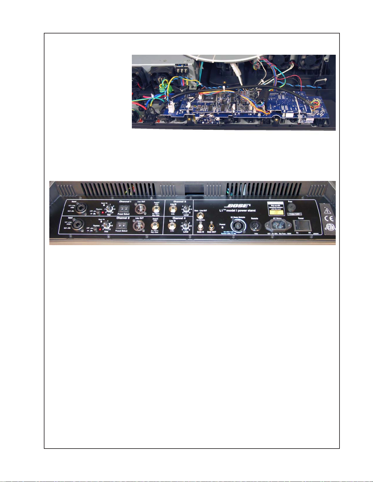
Disassembly Procedures
10. DSP PCB Removal
10.1 Perform proce-
dure 1.
10.2 Make a note of
the wiring configuration
and unplug the six wire
harnesses from the
connectors on the
board.
10.3 Using a pair of
needle-nose pliers, compress the bottoms of the plastic standoff posts used to attach the DSP
PCB to the Input/Output PCB. Lift the DSP PCB off of the I/O PCB.
11. Input/Output PCB Removal
11.1 Perform procedures 9 and 10.
11.2 On the front panel of the power stand, remove the four knobs for the mic trim and level
controls.
11.3 Using a nut driver, remove the nuts and washers for the 1/4 inch phono jacks.
11.4 Using a Phillips-head screwdriver, remove the screws that secure the XLR, Data in/out
and Neutrik connectors to the front panel.
11.5 Lift the I/O PCB off of the input panel.
75
Page 76

Disassembly Procedures
Line Array Procedures
Note: The line arrays are divided into a
lower line array, which plugs directly into the
power stand, and an upper line array, which
uses a bayonet arrangement to align the
upper array to the lower array for connection. All electrical connections are automatically made when the arrays are mounted
into the power stand and the upper array is
mounted to the lower array.
Note: Refer to Figure 8 for the following
procedures.
1. Grille Removal
1.1 Using a Phillips-head screwdriver,
remove the six screws that secure the end
cap to the line array enclosure. Lift off the
end cap. Unplug the molex connector from
the speaker harness.
1.2 Grasp the edge of the grille and gently
lift it away from the enclosure.
2. Nameplate Removal
2.1 Perform procedure 1.
2.2 On the back of the grille, unbend the
legs of the logo. Lift off the nameplate.
4. Upper Line Array Top End Cap Removal
4.1 Using a Phillips-head screwdriver,
remove the seven screws that secure the
end cap to the line array enclosure. Lift off
the end cap.
Re-assembly note: Make sure that the end
cap gasket is properly aligned to achieve an
airtight seal.
5. Upper Line Array Bottom End Cap
Removal
5.1 Using a Phillips-head screwdriver,
remove the seven screws that secure the
end cap to the line array enclosure. Lift the
end cap away from the enclosure. Unplug
the molex connector from the speaker
harness.
Re-assembly note: Make sure that the end
cap gasket is properly aligned to achieve an
airtight seal.
6. Lower Line Array Top End Cap Removal
6.1 Using a Phillips-head screwdriver,
remove the six screws that secure the end
cap to the line array enclosure. Lift off the
end cap. Unplug the molex connector from
the speaker harness.
3. Driver Removal
3.1 Perform procedure 1.
3.2 Using a Phillips-head screwdriver,
remove the four screws that secure the
driver to the enclosure.
3.3 Lift the driver out of the enclosure. Note
the wiring configuration and cut the wires as
close to the driver terminals as possible.
Re-assembly note: Make sure that the end
cap gasket is properly aligned to achieve an
airtight seal.
7. Lower Line Array Bottom End Cap
Removal
7.1 Using a Phillips-head screwdriver,
remove the seven screws that secure the
end cap to the line array enclosure. Lift the
end cap away from the enclosure. Unplug
the molex connector from the speaker
harness.
Re-assembly note: Make sure that the end
cap gasket is properly aligned to achieve an
airtight seal.
76
Page 77

Disassembly Procedures
8. Front Cap Removal
8.1 Using a Phillips-head screwdriver,
remove the four screws that secure the front
cap to the bottom front of the line array
enclosure. Lift the end cap away from the
enclosure.
Bass Module Procedures
Note: Refer to Figure 9 for the following
procedures.
1. Grille Removal
1.1 Using an allen wrench, remove
the four screws that secure the grille to the
upper and lower speaker end caps.
1.2 Lift off the grille.
2. Nameplate Removal
4. Input Panel Removal
4.1 Using a Phillips-head screwdriver,
remove the four screws that secure the
input panel to the bass module enclosure.
4.2 Lift the input panel away from the bass
module enclosure.
4.3 Make a note of the wiring configuration
and un-solder the speaker harness wires
from the input panel.
2.1 Perform procedure 1.
2.2 On the back of the grille, remove the
retaining nut and spring from the post of the
nameplate. Lift the nameplate off of the
grille.
3. Driver Removal
3.1 Perform procedure 1.
3.2 Using a Phillips-head screwdriver,
remove the four screws that secure the
driver to the bass module enclosure.
3.3 Lift the driver out of the enclosure. Note
the wiring configuration and cut the wires as
close to the driver terminals as possible.
Re-assembly notes:
- When soldering the speaker harness wires
to the new driver, be sure to observe polarity
of the driver harness wires.
- Be sure to properly align the gasket behind
the new driver to ensure an airtight fit.
77
Page 78
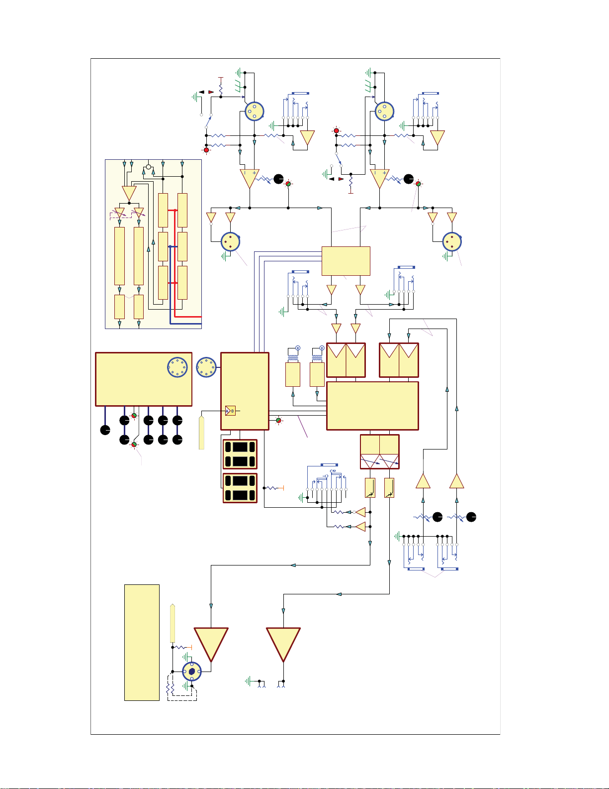
2-Mar-2007
S-DATA Out
(to SPDIF)
Ch 3 In
Ch 4 In
L
R
Master Vol. Range: -80 to +22dB (+10@12:00)
Sys. EQ+X-Over, Hi
Sys. EQ+X-Over, Lo Limiter
Limiter
Knee=+1.5dBV
Bass Out
Hi Out
Remote
Figure 11. L1
+24v
O
PHANTOM
Ch2 In
Ch1 In
DSP Processing Block Diag
-1
User EQ Preset EQNoiseGate
User EQ Preset EQNoiseGate
3
Ch1/2 Preset
Remote
®
Model I Power Stand Block Diagram
Max. Level = +10dBV
Nom. Level = -21dBV(Trim ctr)
Min. Level = -66dBV for full output
Input-LINE
PHANTOM
Control
Ch2 Insert
0dB
Nom. -10dBV
Clip@+6dBV
Data In
(SPDIF)
(Trim, Ch1 Vol+Master @ Max)
Input-MIC
O
+24v
+24
Clip@+18dBV
Volume
Digital
2-Ch.
Max. Gain = 0dB
Nom. Gain = -10dB (12:00)
Min. Gain = -40dB
+1
+1
0dB
+1
+1
0dB
0dB
12
3
INA163
5K 10C
Nom.: 0dBV
TC A9459F
Tip = Return
Nom. -10dBV
Clip@+6dBV
+24
Input-MIC
3
INA163
Ch2 Line Out
+1
12
Clip@+24dBV
Ch2
12
+8 to +50 dB
Mic (XLR) input
+21dB @ ctr
5K 10C
Trim
Nom.: +6dBV (Balanced)
Ring = Send
Tip = Return
-20dB
Line (1/4") input
Sig/OL
(SPDIF)
+1
-12 to +30 dB
+1dB @ ctr
Data-Out
CS5361
Xmiter
S3PC8475
SPDIF
Rcvr
SPDIF
A/D
A/D
CS8416
CS8406
µC
DSP
Ch1
+8 to +50 dB
Mic (XLR) input
+21dB @ ctr
Ring = Send
A/D
A/D
+1
-20dB
-12 to +30 dB
Line (1/4") input
+1dB @ ctr
Sig/OL
Trim
Green=Signal= -30dBV
Red=Clip=+6dBV
-1
3
Ch1 Insert
Nom. -10dBV
Clip@+6dBV
CS5361
ADS21065L
Max. Level = +18dBV [input buer clips]
Nom. Level = -1dBV
Min. Level = -46dBV for full output
Input-LINE
(Ch1 Vol+Master @ Max)
Ch1 Line Out
+1
BLOCK DIAGRAM -
12
Nom.: +6dBV (Balanced)
Clip@+24dBV "
Signal Processing + Routing
Master
Level
Low
Sig/OLSig/OL
Clip= -4dBV into A/D
Signal= -40dBV into A/D
Persistence = 100msec
BASS SPEAKER SENSING:
R=Open: Amp1&2 Wider-Band EQ
R=10K: 40-150Hz X-Over on Bass,
>150Hz-Hi
R=5K: X-Over on Bass Ch, -6dB Hi Range
Mid
Ch1 Ch2
High
250W@4 Ohms
+1dBV (1.1V) for
8/4 ohm Sense
2+
+29dB
+5
1-
2-
8/4 ohm Sense
Ch1 Ch2
PRESET
Power
Amp
Clip @ +30dBV
1+
(250W 4ohms)
0 1
0 1
Amp2
Bass Module
Bass Slave Sense
Amp
+29dB
Power / Protect / Diagnostic
Master Vol Ctrl
+5
5
678
9
Amp1
Power
LineSource
Top+Bottom
432
Bass Send
D/A
LPF
1
-1 +1
-1.5dB
D/A
LPF
CS4392
-1.5dB
+20dB
+2.6dB @ 12:00
Level
20K 15A
Ch 4 IN
Ch 3 IN
Max. Level = +40dBV+
Nom. Level = -13dBV (pot @ ctr)
Min. Level = -30dBV for full output
+20dB
Level
20K 15A
Rev:
A
78
Page 79

Test Procedures
L1® Model I Power Stand Tests
Equipment Required
• dB Meter
• Digital Multi-meter
• Audio Signal Generator
• Distortion Meter
• 2 - 4 Ohm, 250 Watt Load Resistors
• Test cables, see Appendix
Overall System Tests
Notes:
1. Do not connect the R1 remote control for
the following tests, unless specified. Powering up the power stand without the remote
has the same effect as setting all of the
controls on the remote to the midpoint.
2. On the front panel of the power stand, set
the Channel 1 and Channel 2 Preset Select
switches to 00. Short out the 2+ and 2connections on the B1 Bass Module output
connector using the test cable described in
section 1 of the appendix of this manual.
This will put the power stand into debug
mode for the following tests. In this mode the
crossover, the compressor and the EQ are
disabled. The DSP will pass a flat response.
The level controls and the clip indicators still
operate in this mode.
3. Refer to Figure 11, L1 Model I Block
Diagram, for the following procedures.
1. Channel 1 and 2 Mic Input Gain Tests
1.3 Using a balanced XLR male input cable,
apply a 1 kHz, -30dBV signal to the channel
1 input.
1.4 Reference a dB meter to the input level.
Measure the gain at the output of the
powerstand boot cable described above.
It should be +48.5 dB + 3 dB.
1.5 Repeat steps 1.1 to 1.4 for the channel
2 Mic input.
2. Channel 1 and 2 Mic Input Frequency
Response and Distortion Tests
2.1 Connect the powerstand boot test cable
to where the line array would usually sit.
Details on this cable appear in the appendix.
2.2 On the left hand side of the input/output
panel, set the channel 1 Mic Trim control to
the 6 setting. Ensure that the phantom
power push button is not pushed in.
2.3 Using a balanced XLR male input cable,
apply a 1 kHz, -30 dBV signal to the channel
1 input.
2.4 Use an 80kHz low-pass filter on your
measuring equipment. Reference a dB
meter to the input level. Measure the frequency response at the powerstand boot
test cable. It should be 0 dB + 3 dB from
30 Hz to 15 kHz.
1.1 Connect the powerstand boot test cable
to where the line array would usually sit.
Details on this cable appear in the appendix.
1.2 On the left hand side of the input/output
panel, set the channel 1 Mic Trim control to
the 6 setting. Ensure that the Phantom
Power push button is not pushed in.
2.5 Measure the total harmonic distortion
(THD) level at the powerstand boot cable.
It should be 0.25% max at 1 kHz and 1.5%
max at 15 kHz.
2.6 Repeat steps 2.1 to 2.5 for the channel
2 Mic input.
79
Page 80

Test Procedures
3. Channel 1 and 2 Mic Input Signal to
Noise Ratio (Dynamic Range) Tests
3.1 Connect the powerstand boot test cable
to where the line array would usually sit.
Details on this cable appear in the appendix.
3.2 On the left hand side of the input/output
panel, set the channel 1 mic trim control to
the 6 setting. Ensure that the phantom
power push button is not pushed in.
3.3 Using a balanced XLR male input cable,
apply a 1 kHz, -30 dBV signal to the channel
1 input.
3.4 Reference a dB meter to the output level
at the powerstand boot cable. Remove the
input signal and measure the A-Weighted
output level. It should be -80 dB minimum.
3.5 Repeat steps 3.1 to 3.4 for the channel 2
Mic input.
4. Channel 1 and 2 Mic Input Phantom
Power Test
4.1 Plug an XLR connector into the channel
1 Mic input. Do not connect any cables to
the channel 1 or channel 2 Mic inputs.
Power on the unit.
4.2 Press the channel 1 phantom power
switch. Verify that the LED lights. Measure
the DC voltage level across pins 1 and 2 of
the XLR connector. Verify that the DC level
is +24Vdc + 1Vdc relative to pin 1.
4.3 Measure the DC voltage level across
pins 1 and 3 of the XLR connector. Verify
that the DC level is +24Vdc + 1Vdc relative
to pin 1.
5. Channel 1 and 2 Line Input Gain Tests
5.1 Connect the powerstand boot test cable
to where the line array would usually sit.
Details on this connector appear in the
appendix.
5.2 On the left hand side of the input/output
panel, set the channel 1 mic trim control to
the 6 setting. Ensure that the phantom
power push button is not pushed in.
5.3 Using an unbalanced 1/4" phono jack
input cable, apply a 1 kHz, -10 dBV signal
to the channel 1 input.
5.4 Reference a dB meter to the input level.
Measure the gain output at the powerstand
boot connector. It should be +28.5 dB + 4
dB.
5.5 On the signal generator, turn the input
level all the way down. Verify that the channel 1 Signal/OL LED is off. Increase the
signal generator level. Verify that the LED
lights green. Increase the signal level again
and verify that the LED lights red.
Note: You may have to increase the Mic
Trim level on the PS1 channel 1 input as
well to get the LED to light red.
5.5 Repeat steps 5.1 to 5.5 for the channel 2
Line input.
6. Channel 1 and 2 Line Input Frequency
Reponse and Distortion Tests
6.1 Connect the powerstand boot test cable
to where the line array would usually sit.
Details on this connector appear in the
appendix.
4.4 Repeat steps 4.1 to 4.3 for channel 2.
6.2 On the left hand side of the input/output
panel, set the channel 1 Mic Trim control to
the 6 setting. Ensure that the Phantom
Power push button is not pushed in.
6.3 Using an unbalanced 1/4" phono jack
input cable, apply a 1 kHz, -10 dBV signal
to the channel 1 input.
80
Page 81

Test Procedures
6.4 Use an 80 kHz low-pass filter on your
measuring equipment. Reference a dB
meter to the input level. Measure the frequency response at the powerstand boot
connector. It should be 0 dB + 3 dB from
30 Hz to 15 kHz.
6.5 Measure the Total Harmonic Distortion
(THD) level at the powerstand boot connector. It should be 0.25% max at 1 kHz and
1.5% max at 15 kHz.
6.6 Repeat steps 6.1 to 6.5 for the channel 2
Line input.
7. Channel 1 and 2 Line Input Signal to
Noise Ratio (Dynamic Range) Tests
7.1 Connect the powerstand boot test con-
nector to where the line array would usually
sit. Details on this connector appear in the
appendix.
8.3 Reference a dB meter to the input level.
Measure the gain output at the Bass/Amp 3
OUT jack. It should be +40.1 dB + 3 dB.
8.4 Repeat steps 8.1 to 8.3 for the channel
4 Line input.
9. Channel 3 and 4 Line Input Frequency
Response and Distortion Tests
9.1 Connect the powerstand boot test con-
nector to where the line array would usually
sit. Details on this connector appear in the
appendix.
9.2 On the left hand side of the input/output
panel, set the channel 4 trim control to the
6 setting.
9.3 Using an unbalanced 1/4" phono jack
input cable, apply a 1 kHz, -20 dBV signal
to the channel 1 input.
7.2 On the left hand side of the input/output
panel, set the channel 1 Mic Trim control to
the 6 setting. Ensure that the Phantom
Power push button is not pushed in.
7.3 Using an unbalanced 1/4" phono jack
input cable, apply a 1 kHz, -10 dBV signal to
the channel 1 input.
7.4 Reference a dB meter to the output level
at the powerstand boot connector. Remove
the input signal and measure the AWeighted output level. It should be -80 dB
minimum.
7.5 Repeat steps 7.1 to 7.4 for the channel 2
Line input.
8. Channel 3 and 4 Line Input Gain Tests
8.1 On the left hand side of the input/output
panel, set the channel 3 Level control to the
6 setting.
8.2 Using an unbalanced 1/4" phono jack
input cable, apply a 1 kHz, -20 dBV signal to
the channel 1 input.
9.4 Use an 80 kHz low-pass filter on your
measuring equipment. Reference a dB
meter to the input level. Measure the frequency response at the powerstand boot
connector. It should be 0 dB + 3 dB from
30 Hz to 15 kHz.
9.5 Measure the Total Harmonic Distortion
(THD) level at the powerstand boot connector. It should be 0.25% max at 1 kHz and
1.5% max at 15 kHz.
9.6 Repeat steps 9.1 to 9.5 for the channel
4 Line input.
10. Channel 3 and 4 Line Input Signal to
Noise Ratio (Dynamic Range) Tests
10.1 On the left hand side of the input/
output panel, set the channel 3 Level
control to the 6 setting.
10.2 Using an unbalanced 1/4" phono jack
input cable, apply a 1 kHz, -10 dBV signal to
the channel 1 input.
81
Page 82

Test Procedures
10.3 Reference a dB meter to the output
level at the Bass/Amp 3 OUT jack. Remove
the input signal and measure the AWeighted output level. It should be -80 dB
minimum.
10.4 Repeat steps 10.1 to 10.3 for the
channel 4 Line input.
11. Channel 1 and 2 Remote Control,
Preset Switch and Insert Function Tests
11.1 Connect the power stand to a known
good L1 model I line array. Set the channel 1
preset switch to 00. Connect the remote
control to the unit using the remote control
MIDI cable supplied with the power stand.
11.2 Connect an analog audio source to the
Channel 1 line input 1/4 inch jack. This
source can be a CD player with a music
disc.
11.3 Adjust the trim level so that the LED is
lit mostly green. The audio should sound
normal.
11.4 With the audio playing, change the
channel 1 preset to 97 and back to 00. The
channel should mute gracefully when the
preset switch is operated. The audio should
fade back in again about a second after the
switch has stopped operating.
Note: Preset 97 is a 1 kHz band pass
(telephone-type sound). Preset 00 should
sound normal.
11.5 Operate all channel 1 controls on the
remote (high, mid, low, volume and master
volume). All tone controls should have a
clearly audible effect and operate smoothly.
Channel volume may display a little “zipper”
noise, which is normal.
Note: Channel volume all the way down
does not mute the channel, but the output
level should be very low. There is a small,
but noticeable time delay between operating
the control and the audible effect. This is
normal. The master volume control should
operate smoothly without any artifacts.
11.6 Insert a 1/4 inch phono jack all the way
into the channel 1 Insert jack. The audio
should sound normal.
11.7 Insert a 1/4 inch phono jack into the
channel 3 Line IN jack and operate the
volume control on the power stand. The
audio should sound normal.
11.8 Repeat steps 11.1 to 11.7 for the channel 2 input.
12. Channel 1 Send, Line Output and
Digital Output Tests
Note: For these tests you will need an
external device that can accept both 1/4
inch and XLR inputs. A small mixer, such
as a Mackie or Behringer with headphones
connected works well for this. The master
volume control on the remote control should
be set all the way down to mute all sound
coming from the unit under test.
12.1 Connect the power stand to a known
good L1 model I line array. Set the channel
1 preset switch to 00. Connect the remote
control to the unit using the remote control
MIDI cable supplied with the power stand.
12.2 Connect an analog audio source to the
Channel 1 Line IN 1/4 inch jack. This source
can be a CD player with a music disc.
12.3 Adjust the trim level so that the LED is
lit mostly green. The audio should sound
normal.
12.4 Insert a 1/4 inch plug halfway into the
channel 1 Insert jack. The audio should
sound normal.
12.5 Connect the power stand channel 1
XLR Line OUT jack to the XLR input of the
mixer. The audio should sound normal.
Note: The power stand puts out a “professional” +4dBu level. You may have to turn
the the input trim control on the mixer all the
way down to prevent overloading the signal
and distorting it.
82
Page 83

Test Procedures
12.6 Connect the Data Out jack of the PS1 to
a device that accepts a 48 kHz S/PDIF data
stream. The audio should sound normal.
13. Power Amplifier Tests
13.1 Connect the power stand to a known
good L1 model I line array. Set the channel 1
preset switch to 00. Connect the remote
control to the unit using the remote control
MIDI cable supplied with the PS1.
13.2 Connect an analog audio source to the
Channel 3 IN 1/4 inch phono jack. This
source can be a CD player with a music
disc.
13.3 Verify that audio comes from the L1
model I line array. The audio should sound
clean and undistorted.
13.4 Verify that audio comes from the B1
bass module. The bass should be clean and
undistorted.
15. Bass Module Auto-EQ Test
15.1 Connect a L1 line array to the power
stand. Connect an R1 remote control to the
power stand. Connect a B1 bass module to
the B1 Bass Module output jack on the
power stand. Connect an audio source to
the channel 1 and 2 inputs of the power
stand.
15.2 Set the channel 1 and 2 level controls
to identical settings so that both LEDs are
mainly green.
15.3 While the audio is playing, disconnect
the B1 bass module from the power stand.
The system should mute and un-mute and
audio should resume. The audio should
sound normal, but not punchy (no deep
bass).
15.4 Plug a dummy 1/4 inch phono jack into
the Bass Line Out jack. The system should
mute and un-mute again, but the audio
should sound thinner than before.
14. High SPL System Sweep Test
CAUTION: This test will be extremely loud.
Hearing protection is advised.
14.1 Connect a R1 remote control to the
power stand under test. Set the channel 1
controls to mid-level. Set the master volume
control on the remote to the 1 o’clock position. Set the channel 1 Mic Trim control on
the PS1 to 6. Connect a L1 model I line
array to the PS1. Connect a B1 bass module
to the PS1.
14.2 Connect a signal generator to the
channel 1 input on the PS1. Adjust the
signal generator and/or trim control so that
the Signal/OL LED is just below red.
14.3 Sweep the input frequency from 40 Hz
to 14 kHz. Listen for any unusual noises and
excessive distortion or drop-outs.
15.5 Remove the dummy plug. The system
should mute and un-mute and the audio
should sound normal again.
15.6 Re-connect the B1 bass module to the
power stand. The audio should mute and unmute again and sound normal.
15.7 Connect a second B1 bass module to
the first one. The audio should mute and unmute. The audio will sound very similar to
having only one bass module attached.
Disconnect the second bass module. The
system should mute and un-mute and the
audio should sound normal again.
83
Page 84

Test Procedures
L1® Model I Line Array Tests
Set up the unit under test as shown below.
Upper or Lower
L1 Line Array
Audio Signal
Generator
Power Amplifier
INPUT OUTPUT
Upper or Lower L1
Line Array Test Cable
Note: To distinguish between normal suspension noise and rubs or ticks, displace the
cone slightly with your fingers. If the noise
stays the same, it is normal suspension
noise and the driver is good. Suspension
noise will not be heard with program material.
3. Transducer Phase Test
3.1 Apply a DC voltage of 10V, positive
applied to the positive tab of the dual
banana jack on the line array test cable and
negative applied to negative (gnd) tab.
3.2 All of the driver cones should move
outward when the DC voltage is applied.
3.3 Rewire any incorrectly connected transducers.
4. L1 Model I Line Array Sweep Test
1. Air Leak Test
1.1 Apply a 100 Hz, 10 Vrms sine wave to
the unit under test.
1.2 Listen carefully for air leaks from around
the end cap, the transducers and the grille.
Air leaks will be heard as a hissing or sputtering sound. All repairs must be hidden.
Test duration should be 5 seconds minimum.
2. Transducer Rub and Tick Test
2.1 Remove the transducer you wish to test
using the disassembly procedures in this
manual. Do not unplug the wires at the
transducer assembly terminals.
2.2 Connect a signal generator directly to
the terminals of the transducer assembly
under test.
4.1 Set up the upper or lower line array
section as shown in the figure on the previous page.
4.2 Apply a 100 Hz, 10 Vrms sine wave to
the input.
4.3 While listening to the output of the
system, sweep the input frequency slowly
from 100 Hz to 15 kHz.
4.4 Listen carefully for any extraneous
noises such as buzzing and ticking.
2.3 Apply a 20 Hz, 5 Vrms signal to the
transducer assembly.
2.4 Listen carefully for any extraneous
noises such as rubbing, scraping or ticking.
84
Page 85
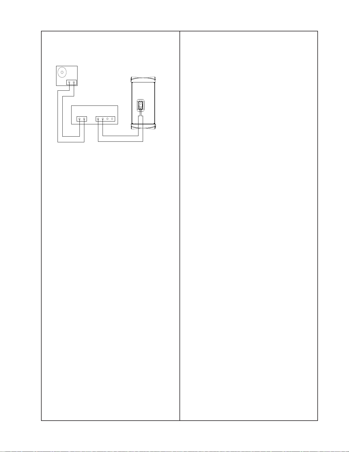
Test Procedures
B1 Bass Module Tests
Set up the unit under test as shown below.
Audio Signal
Generator
B1 Bass Module
Power Amplifier
INPUT OUTPUT
B1 Bass Module
Test Cable
1. Air Leak Test
1.1 Apply a 100 Hz, 20 Vrms sine wave to
the unit under test.
1.2 Listen carefully for air leaks from around
the end cap, the transducers and the grille.
Air leaks will be heard as a hissing or sputtering sound. All repairs must be hidden.
Test duration should be 5 seconds minimum.
3. Transducer Phase Test
3.1 Apply a DC voltage of 20V, positive
applied to the positive tab of the dual
banana jack on the bass module test cable
and negative applied to negative (gnd) tab.
3.2 Notice carefully that all driver cones
should move outward when the DC voltage
is applied.
3.3 Rewire any incorrectly connected transducers.
4. System Sweep Test
4.1 Set up the system as shown in the
figure at left.
4.2 Apply a 10 Hz, 20 Vrms sine wave to the
input.
4.3 While listening to the output of the
system, sweep the input frequency slowly
from 10 Hz to 400 Hz.
2. Transducer Rub and Tick Test
2.1 Remove the transducer you wish to test
using the disassembly procedures in this
manual. Do not unplug the wires at the
transducer assembly terminals.
2.2 Connect a signal generator directly to
the terminals of the transducer assembly
under test.
2.3 Apply a 10 Hz, 10 Vrms signal to the
transducer assembly.
2.4 Listen carefully for any extraneous
noises such as rubbing, scraping or ticking.
Note: To distinguish between normal suspension noise and rubs or ticks, displace the
cone slightly with your fingers. If the noise
stays the same, it is normal suspension
noise and the driver is good. Suspension
noise will not be heard with program material.
4.4 Listen carefully for any extraneous
noises such as buzzing and ticking.
85
Page 86
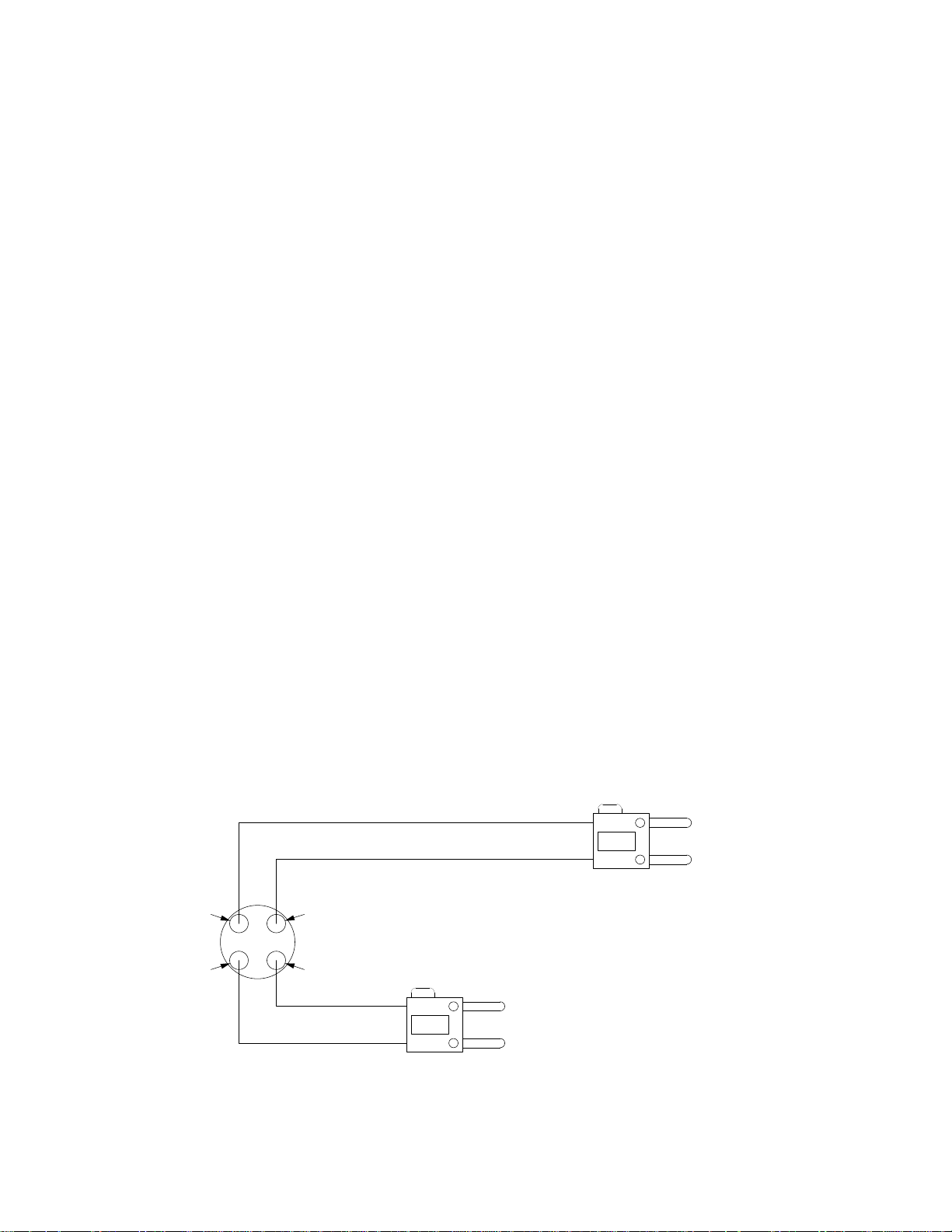
Appendix
L1® Model I Power Stand Test Cables
Note: In order to be able to properly test the L1 Model I Power Stand, you will need to make a
few test cables.
1. Amplifier Output Test Cable:
Parts needed:
®
1- Neutrik
Speakon® NL4FX Speakon X-Line/4 Pole connector.
4 - Dual banana jacks
2 - 10k ohm, 1/4 Watt resistors
16 or 18 AWG twisted pair wire, 6 feet
18 AWG twisted pair wire, 2 feet
This cable is used to connect the B1 Bass Module output jack to the load resistors used in the
test procedures. The connector used is a Neutrik NL4FX Speakon X-Line / 4 Pole type. This
connector has 4 terminals labeled 1+, 1-, 2+ and 2-. Terminals 1+ and 1- are used to connect to
the load resistors. Use 18 or 16 AWG wire for these terminals. Use twisted pair wires to avoid
inducing noise into the cable during use.
The 2+ and 2- terminals will be used to sense the loads connected to the Speakon connector
when used with the B1 Bass Module jack. This jack automatically senses the load on this jack to
properly tailor the EQ and output level for the connection of one or two bass modules. It does
this by sensing the resistive value across terminals 2+ and 2-. The bass modules have a 10k
ohm resistor across these terminals. When only one bass module is connected, the power
stand sees the 10k resistance and sets the EQ and output level accordingly. When two bass
modules are connected, it sees 5k and sets the EQ and output level accordingly. For the test
cable, you will use 18 AWG twisted pair wire to a dual banana jack.
It is also useful to have 3 spare banana jacks, one with a short across it and 2 with a 10k Ohm,
1/4 Watt resistor each to simulate a bass module connected to the terminals.
GND
Amplifier output
to load resistor
16-18AWG twisted pair wire
1+1-
Neutrik Speakon
4 pole connector
(back shown)
2-2+
18AWG twisted pair wire
Dual banana jack
Dual banana jack
GND
Bass module
sensing output
Figure 12. Amplifier Output Test Cable Wiring Diagram
86
Page 87

Appendix
TIP RING SLEEVE
2. Powerstand Boot Test Cable
1 - 10 pin Molex female connector, Molex part number 39-01-3103
4 - Molex crimp-on pins for above connector
1 - dual banana jack
12 feet of 16 or 18AWG twisted pair wire
Cut the 12 foot length of twisted pair wire in half. Strip all of the wires back about 1/4 inch.
Crimp the molex pins onto the wires. The positive (+) side of the twisted pair wires will go into
pins 3 and 8 of the Molex connector. The negative (-) side of the twisted pair wires will go into
pins 4 and 9 of the Molex connector. Connect the wires that go to pins 3 and 8 of the Molex
connector to the positive (+) side of the dual banana jack. Connect the wires that go to pins 4
and 9 of the Molex connector to the negative (-) side of the dual banana jack.
This test cable plugs into the boot connector of the L1TM Model I Power Stand for all line array
amplifier tests.
3. XLR Microphone Input Test Cable
Parts needed:
1 - XLR male connector
1 - Dual banana jack
18 AWG shielded twisted pair wire, 6 feet
This cable is used to test the channel 1 and 2 microphone inputs on the power stand. These
input jacks are dual purpose jacks that will accept either XLR or 1/4" TRS phono jack balanced
inputs.
Connect the dual banana jack’s positive (+) connection to pin 2 of the XLR jack. Connect the
dual banana jack negative (-) connection to pin 3 of the XLR jack. Connect the cable shield to
pin 1 of the XLR jack.
4. Line Input 1/4" Phono Jack Test Cable
Parts needed:
1 - Mono 1/4" phono jack
1 - Dual banana jack
18 AWG shielded twisted pair wire, 6 feet
This cable is used to test the channel 1 and
2 line inputs on the power stand.
Connect the dual banana jack’s positive (+) connection to the tip connection of the 1/4" phono
jack. Connect the dual banana jack negative (-) connection to the ring connection of the 1/4"
phono jack.
87
Page 88

Appendix
5. Insert Jack Test Cable
This cable is used to test the channel 1 and 2 insert jacks on the power stand. When you plug it
into the channel 1 or channel 2 insert jack, you will be able to separate the sections of the
electronics. Refer to the power stand block diagram on page 71. The RETURN dual banana
jack will give you the output of the circuitry up to the output of the 2 channel digital volume
control. The SEND dual banana jack will allow you to input a signal to test the circuitry after the
insert jack, which is the input to the A/D converter and DSP.
Parts needed:
1 - Tip/Ring/Sleeve (stereo) 1/4" phono jack
2 - Dual banana jacks
Shielded stereo cable, 6 feet
For each of the shielded stereo pairs of wires, connect the dual banana jack’s positive (+)
connection to the center conductor. Connect the dual banana jack’s negative (-) connection to
the shield wires. Use an Ohmmeter to determine which of the center conductors is connected to
the ring of the 1/4 inch TRS phono jack. Using a permanent black magic marker, label this dual
banana connector SEND. Determine which of the center conductors is connected to the tip of
the 1/4 inch TRS phono jack. Label this dual banana connector RETURN. The sleeve portion of
the jack is the common ground where the shields are connected.
6. L1® Model I Line Array Test Cables
These two cables will allow you to test the upper and lower line array sections without an L1
Model I power stand. Use these cables for the line array test procedures in this service manual.
Lower Line Array Section Test Cable
Parts needed:
1 - 10 pin Molex male connector, Molex part number 39-00-0039 (F)
4 - Molex crimp-on pins for above connector, Molex part number 39-00-0039
1 - dual banana jack
12 feet of 16 or 18AWG twisted pair wire
Cut the 12 foot length of twisted pair wire in half. Strip all of the
wires back about 1/4 inch. Crimp the molex pins onto the wires.
The positive (+) side of the twisted pair wires will go into pins 3
and 8 of the Molex connector. The negative (-) side of the twisted
pair wires will go into pins 4 and 9 of the Molex connector. Connect the wires that go to pins 3 and 8 of the Molex connector to
the positive (+) side of the dual banana jack. Connect the wires
that go to pins 4 and 9 of the Molex connector to the negative (-)
side of the dual banana jack.
123 54
678910
Molex Connector Rear View
88
Page 89
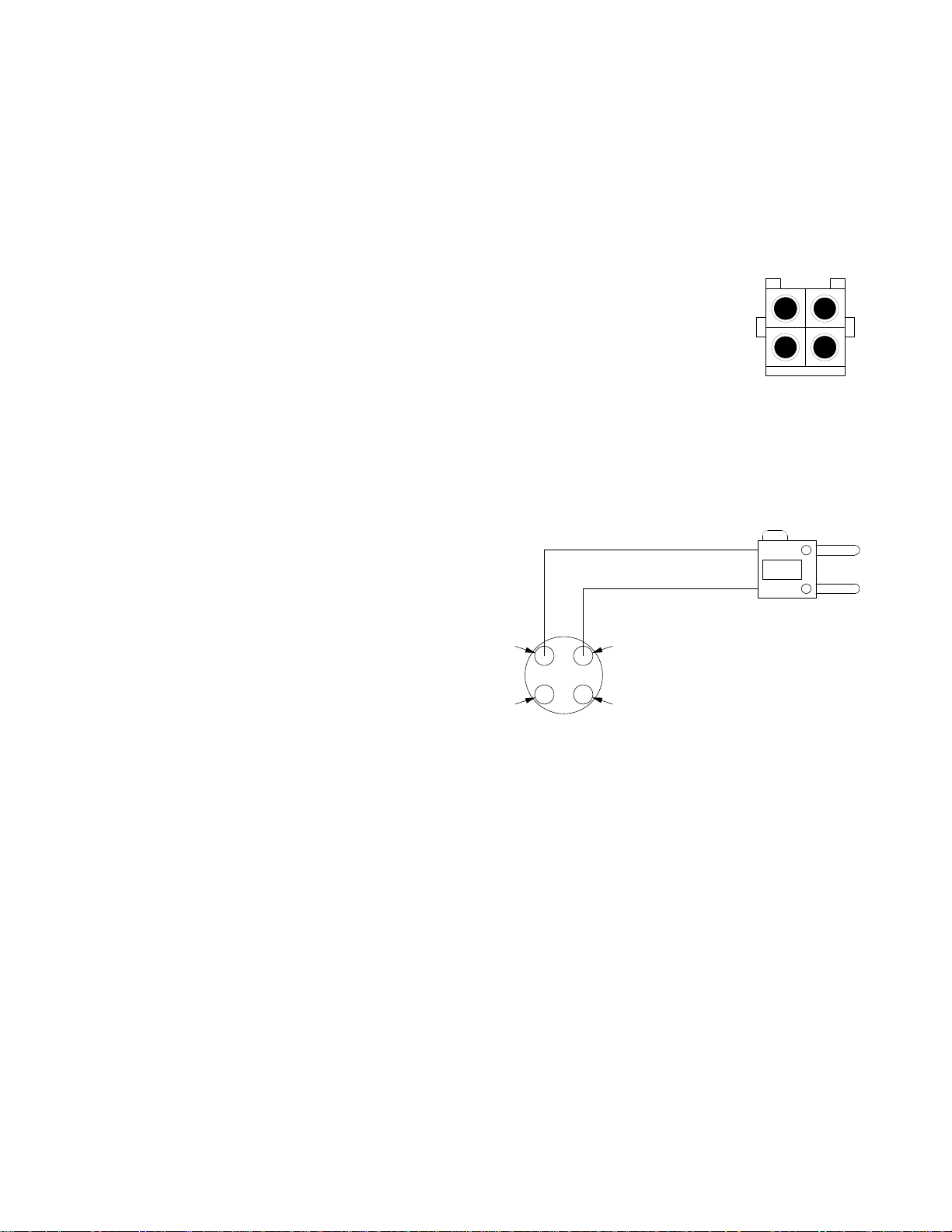
Appendix
Upper Line Array Section Test Cable
Parts needed:
1 - 4 pin Molex male connector, Molex part number 39-01-2041
4 - Molex crimp-on pins for above connector, Molex part number 39-00-0041 (M)
1 - dual banana jack
12 feet of 16 or 18AWG twisted pair wire
Cut the 12 foot length of twisted pair wire in half. Strip all of the wires back
about 1/4 inch. Crimp the molex pins onto the wires. The positive (+) side of
the twisted pair wires will go into pins 2 and 4 of the Molex connector. The
negative (-) side of the twisted pair wires will go into pins 1 and 3 of the
Molex connector. Connect the wires that go to pins 2 and 4 of the Molex
connector to the positive (+) side of the dual banana jack. Connect the wires
that go to pins 1 and 3 of the Molex connector to the negative (-) side of the
dual banana jack.
6. Bass Module Test Cable
Parts needed:
1 - Neutrik® Speakon® NL4FX connector
Bass Module Test Cable
1 - dual banana jack
6 feet of 16 or 18AWG twisted pair wire
16-18AWG twisted pair wire
Strip all of the wires back about 1/4 inch.
Connect the dual banana jack’s positive (+)
connection to the 1+ connection of the
Speakon connector. Connect the dual
banana jack negative (-) connection to the
1- connection of the Speakon connector.
1+1-
Neutrik Speakon
4 pole connector
(back shown)
2-2+
34
12
Molex Connector
Rear View
GND
Dual banana jack
89
Page 90

Appendix
L1® Model I Power Stand Software Update Procedure
Required Equipment:
1- CD player with a S/PDIF digital output (do not use a Bose
1- L1 Model I Power Stand update CD (see the instructions for creating this disc below)
1- S/PDIF video cable, part number 183200, or an audio cable with RCA connectors
1- L1 Model I Power Stand AC line cord
L1 Model I Power Stand Update CD Procedure:
®
Lifestyle® media center)
• Go to the Bose Technical Service web page at http://intranet.bose.com/tsg (Bose internal
repair centers) or http:serviceops.bose.com (external Bose affiliated repair centers).
• Navigate to the L1 Model I web page. The link to it is located on the Pro Products web page.
• Scroll down the page until you see the table that the link to the L1 Model I Power Stand soft-
ware update is located in. Download the file to your computer’s desktop.
• Using a CD burner and your CD burner software, burn the file onto a blank CD-R or CD-RW
disc. Once this disc is successfully created, label the disc with the revision of the software.
Update Procedure:
• Plug the CD player into an AC mains outlet.
• Connect the S/PDIF cable to the Audio Outputs/Digital jack on the back of the CD player.
• Connect the other end of the S/PDIF cable to the DATA IN jack on the Power Stand’s input
panel. This jack is located in the middle of the panel. It’s an RCA jack with a white center.
• Connect the Power Stand’s AC line cord to the AC mains jack on the input panel. This jack is
located on the right side next to the power switch.
• Connect the other end of the AC line cord to an AC mains outlet.
• Power up the Power Stand by moving the power switch to the ON position. Wait for the
power LED to light steady green.
• Load the update CD into the CD player. Press the PLAY CD/DVD button on the remote
control. The update process should begin.
• Wait about 5 seconds while the disc is playing. The green power LED on the Power Stand
should blink rapidly, about 10 times per second. After about 10 seconds, the LED should begin
to blink slower, about twice a second.
• The update process is complete. Power down the Power Stand. Disconnect the S/PDIF
cable from the DATA IN jack.
• Verify proper operation of the Power Stand using the test procedures in this service
manual before returning the unit to the customer.
Troubleshooting:
Problems with this update procedure are indicated by the Power Stand’s power LED.
Typical indicators are:
• LED stays a steady green.
• LED blinks slowly red
In either case, simply repeat the process above. Make sure you wait 5 seconds after power
up of the Power Stand before playing the update disc. Ensure all of the cables are properly
connected.
90
Page 91

Theory of Operation
®
1. L1
Model I Power Stand
1.1 Overview
The L1 Model I System is essentially a Natural Amplification sound system, with the following
components:
L1 Model I Power stand, two L1 Model I Cylindrical Radiator® line array sections, R1 remote
control, B1 bass module, AC power cord, remote control cable and bass module loudspeaker
cable (see below). Note: The B1 bass module is an optional component.
R1 remote
control
PS1 power stand
Remote
control cable
AC power cord
B1 bass module 4-wire cable (blue)
Upper and Lower L1 Cylindrical
Radiator™ loudspeaker
B1 bass module
L1 Model I System Components
Changes from the Personalized Amplification System
The L1 Model I power stand is essentially a RoHS compliant update of the Personalized
Amplifcation System. The unit remains functionally unchanged except for a few key points:
1. The line array is now powered by one 250W amplifier instead of two, as on the PAS power
stand. The two line array sections are now wired in parallel and powered by a single amplifier.
They are each 8 ohms, wired in parallel, for a total of 4 ohms in operation. Due to optimization
of the speaker to the amplifier, the output level is virtually the same as the Personalized Amplification System power stand. There is a mechanical stop in the power stand cavity to prevent
users from plugging a PAS line array into an L1 Model I power stand. Users can, however, insert
an L1 Model I line array into a PAS power stand. This will not harm the unit, but will result is a
few dB of loss in output.
2. All ‘Auxiliary’ speaker connectors on the power stand input panel have been removed.
These connectors were originally used intended for users to access the power stand amplifiers
in a stand-alone fashion. They were rarely used and were removed from the L1 Model I power
stand.
91
Page 92

Theory of Operation
Features
The system has the following features:
• All signal processing performed with DSP
• Remote control
• The ability to receive analog signal input and SPDIF digital signal input
• The ability to output analog signal and SPDIF digital signal.
• Channel volume control
• Master volume control
• Mixer
• Tone control
• 100 sets of parameter equalizer
• System equalizer for compensating speaker characteristic
• Noisegate
• Limiter
• Clip indicator
• DSP software update and 100 sets of preset coefficients update
• Power protection and amplification protection
The system delivers 250W of output power for each of the two amplifiers housed in the power
stand. The system uses a 110V / 230V AC power supply, and has a 1M ohm input impedance at
the audio Ch1/Ch2 line input connector and 1.25k ohm input impedance at the audio Ch1/Ch2
MIC connector. Input signal headroom is 2.1Vrms max. A user could operate the system from
the input panel and the remote (refer to figures below).
Power stand Input and Output Connections
92
Page 93
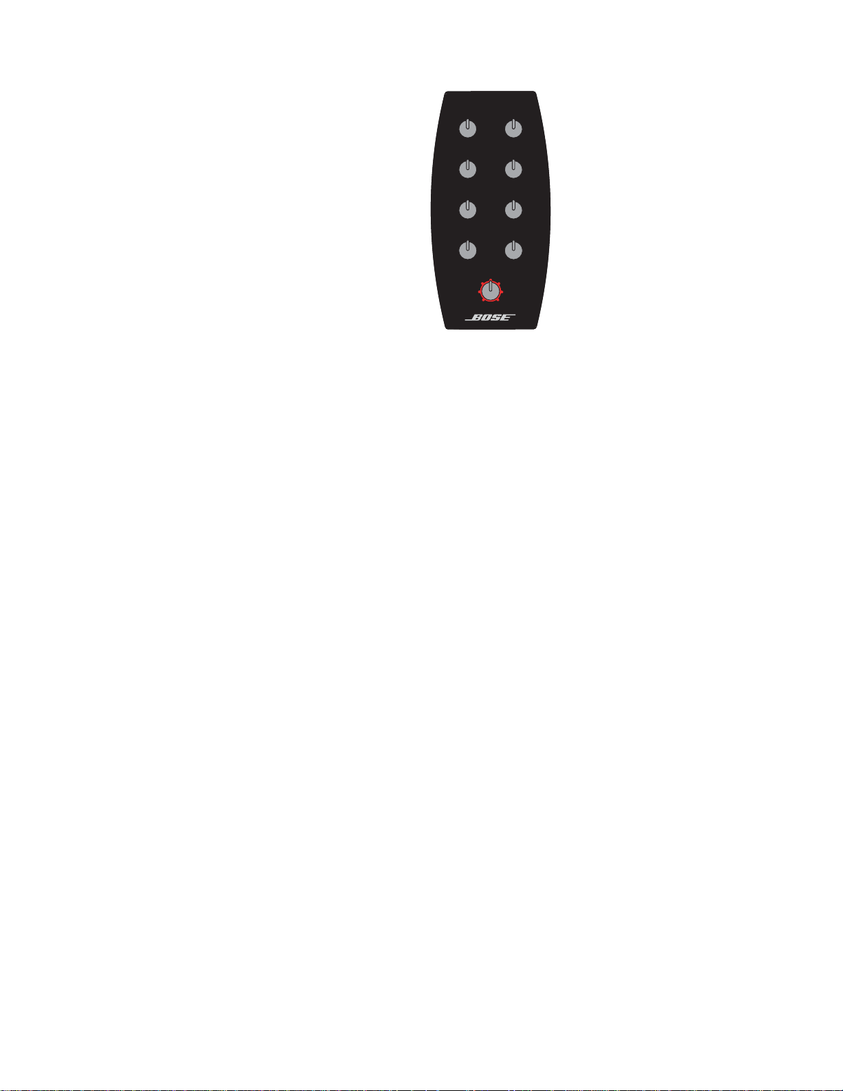
Theory of Operation
0
0
HIGH
MID
LOW
LEVEL
MASTER
0 12
CH2
00
0
-12 +12
0
0 12
SIG / OLSIG / OL
CH1
-12 +12 -12 +12
-12 +12
-12 +12 -12 +12
0 12
R1 remote control
Note: Refer to L1® Model I power stand schematic sheets later in this service manual for the
following information. The information inside the brackets [ ] is the component’s grid location on
the schematic sheet.
The power stand combines the traditional functions of a mixer, digital controller (system EQ and
limiter), power amplifier and mechanical speaker stand. The power stand block diagram (figure
11 on page 71) shows the signal flow through the power stand.
The power stand contains eight PCB assemblies: an EMI (FCC) Filter PCB, two +/-27VDC
switching power supply PCBs, and Auxiliary Power Supply PCB, 2 channels of amplification on
a common PCB, an input panel PCB, DSP PCB, and MCU PCB.
Signal Routing
The power supply connects to the MCU PCB via a the 8 pin connector CN409 [microprocessor
PCB sheet 2, A1], four channels of analog inputs on the panel are connected to the DSP PCB
via a 6 pin connector CN104 [DSP PCB sheet 1, B1], analog output signals on the DSP panel
are connected to input panel via a 3 pin connector CN115 [input panel PCB sheet 2, D1]. SPDIF
IN on the input panel is connected to the DSP PCB via a 2 pin connector CN112 [DSP PCB
sheet 2, B4], SPDIF OUT on the DSP PCB is connected to input panel via a 2 pin connector
CN113 [DSP PCB sheet 2, C8].
For Channel 1 or 2 the signal is input either through the balanced XLR connector or through the
¼” unbalanced connector. The ¼” connector has a very high impedance (900k ohms) to allow
direct connection of passive guitars or bass guitars. The signal is then amplified by the adjustable pre-amplifier. After the pre-amplifier, the signal can be accessed at the balanced XLR line
level output.
Next the signal is routed through a digitally controlled analog volume control. Then, the signal is
routed through the insert loop connector. If there is no plug in the insert jack, the signal will be
routed through. Otherwise the signal will be routed to the “ring” of the connector and is expected
to return from the “tip”. The signal is then digitized in the A/D converters and processed in
software.
93
Page 94

Theory of Operation
t
Software provides the following functions
• Channel 1&2: measuring level for LED
• Channel 1&2: noise gate
• Channel 1&2: preset EQ
• Channel 1&2: channel volume
• Sum channels 1 to 4
• Master Volume Control
• System EQ and crossover (for L1 and B1)
• Limiter & soft clipper (for L1 and B1 amplifiers)
Signal Processing
Signal processing is mainly implemented by the DSP and includes the following functions:
• Noisegate & limiter
• Tone control & volume control
• Parameter equalize & System equalizer
• Clip calculate
The signal flow chart is as follows (refer to the block diagram below):
Ch1 In
Ch2 In
S-DATA Out
(to SPDIF)
Ch 3 In
Ch 4 In
Remote
Ch1/2 Preset
DSP Processing Block Diag
User EQ Preset EQNoiseGate
User EQ Preset EQNoiseGate
L
R
Sys. EQ+X-Over, Hi
Sys. EQ+X-Over, Lo Limiter
Master Vol. Range: -80 to +22dB (+10 @ 12:00)
DSP Functional Block Diagram
Limiter
Knee=+1.5dBV
Hi Out
Bass Ou
94
Page 95

Theory of Operation
Power supplies
To ensure that the system operates normally, the system must be supplied with seven different
voltage levels, +3.3V, +5V, +15V, -15V, +24V, +27V, and -27V. Refer to the block diagram below.
DC Power Supply Block Diagram
110V AC is changed to about 300V DC, after passing through the EMI filter and the diode
bridge. Then, the voltage signal is divided two ways: one DC voltage goes through the switch
control & auxiliary circuit1 again, enters into the transformer primary1. The transformer1 has five
secondary windings, the first outputs +24V DC (for the input panel), the second outputs +15V
DC (for A/D, D/A buffer circuit), the third outputs –15V DC (for A/D, D/A buffer circuit), the fourth
outputs +5V DC (for MCU and other ICs), the fifth outputs +3.3V DC (for DSP, A/D & D/A IC).
Another DC voltage goes through the switch control & auxiliary circuit2 and enters into transformer primary2. The transformer1 has two secondary, the first outputs -27V DC (for AMP), the
second outputs +27V DC (for AMP).
Operation of the all voltage switching regulator is more complicated. The load of +3.3V is the
heaviest, so we get this +3.3V as feedback a signal and send it to the switch control & auxiliary
circuit1. When the system works, if +3.3V happens to waver, switch control & auxiliary circuit1
will change ‘open’ and ‘close’ time of switch circuit to regulate the transformer primary1, accordingly, the voltage of transformer1 secondary will keep stable. Of course, in this way, the effect of
stabilization for +3.3V is best, and that for other voltage is worse.
95
Page 96

Theory of Operation
The regulation of the power supply for AMP is like this: we get the +27V as feedback signal and
send it to switch control & auxiliary circuit2. When system works, if +27V happens to waver,
switch control & auxiliary circuit2 will change ‘open’ and ‘close’ time of switch circuit to regulate
the transformer primary2, accordingly, the voltage of transformer2 secondary will keep stable.
When the system works, +5V can supply 100mA to MCU PCB, +3.3V can supply 260mA to DSP
PCB, +15V can supply 200mA to DSP PCB, -15V can supply 150mA to DSP PCB, and the
+24V can supply 50mA to the Input Panel PCB.
Microcontroller
A microcontroller on the MCU PCB is used for the following control functions:
• Relay DSP information to Remote
• Relay Remote information to DSP
• Control channel volume IC
• Check channel preset switch
• Check bass send state
• Check power & amplification protection
• Check the number of bass speakers connected to the power stand
• Indicate current system working status with a three color LED
These functions are explained in detail on the next page.
Relay DSP information to Remote
The DSP needs to transfer the clip state, channel volume data (cause the table for channel
volume in the DSP), and the system working status to the MCU. The communication adopts
software simulation UART, with two I/O pins as RX and TX. The communication rate is 4800bps,
add a start bit and stop, so every sending byte has 10 bits. Data is sent according to frame
format: frame head | every data | check sum. DSP will transfer a frame every 100ms, and every
sending will take about 15ms.
The MCU needs to transfer the clip state to the Remote. The communication adopts hardware
UART. Communication rate is 9600bps, Data is sent according to the MIDI protocol: MIDI
channel number | MIDI parameter type | MIDI parameter value. The DSP will transfer a frame
data every 100ms, and every sending will take about 3.5ms.
Relay Remote information to DSP
The remote needs to transfer the Ch1EQHi, Ch2EQHi, Ch1EQMi, Ch2EQMi, Ch1EQLo,
Ch2EQLo, Ch1Volume, Ch1Volume, and the MasterVolume to MCU. The communication
adopts hardware UART. Communication rate is 9600bps, Data is send according to MIDI protocol: MIDI channel number | MIDI parameter type | MIDI parameter value. DSP will transfer a
frame data every 100ms, and every sending will take about 30ms.
The MCU needs to transfer the Ch1EQHi, Ch2EQHi, Ch1EQMi, Ch2EQMi, Ch1EQLo,
Ch2EQLo, Ch1Volume, Ch1Volume, MasterVolume, Ch1Preset, Ch2Preset, BassChk, and the
CheckSum to the DSP. The communication adopts software simulation UART, with two I/O pin
as RX and TX. Communication rate is 4800bps, add start bit and stop, so every sending byte
has 10 bits. Data is send according to frame format: every data | check sum. DSP will transfer a
frame every 100ms, and every sending will take about 30ms.
96
Page 97

Theory of Operation
Control channel volume IC
Because the design requires that the channel signal could change from –40dB to 0dB, we use a
volume control IC. There are three pins used to control the volume control IC: CLK, DATA, STB.
CLK, DATA and the STB time sequence is implemented by software.
Check channel preset switch
In the audio processing, there is a parameter equalizer, and the system supplies 100 sets of
coefficients for this function. A user could choose a different coefficient to get different sound
effects. This channel preset switch is a user interface to provide the function for choosing a
different coefficient.
Check bass send state
There is a bass-line out plug on the input panel. Through this plug, the system can connect to
one or more Bose® PackLite® Model A1 amplifiers to drive additional bass modules. The bass
send state only has two logic states “0” or “1”, indicating unconnected and connected. Different
states will choose different coefficients for the limiter and the system equalizer.
Check power & amplification protection
When the power supply and amplification have a problem, the system will indicate this to the
user by an LED on the input panel. The power & amplification protection signal also only has
two logic states “0” or “1”, indicating unprotected and protected.
Bass module sensing circuitry
On the bass connector, there are four pins. 1+ and 1- outputs bass signal, 2+ and 2- is used to
check the number of bass modules connected to the power stand. When there is no bass
module connected, the resistance value between 2+ and 2- is greater than 10k ohms, when one
bass module is connected to the power stand, the resistance between 2+ and 2- is equal to 10k
ohms, when two bass modules are connected, the resistance value between 2+ and 2- is equal
to 5k ohms, when there are more than two bass loudspeakers, the resistance value between 2+
and 2- is less than 5k ohms. Once the system detects how many, if any bass modules are
connected to the power stand, it will adjust the output level and the EQ accordingly to provide
the proper outputs for that configuration.
System Status LED
On the input panel PCB, there is a three color LED. The different colors of this LED represent
different operating conditions for the power stand.
• Green: operating normally
• Green blink fast: updating software or preset
• Green blink slowly: software update success
• Red blink slowly: software update failure
• Orange: power or amplification protection enabled (fault condition)
97
Page 98

Theory of Operation
Codec
In the system, there are five codec ICs: U386 (for Ch1 & Ch2 A/D), U385 (for Ch3 & Ch4 A/D),
U387 (for line & bass D/A) [DSP PCB sheet 1, B/C/D5], U431 (for SPDIF IN) [DSP PCB sheet 2,
D3], U435 (for SPDIF OUT) [DSP PCB sheet 2, B6].
U386, U385, U387, U431, and U435 include the following functions:
• U386: Two channels of 24-bit ADC, one for Ch1 analog input and one for Ch2 analog input.
The ADC will input signal levels in levels in excess of 2Vrms. Master mode.
• U385: Two channels of 24-bit ADC, one for Ch1 analog input and one for Ch2 analog input.
The ADC will input signal levels in levels in excess of 2Vrms. Slave mode.
• U387: Two channels of 24-bit DAC, one for Line analog output and one for Bass analog
output. Maximum output signal level is 2Vrms. Slave mode.
• U431: Two channels of 24-bit digital audio interface receiver.8:2 S/PDIF Input MUX,
AES/SPDIF input pins selectable in hardware mode.
• U435: Two channels of 24-bit digital audio transmitter. Output Ch1/Ch2 input signal. Slave
mode.
• A crystal oscillator which establishes the ADC/DAC/SPDIF OUT sampling rate, in this case,
it is 12.288MHz / 256 = 48KHz.
• SPDIF IN sampling rate is the same as playing frequency, generally 44.1KHz.
• U386, U385, U387, U431, U435: Standalone Hardware mode.
• Word rate clock for the audio data on the SDOUT pin. Frequency will be the sample rate.
• Serial bit clock for audio data on the SDOUT pin.
• a serial bit stream containing the 24-bit audio data.
• U386, U385: 3-wire serial digital output port, U387: 3-wire serial digital input port,
• U431: 3-wire serial digital output port, U435: 3-wire serial digital input port. I
data output/input these ports.
In addition, the timing of the data flow into and out of the DSP is driven by the codec.
The serial ports on the DSP run asynchronously to the 30MHz clock which drives the
DSP.
2
S format digital
DSP
The DSP, U461 [DSP PCB sheet 3, B4] is an Analog Devices 21065L general purpose floating
point digital signal processor. There are two of these DSP ICs used in the system. Each is
capable of about 40MIPs of performance. The DSPs are mainly used to process sound effects.
They provide:
• Two channels noise gate
• Two channels tone control
• Two channels clip calculate
• Two channels parameter equalizer
• Four channels mixer
• Two channels system equalizer
• Two channels limiter
98
Page 99

Theory of Operation
The DSPs have no internal ROM, at boot time they load themselves from the external FLASH
U462 [C7]. This boot process is more or less automatic, no intervention from the microcontroller
is required.
The signal required to connect the DSPs to the boot FLASH include:
• An external data address bus (24 bits, of which 18 are used)
• An external data bus (32 bits, of which 8 are used)
• Bus control signals
Finally the signals are brought out through a D/A stereo converter. The “left” channel contains
the signal for the L1, the “right” channel the signal for the bass module. The L1 signal is routed
to power amp 1 and the B1 signal to power amp 2.
Internally the outputs of power amp 1 is routed to a Molex connector in the base of the power
stand which connects to the L1 line array. The bass module is powered by power amp 2. The B1
signal is available as a balanced signal at the “Bass Line Out” TRS connector.
1.2 Gain Specifications
1.2.1 Purpose and Philosophy
The purpose of this specification is to define all relevant gain levels in the Bose
power stand and to specify procedures, for how these gains can be measured.
We’ll do this primarily by specifying a “nominal” level at each point. The “nominal” level repre-
sents the desired operating point. This is the level where we anticipate that the bulk of operation
occurs. Wherever warranted we will also do a headroom analysis in order to specify or derive
the maximum acceptable level before a stage clips or overloads.
The gain structure is designed in a way so that there is one point that handles the main system
constraint. This point is the digital limiter inside the DSP. If all levels are “nominal” the system
should just reach full output, the digital limiter should just be starting to work and all other
analog signals (except for the power amp, off course) should still have reasonable amounts of
headroom. This design allows controlling the high-signal behavior of the system completely in
software through the digital limiter and still offers good signal-to-noise properties.
1.2.2 Gains and Signal Levels
First, we need to define some reference levels for all the adjustable controls in the system. For
the “nominal” signal levels, we assume certain settings in those controls, and define the gain of
each adjustable section.
®
L1TM Model I
99
Page 100

Theory of Operation
Control Gain Range Nominal Comment
TRIM –
Microphone
PreAmp
TRIM –Line
PreAmp
Ch1, Ch2
Volume
(Remote)
Master
Volume
(Remote)
Next we define all the nominal signal levels for full power output. All signal levels are specified in
dBV unbalanced unless otherwise noted. All levels in front of the DSP can be measured as such
directly. The post-DSP peak output levels can only be observed when the limiter is switched off.
Point Nominal Peak Comment
Line In, Trim @
Max
Line In, Trim @
12:00
Line In, Trim @
min
Mic., Trim @
max
Mic., Trim @
12:00
Mic., Trim @
min
Ch1, Ch2 Line
out XLR
Dig. Vol.
Control, input
Dig. Vol.
Control, output
Insert Send -10 dBV +8dBV,
Insert Return -10 dBV +6dBV Assumes FX device in loop is set for unity gain Peak
A/D input -10 dBV +4.5dBV Assumes max voltage at the A/D = +6dBV=0dBFS, D/A
D/A output 0 dBV +4.5dBV
Bass Out 0 dBV 0/+4.5dBV
Amp In 0 dBV 0 dBV Nominal levels throughout the system are referenced to
Amp Out 30 dBV 30 dBV This is maximum output at clip level ~250W
+8dB to +50dB
(XLR Balanced Input)
-12dB to +30dB (1/4”
Unbalanced Input)
-40dB to 0dB -10 dB @
-80dB to +22dB +10 dB @
+21dB @
Pot center
+1dB @ Pot
center
Pot center
Pot center
Center vs. Max/Min dependent on Pot
taper.
Center vs. Max/Min dependent on
available Pot tapers.
Adjustment range is restricted and log
taper is implemented by a look-up table,
in order to make this a usable control.
Adjustment range is defined and log
taper is implemented by a look-up table,
in order to make this a usable control.
Adjustable Controls: Gain range and nominal settings
-30dBV unbal
-1dBV dBV
un-bal
+12dBV un-
bal
-50 dBV
balanced
-21 dBV
balanced
-8 dBV
balanced
+6 dBV
balanced
0 dBV +18dBV
-10 dBV +18dBV The nominal gain setting here is -10dB for the volume
- 12 dBV Ch1 / Ch2 Vol. + Master @ 12:00. Maximum input
limited by input INA163 output clipping.
+17 dBV Ch1 / Ch2 Vol. + Master @ 12:00. Maximum input
limited by input INA163 output clipping.
+18 dBV Ch1 / Ch2 Vol. + Master @ 12:00. Maximum input
limited by input Buf f er .
-32 dBV
balanced
-3 dBV
Balanced
+10dBV
balanced
+24 dBV
balanced
+18dBV
(debug)
0dBV
(normal)
+6/10.5bal
This nominal = the outpu t l eve l of a Shure SM58
microphone that is exposed to 104 dBSPL.
This nominal = the output level of an AKG C4000
microphone that is exposed to 120 dBSPL.
control +20 max out assumes Volume @ Max. (+10 max)
Peak @ 12:00 / Max Volume. Nominal is conservative
but should also work well for cheap stomp boxes
limited by A/D input overload.
output filter gain = -1.5dB
The total excess gain in the DSP will be 16 dB, with a
nominal setting of +10dB. Again we assume 0dBFS =
+6dBV. It is the responsibility of the digital limiter to
ensure that power amp does not clip, i.e. that the output
will not exceed 0 dBV
Limiter engaged (normal operation) / Debug
Bass Out can be used Balanced / Un-balanced
full output power, so nominal & peak are the same
@ 4 ohms
Nominal and Peak Signal Levels
100
 Loading...