

Page 1
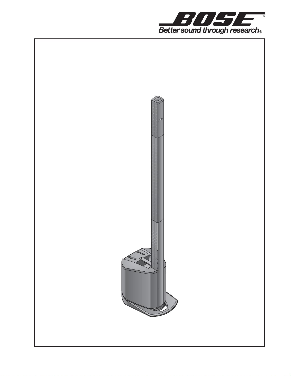
L1® Compact
Portable Line Array System
©2009 Bose Corporation
Service Manual
Reference Number 318882-SM Rev. 01
Electronic Copy Only
Page 2

Contents
Safety Information.............................................................................................................................3
Warranty .............................................................................................................................................3
Specifications....................................................................................................................................4
Electrostatic Discharge Sensitive (ESDS) Device Handling....................................................... 5
Part List Notes ..................................................................................................................................5
L1 Compact Accessory Pack...........................................................................................................5
Product Description ..................................................................................................................... 6-8
Packaging Part List, L1 Compact Power Stand (includes Array) (see Figure 1) ........................9
Figure 1. L1 Compact Power Stand Packaging View ..........................................................................9
Packaging Part List, L1 Compact Array Extensions (see Figure 2) ..........................................10
Figure 2. L1 Compact Array Extensions Packaging View .................................................................10
Main Part List, L1 Compact Power Stand (see Figure 3).......................................................11-12
Figure 3. L1 Compact Power Stand Exploded View .......................................................................... 12
Main Part List, L1 Compact Array Speaker (see Figure 4)..........................................................13
Figure 4. L1 Compact Array Speaker Exploded View ........................................................................ 13
Main Part List, L1 Compact Array Extension Exploded View (see Figure 5) ............................14
Figure 5. L1 Compact Array Extension Exploded View ..................................................................... 14
Electrical Part List .................................................................................................................... 15-37
Input/Output PCB Assembly .................................................................................................... 15-29
3.5mm Line Input PCB Assembly ...................................................................................................29
Output PCB Assembly .............................................................................................................. 29-30
Power Amplifier PCB Assembly ............................................................................................... 31-37
Disassembly Procedures ......................................................................................................... 38-44
Test Procedures ....................................................................................................................... 45-48
IC Diagrams ............................................................................................................................... 49-50
Service Manual Revision History .................................................................................................51
2
Page 3
Safety Information
1. Parts that have special safety characteristics are identified by the symbol on schematics
or by special notes on the parts list. Use only replacement parts that have critical characteristics
recommended by the manufacturer.
2. Make leakage current or resistance measurements to determine that exposed parts are
acceptably insulated from the supply circuit before returning the unit to the customer.
Use the following checks to perform these measurements:
A. Leakage Current Hot Check-With the unit completely reassembled, plug the AC line cord
directly into a 120V AC outlet. (Do not use an isolation transformer during this test.) Use a
leakage current tester or a metering system that complies with American National Standards
Institute (ANSI) C101.1 "Leakage Current for Appliances" and Underwriters Laboratories (UL)
6500 / IEC 60056 paragraph 9.1.1. With the unit AC switch first in the ON position and then in
OFF position, measure from a known earth ground (metal waterpipe, conduit, etc.) to all exposed metal parts of the unit (antennas, handle bracket, metal cabinet, screwheads, metallic
overlays, control shafts, etc.), especially any exposed metal parts that offer an electrical return
path to the chassis. Any current measured must not exceed 0.5 milliamp. Reverse the unit
power cord plug in the outlet and repeat test. ANY MEASUREMENTS NOT WITHIN THE
LIMITS SPECIFIED HEREIN INDICATE A POTENTIAL SHOCK HAZARD THAT MUST BE
ELIMINATED BEFORE RETURNING THE UNIT TO THE CUSTOMER.
B. Insulation Resistance Test Cold Check-(1) Unplug the power supply and connect a jumper
wire between the two prongs of the plug. (2) Turn on the power switch of the unit. (3) Measure
the resistance with an ohmmeter between the jumpered AC plug and each exposed metallic
cabinet part on the unit. When testing 3 wire products, the resistance measured to the product
enclosure should be between 2 and infinite MOhms. Also, the resistance measured to exposed
input/output connectors should be between 4 and infinite MOhms. When testing 2 wire products, the resistance measured to exposed input/output connectors should be between 4 and
infinite MOhms. If it is not within the limits specified, there is the possibility of a shock hazard,
and the unit must be repaired and rechecked before it is returned to the customer.
CAUTION: The Bose® L1® Compact system contains
no user-serviceable parts. To prevent warranty infractions,
refer servicing to warranty service stations or factory service.
PROPRIETARY INFORMATION
THIS DOCUMENT CONTAINS PROPRIETARY INFORMATION OF
BOSE CORPORATION WHICH IS BEING FURNISHED ONLY FOR
THE PURPOSE OF SERVICING THE IDENTIFIED BOSE PRODUCT
BY AN AUTHORIZED BOSE SERVICE CENTER OR OWNER OF
THE BOSE PRODUCT, AND SHALL NOT BE REPRODUCED OR
USED FOR ANY OTHER PURPOSE.
W arranty
The Bose L1 Compact Power Stand is covered by a limited 2-year transferable warranty.
The L1 Compact Array and the Power Stand woofer are covered by a 5-year limited warranty.
3
Page 4

Specifications
Mechanical
Part Dimensions Weight
L1 Compact Power Stand with 16.5” H x 13.25” W x 16.75” D 24.6 lbs (11.2 kg)
Loudpseaker Array (41.8 cm x 33.9 cm x 42.6 cm)
L1 Compact Loudpseaker Array 16” H x 2.75” W x 2.75” D 3.0 lbs (1.35 kg)
(40.8 cm x 7 cm x 7.1 cm)
L1 Compact Extensions (2) 32.5” H x 2.75” W x 2.75” D 2.3 lbs (1.05 kg) each
Collapsed Position 16.5” H x 13.25” W x 16.75” D 24.6 lbs (11.2 kg)
(assembled) (41.8 cm x 33.9 cm x 42.6 cm)
Extended Position 78.5” H x 13.25” W x 16.75” D 29.2 lbs (13.3 kg)
(assembled) (199.5 cm x 33.9 cm x 42.6 cm)
Shipping Cartons Weight
L1 Compact System (no extensions) 30.4 lbs (13.8 kg)
L1 Compact Extensions 7.5 lbs (3.4 kg)
Electrical
AC Power Rating
100 - 240 VAC ~ 50/60 Hz, 200W max
Peak Inrush Current
230V: 18.2 Amps
120V: 9.7 Amps
4
Page 5
Electrostatic Discharge Sensitive (ESDS)
Description Bose®
Vendor Part
Description Bose® Part Number
Device Handling
This unit contains ESDS devices. We recommend the following precautions when repairing,
replacing or transporting ESDS devices:
• Perform work at an electrically grounded work station.
• Wear wrist straps that connect to the station or heel straps that connect to conductive
floor mats.
• Avoid touching the leads or contacts of ESDS devices or PC boards even if properly
grounded. Handle boards by the edges only.
• Transport or store ESDS devices in ESD protective bags, bins, or totes. Do not insert
unprotected devices into materials such as plastic, polystyrene foam, clear plastic bags,
bubble wrap or plastic trays.
Part List Notes
1. This part is not normally available from Customer Service. Approval from the Field Service
Manager is required before ordering.
2. The individual parts located on the PCBs are listed in the Electrical Part List.
3. This part is critical for safety purposes. Failure to use a substitute replacement with the
same safety characteristics as the recommended replacement part might create shock, fire
and/or other hazards.
4. This part is referenced for informational purposes only. It is not stocked as a repair part. Refer
to the next higher assembly for a replacement part.
L1 Compact Accessory Pack
Part Number
L1 Microphone Accessory Pack,
Includes all items below
Audix OM3 Cardioid Dynamic Vocal Microphone 318884-0000 OM3
20' XLR Microphone Cable 318885-0000 CBL-20
Carton, L1 Microphone Accessory Pack, RSC,
10.50x8.50x5.75"
Cable, Audio, Dual, RCA 185931-01 N/A
Cable, Input, 3.5mm, 6ft, Black 271994-001 N/A
322711-0000 -
318886-0000 N/A
Number
L1 Compact System Versions
L1 Compact Power Stand, 120V (US) 318882-1100
L1 Compact Power Stand, 220V (China) 318882-2100
L1 Compact Power Stand, 100V (Japan) 318882-3100
L1 Compact Power Stand, 230V (Euro) 318882-4100
L1 Compact Power Stand, 240V (UK) 318882-5100
5
Page 6
Product Description
Loudspeaker
Array
Whether you are a musician amplifying your instruments, a mobile DJ entertaining an audience,
or the host of your own special event, the Bose® L1® Compact Portable Line Array System will
provide quality sound for audiences of approximately 100 people.
Features Include
• Carry it in one trip – The entire system is light enough to be carried in a single trip.
• Set it up in one minute – The interlocking components of the L1 Compact system allow system
setup in less than a minute. There are no external speaker wires required. An integrated bass
enclosure with an intuitive user interface eliminates the need for separate components.
• Fill the room with one loudspeaker – Whether you’re performing live or playing back prerecorded music, whether you’re performing in a coffeehouse or a 100-seat room, Bose Spatial
Dispersion™ loudspeaker technology provides nearly 180º of tonally balanced sound coverage
so there are no dead spots.
• PA and monitor combined – Audience members enjoy a more consistent and intimate listening
experience because the system sets up behind the performer and serves as both the monitor for
the stage and amplification system for the audience. The performer alone controls the sound.
• Versatility – In addition to musical performances, the L1 Compact provides quality sound for a
wide variety of general-purpose uses including presentations, celebrations, speeches, and
music playback for about 100 people.
• Integrated ToneMatch® signal processing – Provides a high level of tone customization on your
microphone or acoustic guitar to provide a listening experience that most musicians only achieve
using a recording studio.
• Two setup options – The L1 Compact system can be used in either the collapsed position for
smaller audiences or extended positions for larger audiences.
The L1 Compact Portable Line Array
System is shipped in two cartons.
The L1 Compact system consists of:
• L1 Compact Power Stand
• L1 Compact Loudspeaker Array
• L1 Compact Extensions
The L1 Compact system comes with
a slipcover for the Power Stand and
a padded carry bag for the L1 Compact Extensions.
Power stand carton Extensions carton
L1®Compact Power Stand
with Loudspeaker Array
AC power cord
Power Stand slipcover
L1®Compact Extensions
Extensions carry bag
6
Page 7
Product Description
Smaller audiences
• Intimate acoustic performances
• Music playback
• Presentations
• Speeches
Larger audiences
•Musical pe
rformances
–
auditorium/coeehouse
• DJ events
• Announcements
–
larger spaces
Collapsed position
Loudspeaker
Power
Extended position
Power Stand
Array
Extension
Extension
Stand
Ta b l e t o p
Array
Loudspeaker
2
3
System configurations
You can set up the L1
®
Compact system in two unique positions. The examples below will help
you quickly identify the position that can
work best for you.
The L1 Compact Extensions are not required when using the L1 Compact Portable
Line Array System in the collapsed position.
They are included for situations where you
need to elevate the Loudspeaker Array to
project sound to larger audiences.
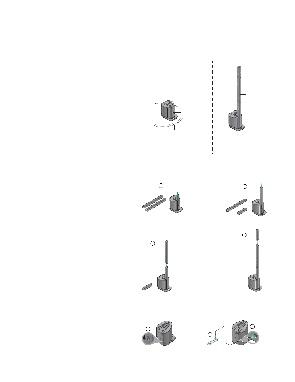
Extending the Loudspeaker Array
Once you have set the system in place:
1.Slide the Loudspeaker Array up and
out of the Power Stand and temporarily lay it aside.
Note: The two L1 Compact Extensions are identical to each other.
1
2
2.Align the plug on the bottom of the
Extension with the socket on the
Power Stand, then slide the extension
into the power stand.
3.Align the remaining Extension and
push it firmly in place.
4.Align the Loudspeaker Array and
push it firmly in place.
Connecting power to the system
1.Make sure the power switch is off
(down position).
2.Plug one end of the power cord into
the connector on the power stand.
3.Plug the other end into a live electrical receptacle.
4.Before turning the system on,
connect your sound sources.
4
3
1
7
Page 8
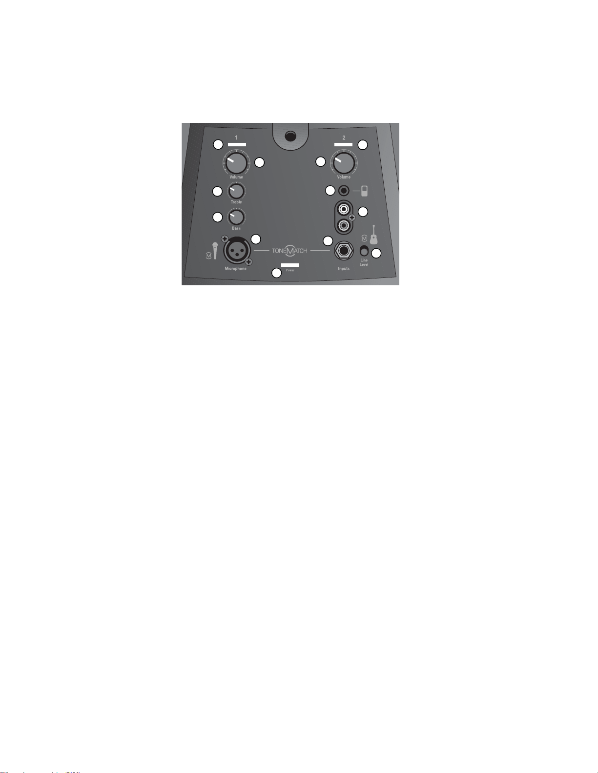
Product Description
Channel 1
Channel 2
1
2
3
4
5
6
7
8
9
10
11
12
Connections and controls
The power stand control panel provides all the necessary connectors, controls, and indicators
for operation.
(Microphone input)
The channel 1 input is for use only with a
microphone. Integrated ToneMatch
®
signal
processing provides a high level of tone
customization to provide a listening experience
that most musicians can only achieve using a
recording studio.
1. S igna l/Clip indic ator – Displays the input
signal status in color.
• Green: Input signal present
• Red: Input signal clipping
2. V olume contr ol – Adjusts the volume of your
microphone.
3. Treble control – Adjusts the amount of treble
on your microphone.
4. B ass c ontr ol – Adjusts the amount bass on
your microphone.
5. Microphone input – Analog input for
connecting a balanced XLR microphone cable. A
ToneMatch microphone preset is built in.
(Utilit y cha nne l – multip le input)
6. S igna l/Clip indicator – Displays the input
signal status in color.
• Green: Input signal present
• Red: Input signal clipping
7.V olume contr ol – Adjusts the overall volume of
all input sources connected to Channel 2.
8. 1/8-inch stereo input – Stereo analog input
for connecting audio sources such as portable
mp3 players, satellite radio, laptop computers,
video projectors, and smart boards. Left and right
inputs are summed by the power stand.
9. RCA stereo input – Analog input for
connecting audio sources such as DVD players,
VCR players, video game consoles, DJ mixers,
Keyboards and other instruments. For best
results, connect both the left and right signals.
Left and right inputs are summed by the power
stand.
10. 1/4-inch input – Balanced analog input for
connecting guitars and other instruments.
Accepts either 1/4-inch TRS balanced or TS
unbalanced cables.
11. ToneMatch switch – When connecting an
acoustic guitar to the 1/4-inch input, move the
switch to the position to enable a ToneMatch
preset. When connecting anything other than an
acoustic guitar to the 1/4-inch input, move the
switch down to the Line Level position.
12. Power LED – Indicates power status.
Blue: Power on
8
Page 9
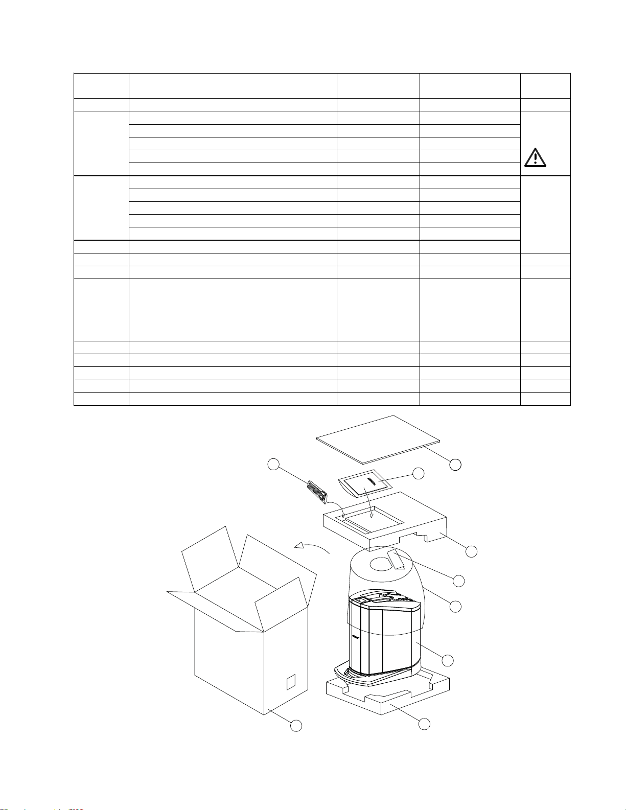
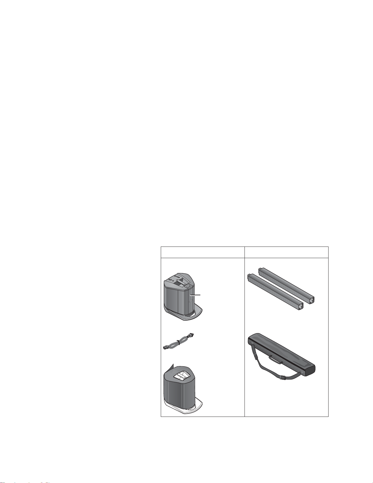
Packaging Part List
L1 Compact Power Stand (includes Array) (see Figure 1)
Item
Number
Description Bose® Part
Number
Vendor Part
Number
Note
1 Inner Sheet, Cardboard 324116-001S 1451-0340+0
2 Power Cord, 120V, (US) 298165 7012-7340+0 3
Power Cord, 220V (China) 318882-210S 7013-0580+0
Power Cord, 100V, (Japan) 298167 7012-5530+0
Power Cord, 230V (Euro) 298166 7012-6980+0
Power Cord, 240V (UK) 298168 7012-6603+0
3 Owner’s Guide, 3 Lang (US/UK) 317638-0010 4301-7353+0
Owner’s Guide (Euro) 320042-0010 4301-7354+0
Owner’s Guide (China) 320043-0010 4301-7356+0
Owner’s Guide (Japan) 320044-0010 4301-7352+0
2YR Warranty Card, Registration 320561-0010 3050-4571+0
4 Filler, Top, Power Stand 317383-000S 1493-2001+0
5 Quick Start Guide Card 317639-0010 3050-4561+0
6 Power Stand Slip Cover 317403-010S 4201-1180+0
7 L1 Compact Power Stand, 120V (US) REF -
L1 Compact Power Stand, 220V (China) REF -
L1 Compact Power Stand, 100V (Japan) REF -
L1 Compact Power Stand, 230V (Euro) REF -
L1 Compact Power Stand, 240V (UK) REF -
8 Filler, Bottom, Power Stand 317384-000S 1493-2011+0
9 Carton, Powerstand 317382-000S 1481-4801+0
- L1 Compact Loudspeaker Array 318880-0100 svc-cajun11+arra
- Warranty Card, English Language 307430 3050-3531+0
- Poly Bag 320228-0000 1497-4122+0
2
9
3
7
8
Figure 1. L1 Compact Power Stand Packaging View
1
4
5
6
9
Page 10
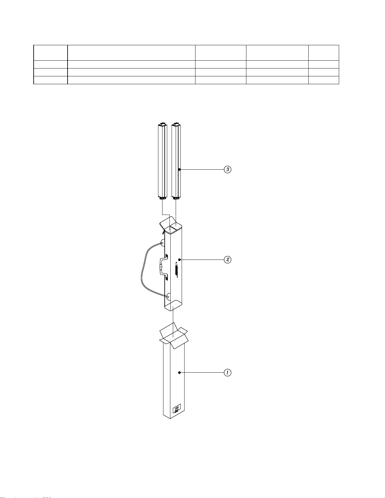
Packaging Part List
Item
Description Bose® Part
Vendor Part
Note
L1 Compact Array Extensions (see Figure 2)
Number
1 Carton, Extensions 317385-000S 1481-4701+0
2 Extensions Carry Bag 317404-010S 4201-1170+0
3 L1 Compact Extension 318881-010S svc-cajun11+exte
Number
Number
Figure 2. L1 Compact Array Extensions Packaging View
10
Page 11
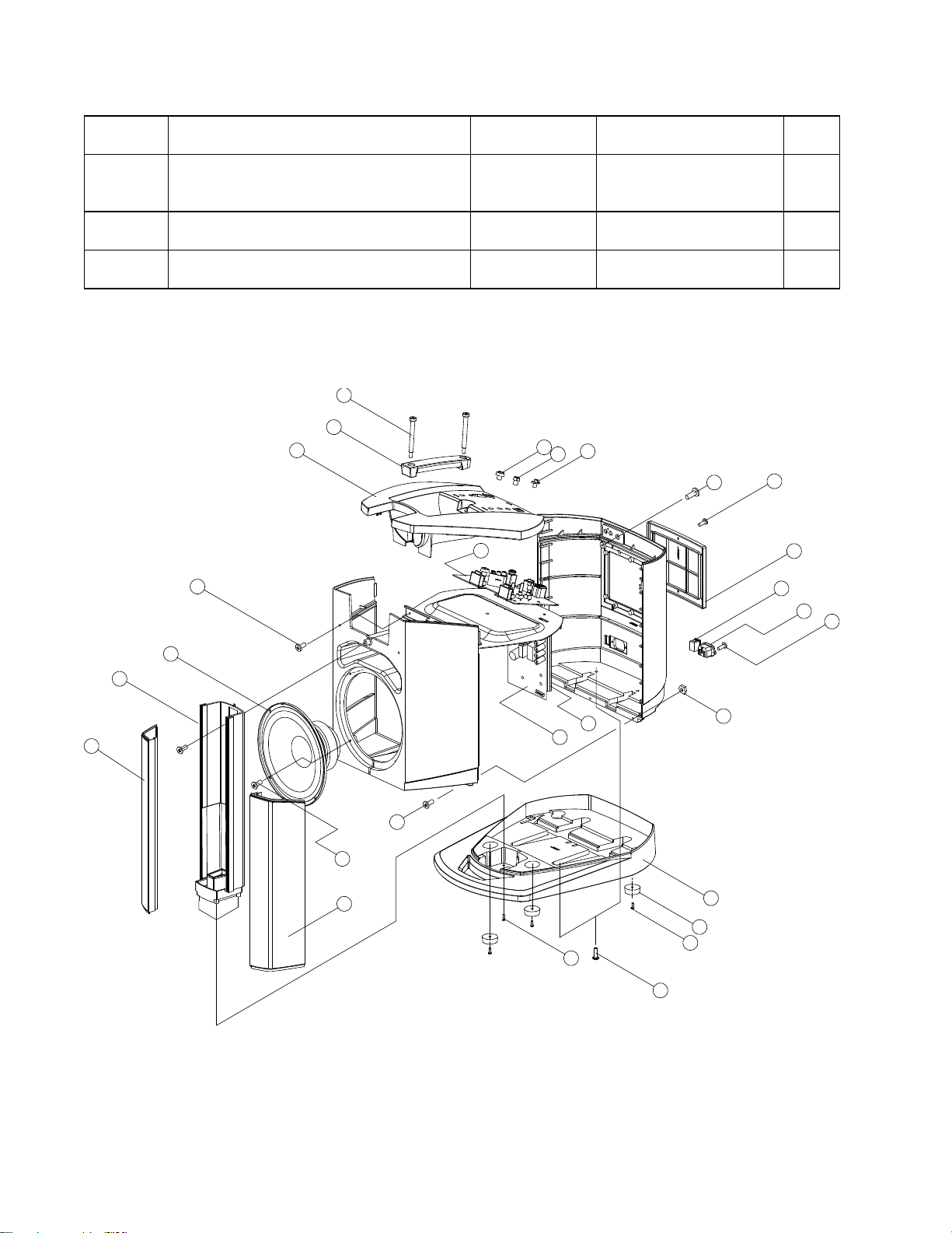
Main Part List
Item
Description Bose® Part
Vendor Part Number Note
L1 Compact Power Stand (see Figure 3)
Number
1 Grille, Power Stand, Left 317363-010S 4135+8921+0
2 Grille, Power Stand, Right 317364-010S 4135-8931+0
3 Guide, Array, ABS, Blk - 4155-3811+0
4 Woofer, 8 inch 317370-000S SVC-8900-6980+0
5 Screw, M4x25mm - 2900-4025+3000 4
6 Screw, M4x14 - 2904-4014+3000 4
7 Enclosure, Top, Silk Screened 317346-010S 1468-5501+0
8 Carry Handle, Power Stand 317353-010S 4155-3781+0
9 Bolt, Power Stand Carry Handle, M6 317359-010S 4135-8951+0
10 PCB Assy, IO COM
(Pre-amp PCB ASSY)
11 Knob, Channel 1/2 317349-010S 2447-8401+0
12 Knob, Volume/Treble 317350-010S 2447-8501+0
13 Knob, Line Level 317351-010S 2447-8601+0
14 Screw, Machine, Flat, CS, M4x12 - 2901-4012+3000 4
15 Screw, CSH, Blk - 2901-3012+3000 4
16 Panel, Access 317348-010S 1468-5701+0
17 Switch, Power, DPST, 250V, 10A 317373-000S 5200-4969+0 3
18 Inlet, AC, UL/CSA/VDE, 250V - 2113-1144+0 3
19 Screw, M3x12, CSH, Blk - 2901-3012+3000 4
20 Nut, M4 - 2640-4030+0703 4
21 Heatsink, Amplifier PCB, 160x120mm - 5401-0191+0 4
22 PCB Assy, Amp/SMPS 317372-000S SVC-CAJUN01+PAMP 2
23 Screw, Machine, M4 - 2904-4020+3000 4
24 Enclosure, Bottom 317347-010S 1468-5601+0
25 Foot, Rubber, 31x31x10 - 4157-1191+0 3
26 Screw, B-tite, Bind, M4x12 - 2954-4012+3000 4
27 Screw, Machine, M4x25, 7.8mm - 2900-4025+3000 4
28 Screw, B-tite, Flat-CS, M3x12 - 2951-3012+0000 4
- Guide Track, Bass 317358-010S 4155-3841+0
- FUSE, 5A, 250V, 8X8.5,
VDE/PSE/CCC, RLT LITTELFUSE,
JAPAN/EURO/UK
- FUSE, 5A, 250V, 8X8.5 UL/CSA
RLT LITTELFUSE, US/CAN
- Ribbon Cable, I/O Board to
AMP/SMPS, WIRE-CONN, 10P, P2.0,
#26, UL2468 F/F
- Cable Assy, AMP/SMPS to Woofer,
WIRE-SPK, 2P, VH3.96-2Y, #20,
UL2468, L400, R/B, 205/110T
- Cable Assy, AMP/SMPS to Twiddler
Conn., WIRE, 2P, VH3.96-3Y, #20, UL
2468, L=500, R/B, WM17700ND
Number
319966-000S SVC-CAJUN01+I/O 2
317381-000S 5120-1136+0-L 3
319970-000S 5120-1140+0-L 3
319983-000S 7013-0590+0 3
319984-000S 7013-0780+0 3
319985-000S 7013-0730+0 3
11
Page 12
Main Part List
Item
Description Bose® Part
Vendor Part Number Note
L1 Compact Power Stand, continued (see Figure 3)
Number
- PCB Assy, COB COM
(Includes: PRE-AMP ASSY/3.5MM
Jack Input Card/Line Output Card)
- PCB Assy, IN COM
(3.5MM Jack Input Card)
- PCB Assy, OUT COM
(Line Output Card)
6
Number
317371-000S SVC-CAJUN01+COB 2
319967-000S SVC-CAJUN01+IN 2
319968-000S SVC-CAJUN01+OUT 2
9
8
7
10
11
13
12
14
15
17
16
18
19
4
3
21
1
23
5
2
22
28
27
20
24
25
26
Figure 3. L1 Compact Power Stand Exploded View
12
Page 13
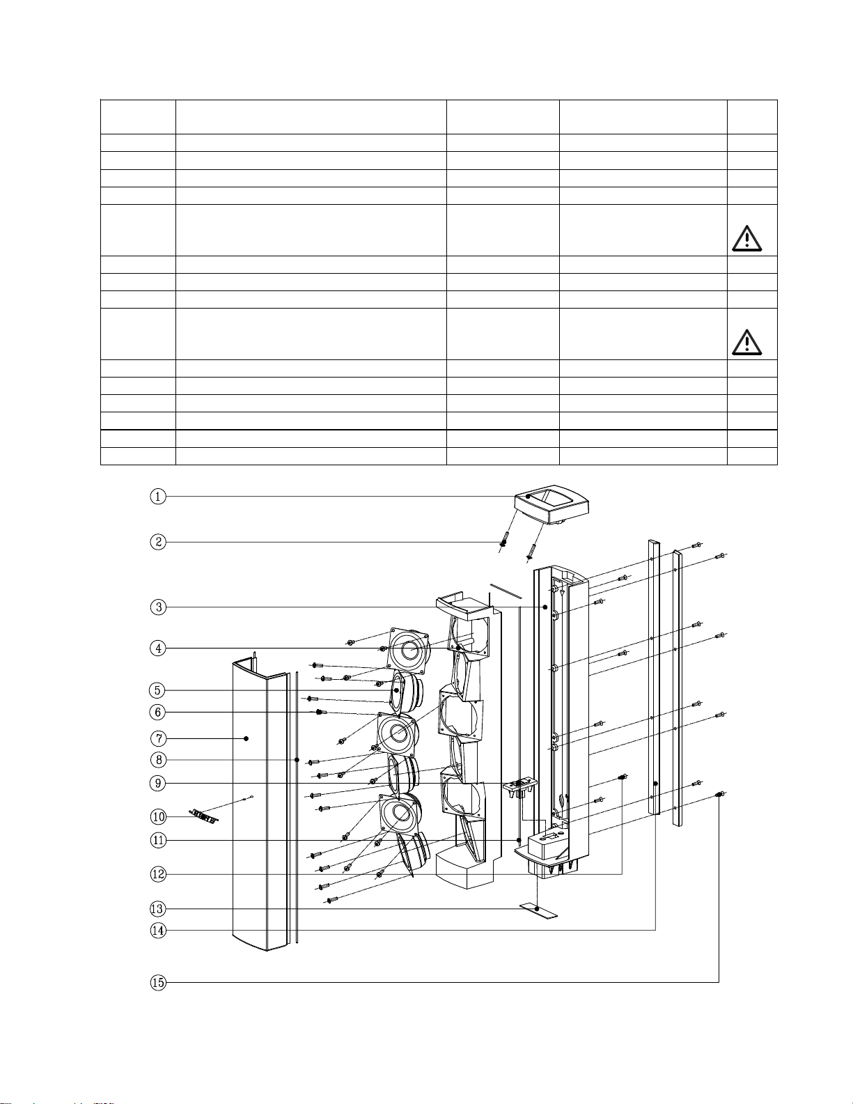
Main Part List
Item
Description Bose® Part
Vendor Part Number Note
L1 Compact Array Speaker (see Figure 4)
Number
1 Handle, Array - 4155-3851+0 4
2 Screw, B-tite, Bind, M3x16, CS-Recess - 2954-3016+3000 4
3 Enclosure, Array, ABS - 4155-3801+0 4
4 Baffle, Array, ABS, Black - 4155-3791+0 4
5 Twiddler, 2.5 inch 291636-001 1525-2120+0 3
6 Screw, M3x10, BT, ZN, Blk - 2934-3010+3000 4
7 Grille, Array (W/Logo) 317365-010S svc-cajun01+gril
8 Butyl Tape - 9500-1101+0 4
9 Wire, Spk, 2P, #20, UL1007,
L=250/180, RD/BLK
10 Array Logo 317407-010S 2150-7311+0
11 EVA Gasket, Baffle - 4149-1121+0 4
12 Screw, M3x13, 5.6MM, BK-ZN/CR HD - 2931-3013+3000 4
13 Label, Serial Number, 30x7mm - - 4
14 Guide Strip, Array 317366-010S 4155-3861+0
15 Screw, M3x12, CSH, BK - 2901-3012+3000 4
Number
- 7013-0760+0 3, 4
Figure 4. L1 Compact Array Speaker Exploded View
13
Page 14
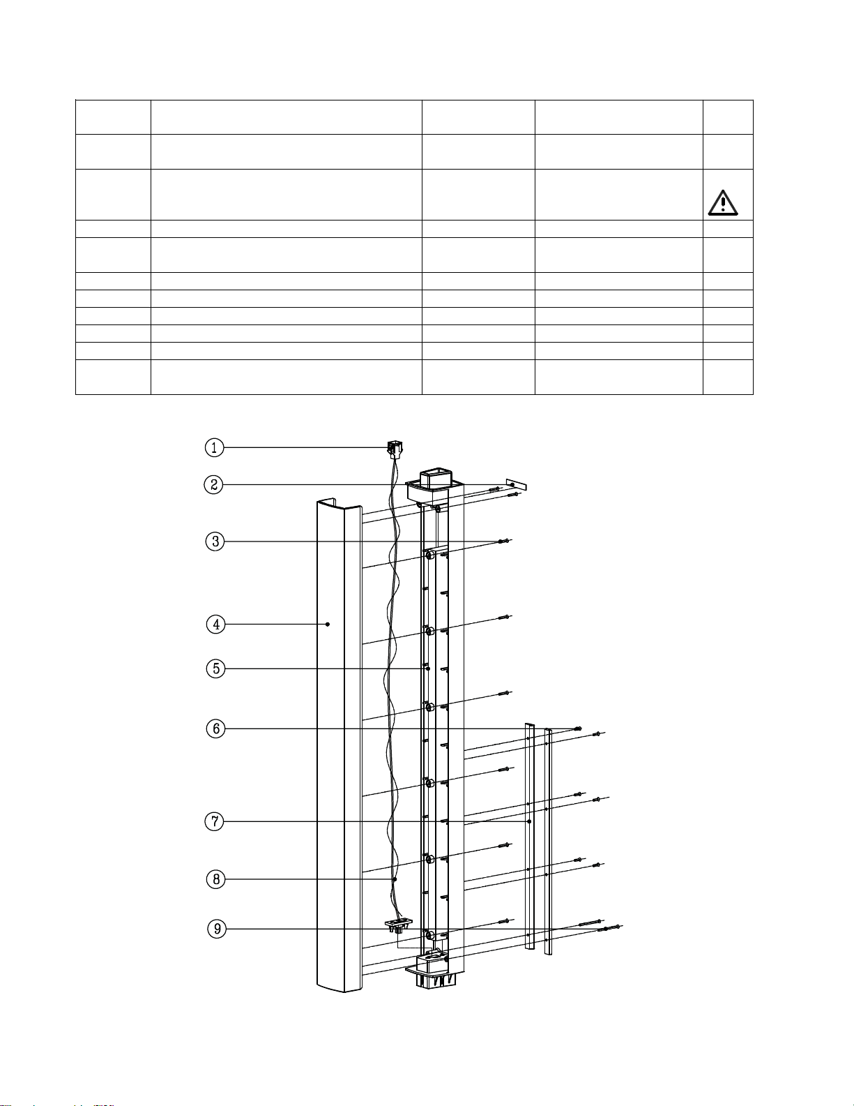
Main Part List
Item
Description Bose® Part
Vendor Part Number Note
L1 Compact Array Extension Exploded View (see Figure 5)
Number
- Array Extension, Complete Assembly,
Consists of below items
1 Wire, 2P, #20, UL2468, L=850
Red/Blk, Molex MDI
2 Label, Serial Number, 30x7mm - - 4
3 Screw, B-tite, Flat-CS, M3x16, CS-
Recess, BZ
4 Extension Front, ABS, Blk - 4155-3821+0 4
5 Extension Rear, ABS, Blk - 4155-3831+0 4
6 MS Screw, M3x12, CSH, BK - 2901-3012+3000 4
7 Guide Strip, POM, Blk - 4155-3861+0 4
8 Gasket - 4153-3431+0 4
9 Screw, Machine, Flat-CS, M3x40, CS-
Recess, BZ
Note: The array extensions are not repairable. The above parts are listed for reference only.
Number
318881-010S svc-cajun11+exte
- 7013-0750+0 3, 4
- 2951-3016+3000 4
- 2901-3040+3000 4
Figure 5. L1 Compact Array Extension Exploded View
14
Page 15

Reference
Description Vendor Part Number Note
Electrical Part List
Input/Output PCB Assembly
Resistors
Designator
R100 100 OHM, RMG, 1/16W, 1%, 0603 4723-101A+P 4
R101 100 OHM, RMG, 1/16W, 1%, 0603 4723-101A+P 4
R102 2K, RMG, 1/16W, 1%, 0603/1608 4723-202A+P 4
R103 2K, RMG, 1/16W, 1%, 0603/1608 4723-202A+P 4
R104 4.99K, RMG, 1/16W, 1%, 0603 4723-4991+P 4
R105 4.99K, RMG, 1/16W, 1%, 0603 4723-4991+P 4
R106 4.99K, RMG, 1/16W, 1%, 0603 4723-4991+P 4
R107 4.99K, RMG, 1/16W, 1%, 0603 4723-4991+P 4
R108 10K, RMG, 1/16W, 1%, 0603/1608 4723-103A+P 4
R109 10K, RMG, 1/16W, 1%, 0603/1608 4723-103A+P 4
R110 1K, RMG, 1/16W, 1%, 0603/1608 4723-102A+P 4
R111 1K, RMG, 1/16W, 1%, 0603/1608 4723-102A+P 4
R112 0 OHM, RMG, 1/16W, 5%, 0603 4723-000J+P-R 4
R113 1K, RMG, 1/16W, 1%, 0603/1608 4723-102A+P 4
R114 150 OHM, RMG, 1/16W, 1%, 0603 4723-151A+P-R 4
R115 150 OHM, RMG, 1/16W, 1%, 0603 4723-151A+P-R 4
R116 2.2K, RMG, 1/16W, 1%, 0603/1608 4723-222A+P 4
R117 150 OHM, RMG, 1/16W, 1%, 0603 4723-151A+P 4
R118 1M, RMG, 1/16W, 1%, 0603 4723-105A+P 4
R119 1M, RMG, 1/16W, 1%, 0603 4723-105A+P 4
R120 100K, RMG, 1/16W, 1%, 0603 4723-104A+P 4
R122 39K, RMG, 1/10W, 1%, 0603 4720-393A+P 4
R123 39K, RMG, 1/10W, 1%, 0603 4720-393A+P 4
R124 12K, RMG, 1/16W, 1%, 0603 4723-123A+P 4
R125 150 OHM, RMG, 1/16W, 1%, 0603 4723-154A+P-R 4
R126 75K, RMG, 1/16W, 1%, 0603 4723-753A+P 4
R127 8.87K, RMG, 1/16W, 1%, 0603/1608 4723-8871+P 4
R128 47K, RMG, 1/16W, 1%, 0603/1608 4723-473A+P 4
R129 60.4K, RMG, 1/16W, 1%, 0603/1608 4723-6042+P 4
R130 1K, RMG, 1/16W, 1%, 0603/1608 4723-102A+P 4
R131 10K, RMG, 1/16W, 1%, 0603/1608 4723-103A+P 4
R132 10K, RMG, 1/16W, 1%, 0603/1608 4723-103A+P 4
R133 100K, RMG, 1/16W, 1%, 0603 4723-104A+P-R 4
R134 100K, RMG, 1/16W, 1%, 0603 4723-104A+P-R 4
R135 97.6K, RMG, 1/10W, 1%, 0603 4720-9762+P 4
R136 100K, RMG, 1/16W, 1%, 0603 4723-104A+P-R 4
R137 0 OHM, RMG, 1/16W, 5%, 0603 4723-000J+P-R 4
R138 0 OHM, RMG, 1/16W, 5%, 0603 4723-000J+P-R 4
R139 100K, RMG, 1/16W, 1%, 0603 4723-104A+P-R 4
R140 100K, RMG, 1/16W, 1%, 0603 4723-104A+P-R 4
R141 10K, RMG, 1/16W, 1%, 0603 4723-103A+P-R 4
R142 43.2K, RMG, 1/10W, 1%, 0603 4720-4322+P 4
R143 100K, RMG, 1/16W, 1%, 0603 4723-104A+P-R 4
R144 100K, RMG, 1/16W, 1%, 0603 4723-104A+P-R 4
R145 100K, RMG, 1/16W, 1%, 0603 4723-104A+P-R 4
R146 100K, RMG, 1/16W, 1%, 0603 4723-104A+P-R 4
R147 10K, RMG, 1/16W, 1%, 0603 4723-103A+P-R 4
15
Page 16

Reference
Description Vendor Part Number Note
Electrical Part List
Input/Output PCB Assembly
Resistors (continued)
Designator
R148 10K, RMG, 1/16W, 1%, 0603 4723-103A+P-R 4
R149 270 OHM, RMG, 1/16W, 1%, 0603 4723-271A+P-R 4
R150 270 OHM, RMG, 1/16W, 1%, 0603 4723-271A+P-R 4
R151 34.8K, RMG, 1/10W, 1%, 0603 4720-3482+P 4
R152 68K, RMG, 1/16W, 1%, 0603 4723-683A+P-R 4
R153 10K, RMG, 1/16W, 1%, 0603 4723-103A+P-R 4
R154 48.7K, RMG, 1/10W, 1%, 0603 4720-4872+P 4
R155 17.8K, RMG, 1/16W, 1%, 0603/1608 4723-1782+P 4
R156 20K, RMG, 1/16W, 1%, 0603/1608 4723-203A+P 4
R157 10K, RMG, 1/16W, 1%, 0603 4723-103A+P-R 4
R158 6.81K, RMG, 1/10W, 1%, 0603 4720-6811+P 4
R159 13.7K, RMG, 1/10W, 1%, 0603 4720-1372+P 4
R160 10K, RMG, 1/16W, 1%, 0603 4723-103A+P-R 4
R161 10K, RMG, 1/16W, 1%, 0603 4723-103A+P-R 4
R162 1K, RMG, 1/16W, 1%, 0603/1608 4723-102A+P 4
R163 24K, RMG, 1/16W, 1%, 0603 4723-243A+P 4
R164 24K, RMG, 1/16W, 1%, 0603 4723-243A+P 4
R165 100K, RMG, 1/16W, 1%, 0603 4723-104A+P-R 4
R166 22K, RMG, 1/16W, 1%, 0603 4723-223A+P-R 4
R167 8.87K, RMG, 1/16W, 1%, 0603/1608 4723-8872+P 4
R168 12K, RMG, 1/16W, 1%, 0603 4723-123A+P 4
R169 3K, RMG, 1/16W, 1%, 0603 4723-302A+P 4
R170 24K, RMG, 1/16W, 1%, 0603 4723-243A+P 4
R172 820 OHM, RMG, 1/16W, 1%, 0603/1608 4723-821A+P 4
R173 820 OHM, RMG, 1/16W, 1%, 0603/1608 4723-821A+P 4
R174 0 OHM, RMG, 1/16W, 5%, 0603 4723-000J+P-R 4
R175 0 OHM, RMG, 1/16W, 5%, 0603 4723-000J+P 4
R177 510 OHM, RMG, 1/4W, 5%, 1206 4725-511J+6 4
R178 510 OHM, RMG, 1/4W, 5%, 1206 4725-511J+6 4
R179 100K, RMG, 1/16W, 1%, 0603 4723-104A+P-R 4
R180 15.8K, RMG, 1/10W, 1%, 0603 4720-1582+P 4
R181 470K, RMG, 1/16W, 1%, 0603 4723-474A+P 4
R182 0 OHM, RMG, 1/16W, 5%, 0603 4723-000J+P-R 4
R183 24K, RMG, 1/16W, 1%, 0603 4723-243A+P 4
R184 100K, RMG, 1/16W, 1%, 0603 4723-104A+P-R 4
R186 1M, RMG, 1/16W, 1%, 0603 4723-105A+P 4
R188 10 OHM, RMG, 1/16W, 1%, 0603 4723-100A+P-R 4
R189 10 OHM, RMG, 1/16W, 1%, 0603 4723-100A+P-R 4
R190 1M, RMG, 1/16W, 1%, 0603 4723-105A+P 4
R199 100 OHM, RMG, 1/16W, 1%, 0603 4723-101A+P 4
R200 45.3K, RMG, 1/10W, 1%, 0603 4720-4532+P 4
R201 95.3K, RMG, 1/10W, 1%, 0603 4720-9532+P 4
R202 59K, RMG, 1/10W, 1%, 0603 4720-593A+P 4
R203 12K, RMG, 1/16W, 1%, 0603 4723-123A+P 4
R204 7.87K, RMG, 1/10W, 1%, 0603 4720-7871+P 4
R205 9.76K, RMG, 1/16W, 1%, 0603 4723-9761+P 4
R206 9.76K, RMG, 1/16W, 1%, 0603 4723-9761+P 4
R207 95.3K, RMG, 1/10W, 1%, 0603 4720-9532+P 4
R208 7.87K, RMG, 1/10W, 1%, 0603 4720-7871+P 4
16
Page 17

Reference
Description Vendor Part Number Note
Electrical Part List
Input/Output PCB Assembly
Resistors (continued)
Designator
R209 12K, RMG, 1/16W, 1%, 0603 4723-123A+P 4
R210 150 OHM, RMG, 1/16W, 1%, 0603 4723-154A+P-R 4
R211 75K, RMG, 1/16W, 1%, 0603 4723-753A+P 4
R213 1K, RMG, 1/16W, 1%, 0603/1608 4723-102A+P 4
R214 1K, RMG, 1/16W, 1%, 0603/1608 4723-102A+P 4
R215 100 OHM, RMG, 1/16W, 1%, 0603 4723-101A+P 4
R216 10K, RMG, 1/16W, 1%, 0603/1608 4723-103A+P 4
R217 1K, RMG, 1/16W, 1%, 0603/1608 4723-102A+P 4
R218 20K, RMG, 1/16W, 1%, 0603/1608 4723-203A+P 4
R219 2K, RMG, 1/16W, 1%, 0603/1608 4723-202A+P 4
R220 4.99K, RMG, 1/16W, 1%, 0603 4723-4991+P 4
R222 68K, RMG, 1/16W, 1%, 0603 4723-683A+P-R 4
R223 100K, RMG, 1/16W, 1%, 0603 4723-104A+P 4
R224 10K, RMG, 1/16W, 1%, 0603/1608 4723-103A+P 4
R225 1.8M, RMG, 1/16W, 1%, 0603 4723-185A+P 4
R226 10K, RMG, 1/16W, 1%, 0603/1608 4723-103A+P 4
R227 1.8M, RMG, 1/16W, 1%, 0603 4723-185A+P 4
R228 100 OHM, RMG, 1/16W, 1%, 0603 4723-101A+P 4
R229 100 OHM, RMG, 1/16W, 1%, 0603 4723-101A+P 4
R230 1K, RMG, 1/16W, 1%, 0603/1608 4723-102A+P 4
R231 0 OHM, RMG, 1/16W, 5%, 0603 4723-000J+P 4
R232 1M, RMG, 1/16W, 1%, 0603 4723-105A+P 4
R234 0 OHM, RMG, 1/16W, 5%, 0603 4723-000J+P-R 4
R236 3.9K, RMG, 1/16W, 1%, 0603/1608 4723-392A+P 4
R238 2K, RMG, 1/16W, 1%, 0603/1608 4723-202A+P 4
R239 2K, RMG, 1/16W, 1%, 0603/1608 4723-202A+P 4
R240 3.9K, RMG, 1/16W, 1%, 0603/1608 4723-392A+P 4
R241 3.9K, RMG, 1/16W, 1%, 0603/1608 4723-392A+P 4
R243 0 OHM, RMG, 1/16W, 5%, 0603 4723-000J+P-R 4
R244 10K, RMG, 1/16W, 1%, 0603 4723-103A+P-R 4
R245 10K, RMG, 1/16W, 1%, 0603 4723-103A+P-R 4
R246 1.8M, RMG, 1/16W, 1%, 0603 4723-185A+P 4
R247 59K, RMG, 1/10W, 1%, 0603 4720-593A+P 4
R248 1M, RMG, 1/16W, 1%, 0603 4723-105A+P 4
R249 20K, RMG, 1/16W, 1%, 0603/1608 4723-203A+P 4
R250 24K, RMG, 1/16W, 1%, 0603 4723-243A+P 4
R251 1M, RMG, 1/16W, 1%, 0603 4723-105A+P 4
R254 24K, RMG, 1/16W, 1%, 0603 4723-243A+P 4
R255 68K, RMG, 1/16W, 1%, 0603 4723-683A+P-R 4
R257 68K, RMG, 1/16W, 1%, 0603 4723-683A+P-R 4
R258 10 OHM, RMG, 1/16W, 1%, 0603 4723-100A+P-R 4
R260 100 OHM, RMG, 1/16W, 1%, 0603 4723-101A+P 4
R262 100K, RMG, 1/16W, 1%, 0603 4723-104A+P 4
R264 1.8M, RMG, 1/16W, 1%, 0603 4723-185A+P 4
R265 6.8K, RMG, 1/16W, 1%, 0603/1608 4723-682A+P 4
R266 6.8K, RMG, 1/16W, 1%, 0603/1608 4723-682A+P 4
R267 22.6K, RMG, 1/10W, 1%, 0603 4720-2262+P 4
R271 510 OHM, RMG, 1/4W, 5%, 1206 4725-511J+6 4
17
Page 18

Reference
Description Vendor Part Number Note
Electrical Part List
Input/Output PCB Assembly
Resistors (continued)
Designator
R272 510 OHM, RMG, 1/4W, 5%, 1206 4725-511J+6 4
R275 100K, RMG, 1/16W, 1%, 0603 4723-104A+P-R 4
R276 15.8K, RMG, 1/10W, 1%, 0603 4720-1582+P 4
R277 470K, RMG, 1/16W, 1%, 0603 4723-474A+P 4
R278 0 OHM, RMG, 1/16W, 5%, 0603 4723-000J+P-R 4
R279 24K, RMG, 1/16W, 1%, 0603 4723-243A+P 4
R280 100K, RMG, 1/16W, 1%, 0603 4723-104A+P-R 4
R282 1M, RMG, 1/16W, 1%, 0603 4723-105A+P 4
R283 68K, RMG, 1/16W, 1%, 0603 4723-683A+P-R 4
R285 2.2K, RMG, 1/16W, 1%, 0603/1608 4723-222A+P 4
R287 100K, RMG, 1/16W, 1%, 0603 4723-104A+P 4
R288 2K, RMG, 1/16W, 1%, 0603/1608 4723-202A+P 4
R289 33K, RMG, 1/16W, 1%, 0603 4723-333A+P-R 4
R290 15.8K, RMG, 1/10W, 1%, 0603 4720-1582+P 4
R300 33K, RMG, 1/16W, 1%, 0603 4723-333A+P-R 4
R301 68K, RMG, 1/16W, 1%, 0603 4723-683A+P-R 4
R302 91K, RMG, 1/10W, 1%, 0603 4720-913A+P 4
R303 68K, RMG, 1/16W, 1%, 0603 4723-683A+P-R 4
R304 10K, RMG, 1/16W, 1%, 0603 4723-103A+P-R 4
R305 100K, RMG, 1/16W, 1%, 0603 4723-104A+P-R 4
R306 10K, RMG, 1/16W, 1%, 0603 4723-103A+P-R 4
R307 20K, RMG, 1/16W, 1%, 0603/1608 4723-203A+P 4
R308 100K, RMG, 1/16W, 1%, 0603 4723-104A+P-R 4
R309 33K, RMG, 1/16W, 1%, 0603 4723-333A+P-R 4
R311 10K, RMG, 1/16W, 1%, 0603 4723-103A+P-R 4
R312 10K, RMG, 1/16W, 1%, 0603 4723-103A+P-R 4
R313 100K, RMG, 1/16W, 1%, 0603 4723-104A+P-R 4
R314 10K, RMG, 1/16W, 1%, 0603 4723-103A+P-R 4
R315 10K, RMG, 1/16W, 1%, 0603 4723-103A+P-R 4
R316 20K, RMG, 1/16W, 1%, 0603/1608 4723-203A+P 4
R317 10K, RMG, 1/16W, 1%, 0603 4723-103A+P-R 4
R318 13.7K, RMG, 1/10W, 1%, 0603 4720-1372+P 4
R319 13.7K, RMG, 1/10W, 1%, 0603 4720-1372+P 4
R320 200K, RMG, 1/16W, 1%, 0603/1608 4723-204A+P 4
R321 20K, RMG, 1/16W, 1%, 0603/1608 4723-203A+P 4
R322 20K, RMG, 1/16W, 1%, 0603/1608 4723-203A+P 4
R325 1K, RMG, 1/16W, 1%, 0603/1608 4723-102A+P 4
R326 330 OHM, RMG, 1/16W, 1%, 0603 4723-331A+P 4
R327 10 OHM, RMG, 1/16W, 1%, 0603 4723-100A+P-R 4
R328 470 OHM, RMG, 1/16W, 1%, 0603 4723-471A+P-R 4
R329 470 OHM, RMG, 1/16W, 1%, 0603 4723-471A+P-R 4
R332 20K, RMG, 1/16W, 1%, 0603/1608 4723-203A+P 4
R333 80.6K, RMG, 1/10W, 1%, 0603 4720-8062+P 4
R334 3K, RMG, 1/16W, 1%, 0603 4723-302A+P 4
R335 10K, RMG, 1/16W, 1%, 0603/1608 4723-103A+P 4
R336 24K, RMG, 1/16W, 1%, 0603 4723-243A+P 4
R337 20K, RMG, 1/16W, 1%, 0603/1608 4723-203A+P 4
R338 39K, RMG, 1/16W, 1%, 0603/1608 4723-393A+P 4
R339 10K, RMG, 1/16W, 1%, 0603 4723-103A+P-R 4
18
Page 19

Reference
Description Vendor Part Number Note
Electrical Part List
Input/Output PCB Assembly
Resistors (continued)
Designator
R340 10K, RMG, 1/16W, 1%, 0603 4723-103A+P-R 4
R341 158K, RMG, 1/10W, 1%, 0603 4720-1583+P 4
R342 23.2K, RMG, 1/16W, 1%, 0603/1608 4723-2322+P 4
R343 24.3K, RMG, 1/10W, 1%, 0603 4720-2432+P 4
R344 24.3K, RMG, 1/10W, 1%, 0603 4720-2432+P 4
R345 10K, RMG, 1/16W, 1%, 0603 4723-103A+P-R 4
R346 10K, RMG, 1/16W, 1%, 0603 4723-103A+P-R 4
R347 14K, RMG, 1/16W, 1%, 0603/1608 4723-143A+P 4
R348 7.15K, RMG, 1/16W, 1%, 0603/1608 4723-7151+P 4
R349 1M, RMG, 1/16W, 1%, 0603 4723-105A+P 4
R351 80.6K, RMG, 1/10W, 1%, 0603 4720-8062+P 4
R352 20K, RMG, 1/16W, 1%, 0603/1608 4723-203A+P 4
R353 100K, RMG, 1/16W, 1%, 0603 4723-104A+P 4
R354 4.99K, RMG, 1/16W, 1%, 0603 4723-4991+P 4
R356 5.36K, RMG, 1/10W, 1%, 0603 4720-5361+P 4
R357 100K, RMG, 1/16W, 1%, 0603 4723-104A+P-R 4
R358 1.96K, RMG, 1/10W, 1%, 0603 4720-1961+P 4
R359 14K, RMG, 1/16W, 1%, 0603 4723-143A+P 4
R366 107K, RMG, 1/10W, 1%, 0603 4720-1073+P 4
R367 1K, RMG, 1/16W, 1%, 0603/1608 4723-102A+P 4
R368 53.6K, RMG, 1/10W, 1%, 0603 4720-5362+P 4
R369 100K, RMG, 1/16W, 1%, 0603 4723-104A+P-R 4
R373 8.45K, RMG, 1/10W, 1%, 0603 4720-8451+P 4
R376 23.2K, RMG, 1/16W, 1%, 0603/1608 4723-2322+P 4
R378 107K, RMG, 1/10W, 1%, 0603 4720-1073+P 4
R381 97.6K, RMG, 1/10W, 1%, 0603 4720-9762+P 4
R386 470K, RMG, 1/16W, 1%, 0603 4723-474A+P 4
R391 470K, RMG, 1/16W, 1%, 0603 4723-474A+P 4
R392 47K, RMG, 1/16W, 1%, 0603 4723-473A+P-R 4
R393 24K, RMG, 1/16W, 1%, 0603 4723-243A+P 4
R394 33K, RMG, 1/16W, 1%, 0603 4723-333A+P-R 4
R395 10K, RMG, 1/16W, 1%, 0603/1608 4723-103A+P 4
R396 33K, RMG, 1/16W, 1%, 0603 4723-333A+P-R 4
R397 47K, RMG, 1/16W, 1%, 0603 4723-473A+P-R 4
R399 0 OHM, RMG, 1/16W, 5%, 0603 4723-000J+P 4
R400 33K, RMG, 1/16W, 1%, 0603 4723-333A+P-R 4
R401 47 OHM, RMG, 1/2W, 1%, 2010 4727-470A+W 4
R402 20K, RMG, 1/16W, 1%, 0603/1608 4723-203A+P 4
R403 4.7M, RMG, 1/10W, 1%, 0603 4720-475A+P 4
R404 20K, RMG, 1/16W, 1%, 0603/1608 4723-203A+P 4
R405 20K, RMG, 1/16W, 1%, 0603/1608 4723-203A+P 4
R406 47 OHM, RMG, 1/2W, 1%, 2010 4727-470A+W 4
R407 68K, RMG, 1/16W, 1%, 0603 4723-683A+P-R 4
R408 100 OHM, RMG, 1/16W, 1%, 0603 4723-101A+P 4
R409 100 OHM, RMG, 1/16W, 1%, 0603 4723-101A+P 4
R410 100 OHM, RMG, 1/16W, 1%, 0603 4723-101A+P 4
R411 100 OHM, RMG, 1/16W, 1%, 0603 4723-101A+P 4
R412 158K, RMG, 1/10W, 1%, 0603 4720-1583+P 4
19
Page 20

Reference
Description Vendor Part Number Note
Electrical Part List
Input/Output PCB Assembly
Resistors (continued)
Designator
R413 24.3K, RMG, 1/10W, 1%, 0603 4720-2432+P 4
R414 24.3K, RMG, 1/10W, 1%, 0603 4720-2432+P 4
R424 20K, RMG, 1/16W, 1%, 0603/1608 4723-203A+P 4
R425 1M, RMG, 1/16W, 1%, 0603 4723-105A+P 4
R426 510 OHM, RMG, 1/4W, 5%, 1206 4725-511J+6 4
R427 68K, RMG, 1/16W, 1%, 0603 4723-683A+P-R 4
R428 82K, RMG, 1/10W, 1%, 0603 4720-823A+P 4
R432 200K, RMG, 1/16W, 1%, 0603/1608 4723-204A+P 4
R433 100K, RMG, 1/16W, 1%, 0603 4723-104A+P-R 4
R435 1M, RMG, 1/16W, 1%, 0603 4723-105A+P 4
R440 4.7M, RMG, 1/10W, 1%, 0603 4720-475A+P 4
R441 20K, RMG, 1/16W, 1%, 0603/1608 4723-203A+P 4
R449 1K, RMG, 1/16W, 1%, 0603/1608 4723-102A+P 4
R450 34K, RMG, 1/10W, 1%, 0603 4720-343A+P 4
R451 12K, RMG, 1/16W, 1%, 0603 4723-123A+P-R 4
R452 200K, RMG, 1/16W, 1%, 0603/1608 4723-204A+P 4
R453 100 OHM, RMG, 1/16W, 1%, 0603 4723-101A+P 4
R500 200K, RMG, 1/16W, 1%, 0603/1608 4723-204A+P 4
R501 47 OHM, RMG, 1/2W, 1%, 2010 4727-470A+W 4
R502 47 OHM, RMG, 1/2W, 1%, 2010 4727-470A+W 4
R503 100 OHM, RMG, 1/16W, 1%, 0603 4723-101A+P 4
R504 100 OHM, RMG, 1/16W, 1%, 0603 4723-101A+P 4
R505 270 OHM, RMG, 1/16W, 1%, 0603 4723-271A+P-R 4
R506 0 OHM, RMG, 1/16W, 5%, 0603 4723-000J+P 4
R507 6.8K, RMG, 1/16W, 1%, 0603/1608 4723-682A+P 4
R508 6.8K, RMG, 1/16W, 1%, 0603/1608 4723-682A+P 4
R509 6.8K, RMG, 1/16W, 1%, 0603/1608 4723-682A+P 4
R510 2.2K, RMG, 1/16W, 1%, 0603/1608 4723-222A+P 4
R511 10K, RMG, 1/16W, 1%, 0603/1608 4723-103A+P 4
R512 3.3K, RMG, 1/16W, 1%, 0603/1608 4723-332A+P 4
R513 3.3K, RMG, 1/16W, 1%, 0603/1608 4723-332A+P 4
R514 100K, RMG, 1/16W, 1%, 0603 4723-104A+P-R 4
R515 10K, RMG, 1/16W, 1%, 0603 4723-103A+P-R 4
R517 1K, RMG, 1/16W, 1%, 0603/1608 4723-102A+P 4
R518 270 OHM, RMG, 1/16W, 1%, 0603 4723-271A+P-R 4
R519 150 OHM, RMG, 1/16W, 1%, 0603 4723-154A+P-R 4
R521 100 OHM, RMG, 1/16W, 1%, 0603 4723-101A+P 4
R525 1K, RMG, 1/16W, 1%, 0603/1608 4723-102A+P 4
20
Page 21

Reference
Description Vendor Part Number Note
Electrical Part List
Input/Output PCB Assembly
Capacitors
Designator
C100 0.1uF, CC, 50V, 5%, 0603 150F-104J+P-AC 4
C101 0.01uF, CC, 50V, 5%, 0603 150F-103J+P-AC 4
C102 100pF, CC, 50V, 5%, 0603/1608, 1X2 150F-101J+P-AC 4
C103 100pF, CC, 50V, 5%, 0603/1608, 1X2 150F-101J+P-AC 4
C105 22uF, CE, 16V, 20%, RLT, 4X7, RC2 157D-226M+K-GME 4
C106 22uF, CE, 16V, 20%, RLT, 4X7, RC2 157D-226M+K-GME 4
C107 100pF, CC, 50V, 5%, 0603/1608, 1X2 150F-101J+P-AC 4
C108 100pF, CC, 50V, 5%, 0603/1608, 1X2 150F-101J+P-AC 4
C109 10uF, CE, 16V, 20%, RLT, 4X7, ELNA 157D-106M+K-GME 4
C110 0.047uF, CC, 50V, 5%, 0603, 0.8X1.6 150F-473J+P-AC 4
C111 0.047uF, CC, 50V, 5%, 0603, 0.8X1.6 150F-473J+P-AC 4
C112 0.01uF, CC, 50V, 5%, 0603 150F-103J+P-AC 4
C113 0.01uF, CC, 50V, 5%, 0603 150F-103J+P-AC 4
C114 2200pF, CC, 50V, 10%, 0603, 0.8x1.6 150F-222K+P-AC 4
C115 0.1uF, CC, 50V, 5%, 0603 150F-104J+P-AC 4
C116 220uF, CE, 6.3V, 20%, RLT, 5X11 157B-227M+K-IUI 4
C117 220uF, CE, 6.3V, 20%, RLT, 5X11 157B-227M+K-IUI 4
C118 220uF, CE, 6.3V, 20%, RLT, 5X11 157B-227M+K-IUI 4
C119 0.1uF, CC, 50V, 5%, 0603 150F-104J+P-AC 4
C120 0.1uF, CC, 50V, 5%, 0603 150F-104J+P-AC 4
C121 0.1uF, CC, 50V, 5%, 0603 150F-104J+P-AC 4
C122 0.1uF, CC, 50V, 5%, 0603 150F-104J+P-AC 4
C123 0.1uF, CC, 50V, 5%, 0603 150F-104J+P-AC 4
C124 0.1uF, CC, 50V, 5%, 0603 150F-104J+P-AC 4
C125 0.1uF, CC, 50V, 5%, 0603 150F-104J+P-AC 4
C126 0.1uF, CC, 50V, 5%, 0603 150F-104J+P-AC 4
C127 0.1uF, CC, 50V, 5%, 0603 150F-104J+P-AC 4
C128 0.1uF, CC, 50V, 5%, 0603 150F-104J+P-AC 4
C129 0.1uF, CC, 50V, 5%, 0603 150F-104J+P-AC 4
C130 0.1uF, CC, 50V, 5%, 0603 150F-104J+P-AC 4
C131 0.1uF, CC, 50V, 5%, 0603 150F-104J+P-AC 4
C132 220uF, CE, 6.3V, 20%, RLT, 5X11 157B-227M+K-IUI 4
C133 0.1uF, CC, 50V, 5%, 0603 150F-104J+P-AC 4
C134 100pF, CC, 50V, 5%, 0603/1608, 1X2 150F-101J+P-AC 4
C135 0.1uF, CC, 50V, 5%, 0603 150F-104J+P-AC 4
C136 0.1uF, CC, 50V, 5%, 0603 150F-104J+P-AC 4
C137 0.1uF, CC, 50V, 5%, 0603 150F-104J+P-AC 4
C138 0.1uF, CC, 50V, 5%, 0603 150F-104J+P-AC 4
C139 0.1uF, CC, 50V, 5%, 0603 150F-104J+P-AC 4
C140 0.1uF, CC, 50V, 5%, 0603 150F-104J+P-AC 4
C141 0.1uF, CC, 50V, 5%, 0603 150F-104J+P-AC 4
C142 1000pF, CC, 50V, 5%, 0603, X7R 150F-102J+P-AC 4
C143 470pF, CC, 50V, 5%, 0603 150F-471J+P-AC 4
C144 470pF, CC, 50V, 5%, 0603 150F-471J+P-AC 4
C145 0.01uF, CC, 50V, 5%, 0603 150F-103J+P-AC 4
C146 10uF, CE, 16V, 20%, RLT, 4X7, ELNA 157D-106M+K-GME 4
C147 1200pF, CC, 50V, 5%, 0603, 0.8X1.6 150F-122J+P-AC 4
21
Page 22

Reference
Description Vendor Part Number Note
Electrical Part List
Input/Output PCB Assembly
Capacitors (continued)
Designator
C148 0.1uF, CC, 50V, 5%, 0603 150F-104J+P-AC 4
C149 10pF, CC, 50V, 5%, 0603 150F-100J+P-AC 4
C151 10uF, CE, 16V, 20%, RLT, 4X7, ELNA 157D-106M+K-GME 4
C152 100pF, CC, 50V, 5%, 0603/1608, 1X2 150F-101J+P-AC 4
C153 1000pF, CC, 50V, 5%, 0603, X7R 150F-102J+P-AC 4
C154 10uF, CE, 16V, 20%, RLT, 4X7, ELNA 157D-106M+K-GME 4
C156 10uF, CE, 16V, 20%, RLT, 4X7, ELNA 157D-106M+K-GME 4
C157 10uF, CE, 16V, 20%, RLT, 4X7, ELNA 157D-106M+K-GME 4
C158 0.047uF, CC, 50V, 5%, 0603, 0.8X1.6 150F-473J+P-AC 4
C159 0.047uF, CC, 50V, 5%, 0603, 0.8X1.6 150F-473J+P-AC 4
C160 100pF, CC, 50V, 5%, 0603/1608, 1X2 150F-101J+P-AC 4
C161 100pF, CC, 50V, 5%, 0603/1608, 1X2 150F-101J+P-AC 4
C162 470pF, CC, 50V, 5%, 0603 150F-471J+P-AC 4
C166 2000pF, CC, 50V, 5%, 0603, 0.8X1.6 150F-202J+P-AC 4
C169 1uF, CC, 25V, 5%, 0805, 1.25X2 150E-105J+J-BD 4
C170 1800pF, CC, 50V, 5%, 0603, 0.8X1.6 150F-182J+P-AC 4
C171 0.47uF, CC, 25V, 5%, 0805, 1.25X2 150E-474J+J-BD 4
C172 1uF, CE, 50V, 20%, RLT, 4X7, ELNA 157F-105M+K-GME 4
C173 0.1uF, CC, 50V, 5%, 0603 150F-104J+P-AC 4
C174 47uF, CE, 16V, 20%, RLT, 5X7 157D-476M+K-IME 4
C175 47uF, CE, 16V, 20%, RLT, 5X7 157D-476M+K-IME 4
C200 0.1uF, CC, 50V, 5%, 0603 150F-104J+P-AC 4
C201 0.1uF, CC, 50V, 5%, 0603 150F-104J+P-AC 4
C202 100pF, CC, 50V, 5%, 0603/1608, 1X2 150F-101J+P-AC 4
C208 0.1uF, CC, 50V, 5%, 0603 150F-104J+P-AC 4
C209 0.1uF, CC, 50V, 5%, 0603 150F-104J+P-AC 4
C210 0.1uF, CC, 50V, 5%, 0603 150F-104J+P-AC 4
C211 0.1uF, CC, 50V, 5%, 0603 150F-104J+P-AC 4
C212 0.1uF, CC, 50V, 5%, 0603 150F-104J+P-AC 4
C213 0.1uF, CC, 50V, 5%, 0603 150F-104J+P-AC 4
C214 0.022uF, CC, 50V, 10%, 0603 150F-223K+P-AC 4
C215 0.022uF, CC, 50V, 10%, 0603 150F-223K+P-AC 4
C216 0.1uF, CC, 50V, 5%, 0603 150F-104J+P-AC 4
C217 0.1uF, CC, 50V, 5%, 0603 150F-104J+P-AC 4
C218 0.1uF, CC, 50V, 5%, 0603 150F-104J+P-AC 4
C219 0.1uF, CC, 50V, 5%, 0603 150F-104J+P-AC 4
C220 0.1uF, CC, 50V, 5%, 0603 150F-104J+P-AC 4
C221 0.1uF, CC, 50V, 5%, 0603 150F-104J+P-AC 4
C222 1000pF, CC, 50V, 5%, 0603, X7R 150F-102J+P-AC 4
C225 0.01uF, CC, 50V, 5%, 0603 150F-103J+P-AC 4
C226 0.01uF, CC, 50V, 5%, 0603 150F-103J+P-AC 4
C231 10uF, CE, 16V, 20%, RLT, 4X7, ELNA 157D-106M+K-GME 4
C233 0.1uF, CC, 50V, 5%, 0603 150F-104J+P-AC 4
C235 0.1uF, CC, 50V, 5%, 0603 150F-104J+P-AC 4
C236 1000pF, CC, 50V, 5%, 0603, X7R 150F-102J+P-AC 4
C237 0.1uF, CC, 50V, 5%, 0603 150F-104J+P-AC 4
C238 100pF, CC, 50V, 5%, 0603/1608, 1X2 150F-101J+P-AC 4
C239 1000pF, CC, 50V, 5%, 0603, X7R 150F-102J+P-AC 4
22
Page 23

Reference
Description Vendor Part Number Note
Electrical Part List
Input/Output PCB Assembly
Capacitors (continued)
Designator
C240 10uF, CE, 16V, 20%, RLT, 4X7, ELNA 157D-106M+K-GME 4
C242 0.1uF, CC, 50V, 5%, 0603 150F-104J+P-AC 4
C243 10uF, CE, 16V, 20%, RLT, 4X7, ELNA 157D-106M+K-GME 4
C244 10uF, CE, 16V, 20%, RLT, 4X7, ELNA 157D-106M+K-GME 4
C245 0.1uF, CC, 50V, 5%, 0603 150F-104J+P-AC 4
C250 0.1uF, CC, 50V, 5%, 0603 150F-104J+P-AC 4
C251 0.1uF, CC, 50V, 5%, 0603 150F-104J+P-AC 4
C253 0.047uF, CC, 50V, 5%, 0603, 0.8X1.6 150F-473J+P-AC 4
C254 0.047uF, CC, 50V, 5%, 0603, 0.8X1.6 150F-473J+P-AC 4
C255 0.01uF, CC, 50V, 5%, 0603 150F-103J+P-AC 4
C256 0.01uF, CC, 50V, 5%, 0603 150F-103J+P-AC 4
C258 1000pF, CC, 50V, 5%, 0603, X7R 150F-102J+P-AC 4
C259 3300pF, CC, 50V, 5%, 0603, (0.8X1.6) 150F-332J+P-AC 4
C260 1uF, CE, 50V, 20%, RLT, 4X7, ELNA 157F-105M+K-GME 4
C300 0.1uF, CC, 50V, 5%, 0603 150F-104J+P-AC 4
C301 10uF, CE, 50V, 20%, RLT, 5X11 157F-106M+K-IU 4
C302 10uF, CE, 16V, 20%, RLT, 4X7, ELNA 157D-106M+K-GME 4
C303 0.1uF, CC, 50V, 5%, 0603 150F-104J+P-AC 4
C306 10uF, CE, 16V, 20%, RLT, 4X7, ELNA 157D-106M+K-GME 4
C308 0.1uF, CC, 50V, 5%, 0603 150F-104J+P-AC 4
C309 1000pF, CC, 50V, 5%, 0603, X7R 150F-102J+P-AC 4
C310 47uF, CE, 25V, 20%, RLT, 5X11, ELNA 157E-476M+K-IUE 4
C311 47uF, CE, 25V, 20%, RLT, 5X11, ELNA 157E-476M+K-IUE 4
C312 4700pF, CC, 50V, 5%, 0603, 0.8X1.6 150F-472J+P-AC 4
C313 68pF, CC, 50V, 5%, 0603, 0.8X1.6 150F-680J+P-AC 4
C314 68pF, CC, 50V, 5%, 0603, 0.8X1.6 150F-680J+P-AC 4
C315 0.1uF, CC, 50V, 5%, 0603 150F-104J+P-AC 4
C316 0.1uF, CC, 50V, 5%, 0603 150F-104J+P-AC 4
C317 0.1uF, CC, 50V, 5%, 0603 150F-104J+P-AC 4
C318 0.1uF, CC, 50V, 5%, 0603 150F-104J+P-AC 4
C319 0.1uF, CC, 50V, 5%, 0603 150F-104J+P-AC 4
C320 0.1uF, CC, 50V, 5%, 0603 150F-104J+P-AC 4
C321 0.1uF, CC, 50V, 5%, 0603 150F-104J+P-AC 4
C322 0.1uF, CC, 50V, 5%, 0603 150F-104J+P-AC 4
C323 0.1uF, CC, 50V, 5%, 0603 150F-104J+P-AC 4
C324 0.1uF, CC, 50V, 5%, 0603 150F-104J+P-AC 4
C325 10uF, CE, 16V, 20%, RLT, 4X7, ELNA 157D-106M+K-GME 4
C326 0.1uF, CC, 50V, 5%, 0603 150F-104J+P-AC 4
C327 47uF, CE, 25V, 20%, RLT, 5X11, ELNA 157E-476M+K-IUE 4
C328 47uF, CE, 25V, 20%, RLT, 5X11, ELNA 157E-476M+K-IUE 4
C329 0.1uF, CC, 50V, 5%, 0603 150F-104J+P-AC 4
C330 0.1uF, CC, 50V, 5%, 0603 150F-104J+P-AC 4
C331 0.1uF, CC, 50V, 5%, 0603 150F-104J+P-AC 4
C332 0.1uF, CC, 50V, 5%, 0603 150F-104J+P-AC 4
C333 0.1uF, CC, 50V, 5%, 0603 150F-104J+P-AC 4
C334 0.1uF, CC, 50V, 5%, 0603 150F-104J+P-AC 4
C335 0.1uF, CC, 50V, 5%, 0603 150F-104J+P-AC 4
C336 0.1uF, CC, 50V, 5%, 0603 150F-104J+P-AC 4
23
Page 24

Reference
Description Vendor Part Number Note
Electrical Part List
Input/Output PCB Assembly
Capacitors (continued)
Designator
C337 0.1F, CC, 25V, 10%, 0603, X7R 150E-104K+P-AC 4
C338 0.1F, CC, 25V, 10%, 0603, X7R 150E-104K+P-AC 4
C339 0.047uF, CC, 50V, 5%, 0603, 0.8X1.6 150F-473J+P-AC 4
C340 0.1uF, CC, 50V, 5%, 0603 150F-104J+P-AC 4
C341 0.1uF, CC, 50V, 5%, 0603 150F-104J+P-AC 4
C342 4700pF, CC, 50V, 5%, 0603, 0.8X1.6 150F-472J+P-AC 4
C345 0.1uF, CC, 50V, 5%, 0603 150F-104J+P-AC 4
C346 0.1uF, CC, 50V, 5%, 0603 150F-104J+P-AC 4
C347 0.1uF, CC, 50V, 5%, 0603 150F-104J+P-AC 4
C348 0.1uF, CC, 50V, 5%, 0603 150F-104J+P-AC 4
C349 100pF, CC, 50V, 5%, 0603/1608, 1X2 150F-101J+P-AC 4
C350 100pF, CC, 50V, 5%, 0603/1608, 1X2 150F-101J+P-AC 4
C352 1000pF, CC, 50V, 5%, 0603, X7R 150F-102J+P-AC 4
C353 1000pF, CC, 50V, 5%, 0603, X7R 150F-102J+P-AC 4
C354 1000pF, CC, 50V, 5%, 0603, X7R 150F-102J+P-AC 4
C355 1000pF, CC, 50V, 5%, 0603, X7R 150F-102J+P-AC 4
C356 1000pF, CC, 50V, 5%, 0603, X7R 150F-102J+P-AC 4
C360 1000pF, CC, 50V, 5%, 0603, X7R 150F-102J+P-AC 4
C363 0.01uF, CC, 50V, 5%, 0603 150F-103J+P-AC 4
C364 0.01uF, CC, 50V, 5%, 0603 150F-103J+P-AC 4
C365 0.1uF, CC, 50V, 5%, 0603 150F-104J+P-AC 4
C366 0.1uF, CC, 50V, 5%, 0603 150F-104J+P-AC 4
C367 100pF, CC, 50V, 5%, 0603/1608, 1X2 150F-101J+P-AC 4
C368 0.1uF, CC, 50V, 5%, 0603 150F-104J+P-AC 4
C369 100pF, CC, 50V, 5%, 0603/1608, 1X2 150F-101J+P-AC 4
C370 100pF, CC, 50V, 5%, 0603/1608, 1X2 150F-101J+P-AC 4
C371 100pF, CC, 50V, 5%, 0603/1608, 1X2 150F-101J+P-AC 4
C372 100pF, CC, 50V, 5%, 0603/1608, 1X2 150F-101J+P-AC 4
C373 100pF, CC, 50V, 5%, 0603/1608, 1X2 150F-101J+P-AC 4
C374 0.01uF, CC, 50V, 5%, 0603 150F-103J+P-AC 4
C375 0.01uF, CC, 50V, 5%, 0603 150F-103J+P-AC 4
C376 0.01uF, CC, 50V, 5%, 0603 150F-103J+P-AC 4
C377 0.01uF, CC, 50V, 5%, 0603 150F-103J+P-AC 4
C378 0.047uF, CC, 50V, 5%, 0603, 0.8X1.6 150F-473J+P-AC 4
C383 10uF, CE, 16V, 20%, RLT, 4X7, ELNA 157D-106M+K-GME 4
C386 10uF, CE, 16V, 20%, RLT, 4X7, ELNA 157D-106M+K-GME 4
C387 0.022uF, CC, 50V, 10%, 0603 150F-223K+P-AC 4
C388 0.022uF, CC, 50V, 10%, 0603 150F-223K+P-AC 4
C389 0.01uF, CC, 50V, 5%, 0603 150F-103J+P-AC 4
C390 0.01uF, CC, 50V, 5%, 0603 150F-103J+P-AC 4
C397 0.1uF, CC, 50V, 5%, 0603 150F-104J+P-AC 4
C400 0.1uF, CC, 50V, 5%, 0603 150F-104J+P-AC 4
C401 0.047uF, CC, 50V, 5%, 0603, 0.8X1.6 150F-473J+P-AC 4
C402 47uF, CE, 25V, 20%, RLT, 5X11, ELNA 157E-476M+K-IUE 4
C403 0.1uF, CC, 50V, 5%, 0603 150F-104J+P-AC 4
C404 0.1uF, CC, 50V, 5%, 0603 150F-104J+P-AC 4
C405 0.1uF, CC, 50V, 5%, 0603 150F-104J+P-AC 4
C406 0.047uF, CC, 50V, 5%, 0603, 0.8X1.6 150F-473J+P-AC 4
24
Page 25

Reference
Description Vendor Part Number Note
Electrical Part List
Input/Output PCB Assembly
Capacitors (continued)
Designator
C407 0.1uF, CC, 50V, 5%, 0603 150F-104J+P-AC 4
C408 0.1uF, CC, 50V, 5%, 0603 150F-104J+P-AC 4
C409 1000pF, CC, 50V, 5%, 0603, X7R 150F-102J+P-AC 4
C410 1000pF, CC, 50V, 5%, 0603, X7R 150F-102J+P-AC 4
C411 100pF, CC, 50V, 5%, 0603/1608, 1X2 150F-101J+P-AC 4
C415 0.1uF, CC, 50V, 5%, 0603 150F-104J+P-AC 4
C416 0.01uF, CC, 50V, 5%, 0603 150F-103J+P-AC 4
C417 0.01uF, CC, 50V, 5%, 0603 150F-103J+P-AC 4
C418 0.1uF, CC, 50V, 5%, 0603 150F-104J+P-AC 4
C419 0.1uF, CC, 50V, 5%, 0603 150F-104J+P-AC 4
C422 68pF, CC, 50V, 5%, 0603, 0.8X1.6 150F-680J+P-AC 4
C424 0.047uF, CC, 50V, 5%, 0603, 0.8X1.6 150F-473J+P-AC 4
C425 0.01uF, CC, 50V, 5%, 0603 150F-103J+P-AC 4
C426 0.027uF, CC, 50V, 5%, 0603, 0.8X1.6 150F-273J+P-AC 4
C427 0.01uF, CC, 50V, 5%, 0603 150F-103J+P-AC 4
C428 0.027uF, CC, 50V, 5%, 0603, 0.8X1.6 150F-273J+P-AC 4
C434 0.1uF, CC, 50V, 5%, 0603 150F-104J+P-AC 4
C435 0.1uF, CC, 50V, 5%, 0603 150F-104J+P-AC 4
C436 100uF, CE, 25V, 20%, RLT, 6.3X11, 105C,
LOW ESR
C437 100uF, CE, 25V, 20%, RLT, 6.3X11, 105C,
LOW ESR
C438 0.1uF, CC, 50V, 5%, 0603 150F-104J+P-AC 4
C439 0.1uF, CC, 50V, 5%, 0603 150F-104J+P-AC 4
C440 0.1uF, CC, 50V, 5%, 0603 150F-104J+P-AC 4
C441 0.1uF, CC, 50V, 5%, 0603 150F-104J+P-AC 4
C442 10uF, CE, 50V, 20%, RLT, 5X11 157F-106M+K-IU 4
C444 0.1uF, CC, 50V, 5%, 0603 150F-104J+P-AC 4
C445 0.1uF, CC, 50V, 5%, 0603 150F-104J+P-AC 4
C446 100pF, CC, 50V, 5%, 0603/1608, 1X2 150F-101J+P-AC 4
C448 100pF, CC, 50V, 5%, 0603/1608, 1X2 150F-101J+P-AC 4
C451 0.1uF, CC, 50V, 5%, 0603 150F-104J+P-AC 4
C452 0.1uF, CC, 50V, 5%, 0603 150F-104J+P-AC 4
C453 0.1uF, CC, 50V, 5%, 0603 150F-104J+P-AC 4
C454 0.1uF, CC, 50V, 5%, 0603 150F-104J+P-AC 4
C500 100pF, CC, 50V, 5%, 0603/1608, 1X2 150F-101J+P-AC 4
C501 0.1uF, CC, 50V, 5%, 0603 150F-104J+P-AC 4
C502 0.1uF, CC, 50V, 5%, 0603 150F-104J+P-AC 4
C503 0.1uF, CC, 50V, 5%, 0603 150F-104J+P-AC 4
C504 0.1uF, CC, 50V, 5%, 0603 150F-104J+P-AC 4
C505 0.1uF, CC, 50V, 5%, 0603 150F-104J+P-AC 4
C506 0.1uF, CC, 50V, 5%, 0603 150F-104J+P-AC 4
C507 0.1uF, CC, 50V, 5%, 0603 150F-104J+P-AC 4
C508 0.1uF, CC, 50V, 5%, 0603 150F-104J+P-AC 4
C509 0.1uF, CC, 50V, 5%, 0603 150F-104J+P-AC 4
C510 0.1uF, CC, 50V, 5%, 0603 150F-104J+P-AC 4
C511 0.1uF, CC, 50V, 5%, 0603 150F-104J+P-AC 4
C512 0.1uF, CC, 50V, 5%, 0603 150F-104J+P-AC 4
C513 0.1uF, CC, 50V, 5%, 0603 150F-104J+P-AC 4
157E-107M+K-LURT 4
157E-107M+K-LURT 4
25
Page 26

Electrical Part List
Reference
Description Vendor Part Number Note
Reference
Description Vendor Part Number Note
Reference
Description Vendor Part Number Note
Input/Output PCB Assembly
Capacitors (continued)
Designator
C515 0.1uF, CC, 50V, 5%, 0603 150F-104J+P-AC 4
C518 0.1uF, CC, 50V, 5%, 0603 150F-104J+P-AC 4
C519 0.1uF, CC, 50V, 5%, 0603 150F-104J+P-AC 4
C520 47uF, CE, 16V, 20%, RLT, 5X7 157D-476M+K-IME 4
C521 47uF, CE, 16V, 20%, RLT, 5X7 157D-476M+K-IME 4
C522 0.047uF, CC, 50V, 5%, 0603, 0.8X1.6 150F-473J+P-AC 4
C523 68pF, CC, 50V, 5%, 0603, 0.8X1.6 150F-680J+P-AC 4
C524 0.1uF, CC, 50V, 5%, 0603 150F-104J+P-AC 4
Designator
L300 FERRITE BEAD, SMD, ACB453215, 125 OHM 1802-0630+0 4
L301 FERRITE BEAD, SMD, ACB453215, 125 OHM 1802-0630+0 4
Inductors
Diodes
Designator
D100 DIODE, BAV99, SOT23, PHILIPS 4840-8970+3 4
D101 DIODE, BAV99, SOT23, PHILIPS 4840-8970+3 4
D102 LED, SMD, 1.6X0.8X0.75, GN, HIGH, 525NM,
KINGBRIGHT
D103 LED, SMD, 1.6X0.8X0.75, GN, HIGH, 525NM,
KINGBRIGHT
D104 DIODE, 1SS355TE-17, ROHM 4840-1660+0 4
D105 DIODE, 1SS355TE-17, ROHM 4840-1660+0 4
D106 ZENER, 0.2W, UDZS5.1B, ROHM, SM 483H-5V11+3 4
D107 LOW CURRENT SMD LED, RED 2mA 3700-7829+R 4
D108 LOW CURRENT SMD LED, RED 2mA 3700-7829+R 4
D109 ZENER, 0.2W, UDZS5.1B, ROHM, SM 483H-5V11+3 4
D110 ZENER, 0.2W, UDZS5.1B, ROHM, SM 483H-5V11+3 4
D202 DIODE, BAV99, SOT23, PHILIPS 4840-8970+3 4
D203 DIODE, BAV99, SOT23, PHILIPS 4840-8970+3 4
D204 LED, SMD, 1.6X0.8X0.75, GN, HIGH, 525NM,
KINGBRIGHT
D205 LED, SMD, 1.6X0.8X0.75, GN, HIGH, 525NM,
KINGBRIGHT
D206 DIODE, 1SS355TE-17, ROHM 4840-1660+0 4
D207 DIODE, 1SS355TE-17, ROHM 4840-1660+0 4
D208 ZENER, 0.2W, UDZS5.1B, ROHM, SM 483H-5V11+3 4
D209 LOW CURRENT SMD LED, RED 2mA 3700-7829+R 4
D210 LOW CURRENT SMD LED, RED 2mA 3700-7829+R 4
D300 LED, SMD, 1.6X0.8X0.6, 469NM, BL,
WAVELENGTH464NM-476NM
D301 LED, SMD, 1.6X0.8X0.6, 469NM, BL,
WAVELENGHT464NM-476NM
D302 DIODE, BAV99, SOT23, PHILIPS 4840-8970+3 4
D303 DIODE, BAV99, SOT23, PHILIPS 4840-8970+3 4
26
3700-7851+G 4
3700-7851+G 4
3700-7851+G 4
3700-7851+G 4
3700-7848+B 4
3700-7848+B 4
Page 27

Electrical Part List
Reference
Description Vendor Part Number Note
Reference
Description Vendor Part Number Note
Input/Output PCB Assembly
Diodes (continued)
Designator
D304 DIODE, BAV99, SOT23, PHILIPS 4840-8970+3 4
D305 DIODE, BAV99, SOT23, PHILIPS 4840-8970+3 4
D306 DIODE, BAV99, SOT23, PHILIPS 4840-8970+3 4
D401 DIODE, BAV99, SOT23, PHILIPS 4840-8970+3 4
D402 DIODE, BAV99, SOT23, PHILIPS 4840-8970+3 4
D500 DIODE, 1SS355TE-17, ROHM 4840-1660+0 4
D501 DIODE, 1SS355TE-17, ROHM 4840-1660+0 4
D502 DIODE, 1SS355TE-17, ROHM 4840-1660+0 4
D503 DIODE, 1SS355TE-17, ROHM 4840-1660+0 4
D504 DIODE, 1SS355TE-17, ROHM 4840-1660+0 4
D505 DIODE, 1SS355TE-17, ROHM 4840-1660+0 4
D506 DIODE, 1SS355TE-17, ROHM 4840-1660+0 4
D507 DIODE, 1SS355TE-17, ROHM 4840-1660+0 4
D508 DIODE, 1SS355TE-17, ROHM 4840-1660+0 4
D509 DIODE, 1SS355TE-17, ROHM 4840-1660+0 4
D510 ZENER, 1/2W, 5.1V, MMSZ5231B, SOD-123,
SMD, PANJIT
D512 ZENER, 1/2W, 5.1V, MMSZ5231B, SOD-123,
SMD, PANJIT
4837-5V18+3 4
4837-5V18+3 4
Transistors
Designator
Q100 MMBT4403LT1G, SMD 4854-4030+3 4
Q101 MMBT4403LT1G, SMD 4854-4030+3 4
Q102 MMBT4403LT1G, SMD 4854-4030+3 4
Q103 MMBT4403LT1G, SMD 4854-4030+3 4
Q104 MMBT4403LT1G, SMD 4854-4030+3 4
Q105 MMBT4403LT1G, SMD 4854-4030+3 4
Q106 MMBT4403LT1G, SMD 4854-4030+3 4
Q107 MMBT4403LT1G, SMD 4854-4030+3 4
Q108 NPN, MMBT4401, SOT-23, HFE:20-300, SM 4854-4010+3 4
Q109 NPN, MMBT4401, SOT-23, HFE:20-300, SM 4854-4010+3 4
Q110 2N2222, SMD, MMBT2222ALT1G 4860-5410+3 4
Q112 2N2222, SMD, MMBT2222ALT1G 4860-5410+3 4
Q200 2N2222, SMD, MMBT2222ALT1G 4860-5410+3 4
Q202 2N2222, SMD, MMBT2222ALT1G 4860-5410+3 4
27
Page 28

Reference
Description Vendor Part Number Note
Electrical Part List
Input/Output PCB Assembly
Integrated Circuits
Designator
U100 NJM2068M-#ZZZB, DUAL OP AMP 3130-6890+0 4
U101 TL072CDR, DUAL J-FET INPUT, OP-AMP 3130-8020+0 4
U102 TL072CDR, DUAL J-FET INPUT, OP-AMP 3130-8020+0 4
U103 TL072CDR, DUAL J-FET INPUT, OP-AMP 3130-8020+0 4
U104 TL072CDR, DUAL J-FET INPUT, OP-AMP 3130-8020+0 4
U106 TL072CDR, DUAL J-FET INPUT, OP-AMP 3130-8020+0 4
U107 TL072CDR, DUAL J-FET INPUT, OP-AMP 3130-8020+0 4
U200 TL072CDR, DUAL J-FET INPUT, OP-AMP 3130-8020+0 4
U201 TL072CDR, DUAL J-FET INPUT, OP-AMP 3130-8020+0 4
U202 TL072CDR, DUAL J-FET INPUT, OP-AMP 3130-8020+0 4
U204 TL072CDR, DUAL J-FET INPUT, OP-AMP 3130-8020+0 4
U205 TL072CDR, DUAL J-FET INPUT, OP-AMP 3130-8020+0 4
U206 TL072CDR, DUAL J-FET INPUT, OP-AMP 3130-8020+0 4
U207 OP AMP SWITCH, NJM2120M, SOIC8, JRC 3132-3711+0 4
U300 TL072CDR, DUAL J-FET INPUT, OP-AMP 3130-8020+0 4
U301 TL072CDR, DUAL J-FET INPUT, OP-AMP 3130-8020+0 4
U302 TL072CDR, DUAL J-FET INPUT, OP-AMP 3130-8020+0 4
U303 TL072CDR, DUAL J-FET INPUT, OP-AMP 3130-8020+0 4
U304 TL072CDR, DUAL J-FET INPUT, OP-AMP 3130-8020+0 4
U305 TL072CDR, DUAL J-FET INPUT, OP-AMP 3130-8020+0 4
U306 TL072CDR, DUAL J-FET INPUT, OP-AMP 3130-8020+0 4
U307 TL072CDR, DUAL J-FET INPUT, OP-AMP 3130-8020+0 4
U308 TL072CDR, DUAL J-FET INPUT, OP-AMP 3130-8020+0 4
U309 TL072CDR, DUAL J-FET INPUT, OP-AMP 3130-8020+0 4
U310 TL072CDR, DUAL J-FET INPUT, OP-AMP 3130-8020+0 4
U312 TL072CDR, DUAL J-FET INPUT, OP-AMP 3130-8020+0 4
U313 TL072CDR, DUAL J-FET INPUT, OP-AMP 3130-8020+0 4
U314 LM13700M/NOPB, TRANSCOND. AMP 3132-1981+0 4
U315 VOLT REG, +15V, L7815ACD2T, D2PAK, ST 3132-3881+0 4
U316 VOLT REG, -15V, L7915CD2T, D2PAK, ST 3132-3891+0 4
U317 TL072CDR, DUAL J-FET INPUT, OP-AMP 3130-8020+0 4
U391 TL072CDR, DUAL J-FET INPUT, OP-AMP 3130-8020+0 4
U500 TL072CDR, DUAL J-FET INPUT, OP-AMP 3130-8020+0 4
U501 TL072CDR, DUAL J-FET INPUT, OP-AMP 3130-8020+0 4
U502 TL072CDR, DUAL J-FET INPUT, OP-AMP 3130-8020+0 4
28
Page 29

Electrical Part List
Reference
Description Vendor Part Number Note
Reference
Description Vendor Part Number Note
Reference
Description Vendor Part Number Note
Input/Output PCB Assembly
Miscellaneous
Designator
CN300A WAFER, 10 PIN, P2 2102-100S+003 4
CN302A WIRE-CONN, 10P, P2.0, #26, UL2468, L=110,
F/M
CN308A CONNECTOR, 5 PIN, P2.5 (JST 05JQ-BT) 2101-1371+0 4
J100 XLR, FEMALE CONN, NC3FAV1-0 2113-1337+1 4
J200 JACK, RCA, 2P, UPRIGHT, W/R, SILVER 2113-3131+1 4
J202 JACK, PHONE, 5P, 6.4MM, BLACK, W/SW 2113-3269+0 4
SW200 SWITCH, SLIDE, DPDT, 50V, 0.3A, L=12,
16X6.5X8
VR100 VR, ROTARY, 10K/10CX2, 20%, V, L=15, D
SHAFT, ALPHA
VR101 VR, 50KBX1, XV09203, PVBN25F, NOBLE 4750-9655+0 4
VR102 VR, 50KBX1, XV09203, PVBN25F, NOBLE 4750-9655+0 4
VR200 VR, 20KAX2, RD902-40-15F, ALPHA 4751-0750+0 4
3.5mm Line Input PCB Assembly
Miscellaneous
7012-7033+0 4
5200-4984+0 4
4751-1849+0 4
Designator
CN308B WAFER, 5P, P2.5, RA, M, S5B-XH-A 2101-3255+0 4
J801 JACK, PHONE, 3.5MM, STEREO, 3P 2113-3335+0 4
Designator
R330 330 OHM, RMG, 1/16W, 1%, 0603 4723-331A+P 4
R331 330 OHM, RMG, 1/16W, 1%, 0603 4723-331A+P 4
R454 330 OHM, RMG, 1/16W, 1%, 0603 4723-331A+P 4
R455 100 OHM, RMG, 1/16W, 1%, 0603 4723-101A+P 4
R801 6.8K, RMG, 1/16W, 1%, 0603/1608 4723-682A+P 4
R802 6.8K, RMG, 1/16W, 1%, 0603/1608 4723-682A+P 4
Output PCB Assembly
Resistors
29
Page 30

Electrical Part List
Reference
Description Vendor Part Number Note
Reference
Description Vendor Part Number Note
Output PCB Assembly
Capacitors
Designator
C351 1000pF, CC, 50V, 5%, 0603, X7R 150F-102J+P-AC 4
C361 100pF, CC, 50V, 5%, 0603/1608, 1X2 150F-101J+P-AC 4
C362 100pF, CC, 50V, 5%, 0603/1608, 1X2 150F-101J+P-AC 4
C447 1000pF, CC, 50V, 5%, 0603, X7R 150F-102J+P-AC 4
C449 100pF, CC, 50V, 5%, 0603/1608, 1X2 150F-101J+P-AC 4
C450 100pF, CC, 50V, 5%, 0603/1608, 1X2 150F-101J+P-AC 4
C701 100pF, CC, 50V, 5%, 0603/1608, 1X2 150F-101J+P-AC 4
C702 100pF, CC, 50V, 5%, 0603/1608, 1X2 150F-101J+P-AC 4
C801 0.1uF, CC, 50V, 5%, 0603 150F-104J+P-AC 4
C802 1000pF, CC, 50V, 5%, 0603, X7R 150F-102J+P-AC 4
C803 1000pF, CC, 50V, 5%, 0603, X7R 150F-102J+P-AC 4
C804 0.1uF, CC, 50V, 5%, 0603 150F-104J+P-AC 4
Designator
CN302B WAFER, 10 PIN, P2 2102-100S+003 4
J300 JACK, RCA, 2P, W/R, SILVER 2113-1801+2 4
J301 JACK, SOCKET, NRJ6HF (STEREO) 2113-3085+0 4
Miscellaneous
30
Page 31

Electrical Part List
Reference
Description Vendor Part
Note
Power Amplifier PCB Assembly
Resistors
Designator
R1 110K, RMG, 1/4W, 5%, 1206 4725-114J+6 4
R2 10 OHM, RMG, 1/8W, 1%, 1206 4721-100A+6 4
R3 49.9 OHM, RMG, 1/4W, 1%, 1206 4725-49R9+6 4
R4 20 OHM, RMG, 1/4W, 1%, 1206 4725-200A+6 4
R5 1M, RMG, 1/16W, 1%, 0603 4723-105A+P 4
R6 1M, RMG, 1/16W, 1%, 0603 4723-105A+P 4
R7 820K, RMG, 1/8W, 5%, 1206 4721-824J+6 4
R8 820K, RMG, 1/8W, 5%, 1206 4721-824J+6 4
R9 820K, RMG, 1/8W, 5%, 1206 4721-824J+6 4
R10 820K, RMG, 1/8W, 5%, 1206 4721-824J+6 4
R11 820K, RMG, 1/8W, 5%, 1206 4721-824J+6 4
R12 2M, RMG, 1/4W, 1%, 1206 4725-205A+6 4
R13 1.8M, RMG, 1/8W, 1%, 1206 4721-185A+6 4
R14 820K, RMG, 1/8W, 5%, 1206 4721-824J+6 4
R15 820K, RMG, 1/8W, 5%, 1206 4721-824J+6 4
R16 0 OHM, RMG, 1/16W, 1%, 0603 4723-000A+P 4
R18 6.8 OHM, RMG, 1/16W, 1%, 0603 4723-6R8A+P 4
R19 1K, RMG, 1/10W, 1%, 0805 4720-102A+J 4
R20 0 OHM, RMG, 1/16W, 1%, 0603 4723-000A+P 4
R21 22 OHM, RMG, 1W, 5%, 2512 4728-220J+3 4
R22 22 OHM, RMG, 1W, 5%, 2512 4728-220J+3 4
R23 10 OHM, RMG, 1/4W, 5%, 1206 4725-100J+6 4
R24 10 OHM, RMG, 1/4W, 5%, 1206 4725-100J+6 4
R25 10K, RMG, 1/16W, 1%, 0603/1608 4723-103A+P 4
R26 20K, RMG, 1/16W, 1%, 0603/1608 4723-203A+P 4
R27 180 OHM, RMG, 1/16W, 1%, 0603/1608 4723-181A+P 4
R28 100K, RMG, 1/16W, 1%, 0603 4723-104A+P 4
R29 16 OHM, RMG, 1/4W, 1%, 1206 4725-160A+6 4
R30 3.3K, RMG, 1/16W, 1%, 0603/1608 4723-332A+P 4
R31 1K, RMG, 1/16W, 1%, 0603/1608 4723-102A+P 4
R32 402K, RMG, 1/16W, 1%, 0603 4723-4023+P 4
R33 10 OHM, RMG, 1/4W, 5%, 1206 4725-100J+6 4
R34 24 OHM, RMG, 1/4W, 1%, 1206 4725-240A+6 4
R35 24 OHM, RMG, 1/4W, 1%, 1206 4725-240A+6 4
R36 49.9 OHM, RMG, 1/4W, 1%, 1206 4725-49R9+6 4
R37 49.9 OHM, RMG, 1/4W, 1%, 1206 4725-49R9+6 4
R38 210K, RMG, 1/16W, 1%, 0603 4723-214A+P 4
R39 16 OHM, RMG, 1/4W, 1%, 1206 4725-160A+6 4
R40 4.7K, RMG, 1/16W, 1%, 0603/1608 4723-472A+P 4
R41 49.9 OHM, RMG, 1/4W, 1%, 1206 4725-49R9+6 4
R42 49.9 OHM, RMG, 1/4W, 1%, 1206 4725-49R9+6 4
R43 4.7K, RMG, 1/16W, 1%, 0603/1608 4723-472A+P 4
R44 10 OHM, RMG, 1/4W, 5%, 1206 4725-100J+6 4
R45 20K, RMG, 1/16W, 1%, 0603/1608 4723-203A+P 4
R46 5.6K, RMG, 1/16W, 1%, 0603/1608 4723-562A+P 4
R47 39K, RMG, 1/10W, 1%, 0603 4720-393A+P 4
Number
31
Page 32

Electrical Part List
Reference
Description Vendor Part
Note
Reference
Description Vendor Part
Note
Power Amplifier PCB Assembly
Resistors (continued)
Designator
R48 20K, RMG, 1/16W, 1%, 0603/1608 4723-203A+P 4
R49 5.6K, RMG, 1/16W, 1%, 0603/1608 4723-562A+P 4
R50 39K, RMG, 1/16W, 5%, 0603 4723-393J+P-R 4
R51 100K, RMG, 1/16W, 1%, 0603 4723-104A+P-R 4
R52 5.6K, RMG, 1/16W, 1%, 0603/1608 4723-562A+P 4
R53 39K, RMG, 1/10W, 1%, 0603 4720-393A+P 4
R54 100 OHM, RMG, 1/16W, 1%, 0603 4723-101A+P 4
R55 30K, RMG, 1/16W, 1%, 0603/1608 4723-303A+P 4
R56 5.6K, RMG, 1/16W, 1%, 0603/1608 4723-562A+P 4
R57 20K, RMG, 1/16W, 1%, 0603/1608 4723-203A+P 4
R58 4.7K, RMG, 1/16W, 1%, 0603/1608 4723-472A+P 4
R59 100K, RMG, 1/16W, 1%, 0603 4723-104A+P 4
R60 820K, RMG, 1/8W, 5%, 1206 4721-824J+6 4
R62 20 OHM, RMG, 1/4W, 1%, 1206 4725-200A+6 4
R63 4.7K, RMG, 1/16W, 1%, 0603/1608 4723-472A+P 4
R66 10K, RMG, 1/16W, 1%, 0603/1608 4723-103A+P 4
R100 0 OHM, RMG, 1/4W, 5%, 1206 4725-000J+6 4
R535 10K, RMG, 1/16W, 1%, 0603/1608 4723-103A+P 4
R538 4.7K, RMG, 1/16W, 1%, 0603/1608 4723-472A+P 4
Capacitors
Number
Designator
C1 470uF, CE, 250V, 20%, RL, 25X40, 105C 157R-477M+5-&^T 4
C2 3300pF, CC, 1000V, 10%, RLT, 10X4, X7R,
125C
C3 470uF, CE, 250V, 20%, RL, 25X40, 105C 157R-477M+5-&^T 4
C4 47uF, CE, 10V, 20%, RLT, 5X11, 105C 157C-476M+K-IUT 4
C5 4.7uF, CE, 63V, 20%, RLT, 5X11, LOW ESR,
105C
C6 0.1uF, CC, 100V, 10%, 1206, AVX 150H-104K+6-CFD 4
C7 2200pF, CC, 1000V, 10%, RLT, 6X3, X7R, 125C 150N-222K+K-KE 4
C8 0.68uF, CM, 100V, 5%, RBT, 7.5X11.5, MKS2,
WIMA
C9 0.68uF, CM, 100V, 5%, RBT, 7.5X11.5, MKS2,
WIMA
C10 0.1uF, CC, 50V, 5%, 0805, 1.25X2 150F-104J+J-BD 4
C11 0.01uF, CC, 50V, 5%, 0603 150F-103J+P-AC 4
C12 1000uF, CE, 35V, 20%, RLT, 12.5X25, 105C,
LOW ESR
C13 220pF, CC, 50V, 5%, 0603 150F-221J+P-AC 4
C14 220pF, CC, 50V, 5%, 0603 150F-221J+P-AC 4
C15 47uF, CE, 100V, 20%, RLT10X16, LOW ESR,
105C
C16 470uF, CE, 35V, 20%, RLT, 10X20, 105C, LOW
ESR
C17 470uF, CE, 35V, 20%, RLT, 10X20, 105C, LOW
ESR
32
Number
150N-332K+K-SG 4
157I-475M+K-IURT
153H-684J+V-NVU 4
153H-684J+V-NVU 4
157Q-108M+K-
157H-476M+K-
157Q-477M+K-
157Q-477M+K-
4
4
X&TR
4
S5RT
4
S9RT
4
S9RT
Page 33

Electrical Part List
Reference
Description Vendor Part
Note
Power Amplifier PCB Assembly
Capacitors (continued)
Designator
C18 1000uF, CE, 35V, 20%, RLT, 12.5X25, 105C,
LOW ESR
C19 0.01uF, CC, 50V, 5%, 0603 150F-103J+P-AC 4
C20 1000pF, CC, 1000V, 10%, RLT, 6X3, 125C, X7R 1511-102K+K-0N 4
C21 1000pF, CC, 1000V, 10%, RLT, 6X3, 125C, X7R 1511-102K+K-0N 4
C22 0.015uF, CC, 50V, 10%, 0603 150F-153K+P-AC 4
C23 0.015uF, CC, 50V, 10%, 0603 150F-153K+P-AC 4
C24 0.1uF, CC, 50V, 10%, 0805, 1.2X2.0 150F-104K+J-BD 4
C25 0.1uF, CC, 100V, 10%, RLT, 5X5, X7R 150H-104K+K-II 4
C26 0.1uF, CC, 100V, 10%, RLT, 5X5, X7R 150H-104K+K-II 4
C27 10uF, CE, 50V, 20%, RLT, 5X11, 105C 157F-106M+K-IUTI 4
C28 1000pF, CC, 50V, 5%, 0603, X7R 150F-102J+P-AC 4
C29 1000uF, CE, 35V, 20%, RLT, 12.5X25, 105C,
C30 1000uF, CE, 35V, 20%, RLT, 12.5X25, 105C,
C31 0.1uF, CC, 50V, 10%, 0805, 1.2X2.0 150F-104K+J-BD 4
C32 1000pF, CC, 50V, 5%, 0603, X7R 150F-102J+P-AC 4
C33 1000uF, CE, 35V, 20%, RLT, 12.5X25, 105C,
C34 100uF, CE, 35V, 20%, RLT, 6.3X11, 105C, LOW
C35 1000uF, CE, 35V, 20%, RLT, 12.5X25, 105C,
C36 0.1uF, CC, 50V, 10%, 0805, 1.2X2.0 150F-104K+J-BD 4
C37 1000pF, CC, 50V, 5%, 0603, X7R 150F-102J+P-AC 4
C38 100uF, CE, 35V, 20%, RLT, 6.3X11, 105C, LOW
C39 1000pF, CC, 50V, 5%, 0603, X7R 150F-102J+P-AC 4
C40 47uF, CE, 10V, 20%, RLT, 5X11, 105C 157C-476M+K-IUT 4
C41 3300pF, CC, 1000V, 10%, RLT, 10X4, X7R,
C42 47pF, CC, 1000V, 10%, RLT, 6X3, X7R, 125C 150N-470K+K-KE 4
C44 0.01uF, CC, 50V, 5%, 0603 150F-103J+P-AC 4
C47 0.01uF, CC, 50V, 5%, 0603 150F-103J+P-AC 4
C48 220pF, CC, 50V, 5%, 0603 150F-221J+P-AC 4
C49 0.01uF, CC, 50V, 5%, 0603 150F-103J+P-AC 4
C51 220pF, CC, 50V, 5%, 0603 150F-221J+P-AC 4
C53 0.01uF, CC, 50V, 5%, 0603 150F-103J+P-AC 4
C55 0.1uF, CC, 50V, 10%, 0603/1608, 1x2 150F-104K+P-AC 4
C56 0.01uF, CC, 50V, 5%, 0603 150F-103J+P-AC 4
C57 1000pF, CC, 50V, 5%, 0603, X7R 150F-102J+P-AC 4
C58 1000pF, CC, 50V, 5%, 0603, X7R 150F-102J+P-AC 4
C60 0.01uF, CC, 50V, 5%, 0603 150F-103J+P-AC 4
C61 220pF, CC, 50V, 5%, 0603 150F-221J+P-AC 4
C62 1000pF, CC, 50V, 5%, 0603, X7R 150F-102J+P-AC 4
LOW ESR
LOW ESR
LOW ESR
ESR
LOW ESR
ESR
125C
Number
157Q-108M+K-
X&TR
157Q-108M+K-
X&TR
157Q-108M+K-
X&TR
157Q-108M+K-
X&TR
157Q-107M+K-
LUTR
157Q-108M+K-
X&TR
157Q-107M+K-
LUTR
150N-332K+K-SG 4
4
4
4
4
4
4
4
33
Page 34

Electrical Part List
Reference
Description Vendor Part
Note
Power Amplifier PCB Assembly
Capacitors (continued)
Designator
C63 0.1uF, CC, 100V, 10%, 1206, AVX 150H-104K+6-CFD 4
C64 0.01uF, CC, 50V, 5%, 0603 150F-103J+P-AC 4
C65 0.01uF, CC, 50V, 5%, 0603 150F-103J+P-AC 4
C66 0.01uF, CC, 50V, 5%, 0603 150F-103J+P-AC 4
C67 0.01uF, CC, 50V, 5%, 0603 150F-103J+P-AC 4
C68 0.01uF, CC, 50V, 5%, 0603 150F-103J+P-AC 4
C69 0.1uF, CC, 50V, 5%, 0805, 1.25X2 150F-104J+J-BD 4
C70 0.1uF, CC, 50V, 5%, 0805, 1.25X2 150F-104J+P-AC 4
C71 0.1uF, CC, 50V, 10%, 0805, 1.2X2.0 150F-104K+J-BD 4
C72 0.01uF, CC, 50V, 5%, 0603 150F-103J+P-AC 4
C73 0.01uF, CC, 50V, 5%, 0603 150F-103J+P-AC 4
C74 220pF, CC, 50V, 5%, 0603 150F-221J+P-AC 4
C75 220pF, CC, 50V, 5%, 0603 150F-221J+P-AC 4
C76 0.1uF, CC, 50V, 10%, 0805, 1.2X2.0 150F-104K+J-BD 4
C77 0.47uF, CC, 25V, 5%, 0805, 1.25X2 150E-474J+J-BD 4
C78 0.1uF, CC, 50V, 10%, 0805, 1.2X2.0 150F-104K+J-BD 4
C80 0.1uF, CC, 50V, 10%, 0603/1608, 1x2 150F-104K+P-AC 4
C81 220pF, CC, 50V, 5%, 0603 150F-221J+P-AC 4
C82 0.1uF, CC, 50V, 5%, 0805, 1.25X2 150F-104J+P-AC 4
C83 1000pF, CC, 250V, 5%, 0805 150R-102J+J-BD 4
C85 1000pF, CC, 250V, 5%, 0805 150R-102J+J-BD 4
C86 0.1uF, CC, 50V, 10%, 0603/1608, 1x2 150F-104K+P-AC 4
C87 0.1uF, CC, 50V, 10%, 0603/1608, 1x2 150F-104K+P-AC 4
C88 0.1uF, CC, 50V, 5%, 0805, 1.25X2 150F-104J+P-AC 4
C89 0.1uF, CC, 50V, 5%, 0805, 1.25X2 150F-104J+P-AC 4
C90 0.1uF, CC, 50V, 5%, 0805, 1.25X2 150F-104J+P-AC 4
C91 0.1uF, CC, 50V, 10%, 0603/1608, 1x2 150F-104K+P-AC 4
C92 0.1uF, CC, 50V, 10%, 0603/1608, 1x2 150F-104K+P-AC 4
C93 0.1uF, CC, 50V, 10%, 0603/1608, 1x2 150F-104K+P-AC 4
C94 0.1uF, CC, 50V, 10%, 0603/1608, 1x2 150F-104K+P-AC 4
C95 0.1uF, CC, 100V, 10%, 1206, AVX 150H-104K+6-CFD 4
C96 0.1uF, CC, 100V, 10%, 1206, AVX 150H-104K+6-CFD 4
C97 0.1uF, CC, 50V, 10%, 0805, 1.2X2.0 150F-104K+J-BD 4
C98 1uF, CC, 50V, 10%, 0805 150F-105K+J-BD 4
C99 1uF, CC, 50V, 10%, 0805 150F-105K+J-BD 4
C100 0.1uF, CC, 50V, 10%, 0805, 1.2X2.0 150F-104K+J-BD 4
C101 0.1uF, CC, 50V, 5%, 0805, 1.25X2 150F-104J+P-AC 4
C102 0.1uF, CC, 50V, 10%, 0603/1608, 1x2 150F-104K+P-AC 4
C103 0.1uF, CC, 50V, 10%, 0603/1608, 1x2 150F-104K+P-AC 4
C104 0.1uF, CC, 50V, 5%, 0805, 1.25X2 150F-104J+P-AC 4
C105 220pF, CC, 50V, 5%, 0603 150F-221J+P-AC 4
C106 220pF, CC, 50V, 5%, 0603 150F-221J+P-AC 4
C107 1uF, CC, 50V, 10%, 0805 150F-105K+J-BD 4
C108 1uF, CC, 50V, 10%, 0805 150F-105K+J-BD 4
C109 0.1uF, CC, 50V, 10%, 0603/1608, 1x2 150F-104K+P-AC 4
C110 0.1uF, CC, 50V, 5%, 0805, 1.25X2 150F-104J+P-AC 4
Number
34
Page 35

Electrical Part List
Reference
Description Vendor Part
Note
Reference
Description Vendor Part
Note
Power Amplifier PCB Assembly
Capacitors (continued)
Designator
XYC1 680pF, CC, 400V, 10%, RL, 10X8 150T-681K+5-SO 4
XYC3 680pF, CC, 400V, 10%, RL, 10X8 150T-681K+5-SO 4
XYC5 1000pF, CC, 400V, 20%, RL, Y5, U, 9.5X8,
AH09E102MLO
YC6 1000pF, CC, 400V, 20%, RL, Y5, U, 9.5X8,
AH09E102MLO
YC7 1000pF, CC, 400V, 20%, RL, Y5, U, 9.5X8,
AH09E102MLO
Designator
L1 FERRITE BEAD, INDUCTOR, BL01RN1A1F1J 1808-0680+0 4
L2 CHOKE-COMMON MODE, 10MH MIN, AC,
240V, 2A, AL
L3 FERRITE BEAD, INDUCTOR, BL01RN1A1F1J 1808-0680+0 4
L4 CHOKE-COMMON MODE, 10MH MIN, AC,
240V, 2A, AL
L5 FERRITE BEAD, INDUCTOR, BL01RN1A1F1J 1808-0680+0 4
L6 FERRITE BEAD, INDUCTOR, BL01RN1A1F1J 1808-0680+0 4
L7 CHOKE-COMMON MODE, 2X16UH, 8A, FT50-
L8 WIRE JUMPER, ROLLER FORM, D=0.6MM 635N-0002+0 4
L10 WIRE JUMPER, ROLLER FORM, D=0.6MM 635N-0002+0 4
L11 WIRE JUMPER, ROLLER FORM, D=0.6MM 635N-0002+0 4
L12 WIRE JUMPER, ROLLER FORM, D=0.6MM 635N-0002+0 4
L13 CHOKE-COMMON MODE, 2X16UH, 8A, FT50-
L14 FERRITE COIL, 22uH, 20%, BL19.2 1807-220M+9 4
L15 FERRITE COIL, 22uH, 20%, BL19.2 1807-220M+9 4
L19 FERRITE BEAD, INDUCTOR, BL01RN1A1F1J 1808-0680+0 4
L21 FERRITE BEAD, SMD, ACB453215, 125 OHM 1802-0630+0 4
L22 FERRITE BEAD, SMD, ACB453215, 125 OHM 1802-0630+0 4
L23 FERRITE BEAD, INDUCTOR, BL01RN1A1F1J 1808-0680+0 4
L24 FERRITE BEAD, INDUCTOR, BL01RN1A1F1J 1808-0680+0 4
L25 FERRITE BEAD, SMD, ACB453215, 125 OHM 1802-0630+0 4
L26 FERRITE BEAD, INDUCTOR, BL01RN1A1F1J 1808-0680+0 4
L27 FERRITE BEAD, SMD, ACB453215, 125 OHM 1802-0630+0 4
43
43
Inductors
Number
150T-102M+5-RO 4
150T-102M+5-RO 4
150T-102M+5-RO 4
Number
1806-4037+0000 3, 4
1806-4037+0000 3, 4
1806-3913+0 4
1806-3913+0 4
35
Page 36

Electrical Part List
Reference
Description Vendor Part
Note
Reference
Description Vendor Part
Note
Reference
Description Vendor Part
Note
Power Amplifier PCB Assembly
Diodes
Designator
B1 DIODE BRIDGE, 800V, 8A, GBU8K, RL 4840-9218+5 3, 4
D1 BAV21W, 200V, 0.2A, SOD-123, SMD 480V-21W0+3 4
D2 RECTIFIER, UF4006-T GI, AT 4840-8530+2 4
D3 MUR1640, ULTRA, 400V, 16A, TO-220AB 4801-6400+9 4
D4 MUR1640, ULTRA, 400V, 16A, TO-220AB 4801-6400+9 4
D5 RECTIFIER, ES1D, 200V, 1.1A, SMD 4840-9190+3 4
D6 RECTIFIER, ES1D, 200V, 1.1A, SMD 4840-9190+3 4
D7 LL4148, SM 4804-1480+3 4
DZ1 P6KE200A, SUPPRESSOR, 200V, AT 4802-00A0+2 4
Z1 ZENER, 5W, 10V, 2%, AXIAL, AT 483B-1009+2 4
Z2 ZENER, 5W, 10V, 2%, AXIAL, AT 483B-1009+2 4
Z3 ZENER, 1/2W, 30V, 5%, SM 4837-3009+3 4
Z4 ZENER, 1/2W, 22VD, RLZTE-1122D, LL-34,
ROHM
Z5 ZENER, 1/2W, 5.6V, SMD 4837-5V69+3 4
Z6 ZENER, 1/2W, 15V, 5%, SOD-123C,
MMSZ5245BT1G
Z7 ZENER, 5W, 10V, 2%, AXIAL, AT 483B-1009+2 4
Transistors
Number
4837-22D1+3 4
4837-15V9+3 4
Designator
Q1 2N2222, SMD, MMBT2222ALT1G 4860-5410+3 4
Q2 2N2222, SMD, MMBT2222ALT1G 4860-5410+3 4
Number
Integrated Circuits
Designator
U1 PWM CONT, TOP258YN, TO-220-7C, PI 3132-7241+0-35 3, 4
U2 PHOTOCOUPLER, EL817, EVERLIGHT 481E-L817+3 3, 4
U3 PWR AMP, TDA8920BTH/N2, SOT566-3,
PHILIPS
U3 MICA SHEET, INSULATOR, 16.5X12 3100-6701+0 3, 4
U4 REGULATOR, TL432BIDBZR, SOT-23-3, TI 3132-7691+0-16 3, 4
36
Number
3132-2641+0 3, 4
Page 37

Electrical Part List
Reference
Description Vendor Part
Note
Power Amplifier PCB Assembly
Miscellaneous
Designator
AMP HEATSINK, AMP, 160X120, AL PLATE 5401-0191+0 4
CN1 WAFER, 3 PIN, P=3.96 2101-3065+0 4
CN2 CONNECTOR, 2P, P3.96, STRAIGHT, M 2101-2780+0 4
CN3 WAFER, 10 PIN, P2 2102-100S+003 4
CX1 0.33uF, CM, 300V, 10%, RB, P15, 18X15.5X10 1511-334K+9-03Z 3, 4
CX2 0.33uF, CM, 300V, 10%, RB, P15, 18X15.5X10 1511-334K+9-03Z 3, 4
FUS1 FUSE, T5A, 250V, 8X8.5, VDE/PSE/CCC, RLT,
FUS2 FUSE, 0.5A, 63V, UL/CSA, 1206, LITTELFUSE 5120-1145+0-L 3, 4
FUS3 FUSE, 0.5A, 63V, UL/CSA, 1206, LITTELFUSE 5120-1145+0-L 3, 4
HS VULCANIZED FIBRE, INSULATION,
HS1 SCREW, M3X10, (BLK) 2904-3010+3000 4
HS1 HEATSINK, SMPS, 44X46, AL EXTRU 5400-3612+0 4
HS2 SCREW, PAN HEAD, B-TITE, 2.6X8, BLACK 2950-2608+3000 4
HS2 SCREW, 3X8, TAPPING 2950-3008+3000 4
HS2 HEATSINK, 214, 20MM-HIGH HOLE 5400-0831+0 4
HS3 SCREW, PAN HEAD, B-TITE, 2.6X8, BLACK 2950-2608+3000 4
HS3 SCREW, 3X8, TAPPING 2950-3008+3000 4
HS3 HEATSINK, 214, 20MM-HIGH HOLE 5400-0831+0 4
J1 WAFER, 3P, P7.92/11.88, STRAIGHT 2101-3097+0 4
RV1 SURGE PROTECTOR, 270V, 4500A, D15,
RV2 SURGE PROTECTOR, 270V, 4500A, D15,
SMPS PCB I/T, WASHER, M3X0.5X6.4, WZ 2606-3005+0642 4
SMPS PCB SCREW, MACHINE, PAN, M3X6, CS-RECESS,
T1 TRANSFORMER, SW, IN150-288, OUT+/-27V,
TH1 NTC, THERMISTER, 50HM, 4A, NIOSP005L,
- CASING ASSY PAMP COMMON
LITTELFUSE
128X76X0.5
THINKING
THINKING
YZ
52W, ER
UL/CSA/VDE
BSPACAJUN+07CS01
Number
5120-1144+0-L 3, 4
3100-7791+0 3, 4
2706-0003+0 3, 4
2706-0003+0 3, 4
2900-3006+0000 4
1806-4051+0000 3, 4
5202-0010+0 3, 4
SS-
CAJUN01+PAMP
4
37
Page 38

Disassembly Procedures
L1 Compact Power Stand Procedures
CAUTION: The SMD integrated circuits used
on the Input / Output PCB are extremely
sensitive to ESD damage. Be sure to use an
approved and tested ESD strap that is
properly grounded to your work bench before
attempting disassembly or repair of the L1
Compact Power Stand.
1. Top Cover Removal
1.1 Remove the two screws that secure the
Power Stand handle to the top cover. Lift off
the handle.
1.2 Lift up on the top cover. Unplug the two
cable harnesses from the I/O board at
connector CNxxx and from the line output
card at connector CN302B. Lift off the top
cover.
Re-assembly Note: Be sure the woofer
grilles are properly aligned into the front
groove of the top cover before re-installing
the handle.
38
Page 39

Disassembly Procedures
2. Input / Output PCB Removal
CAUTION: The SMD integrated circuits used
on the Input / Output PCB are extremely
sensitive to ESD damage. Be sure to use an
approved and tested ESD strap that is
properly grounded to your work bench before
attempting disassembly or repair of the L1
Compact Power Stand.
2.1 Perform procedure 1.
2.2 Remove the four knobs (volume 1,
volume 2, treble, bass) on the Input/Output
panel.
2.3 Remove the following items from the
top cover:
• two screws at the microphone jack.
• one screw at the RCA input jacks.
• ring at the 3.5mm input jack.
• hex nut at the 1/4” input jack.
2.4 Turn over the top cover. Remove the four
screws that secure the I/O board. Lift off the
board.
3. Jack Input PCB Removal
Note: The jack input PCB is a plug-in
daughter card located on the I/O PCB.
3.1 Perform procedure 2.
3.2 Unplug the jack input PCB from the I/O
PCB at connector CN308A. Lift off the board.
39
Page 40

Disassembly Procedures
Input/Output PCB Re-assembly Note:
Be sure that the LED lightpipes are properly
aligned with the holes in the PCB and the
openings in the top cover when re-installing
the I/O PCB assembly.
4. Line Output Card Removal
4.1 Perform procedure 1.
4.2 Remove the one screw at the RCA jacks
and the plastic nut at the 1/4” jack.
4.3 Remove the one screw that secures the
line output card to the metal plate. Lift out the
card.
5. Power Amplifier / SMPS PCB Removal
5.1 Remove the six screws that secure the
rear access panel. Lift off the panel.
40
Page 41

Disassembly Procedures
5.2 Remove the four screws that secure the
power amplifier / SMPS PCB assembly to
the power stand’s mounting bracket.
5.3 Carefully slide the power amplfier / SMPS
PCB downward until the top of the board
clears the upper part of the bracket.
5.4 Slide the PCB assembly out through the
access panel opening and disconnect the
four wire harnesses. Lift out the board.
Re-assembly Note: The power amplifier /
SMPS PCB assembly with the heatsink
attached should slide up between the plastic
cabinet housing and the metal cavity bulkhead bracket. Once it is in the correct location, secure it in place with the four screws
removed in step 5.2.
41
Page 42

Disassembly Procedures
6. AC Inlet and Power Switch Removal
6.1 Perform procedure 5.
6.2 Disconnect the three wires that connect
to the AC inlet jack. Remove the two screws
that secure the AC inlet to to the cabinet. Lift
out the jack.
6.3 Disconnect the two wires that connect to
the AC power switch. Lift out the switch
Note: The AC inlet and power switch are
secured to the cabinet with glue to prevent
air leaks. Be sure to re-seal the new parts.
7. Woofer Removal
7.1 On the bottom of the Power Stand,
remove the four screws located toward the
center of the plastic foot. These are not the
screws that hold the rubber feet in place.
7.2 Remove the four screws that secure the
bottom of the array connector housing to the
foot. Lift off the plastic foot.
7.3 Lift out the woofer grilles and set them
aside.
42
Page 43

Disassembly Procedures
7.4 Remove the one screw that secures the
array guide to the cabinet. Slide the array
guide down and out from in front of the
woofer.
7.5 Remove the fours screws that secure
the woofer to the cabinet. Lift out the woofer.
Disconnect the two faston connectors from
the woofer.
Re-assembly Note: Be sure to align the
woofer grilles to the slots in the top cover and
the plastic foot when replacing the foot.
L1 Compact Array Procedures
1. Grille Removal
1.1 Grasp the grille and carefully pull it away
from the array. Lift off the grille.
Re-assembly Note: Be sure there is suffi-
cient damping material in the array grooves
to retain the grille and prevent buzzes.
Perform the array sweep tests after replacing the grille.
43
Page 44

Disassembly Procedures
2. Driver Removal
2.1 Perform procedure 1.
2.2 Remove the four screws that secure the
driver to the baffle. Lift out the driver.
2.3 Cut the wires as close to the driver
terminals as possible.
Re-assembly Note: Be sure to observe
polarity when re-connecting the driver wires.
There may be more than one wire per
connection.
3. Logo Removal
3.1 Perform procedure 1.
3.2 Unbend the legs of the logo and lift it off
the grille.
Array Extensions
Note: The array extensions are not repair-
able. If damaged they must be replaced.
44
Page 45

Test Procedures
L1® Compact Power Stand Tests
CAUTION: The SMD integrated circuits used
on the Input / Output PCB are extremely
sensitive to ESD damage. Be sure to use an
approved and tested ESD strap that is
properly grounded to your work bench before
attempting disassembly or repair of the L1
Compact Power Stand.
Equipment Required
• dB Meter
• Digital Multi-meter
• Audio Signal Generator
• Distortion Meter
• 2 - 4 Ohm, 50 Watt Load Resistors
• Test cables, see Appendix
Note:
• Channel 1 refers to the left Side of the
power stand input panel that has the XLR
Microphone Jack. Channel 2 refers to the
right side with the TRS (1/4”), RCA and 1/8”
input jacks.
• When testing Channel 1, turn Channel 2
Volume to Min. When testing Channel 2, turn
Channel 1 Volume to Min.
Note: The following tests will check the
performance of the Input PCB, I/O PCB and
the Output PCB assemblies
1. Channel 1 LED/Gain Test
1.1 Using an XLR cable, apply a balanced,
1kHz, -50dBV (3.16mVrms) sine wave to the
channel 1 XLR microphone input. Adjust the
volume control so that you measure the
-50dBV output level at the 1/4” balanced line
output jack on the back of the power stand.
1.2 While measuring the output level at the
1/4” balanced line output jack, increase the
volume level on the channel 1 input and
verify that the LED functions, and record the
levels at which the trim LED’s color states
change. The LED should turn green at
-30 +/-2dBV (31.6mVrms), and red at 0 +/-2
dBV (1Vrms).
2. Channel 2 LED/Gain Test
2.1 Set the channel 2 ToneMatch switch to
the OFF position (down).
2.2 Using an balanced TRS cable, apply a
balanced, 1kHz, -50dBV (3.16mVrms) sine
wave to the channel 1 balanced 1/4” input
jack. Adjust the volume control so that you
measure the -50dBV output level at the 1/4”
balanced line output jack on the back of the
power stand.
2.3 While measuring the output level at the
1/4” balanced line output jack, increase the
volume level on the channel 2 input and
verify that the LED functions, and record the
levels at which the trim LED’s color states
change. The LED should turn green at
-30 +/-2dBV (31.6mVrms), and red at 0 +/-2
dBV (1Vrms).
2.4 Repeat steps 2.2 and 2.3 for the
channel 2 unbalanced RCA and 1/8” stereo
input jacks.
3. Channel 2 Line Output Test
3.1 Set the channel 2 ToneMatch switch to
the OFF position (down). Set the channel 2
volume control to maximum.
3.2 Using an balanced TRS cable, apply a
balanced, 1kHz, -41dBV (9mVrms) sine
wave to the channel 2 balanced 1/4” input
jack.
3.3 Measure the output level at the
1/4” balanced line output jack. It should be
0dBV +/- 1dBV (1Vrms).
3.4 Measure the output level at the unbal-
anced RECORD output RCA jacks. It should
be -6dBV +/- 1dBV (0.5Vrms).
3.5 Apply a, 1kHz, -24dBV (63mVrms) sine
wave to both of the channel 2 RCA input
jacks.
45
Page 46

Test Procedures
3.6 Measure the output level at the
1/4” balanced line output jack. It should be
0dBV +/- 1dBV (1Vrms).
3.7 Measure the output level at the unbalanced RECORD output RCA jacks. It should
be -6dBV +/- 1dBV (0.5Vrms).
3.8 Repeat steps 3.5 to 3.7 for the channel
2 1/8” stereo input jack.
4. Channel 1 EQ Frequency Response
Test
4.1 Set the channel 1 volume control to
maximum (fully CW). Set the bass and treble
tone controls to 12 o’clock (straight up).
4.2 Apply a balanced 1kHz, -55dBV
(1.8mVrms) sine wave to the XLR microphone input.
4.3 Measure the output level at the 1/4”
balanced Main output on the back of the
power stand. It should be -4.5dB +/- 1.5dB
(0.6Vrms).
4.4 Reference a dB meter to the output
level at 1 kHz. Ensure that the frequency
response is within the limits listed in the
following table.
Frequency Output Level
50 Hz -11.1 dBr +/- 2.0 dB
65 Hz -5.4 dBr +/- 1.5 dB
100 Hz +0.9 dBr +/- 1.5 dB
150 Hz -1.0 dBr +/- 1.5 dB
300 Hz -4.4 dBr +/- 1.5 dB
550 Hz -6.6 dBr +/- 1.5 dB
1 kHz REFERENCE
1.5 kHz +2.5 dBr +/- 1.5 dB
3 kHz +5.5 dBr +/- 1.5 dB
10 kHz +2.6 dBr +/- 1.5 dB
18 kHz +0.2 dBr +/- 2.0 dB
5. Channel 2 ToneMatch Not Active EQ
Check
5.1 Set the channel 2 volume control to the
12 o’clock position. Set the ToneMatch
switch to the OFF position (down).
5.2 Using a balanced TRS cable, apply a
50HZ, -50dBV (3.16mVrms) sine wave to the
1/4” balanced TRS input jack.
5.3 Sweep the audio input from 50Hz to
15kHz. Measure the output level at the Main
output jack on the back of the power stand
using a balanced TRS cable. V erify that the
audio bandwidth is 50Hz to 15kHZ, +/- 1dB.
6. Channel 2 ToneMatch Active EQ Frequency Response Test
6.1 Set the channel 2 volume control to the
MAXIMUM (fully CW) position. Set the
ToneMatch switch to the ON position (up).
6.2 Using a balanced TRS cable, apply a
1 kHZ, -40dBV (10mVrms) sine wave to the
1/4” balanced TRS input jack.
6.3 Measure the output level at the 1/4”
balanced Main output on the back of the
power stand. It should be -2.8dB +/- 1.5dB
(0.72Vrms).
6.4 Reference a dB meter to the output level
at 1 kHz. Ensure that the frequency response is within the limits listed in the following table.
Frequency Output Level
74 Hz -3.9 dBr +/- 1.5 dB
120 Hz +1.2 dBr +/- 1.5 dB
250 Hz +2.3 dBr +/- 1.5 dB
515 Hz -4.0 dBr +/- 1.5 dB
725 Hz -5.0 dBr +/- 1.5 dB
1 kHz REFERENCE
2 kHz +3.1 dBr +/- 1.5 dB
4 kHz +4.0 dBr +/- 1.5 dB
7 kHz +3.8 dBr +/- 1.5 dB
14 kHz -3.9 dBr +/- 1.5 dB
46
Page 47

Test Procedures
Note: The following tests will check the
performance of the Power Supply / Amplifier
PCB assembly
7. Channel 1 Line Array Amplifier
THD+N Test
7.1 Set the channel 1 volume, bass and
treble tone controls to the 12 o’clock setting
(straight up).
7.2 Connect a 4 Ohm, 50 Watt load resistor
to the line array output.
7.3 Apply a balanced 1kHZ, -50dBV
(3.16mVrms) sine wave to the channel 1
microphone XLR input jack.
7.4 Measure the THD+N level. It should be
< 1%.
8. Power Amplifier Gain and THD+N Test
Note: During these high power tests, take
care to not operate the amplifer for a long
period of time to avoid overheating the
amplifier output IC.
8.1 Set the channel 2 ToneMatch switch to
OFF.
8.2 Set the channel 2 volume control to the
12 o’clock setting.
8.3 Verify that the AC line cord is not con-
nected to the unit under test. On the back of
the power stand, remove the 6 screws that
secure the rear cover. Lift off the cover.
Remove the 4 screws that secure the power
supply / power amplifier PCB to the power
stand. Slide the PCB down and out of the
power stand so that the component side of
the board is facing upward.
8.5 Connect a 4 Ohm, 50 Watt load resistor
to pins 1 and 2 of the bass amplifier output
connector CN2. These connectors are
located near the bottom of the PCB assembly.
8.6 Re-connect the AC line cord and turn on
the power stand at the AC power switch.
8.7 Apply a balanced 1kHZ, 0dBV (1Vrms)
sine wave to the channel 2 balanced 1/4”
input jack.
8.8 Reference a dB meter to the input level.
Measure the output gain level at the line
array’s 4 ohm load resistor. It should be
+28.4dBr minimum.
8.9 Measure the THD+N level. It should be
< 1%.
8.10 Apply a balanced 100 Hz, 0dBV (1Vrms)
sine wave to the channel 2 balanced 1/4”
input jack.
8.11 Reference a dB meter to the input level.
Measure the output gain level at the
woofers’s 4 ohm load resistor. It should be
+28.4dBr minimum.
8.12 Measure the THD+N level. It should be
< 1%.
8.13 Re-install the power supply / power
amplifier PCB assembly into the power
stand. Replace the rear cover. Perform the
system sweep test below to ensure there
are no air leaks in the power stand.
9. System Sweep Test
9.1 Set up the system in the collapsed
position.
8.4 Connect a 4 Ohm, 50 Watt load resistor
to pins 1 and 2 the high frequencey array
output connector CN1.
9.2 Set the channel 2 ToneMatch switch to
the OFF position (down). Set the channel 2
volume control to maximum.
9.3 Apply a 50 Hz, -34dBV (20mVrms) sine
wave to both of the channel 2 RCA input
jacks.
47
Page 48

Test Procedures
9.4 Sweep the audio signal generator from
50Hz to 15kHz. Sweep duration should be
about 3 seconds up and 3 seconds down.
9.5 Listen carefully for buzzes, rattles, or
other extraneous noises from the array
drivers or woofer or from the internal parts.
Verify that there are no air leaks from the
power stand cabinet. The whooshing noise
from the port around 65Hz is acceptable.
Note: If you have the customer’s array
extensions with the system, set up the
system in the extended position instead of
the collapsed position and perform steps 9.2
to 9.5.
L1 Compact Line Array Tests
Set up the unit under test as shown below.
Audio Signal
Generator
Power Amplifier
INPUT OUTPUT
L1 Compact
Line Array
Line Array Test Cable
2.2 Connect a signal generator directly to the
terminals of the transducer assembly under
test.
2.3 Apply a 65Hz, 1Vrms sine wave to the
transducer assembly.
2.4 Listen carefully for any extraneous
noises such as rubbing, scraping or ticking.
Note: To distinguish between normal sus-
pension noise and rubs or ticks, displace
the cone slightly with your fingers. If the
noise stays the same, it is normal suspension noise and the driver is good. Suspension noise will not be heard with program
material.
3. Transducer Phase Test
3.1 Momentarily apply a DC voltage of 5V,
positive applied to the positive tab of the dual
banana jack on the line array test cable and
negative applied to negative (gnd) tab.
3.2 All of the driver cones should move
outward when the DC voltage is applied.
3.3 Rewire any incorrectly connected trans-
ducers.
1. Air Leak Test
1.1 Apply a 65Hz, 1Vrms sine wave to the
unit under test.
1.2 Listen carefully for air leaks from around
the end cap, the transducers and the grille.
Air leaks will be heard as a hissing or sputtering sound. All repairs must be hidden. Test
duration should be 5 seconds minimum.
2. Transducer Rub and Tick Test
2.1 Remove the transducer you wish to test
using the disassembly procedures in this
manual.
4. Line Array Sweep Test
4.1 Set up the upper or lower line array
section as shown in the figure on the previous page.
4.2 Apply a 100 Hz, 10Vrms sine wave to the
amplifier input.
4.3 While listening to the output of the sys-
tem, sweep the input frequency slowly from
100 Hz to 15 kHz.
4.4 Listen carefully for any extraneous
noises such as buzzing and ticking.
48
Page 49

V
IC Diagrams
Y Package (TO-220-7C)
Note: Y package for TOP254-258
Tab Internally
Connected to
SOURCE Pin
Pin Con guration (Top View).
V
7D5F4S3C2X1
CONTROL (C)
Z
C
EXTERNAL
CURRENT
LIMIT (X)
VOLTAGE
MONITOR (V)
FREQUENCY
(F)
Functional Block Diagram (TOP254-258 YN Package)
Pin Functional Description
DRAIN (D) Pin:
High-voltage power MOSFET DRAIN pin. The internal start-up
bias current is drawn from this pin through a switched highvoltage current source. Internal current limit sense point for
drain current.
CONTROL (C) Pin:
Error ampli er and feedback current input pin for duty cycle
control. Internal shunt regulator connection to provide internal
bias current during normal operation. It is also used as the
connection point for the supply bypass and auto-restart/
compensation capacitor.
EXTERNAL CURRENT LIMIT (X) Pin ( Y, M, E and L package):
Input pin for external current limit adjustment and remote
ON/OFF. A connection to SOURCE pin disables all functions
on this pin.
SHUNT REGULATOR/
ERROR AMPLIFIER
I
FB
CURRENT
LIMIT
ADJUST
LINE
SENSE
C
+
-
STOP
OSCILLATOR
WITH JITTER
F REDUCTION
F REDUCTION
PWM
START
SOFT START
SOFT
D
MAX
CLOCK
OFF
5.8 V
-
4.8 V
5.8 V
+
+ V
V
BG
1 V
INTERNAL UV
COMPARATOR
V
I (LIMIT)
ON/OFF
T
STOP LOGIC
OV/UVOVP V
DC
DC
MAX
MAX
66k/132k
SOFT START
I
FB
K
I
PS(UPPER)
PS(UPPER)
K
I
PS(LOWER)
PS(LOWER)
÷ 16
SHUTDOWN/
AUTO-RESTART
HYSTERETIC
THERMAL
SHUTDOWN
0
INTERNAL
SUPPLY
1
K
PS(UPPER)
K
PS(LOWER)
CURRENT LIMIT
COMPARATOR
CONTROLLED
TURN-ON
GATE DRIVER
SRQ
VOLTAGE MONITOR (V) Pin (Y & M package only):
Input for OV, UV, line feed forward with DC
overvoltage protection (OVP), remote ON/OFF and device reset.
MAX
A connection to the SOURCE pin disables all functions on this pin.
FREQUENCY (F) Pin (TOP254-258Y, and all E and L packages):
Input pin for selecting switching frequency 132 kHz if connected
to SOURCE pin and 66 kHz if connected to CONTROL pin.
The switching frequency is internally set for xed 66 kHz
operation in the P, G, M package and TOP259YN, TOP260YN
and TOP261YN.
SIGNAL GROUND (G) Pin ( TOP259YN, TOP260YN &
TOP261YN only):
Return for C pin capacitor and X pin resistor.
SOURCE (S) Pin:
Output MOSFET source connection for high voltage power
return. Primar y side control circuit common and reference point.
DRAIN (D)
-
+
-
+
-
+
SOURCE (S)
LEADING
EDGE
BLANKING
PI-4511-082907
SOURCE (S)
reduction, output
TOP258YN PWM Controller
Connection Diagram
EL817
EL817 Photocoupler
CATHODE
SOT23-3 PACKAGE
(TOP VIEW)
1
ANODE
3
REF
2
Top View
TL432BIDBZR Regulator LM13700 Transconductance Amplifier
49
Page 50

IC Diagrams
24
V
SSD
23
V
DDP2
22
21
20
V
SSP2
V
V
SSP1
DDP1
19
18
17
16
15
14
13
TDA8920BTH
Pin Configuration
Pin Description
Symbol Pin Description
V
SSA2
SGND2 2 19 signal ground for channel 2
V
DDA2
IN2M 4 21 negative audio input for channel 2
IN2P 5 22 positive audio input for channel 2
MODE 6 23 mode selection input: Standby, Mute or Operating mode
OSC 7 1 oscillator frequency adjustment or tracking input
IN1P 8 2 positive audio input for channel 1
IN1M 9 3 negative audio input for channel 1
V
DDA1
SGND1 11 5 signal ground for channel 1
V
SSA1
PROT 13 7 decoupling capacitor for protection (OCP)
V
DDP1
BOOT1 15 9 bootstrap capacitor for channel 1
OUT1 16 10 PWM output from channel 1
V
SSP1
STABI 18 12 decoupling of internal stabilizer for logic supply
n.c. 19 - not connected
V
SSP2
OUT2 21 14 PWM output from channel 2
BOOT2 22 15 bootstrap capacitor for channel 2
V
DDP2
V
SSD
V
V
DDA2
10
11
12
1
2
3
4
5
6
7
8
9
V
SSA2
SGND2
V2TOOB
DDA2
M2NI2TUO
IN2P
CSOIBATS
IN1P
M1NI1TUO
V1TOOB
DDA1
SGND1
VTORP
SSA1
DDA1
3 (20)
10 (4)
9 (3)
IN1M
IN1P
SGND1
EDOM.c.n
OSC
MODE
SGND2
IN2P
IN2M
8 (2)
11 (5)
7 (1)
6 (23)
2 (19)
5 (22)
4 (21)
INPUT
STAGE
mute
OSCILLATOR
MODE
mute
INPUT
STAGE
12 (6)
1 (18)
V
V
SSA2
SSA1
PWM
MODULATOR
MANAGER
PWM
MODULATOR
Pin numbers in parenthesis refer to the TDA8920BJ.
PROTSTABI
STABI
TEMPERATURE SENSOR
CURRENT PROTECTION
VOLTAGE PROTECTION
V
SSD
RELEASE1
SWITCH1
ENABLE1
ENABLE2
SWITCH2
RELEASE2
n.c.
19 (-)24 (17)
CONTROL
AND
HANDSHAKE
CONTROL
AND
HANDSHAKE
Block Diagram
TDA8920BTH TDA8920BJ
1 18 negative analog supply voltage for channel 2
3 20 positive analog supply voltage for channel 2
10 4 positive analog supply voltage for channel 1
12 6 negative analog supply voltage for channel 1
14 8 positive power supply voltage for channel 1
17 11 negative power supply voltage for channel 1
20 13 negative power supply voltage for channel 2
23 16 positive power supply voltage for channel 2
24 17 negative digital supply voltage
V
DDP2
23 (16)13 (7) )8( 41)21( 81
DRIVER
HIGH
DRIVER
LOW
TDA8920BTH
(TDA8920BJ)
DRIVER
HIGH
DRIVER
LOW
17 (11)
V
SSP1
V
DDP1
15 (9)
BOOT1
16 (10)
OUT1
V
SSP1
V
DDP2
22 (15)
BOOT2
21 (14)
OUT2
20 (13)
coa023
V
SSP2
TDA8920BTH-N2 Power Amplifier
50
Page 51

Service Manual Revision History
Date Revision
Description of Change Change Driven
Pages
Level
5/09 00 Document released at revision 00. Service manual
5/09 01 Added power stand packing sheet. Vendor change 9
By
release
Affected
All
51
Page 52

SPECIFICATIONS AND FEATURES SUBJECT TO CHANGE WITHOUT NOTICE
Bose Corporation
The Mountain
Framingham Massachusetts USA 01701
P/N: 318882-SM Rev. 01 5/2009 (P)
http://serviceops.bose.com
 Loading...