

Page 1

CONTENTS
Safety Information ............................................................................................................................2
Electrostatic Discharge Sensitive (ESDS) Device Handling .........................................................2
Warranty.............................................................................................................................................2
Specifications ....................................................................................................................................3
Speaker EQ Curves ..........................................................................................................................4
Theory of Operation ................................................................................................................... 5-21
Disassembly/Assembly Procedures ....................................................................................... 21-22
Test Procedures ........................................................................................................................ 23-30
Part List Notes .................................................................................................................................31
Main Part List, Digital BUILT-INvisible
Figure 1. Input/Output PCB, DSP PCB and Chassis Exploded View .............................................32
Figure 2. Amplifier PCB Assembly with Heatsink Exploded View .................................................. 33
Figure 3. Assembled Amplifier with Heatsink Open ........................................................................34
Electrical Part Lists ................................................................................................................... 35-55
I/O PCB Electrical Part List ...................................................................................................... 35-41
DSP PCB Electrical Part List ................................................................................................... 42-48
Amplifier PCB Electrical Part List ........................................................................................... 49-55
Packaging Part List, Digital BUILT-INvisible System (see Figure 4) ...........................................56
Figure 4. Digital BUILT-INvisible System Packaging View ..............................................................56
Integrated Circuit Diagrams..................................................................................................... 57-61
Appendix.................................................................................................................................... 62-80
Accessories used with the TA-1 Amplifier.............................................................................. 62-63
CD-50 System Assembly Part List ................................................................................................63
BUILT-INvisible Series II Bass Module .........................................................................................64
SE-1 Audio/Video Switcher ............................................................................................................65
Figure 5. SE-1 Audio/Video Switcher Packing Diagram .................................................................65
CI-1 Control Integrator ...................................................................................................................66
Figure 6. CI-1 Control Integrator Packing Diagram .........................................................................66
Figure 7. TA-1 Amplifier Test Setup Diagram ...................................................................................67
Figure 8. TA-1 Amplifier Connection Diagram .................................................................................68
Table 1. Satellite Speaker EQ DIP Switch Settings ........................................................................71
Computer Setup Procedure ..................................................................................................... 72-73
Amplifier Firmware Upgrade Procedure.......................................................................................74
TA-1 Amplifier TAP Command Tables ..................................................................................... 75-78
System Troubleshooting Information ..................................................................................... 79-80
Figure 9. TS-200 System Connection Details .................................................................................81
Figure 10. TS-400 System Connection Details ...............................................................................82
Figure 11. TS-600 System Connection Details ...............................................................................83
®
Amplifier (see Figures 1, 2 and 3) ................................31
CAUTION: The Bose® BUILT-INvisible® TA-1 amplifier contains
no user-serviceable parts. To prevent warranty infractions,
refer servicing to warranty service stations or factory service.
PROPRIETARY INFORMATION
THIS DOCUMENT CONTAINS PROPRIETARY INFORMATION OF
BOSE CORPORATION WHICH IS BEING FURNISHED ONLY FOR THE
PURPOSE OF SERVICING THE IDENTIFIED BOSE PRODUCT BY AN
AUTHORIZED BOSE SERVICE CENTER OR OWNER OF THE BOSE
PRODUCT, AND SHALL NOT BE REPRODUCED OR USED FOR ANY
OTHER PURPOSE.
1
Page 2

SAFETY INFORMATION
1. Parts that have special safety characteristics are identified by the symbol on schematics
or by special notes on the parts list. Use only replacement parts that have critical characteristics
recommended by the manufacturer.
2. Make leakage current or resistance measurements to determine that exposed parts are
acceptably insulated from the supply circuit before returning the unit to the customer.
Use the following checks to perform these measurements:
A. Leakage Current Hot Check-With the unit completely reassembled, plug the AC line cord
directly into a 120V AC outlet. Do not use an isolation transformer during this test. Use a leakage
current tester or a metering system that complies with American National Standards Institute
(ANSI) C101.1 "Leakage Current for Appliances" and Underwriters Laboratories (UL) 6500 / IEC
60056 paragraph 9.1.1. With the unit AC switch first in the ON position and then in OFF position,
measure from a known earth ground (metal waterpipe, conduit, etc.) to all exposed metal parts
of the unit (antennas, handle bracket, metal cabinet, screwheads, metallic overlays, control
shafts, etc.), especially any exposed metal parts that offer an electrical return path to the chassis. Any current measured must not exceed 0.5 milliamp. Reverse the unit power cord plug in the
outlet and repeat test. ANY MEASUREMENTS NOT WITHIN THE LIMITS SPECIFIED HEREIN
INDICATE A POTENTIAL SHOCK HAZARD THAT MUST BE ELIMINATED BEFORE RETURNING THE UNIT TO THE CUSTOMER.
B. Insulation Resistance Test Cold Check-(1) Unplug the power supply and connect a jumper
wire between the two prongs of the plug. (2) Turn on the power switch of the unit. (3) Measure the
resistance with an ohmmeter between the jumpered AC plug and each exposed metallic cabinet
part on the unit. When testing 3 wire products, the resistance measured to the product enclosure
should be between 2 and infinite MOhms. Also, the resistance measured to exposed input/output
connectors should be between 4 and infinite MOhms. When testing 2 wire products, the resistance measured to exposed input/output connectors should be between 4 and infinite MOhms.
If it is not within the limits specified, there is the possibility of a shock hazard, and the unit must
be repaired and rechecked before it is returned to the customer.
ELECTROSTATIC DISCHARGE SENSITIVE (ESDS)
DEVICE HANDLING
This unit contains ESDS devices. We recommend the following precautions when repairing,
replacing or transporting ESDS devices:
• Perform work at an electrically grounded work station.
• Wear wrist straps that connect to the station or heel straps that connect to conductive
floor mats.
• Avoid touching the leads or contacts of ESDS devices or PC boards even if properly
grounded. Handle boards by the edges only.
• Transport or store ESDS devices in ESD protective bags, bins, or totes. Do not insert
unprotected devices into materials such as plastic, polystyrene foam, clear plastic bags,
bubble wrap or plastic trays.
WARRANTY
The Bose® BUILT-INvisible® TA-1 Theater Amplifier is covered by a 1-year transferable
limited warranty
2
Page 3

SPECIFICATIONS
Power Output (all channels loaded): Bass Channel: 140 Watts at 100 Hz into 4 Ohms
Satellite Channels: 35 Watts at 1 kHz into 8 Ohms
Distortion: Bass Channel: < 0.4% THD at 0.5W
Satellite Channels: < 0.1% THD at 0.5W
Output Noise: Bass Channel: < 2 mVrms, unweighted
Satellite Channels: < 400 uVrms, A weighted
Signal to Noise Ratio: 96 dB
DC Offset: < 50 mVdc, all channels
Satellite Balance:
Satellite Separation: > 40 dB at 1 kHz, > 30 dB at 10 kHz, stereo mode
Standby Line Power: < 5 W at rated line voltage (plugged in, music center off)
Idle Line Power: < 15 W at rated line voltage (plugged in, music center
Analog Input Impedance: 5.0k Ohms + 10% at 1 kHz
S/PDIF Input Impedance: 75 Ohms + 10% at 100 kHz
Analog Input Sensitivity: 0.5 Vrms input at 100 Hz/1 kHz for rated power in
Analog Input CMRR: > 40 dB at 60 Hz, within + 12V common mode
Compressor: > 20 dB compression from 200-10 kHz with distortion
Turn On Delay: 1.5 Seconds maximum
Turn Off Delay: < 200 mS
+ 1.5 dB for volume settings 0 to -79 dB
on and muted)
bass/satellite channels
throughout the compression range < 3% at 1 kHz and
< 4% at 50 Hz
Volume Control Attenuation Range: 0 dB to -80 dB
Center Volume Control Range: -6 dB to 0 dB in 1 dB steps, 0 dB to 9 dB in 1.5 dB steps
Surround Volume Control Range: -6 dB to 0 dB in 1 dB steps, 0 dB to 9 dB in 1.5 dB steps
Audio Inputs: Audio and audio for video
Control Inputs: IR, Serial (RS-232), Speaker Data (Music Center), and
TV Sense (logic level)
Indicators: Power, Standby/Command, Setup/Analog Input, Fault/
Digital Input
Power Supply: 110-120 Vac, 60 Hz, 400W, 3.63 Amps
Dimensions: 15.75"H x 10.75"W x 3.38"D (40cm x 27.3cm x 8.6cm)
Unit Weight: 16 lbs (7.25 kg)
3
Page 4
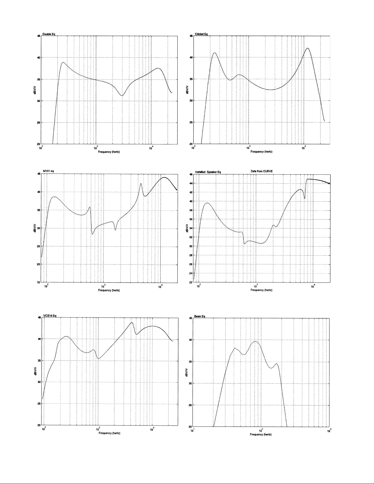
SPEAKER EQ CURVES
CS-2 Satellite Speaker EQ Curve Jewel Cube® Satellite Speaker EQ Curve
Residential 131® Satellite Speaker EQ Curve
VCS-10® Center Channel Speaker EQ Curve
Residential 1.2 Ohm Speakers
EQ Curve
Acoustimass® Series II Bass Module
EQ Curve
4
Page 5

General Overview
THEORY OF OPERATION
The Bose® Digital BUILT-INvisible® amplifier is a six-channel system with DSP-based Dolby
®
Digital 5.1 decoding and Videostage® II signal processing. It is intended for built in installations in
Bose residential sound systems. Its six channels will normally be presenting sound for home
theater, in 5.1 format.
The Digital BUILT-Invisible amplifier has a total of six audio inputs:
- stereo analog audio for a music source
- stereo analog audio for a video source
- four digital audio for stereo or multi-channel Dolby Digital 5.1 audio (SPDIF coax)
Furthermore, the Digital BUILT-Invisible amplifier has a number of control ports:
- Lifestyle® music center compatible input
- RS-232C serial bi-directional port
- TV Sensor input
- Remote IR sensor input
- IR diode
The amplifier responds to the various SmartSpeaker commands issued from the various Bose
Lifestyle
®
head-end units, such as the CD-5, CD-20 and the PMC/MRI used with the Lifestyle
®
40 and 50 systems. The amplifier can also be controlled via an external master remote control
(Philips) used in conjunction with either the CI-1 Control Integrator or the SE-1 Expander.
The Digital BUILT-Invisible amplifier is packaged in a metal enclosure, consisting of a steel base
and an aluminum extrusion cover. Internally, the electronics consist of:
- Input/Output (I/O) PCB
- Power Amplifier PCB
- DSP (Digital Signal Processor) PCB
- Toroidal power transformer
Input/Output (I/O) PCB
Note: Unless otherwise noted, refer to the schematic diagram for the Input/Output board for the
following information. The references in brackets [ ] are the grid coordinates for the component.
Analog audio inputs
The audio signals are applied at J6 [A4] and J21 [A3]. J6 is used for Music Audio Inputs and J21
is used for Video Audio Inputs. U1, 2, 7, & 8 [A2-4], dual op amps, comprise the four differential
amplifiers for these inputs. Each differential amplifier uses two op amp sections. The non-inverting (+) input passes through two inverting sections, while the inverting (–) input passes through
only the second inverting section. In this way, the amplifier responds to the difference between
the non-inverting (+) input and the inverting (–) input. External signals appearing in common on
the two input pins (capacitively or inductively coupled noise) are subtracted and are largely
eliminated. To improve common mode rejection, the critical resistances are packaged in a precision thin film network RN1 [A4] with a high degree of matching. To protect the differential amplifier
against ESD and the presence of higher than normal audio signals with or without power
present, series resistors R105 and R106 [A4] and D25 and D26 [A4] provide clamps. Further
ESD protection comes from the spark gap PCB patterns. C3 and C5 [A4] provide low pass
filtering to remove RF that could be picked up by input wiring.
5
Page 6

THEORY OF OPERATION
Input/Output (I/O) PCB (continued)
S1 [A3] section 1, a user accessible switch, is used to connect the left and right inverting (–)
pins of the Music Inputs together. S1-section 2 is used to connect the left and right – pins of the
Video Inputs together. This is sometimes desirable for certain installation wiring situations, such
as where the source wiring presented to the TA-1 amplifier is left non-inverting (+), right +, and a
common ground (unbalanced). One might choose to close S1 and connect left + to left +, right +
to right +, and common ground to left – (S1 will tie left – to right – in this case).
Analog audio input selector
The two stereo inputs, Music Audio and Video Audio, after passing through their differential
amplifiers, are presented to U3 [B4], an analog multiplexer at pins 4, 5, 12 and 13. When the
Set_Audio (U3 pin 1) input is high, the Video Audio input is selected and passes through. When
the Set_Audio line is low, the Music Audio input is selected. From U3’s outputs at pins 8 and 9,
the analog audio signals pass to J4-12 and 14, which carries them onto the DSP PCB, where
they enter the codec U100, [DSP schematic sheet 1, C4] and are converted to digital audio
signals.
Digital audio inputs
The four S/PDIF digital audio signals are delivered via J7 [C3], each in differential form. A typical
S/PDIF source, Source 1, is presented on J7-4 and J7-5 and passes through a DC blocking
capacitor (to keep the small transformer free of a DC bias) and into T1 [D3]. At the secondary,
the transformer is terminated in 75 Ohms to match the source impedance for best pulse fidelity.
Also at the secondary, the signal is referenced to ground and clamped to about +/-0.65 volts by
diode D8. The clamp is only active for higher than normal S/PDIF sources, but also protect the
inputs of U9 [D3], especially if signals are present while the power is off.
Digital audio input selector
The four single-ended digital sources are presented to U9 [D3], an analog multiplexer. Signals
DIG_SEL_A and DIG_SEL_B from the microcontroller U5 [C4] select one of the four inputs for
passage through U9. Signal DIG_EN can be used to disable the output regardless of the source
selection. From U9’s output, the selected SPDIF signal passes to J4-8 [E4], which carries it onto
the DSP PCB, where it enters a codec U100, [DSP schematic sheet 1, C4] and is unpacked to
yield the embedded digital audio signals.
Power amplifier outputs
The power amplifier output devices U700, U701, U703, U704, U705 and U707 (and associated
power transistors) [amplifier PCB schematic sheet 1] are located on the power amplifier PCB
which is attached to the extruded top cover. The amplifier output signals and their ground returns
are carried via a wire harness from J701 [power amp schematic sheet 2, A-C7] on the amplifier
PCB to J22 [D2] on the I/O PCB. The six amplifier outputs are directly wired to the appropriate
loudspeaker connectors along the right hand edge of the PCB. The RC networks [E2] contribute
to amplifier stability and reduce EMC and ESD events.
Power supplies, +8V and +5V
The I/O PCB receives the AC mains power via J5 [C2] and S9, and through fuses F3 and F4.
The +8V and +5V supplies provide keep-alive voltages to the I/O PCB control circuitry that
enable the amplifier to remain in standby mode, but also allow it to wake up and go into operate
mode when it receives commands to do so. When main power switch S9 is on, the +8V and +5V
supplies are energized. At first, the amplifier will be in standby mode, characterized by the
presence of +8V and +5V, but with the triac Q6 [C1] off.
6
Page 7

THEORY OF OPERATION
Input/Output (I/O) PCB (continued)
Power supplies, +8V and +5V (continued)
Until Q6 is turned on, the rest of the amplifier (the Power Amplifier and DSP PCBs) is off.
The AC mains is applied to T5 [C1], rectified by D22 (full wave bridge), and filtered by C31.
The +5V supply is created by U12 [C1] in a standard 3 terminal regulator application; so too is
+8V, created by U14. These supplies only deliver very low power outputs, capable of no more
than two to three watts total.
Power supply, main transformer control
The amplifier’s main power supply is created from the secondaries of a large toroidal transformer
that is turned on and off by the triac Q6. This is the transformer mounted in the center of the I/O
PCB. The secondary leads of this transformer connect via J702 to the Power Amplifier PCB,
where various power supply voltages are created, including the +/-12V supplies returned to the
I/O PCB to power the op amps and signal selectors. The +/-12V leave the amplifier PCB at J701
pins 13 and 15 and enter the I/O PCB at J22 pins 13 and 15.
A logic signal (AMP_POWER) from the microcontroller U5 [C4] at pin 11, goes high to turn on
the main power supply. AMP_POWER high causes base current in Q7 [C1], which in turn
causes the LED in Q5 to turn on. The opto-coupled LED turns on the internal triac in Q5 which,
finally, turns on the gate of triac Q6 and energizes the transformer.
Pulse Width Modulated tone control low pass filters, U15
The I/O PCB interprets user commands to change the bass and/or treble levels by delivering an
analog voltage between 0V (cut), +2.5V (flat), and +5V (boost) to the DSP PCB. The microcontroller U5 develops this analog voltage by controlling two of its output pins in pulse width
modulation mode. The inherent switching activity in PWM outputs requires a low pass filter, in
this case a 2
Clamp diodes D36 and D38 on the op amp outputs keep the filter output within bounds for its
destination, the DSP microcontroller U202 on the DSP PCB. The signals TREBLE and BASS
are passed to the DSP microcontroller U202 via J4-1 and J4-2 [E4].
TV Sensor input
J11 [A1], a three pin connector, provides ground and +8V (via resetable fuse F2 [A1]) for use by
a small TV sensor that must be attached to the TV monitor in the home theater. The TV sensor
circuitry returns a DC signal via J11-1 which, when high, indicates that the TV set is on. This will
cause the amplifier to turn on (if it is not already on). The TV sensor input is monitored by
microcontroller U5 [C4] at pin 8.
IR input
J10 [A1] acts as the gateway for incoming demodulated IR signals used by remote controls.
These signals are ultimately monitored by the microcontroller U5 [C4] and are sent to the DSP
PCB at J4 [E4]. One form of IR delivery is the electrical signal (logic level) from an externally
mounted IR receiver chip. This would typically be located in the home theater room, where it
would pick up IR radiation from a user remote control, decode it, and send it by wire to J10-3.
This signal is clamped and sent to AND gate U16 [B1], which acts as an OR selector for low
levels coming from this IR input and from the internal IR sensor. The second form of IR delivery
is via an electrical signal sent to J10-1 and –2. When this signal is asserted, the internal IR
emitter D3 [A1] is turned on and emits IR within the amplifier. This optically couples to IR sensor
U11 [A1] which toggles low and high, decoding the IR signal. This signal passes to U16’s second
input, where it is OR’d with the IR source discussed above. Finally, the IR signal is sent to the
microcontroller U5 [C4] as the signal IR_IN on U5 pin 7.
nd
order filter consisting of passive components and the dual op amp U15 [C2].
7
Page 8
THEORY OF OPERATION
Input/Output (I/O) PCB (continued)
Music Center input
®
J8 [A1], a four pin connector, provides a connection from a Bose
Lifestyle® music center to the
amplifier. This connector serve two functions. It can be used for connection to a Bose Lifestyle
music center or alternately for remote terminal access by means of an IBM compatible PC.
A table will help explain this.
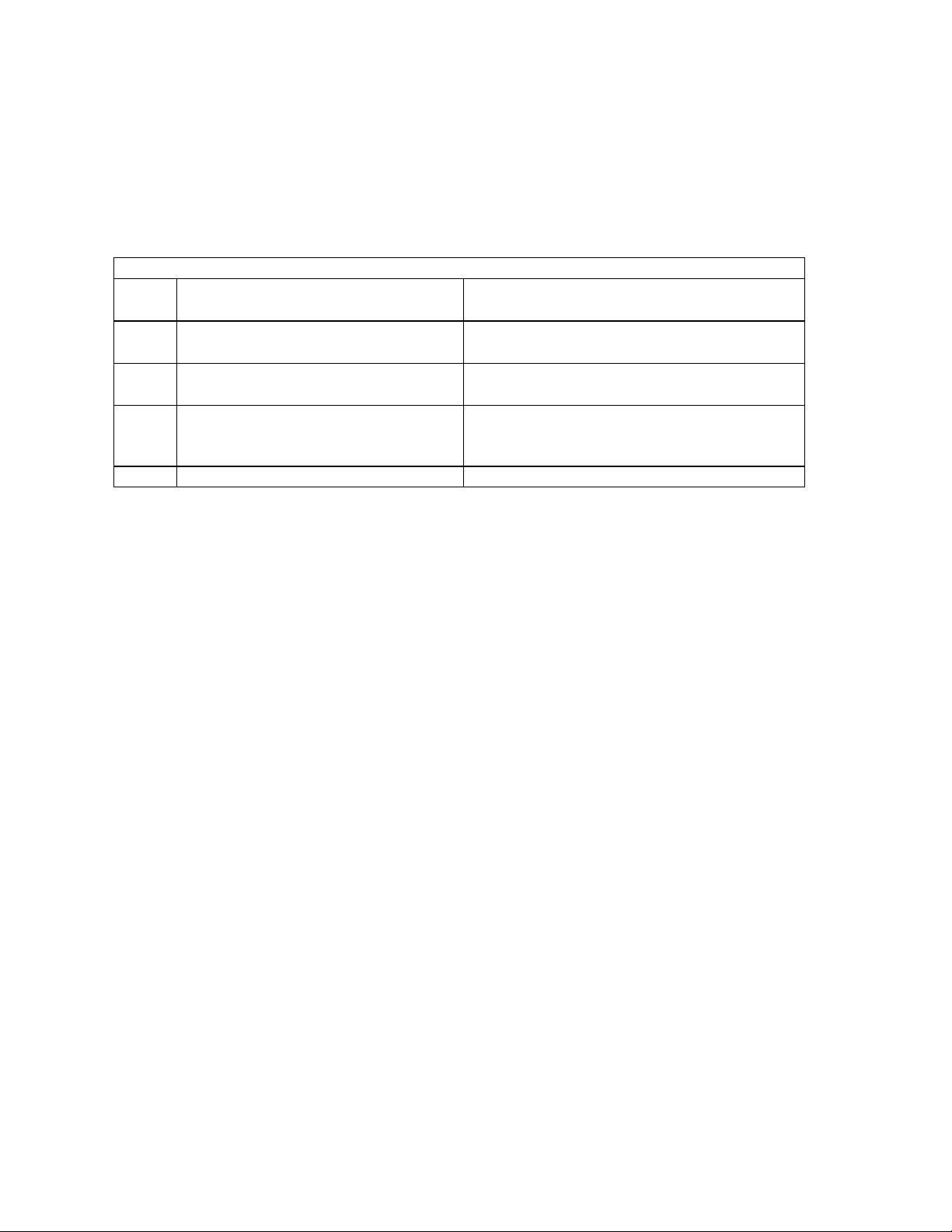
J8 Functions
J8
pin
1
2
Mode: Normal Lifestyle
connection
Turn_on signal from Lifestyle
the amplifier
Speaker data sent from Lifestyle
to the amplifier
to
Mode: Remote terminal access
RS-232 RX line, data sent from RS-232C
terminal or PC to the amplifier
RS-232C TX line, data sent from the
amplifier to RS-232C terminal or PC
3 Antenna signal DTR: RS-232C terminal or PC sets this
high to tell the amplifier to operate in the
Remote Terminal Access mode
4 ground reference ground reference
In the Remote Terminal Access mode, a system installer can set up a notebook PC in the home
theater room and run InstallerTM software to custom equalize and balance the amplifier system
for the customer’s particular home theater room. The installer would connect the PC’s RS-232C
serial output to the Lifestyle® connector on the Bose wall panel, temporarily disconnecting the
Lifestyle® music center. Switching between the two modes is accomplished via the DPDT relay
K1 [A1]. K1, shown in the deenergized state (Normal Lifestyle® mode), is controlled by the logic
level signal provided to pin 3 when the remote terminal is present and has activated DTR.
®
RS-232C input/output
The amplifier in some installations may work entirely under RS-232C control. Such installations
may have Crestron or AMX remote control devices. J9 [A2] provides for RX, TX, and ground
connections to such a terminal. Since RS-232 sources can present electrical waveforms swinging between up to +/-12V, the RX signal is passed through a special RS-232C to TTL translator,
part of IC U10. In the same fashion, to permit the amplifier to transmit a bipolar TX signal, the TX
source is buffered on the way out through the output section of U10.
S4, Speaker EQ switch, and J1, Header to Test Accessory
The four signals controlled by S4 [B3] are read by the microcontroller U5 [C4] during initial
power-up of the amplifier. Refer to the Appendix of this manual for the EQ settings of S4.
J1 connects the I/O PCB with the test accessory. This connector is not used on production
amplifiers.
8
Page 9

THEORY OF OPERATION
Input/Output (I/O) PCB (continued)
Power supply failure monitor level translator
There are four power supplies on the power amplifier PCB, derived as two pairs of symmetrical
bipolar supplies. By tying each of these supplies into a node by appropriate resistor values, we
have a node that sits at zero volts when all supplies are normal. If one or more supplies deviates
sufficiently, we want to detect this as an error. The node PROTECT is brought out of the amplifier
PCB at J701 pin 11 [amplifier sheet 2, A7] and onto the I/O PCB at J22 pin 11 [D2] and connects
to Q1 and Q2 [D2]. Q2 turns on when PROTECT exceeds about 0.5V, while Q1 turns on when
PROTECT exceeds about –0.5V. This dual transistor’s output (Q1 collector) is normally high,
reflecting the state where all six power supplies on the power amplifier PCB are within normal
limits. When either transistor turns on, the output signal BUF_PROTECT_N out of Q1 goes low,
indicating a failure. The PROTECT signal also becomes active when there is a DC offset failure
in the bass speaker amplifier.
When the PROTECT signal becomes active, the microcontroller (U5) [C4] on the I/O PCB
responds by placing the unit into the Standby state, where the main power transformer is deenergized. The Fault LED D29 [D4] flashes on and off when this occurs. The next time a user
command is issued, it attempts to turn on, and will stay on if the fault has been cleared; otherwise, it will again switch to the Standby state.
Microcontroller U5 and related circuits
The I/O PCB requires its own microcontroller to monitor the serial interfaces, the installer DIP
switches, the TV sensor, etc. It is responsible for passing along control commands to the
microcontroller U202 [DSP schematic sheet 2, C5] on the DSP PCB. The I/O PCB’s microcontroller U5 is clocked internally by an oscillator using the crystal Y1 [C3]. The microcontroller
can write and read to the optional (not installed) EEPROM U6 [C3]. A reset generator U4 [C4]
ensures that the microcontroller wakes up and executes its reset routine when power is turned
on or momentarily interrupted. The microcontroller handles the 3 LEDs [D4] Command (D28),
Fault (D29), and Setup (D30). It also reads the configuration DIP switches contained in S7 [D4],
as well as the speaker EQ switches S4 [B3]. Other functions (bass and treble PWM outputs,
etc.) have been mentioned elsewhere in this presentation.
Digital Signal Processor (DSP) PCB
Signal Processing
Note: Unless otherwise noted, refer to the schematic diagrams for the DSP board for the follow-
ing information. The references in brackets [ ] are the schematic sheet and grid coordinates for
the component.
The Digital BUILT-INvisible
PCM (digitized 2-channel audio) or the AC-3 output from up to four separate digital sources.
AC-3, also known as Dolby® Digital, is a perceptual coding and data compression technique that
allows 5 wideband channels and one low frequency bass channel (5.1) to be compressed into
less bandwidth than would be required for 2-channel PCM.
®
amplifier has the ability to receive a digital S/PDIF bitstream, either
The Videostage® 5 processing used in the amplifier expands a L, R input pair into L, C, R, S
and bass, but adds a few new features over previous versions of Videostage, such as stereo
surround channels and a mono to 5 channel mode. The mono to 5 channel mode is a way of
processing a mono soundtrack such that all 5 speakers receive parts of the signal. The amplifier
will also accept two analog inputs directly at the input jacks.
9
Page 10

THEORY OF OPERATION
Digital Signal Processor (DSP) PCB (continued)
Power Supplies
There are several sets of internal power supply voltage rails. These voltages originate with the
main power transformer located in the center of the Input/Output (I/O) PCB. There is also a small
keep-alive transformer T5 [I/O PCB schematic, C1] located on the I/O board itself that allows the
amplifier to be turned on by SmartSpeaker commands.
The power amplifiers are supplied with both +40 and +20 VDC unregulated rails, as determined
by the Class G circuitry. These rails are developed from the transformer secondaries diode
bridges B700 and B701 [amplifier schematic sheet 2, A/B 3/4] and their associated capacitor
banks.
The digital circuitry on the DSP PCB requires two different regulated voltages, +5V and +3.3V.
The +5V regulator U1 [sheet 1, A5] is a standard 3 terminal linear regulator in a surface mount
package and is located on the DSP PCB. It’s powered from the +20V rail via fusing resistor
R704 [amplifier schematic sheet 2, C6] on the amplifier PCB, and supplies about 120mA to the
DSP PCB, most of which is consumed by the microcontroller and codec.
The +3.3V regulator U500 [sheet 4, D4] is a switch-mode regulator and must be located under
the shield to avoid EMI problems (harmonics of the 100 kHz switching frequency will stray into
the AM broadcast band if left unshielded). This regulator is also powered from the +20V rail and
supplies about 350mA to the DSPs.
Operation of the 5V linear regulator is very simple. Current is supplied to the regulator via surface-mount power resistors R10 and R11 [sheet1 A5], which drop the voltage supplied to the
regulator to avoid excessive power dissipation. The regulator needs a minimum of about 7V at its
input terminal to stay in regulation and it should be able to do this even as the +20V rail sags to
+10V or so.
Operation of the +3.3V switch-mode regulator is more complicated. In its simplest terms, the
unregulated input is “chopped” at about 100 kHz, and the resulting pulse train is low-pass filtered
to extract the DC. This DC output is compared to a +3.3V reference, and the duty cycle of the
switching waveform is adjusted accordingly. The high-side switch (the switch that connects
+20V to the output filter) is integrated into the controller, while the low-side switch (the switch that
connects ground to the output filter) is an external diode D500. When the controller is running,
you should be able to observe the switching waveform at L500.
Microcontroller
The microcontroller U202 on the DSP PCB is used for the following housekeeping and
control functions:
to interpret SmartSpeaker commands from the head-end.
to interpret special test mode commands from the functional tester.
to store and retrieve data from nonvolatile memory (U201).
to boot and reprogram the codec (U100) as required by the operating mode of the system.
- to monitor for bass and treble PWM voltage level from U15 on the I/O board.
- DC offset on the amplifier outputs.
- PCB over-temperature.
- presence/absence of a digital S/PDIF signal.
10
Page 11

THEORY OF OPERATION
Digital Signal Processor (DSP) PCB (continued)
Microcontroller (continued)
to sequence the amplifier and codec mute lines as required.
to boot and monitor the performance of the DSPs.
and relay information to/from DSPs.
In detail:
1. SmartSpeaker commands are interpreted by watching for digital activity on the serial data
input line (J5, pin 12 [sheet 1, C8]). This serial input can be either the “standard” SmartSpeaker
protocol, compatible with the outputs of CD-5, CD-20, etc., or it can be 4800 baud RS232 with
5V logic levels. The microcontroller decides which protocol to use based on the voltage level
present on the serial data input at boot time. If the line is low, it assumes RS232; if the line is
high, it assumes SmartSpeaker. It checks only once, at boot time, so switching from one protocol to the other requires a power cycle to reboot the system.
2. Test mode commands are special commands to facilitate testing, or to retrieve stored information from the nonvolatile memory. Test mode commands are RS232 only, e.g., the revision of the
firmware can be queried by sending the command “tv”, the answer “2200/2000” might come
back on the serial data output line. This would indicate version 22.00 for the microcontroller and
version 20.00 for the DSPs.
3. The nonvolatile memory is used to store the following information:
choice of equalization curve.
system, center, and surround volume settings at power-down.
US or Euro bass tone control preference.
system usage statistics.
number of times system was powered off.
minutes spent powered on.
4. The codec U100 [sheet 1, C4] has a fair number of internal registers, all of which must be set
up properly for correct operation, e.g., to switch between the ADC inputs and the S/PDIF input
(both functions are integrated into the codec), the codec must be reprogrammed. In addition,
there are a number of error status bits which are periodically sampled by the microcontroller, the
codec can be rebooted if problems are discovered.
5. The tone control potentiometers are not used on the Digital BUILT-INvisible
bass and treble are adjusted by means of pulse width modulation as acheived with the I/O board
microcontroller and support circuitry. See the I/O board theory of operation for a complete
description. The DSP microcontroller has several ADC inputs, two of which are used to detect
the voltage used to adjust the bass and treble. Everytime this voltage changes it is presented to
the DSPs, which adjust their tone control filter coefficients accordingly.
®
amplifier. The
11
Page 12

THEORY OF OPERATION
Digital Signal Processor (DSP) PCB (continued)
Microcontroller (continued)
6. Other ADC ports are used for the following functions:
• To monitor the gross DC offset on the five satellite speaker channels. Excessive DC offset is
assumed to be an indication of a serious problem and the microcontroller will respond to this
by shutting off the power to the amplifier.
• To detect the presence or absence of a digital S/PDIF signal. The codec cannot be set up for
an analog input and a digital S/PDIF input simultaneously and it cannot be reprogrammed
from analog to digital (or vice versa) without interrupting the audio signal.
• To sequence the mute line. As with the Series I, there are three so-called “speaker modes”,
2-channel (bass, left, right); 3-channel (bass, left, right and center) and 5-channel (bass, plus
all 5 satellites). Unused output channels are muted, not only at the DSP but also at the power
amplifier. The mute inputs to the power amplifiers are 5V logic-level outputs from the
microcontroller.
• The microcontroller is in charge of booting the DSPs at power-up in the following
sequence:
- Boots the codec and establishes the correct output signals from the codec (bit_clock,
frame_clock, and data).
- Enables the 3.3V power supply, and verifies the correct voltage from it.
- Releases the DSP reset line and waits for the DSPs to boot and acknowledge.
The microcontroller is always engaged in dialogue with both DSPs. If the DSPs should fail to
respond within a certain time-out, it is assumed that the DSPs have “crashed” and the DSPs are
rebooted. The microcontroller must pass some of the nonvolatile information in the EEPROM
over to the DSPs at boot time, e.g.: speaker eq, system volume (all volume control in is done in
the DSPs), center and surround volume and bass and treble pot position. The microcontroller
itself can be reset in two ways, by a hardware reset signal, which is generated by U200 when
the 5V supply drops below 4.75V and by the microcontoller itself, once it has already booted
successfully (it can pull its own reset line if the 8 MHz clock is running).
Codec
The codec U100 [sheet 1, C4] is a highly integrated device which includes the following
functions:
•An I 2 C interface for control and status information.
• Three channels of 20-bit ACD; only two are used, one for the left analog input and one for
the right. The ADCs will input signal levels in excess of 1 Vrms.
• Six channels of output DAC; all six are used. Maximum output signal level is 1 Vrms.
• A crystal oscillator which establishes the ADC/DAC sampling rate, in this case, it is
11.2896 MHz / 256 = 44.1 kHz.
• A S/PDIF receiver. “S/PDIF” stands for Sony/Philips Digital Interface Format. Essentially, for
every pair of 20-bit audio samples, another 24 bits of status, parity-checking and general
housekeeping bits are sent along for the ride. The data is encoded in such a way that:
a) there is no net DC content to the bit steam, allowing transformer or AC coupling and
b) the bit clock can be recovered from the bit steam.
12
Page 13

THEORY OF OPERATION
Digital Signal Processor (DSP) PCB (continued)
Codec (continued)
The codec generates three output signals, either from the 11.2896 MHz crystal, or from the input
S/PDIF bitstream;
• a serial bit stream containing the 20-bit audio data.
• a bit_clock, which indicates when to sample the serial bit stream.
• and a frame_clock, which indicates the start of an audio sample.
In addition, there is a serial data input (6 20-bit audio samples) to the codec, with timing that
corresponds exactly to the timing of the serial data output. These four signals (data out, data in,
bit_clock, and frame_clock) are used by the serial ports on the DSPs. The timing of the data flow
into and out of the DSP subsystem is driven entirely by the codec; the serial ports on the DSP
run asynchronously to the 40 MHz clock which drives the DSPs.
DSPs
The DSPs [DSP1, sheet 3 C/D7; DSP2, A/B7] are Analog Devices 21061L general purpose
floating point digital signal processors, each capable of about 40 MIPs of performance.
Two are required to provide enough MIPs for:
• AC-3 decoding.
• Videostage®.
• bass management.
• six channels of speaker equalization.
• tone controls.
The DSPs have no internal ROM; at boot time they load themselves from the external PROM
U401 [sheet 3, C2]. This boot process is more or less automatic; i.e., no intervention from the
microcontroller is required (although the microcontroller has control of the DSP reset line).
The 21061L processors are designed to be bussed together, which accounts for the relatively
large number of pins found on each DSP (240).
For instance, the signals required to connect the DSPs to each other and to the boot PROM
include:
• an external data address buss (32 bits, of which 24 are used).
• an external data buss (48 bits, of which 16 are used).
• buss control signals (buss priority, address and r/w strobes, etc).
Also, there are 30 power and 30 ground pins on each DSP, and a 40 MHz clock oscillator (U400,
crystal CR400, and associated components) which drives both processors.
13
Page 14

THEORY OF OPERATION
Digital Signal Processor (DSP) PCB (continued)
Signal Path
The signal path through the system takes the following route(s):
For analog signals, the L/R stereo pair is introduced from the source via the input cable from the
Input/Output board and the 14-pin connector J9 [schematic sheet 1, A-D8]. Each signal is
received pseudo-differentially by op-amp U105 [B/C6] and associated components and -6 dB of
gain is applied to match with the maximum in/out signal level of the codec (1Vrms).
Digital S/PDIF input signals enter the DSP board at J9 pin 10 [B8] (which come directly from a
S/PDIF signal source selected from one of four possible inputs on the I/O board), the signal is
routed directly to the codec U100 [C4] via a network of components (D1 [B5] and surrounding)
designed to clamp and filter ESD transients.
The codec takes in either the pair of analog inputs, or the single S/PDIF digital input, and outputs
three digital signals (data, bit_clock, and frame_clock, as described earlier). Since the codec
runs on 5V and the DSPs run on 3.3V, any signals passing between them must be level-shifted
via the buffers U101 [D5] and U102 [D3].
Without going into a lot of detail, DSP1 handles (mostly) Dolby® Digital (AC-3) decoding and
Videostage® 5 processing and DSP2 handles (mostly) equalization. With the signal processing
complete, DSP2 formats the six output channels into a single serial bitstream and sends this
back to the output side of the codec U100. The analog buffers following the codec (U103, U104
and associated components) do three things:
• Remove the 2.3VDC reference voltage from the codec’s outputs. The codec is a
single supply (+5V) device and references any of its internal analog signals to a
reference voltage at approximately 2.3V, about one-half the +5V supply voltage.
• Reference the signal to the amplifier ground, not the local ground. The power amps are single
ended and are referenced to their own local ground on the amp PCB, which is not the same
as the local ground at the codec on the DSP PCB. Amplifying the differences between the
two grounds will produce audible hum in the output speakers.
• Provide enough gain to increase the output signal for output to the amplifier board.
The signals leave the codec itself at about 1Vrms full-scale, this is amplified up to about
6Vrms full-scale by the output buffers.
Power-Up Sequence
At power-up, all of the microcontroller ports are in a high impedance state, which means that:
• The amplifier mute lines are held low, muting the power amps.
• The 3.3V regulated supply is disabled, reducing the demand on the +20V supply until
things have stabilized.
• The DSP reset line is held low, holding the DSPs in reset.
14
Page 15

THEORY OF OPERATION
Digital Signal Processor (DSP) PCB (continued)
Power-Up Sequence (continued)
The microcontroller proceeds to:
• Set up its I/O ports.
• Print out a “reset” message on the TTY output.
• Program the codec and verify that it responds.
• Retrieve system variables from nonvolatile memory and print out the “power_cycle” and
“eq” variables.
• Boot the DSPs, and wait for them to respond.
• Pass over system variables to the DSPs.
• Print out any appropriate error messages.
• Unmutes the power amplifiers, then unmutes the DSPs.
At this point, normal signal processing commences. It should take no more than 1.5 seconds
from the time power is applied until the time audio appears at the speaker outputs.
Power-Down Sequence
Upon receiving the “off” command from the head-end, the microcontroller;
• Mutes the DSPs.
• Mutes the power amplifiers.
• Powers down the codec and the DSPs.
• Stores system variables in EEPROM.
And then monitors the voltage level at the turn-on input. When it sees a low to high transition, it
resets itself as if the power had just come on.
Detailed Theory of Operation (see schematic diagram SD256431)
Digital Signal Processor (DSP) Board, Sheet 1 of 4
Sheet 1 of 4 shows the analog input buffers, codec’s power supply, analog output buffers and
some “glue logic” around the codec. The analog input buffers consist of op-amp U105 [B/C6] and
associated components. The ratio of R102 (and R107) to R100 sets the gain; -6 dB from J9 to
the input of the codec. The dual-diodes D100 [D7], D102 [C7], and D104 [B7] are there to clamp
ESD discharges into J9. The filter capacitors C100 [D7], C105 [C7], etc., are present to filter off
RF picked up by the input cable.
The output signal from the buffer is ground referenced, but the codec’s analog inputs are biased
at about 2.3V. C104 [C6] is required to AC-couple the signal from the buffer into the codec. R103
and D103 are present to prevent transients from the op-amp (±12V rails) from overdriving and
perhaps damaging the codec (5V rail). R104 and C102 [C6] are an EMI filter to prevent any RF
leaking from the codec from getting outside the metal EMI shield. The codec is located under the
shield, while the input buffer is not.
15
Page 16

THEORY OF OPERATION
Detailed Theory of Operation (see schematic diagram SD256431)
Digital Signal Processor (DSP) Board, Sheet 1 of 4 (continued)
The S/PDIF input enters the DSP board at J9 pin 10 [B8] and is routed to the codec by means of
C151, R1, R2, D1, C1, C7 and R5 [B5]. C151 AC couples the digital S/PDIF signal, and R1
terminates the input with 75 Ohms. R2 and D1 clamp the input (a typical S/PDIF input is about
500 mVpp into a 75 Ohm load). C1 AC couples the signal at D1 (which is ground referenced) to
the codec input (which will be biased at about 2.3V when the S/PDIF receiver is working). R5
and C7 are an EMI filter designed to prevent RF from leaking outside the shield.
The codec’s power supply consists of U1 [A5] and associated components. R10 and R11 are
power resistors designed to drop the voltage at the voltage regulator’s input, for reducing the
power dissipation of the voltage regulator itself.
D2, D3, and R4 [A5/6] are used to draw a little current from the +12V regulated supply when the
power supplies start to sag severely, as they will at low AC line and heavy amplifier load. The
+12V regulator is fed from the +40V unregulated supply and has considerably more headroom
than the +5V regulator fed from the +20V supply. Also fed from the +20V supply is the 3.3V
switching regulator, which tends to draw more current as its input voltage drops (it delivers a
fixed amount of power, at a fixed conversion efficiency). So, as the +20V supply starts to sag,
the current load on it actually starts to increase, which tends to make it sag more.
The +5 volts supplied by the regulator is sent to two different components; the codec U100 [C4]
and the microcontroller U202 [sheet 2, C5] and associated components. Since the regulator is
located outside the EMI shield and the +5V supply line might be carrying EMI (Electro Magnetic
Interference), ferrite beads L1 and L2 [A4] were placed in series with each of the supply lines.
L1 and R3 [A4] serve to isolate the two different power supply pins on the codec (the “analog”
+5VA from the “digital” +5VD). C5 and C6 are bypass capacitors placed directly under the
codec.
Codec glue logic
U101 [D5] is a 74LCX244, a 3.3V IC that can tolerate 5 volts on its inputs. It’s used to convert
5V to 3.3V logic signals.
U102 [D3] is a 74ACT244, a 5V part that understands the logic levels used by the 3.3V IC. It’s
used to convert the 3.3V logic signals to 5V logic signals.
U106 [A7] is a flip-flop, used to convert a falling edge (from the codec) to a narrow pulse (to the
DSP). This removes a potential timing ambiguity.
R192 [D6] (and others) is a 75 Ohm series resistor used to series-terminate some of the high
speed logic signals, to preserve edge fidelity at the receiving end.
R6 and R7 [C3] comprise a low performance 5V to 3.3V shifter. Using such large series resistances in the presence of even moderate amounts of stray and input gate capacitance slows
down the signal’s edge, but this particular signal is very low bandwidth.
16
Page 17

THEORY OF OPERATION
Detailed Theory of Operation (see schematic diagram SD256431)
Digital Signal Processor (DSP) Board, Sheet 1 of 4 (continued)
Analog output buffers consists of U103, U104 [B-D2], and associated components. Gain is set
by the ratio of R132 to R131 [D2]; to about 6x. Note that the ratio of R189 to R188 [D2] must
match. Gain of the output buffers = (codec_out - codec_reference) - amp_ground_sense).
Sheet 2 of 4 (microcontroller and associated components)
The bass and treble control signal enters the DSP board at J9 pins 1 and 2 [D8]. This signal is
generated on the Input/Output board and connected to a pair of microcontroller ADC inputs at
U202 [C5] pins 19 and 20. All of these connections are EMI filtered.
Thermistor R207 [C8] is mounted on the topside of the DSP PCB. When the DSP PCB temperature rises to about 70 degrees C, the microcontroller starts turning down the output volume by
programming the codec, effectively controlling the maximum temperature inside the amplifier
enclosure and preventing damage.
R211 [D7] connects the signal “CMOUT” to one of the microcontroller’s ADC ports. CMOUT is
the codec’s 2.3V reference voltage. This voltage is monitored as one of the codec’s “vital signs”,
if out-of-bounds, the microcontroller reboots the codec.
R208 [C8] connects the 3.3V power supply to one of the microcontroller’s ADC ports. The
microcontroller has the ability to turn the 3.3V regulator on and off, thus having the ability to
check that the 3.3V supply is within limits. The microcontroller needs to be able to turn the 3.3V
off at power down to avoid draining the +20V supply faster than the -20V supply. If the upper rails
sag faster than the lower rails, the bass amp will unmute causing a “thump” to be heard (about 5
seconds after power down).
R44 throught R48 [I/O schematic sheet, E2] sum together all the satellite outputs and feeds them
out through J4-5 [I/O sheet, E4] to DSP J9-5 [A7] to one of the microcontroller’s ADC ports at
U202 pin 25. The microcontroller watches for grossly excessive DC offset at any of the speaker
outputs. If DC is detected the microcontroller will shut down the AC power.
U201 [B6] is the non-volatile memory. Read/write access is via the 2-wire serial I2C buss.
U200 [D6] generates a 250msec reset pulse for the microcontroller whenever the +5V supply
drops below 4.75V.
D200 [A5] forms a simple level translator. The CLIP signal is generated on the amp PCB whenever one of the satellite power amplifiers starts to clip. It’s an open-collector output that pulls
down to -12V. D200 level shifts this signal from -12V through +12V, to 0V through 5V. This levelshifted signal goes to both the microcontroller and DSP2 (via a 5V to 3.3V buffer). As it turns out,
the microcontroller ignores this signal, but DSP2 turns down the system volume until the CLIP
signal disappears, then lets the volume drift back up to the original setpoint.
Q204 and Q201 [B3] form a simple S/PDIF detector. Q204 sets the bias for Q201 such that it is
just barely off. An S/PDIF signal arriving at Q201 will cause C216 to be discharged, causing the
voltage at C216 to drop from 5V to something closer to ground. This voltage is connected to one
of the microcontroller’s ADC ports and is sampled periodically by the microcontroller.
17
Page 18

THEORY OF OPERATION
Detailed Theory of Operation (see schematic diagram SD256431)
Digital Signal Processor (DSP) Board, Sheet 2 of 4 (continued)
Q200 [C2] allows the microcontroller to pull down on the DSP’s reset line. When the
microcontroller first boots, all of its output ports are set to a high impedance state. Q200 remains
turned on by R252, which holds the DSPs in reset, until the microcontroller is ready to boot the
DSPs.
R246, R248, [C/D2] etc. connect several of the microcontroller output ports to the MUTE inputs
on the power amplifiers. The mute signals are organized into three groups; (bass, left, right),
(center) and (left_surround, right_surround), corresponding to the three speaker modes the
product supports. Each line is EMI filtered. Pulldown resistors R813, R814 and R815 [amplifier
schematic sheet 2, [D5] guarantee that the signals will assume a LOW state i.e., muted) at
power-up.
Sheet 3 of 4 (DSPs)
There are only two DSPs, but since they each have 240 pins, they’ve been broken into several
different schematic symbols so as not to clutter the page:
- address and data busses.
- buss control, and miscellaneous.
- link ports (sheet 4).
- power and ground (sheet 4).
Without going into any detail, the DSPs are connected to each other and to the boot PROM
U401 [C2], as follows:
- address buss connected to address buss.
- data buss connected to data buss.
- buss control signals connected to buss control signals.
- power pins connected to 3.3V power plane.
- ground pins connected to ground plane.
The large number of interconnects and the fact that each signal has extremely fast rise times
(2 nsec), required the use of a four layer PCB. One of the inner layers is a (more or less) solid
ground plane; the other is used for a power plane, plus additional signal interconnect where
required.
U400 [B2] and associated components form a third-overtone 40 MHz oscillator. There are two
buffered outputs; one drives both DSPs and one is connected to the test connector J401 [B1],
which was used to help debug the prototype PCBs but is no longer loaded.
Sheet 4 of 4
U500 [C/D4] and associated components form a 3.3V regulated supply. C500 and L500 [C5] are
the regulator’s output filter. R500 and C501 [D4] set the regulator’s switching frequency (about
100 kHz). C503 [C4] is the “bootstrap” capacitor required for establishing an internal bias voltage
higher than the supply voltage (for turning on the internal N-channel MOSFET switch). C515,
L501, and C505 [C4] prevent switching harmonics from leaking back out onto the raw DC input
voltage. R501, C507, C508 [C3], etc., are feedback and compensation components.
18
Page 19

THEORY OF OPERATION
Detailed Theory of Operation (see schematic diagram SD256431)
Digital Signal Processor (DSP) Board, Sheet 4 of 4 (continued)
C506 [D3] is the “soft-start” capacitor, which forces the regulator to start up slowly when power
is first applied, thus limiting the inrush current. R510 and Q500 [D3] allow the “soft-start” pin to be
pulled low, shutting off the regulator. The 3.3V supply is turned off as part of the normal power
down sequence.
Detailed Theory of Operation (see schematic diagram SD256421)
Power Amplifier Board
Note: Unless otherwise noted, refer to the schematic diagrams for the power amplifier board for
the following information. The references in brackets [ ] are the schematic sheet and grid coordinates for the component.
Sheet 1 of 2
The satellite channel power amplifiers are a discrete high efficiency Class-G design. Maximum
power is 35 W per channel into 4 Ohms at less than 0.1% THD. In Class-G operation the amplifiers are powered by two different power supplies depending on the amplitude of the signal input.
When the audio amplitude is low, the amplifiers run off of the lower supply rails, but during musical peaks they switch to the higher supply rails. Efficiency is typically increased from 20% to
40% and power dissipation is reduced by a factor of 2.5.
Bass Channel Power Amplifier
Audio input is applied to the amplifier PCB at pin 12 of connector J700 [amplifier schematic sheet
2, D7] and is AC coupled through C727 [D8]. The amplifier is controlled by negative feedback to
op-amp U707 [C6], which is configured as an inverting amplifier with a voltage gain of 12 (21.6
dB). With no signal applied to the input, all output power devices are biased off. For a negative
input signal, pin 1 goes high and conducts driver transistor Q713 [D6]. Collector current is pulled
through R707 and R774 [D6] until the voltage drop across R774 reaches about 1 Volt, at which
time the high gain darlington transistor Q718 [D6] begins to conduct emitter current through
power diode D711 [D5/6], which connects to the +20VDC supply.
Collector current from Q718 [D6] flows through the speaker load and the voltage at this node is
regulated by feedback to the op-amp via resistor R789 [D7].
When the audio output voltage approaches the 20VDC power supply rail, output transistor Q718
begins to saturate and conducts much more base current than the normal maximum of 5mA. At
approximately 8mA the voltage drop across 75 Ohm resistor R707 [D6] exceeds 0.6V and small
signal transistor Q714 [D6] begins to conduct. This in turn conducts Class-G Darlington transistor Q715 [D6], which turns on the 40VDC power supply and reverse biases power diode D711
[D6], effectively turning off the 20VDC supply. During this period, the waveform at the collector of
Q715 resembles the audio output signal plus the saturation drop of Q718 and Q715 is operated
in the active region (not as a switch), thus sharing the power dissipation.
Crossover distortion and switching transients are not an issue due to the relatively low bandwidth of the amplifier (less than 250 Hz) and the ability of the bass module to roll off high frequency distortion products. Crossover distortion is less than 0.5% at 200 Hz, 1 Watt.
19
Page 20

THEORY OF OPERATION
Detailed Theory of Operation (see schematic diagram SD256421)
Power Amplifier Board, Bass Channel Power Amplifier (continued)
Short circuit protection is provided through current sense resistor R822. At greater than 16A,
Q726 conducts and triggers the one-shot op-amp circuit U707, pins 5, 6 and 7, and mutes the
amp for several seconds. The amp will cycle in and out of mute until the short circuit is removed.
Satellite Power Amplifiers
Each of the five satellite amplifiers are operated in Class-G configuration and consist of a 50W,
Class AB monolithic integrated circuit (in a multiwatt-15 package, TDA7294). The amplifier is
short circuit and thermally protected. External to this IC is a pair of TO-220 Darlington transistors
(the same as used in the discrete bass amplifier) to perform the Class-G power supply switching. The following detailed operation is described for the left surround channel, however the other
four channels would be the same.
The surround signal enters the amplifier board at J700 pin 11 [sheet 2, D7] and is applied to
capacitor C717 [C5] and couples to the non-inverting input of the TDA7294 amplifier IC. It is
configured as a non-inverting amplifier with a voltage gain of 4 (12 dB). The output stage consists of a pair of MOSFET transistors and the positive FET must develop gate drive well above
the supply voltage and hence there is a bootstrap cap, C716 [C3], between pin 6 and 14.
With low amplitude signal, the amplifier runs off of the 20VDC rails through power diodes D704
[D3] and D710 [C3]. The power supply voltage at pin 13 is subtracted by 5.6V zener diode D703
[D3] and divided down by the ratio of 1 + R731/R732 [D3/4]. This bias voltage sets the threshold
at which transistor Q703 [D4] turns on. When the audio or the input to the amplifier exceeds the
voltage at the emitter of Q703 by two diode drops, D716 [C4] and Q703 conduct. In turn this
conducts small signal transistor Q704 [D4] which in turn conducts output transistor Q705 [D3].
A negative feedback loop is established that prevents Q705 from turning completely on and the
voltage at the collector of Q705 resembles the audio output wave form plus several volts of
saturation headroom. Q705 operating in the active region (instead of as an on/off switch), results
in shared power dissipation between the transistor and the power amplifier IC. The phase lag
created by the input network R753 and C745 [C4] allows the power circuit to switch on slightly
ahead of the power amplifier at high frequencies (above 8 kHz) to minimize turn-on glitch.
Power Amplifier Board, Sheet 2 of 2
Power Supplies and Connectors
AC power is sent to the amplifier board at J702 [A/B5] from the secondary of the power transformer [I/O schematic sheet, D1] located in the center cutout of the Input/Output board. The raw
AC is recitified by bridge rectifiers B700 and B701 [A/B4]. The filtered DC from B701 is passed
through fusible resistors R713 and R714 [B3] and output as +40V fused. These 40V rails are
used as the higher rail voltage for the Class G amplifier output devices as shown on amplifier
schematic sheet 1. The +40Vdc fused outputs are also are regulated down to +12Vdc by regulators U708 and U709 [B/C2]. This +12Vdc is fed to both the DSP board through J700 pins 2 and 6
and to the Input/Output board at J701 pins 13 and 15 [A7]. The filtered DC from B700 provides
+20Vdc and is used as the lower rail voltage for the amplifier Class G output devices.
20
Page 21

THEORY OF OPERATION
Power Amplifier Board, Sheet 2 of 2 (continued)
Outputs to the DSP board from the amplifier board at J700 also include the +20Vdc at pin 4
through fusible resistor R704 [C6] to create +20 fused. The mute and standby signals for the
power amplifiers are brought into the amplifier board at J700 on pins 15, 16 and 18.
The audio inputs to the power amplifier board are applied at J700 [C/D7] pins 8-12 and 14 via a
cable running from J8 of the DSP board. These inputs are then applied to the inputs of the
individual amplifier channels as shown on amplifier schematic sheet 1.
The outputs of all six of the amplifier channels are brought out of the amplifier board at J701 pins
2, 3, 4, 6, 8 and 10. These outputs are fed back to the Input/Output board at J22 by a cable. The
bass channel output is also monitored and output to the Input/Output board as the PROTECT
signal at J701 pin 11. This PROTECT signal is applied to the Input/Output board at J22 pin 11
[Input/Output board schematic, D2]. It is passed to a window comparitor made up of transistors
Q1 and Q2. The output of this comparitor is the signal BUF_PROTECT. This signal is sent to the
microcontroller U5 [C4] at pin 3. In the event of a failure, this BUF_PROTECT signal will cause
the microcontroller to send out a shutdown command on the Amp_Power pin 11 of the
microcontroller to shut down power to the amplifier.
DISASSEMBLY/ASSEMBLY PROCEDURES
Note: Refer to figures 1, 2 and 3 for the
following procedures.
1. Heatsink Removal
1.1 Using a Phillips-head screwdriver,
remove the four screws (20) that secure the
heatsink (16) to the chassis (8).
1.2 Lift the heatsink straight up just far
enough to be able to reach the amplifier
board (9 & 10) cables. Disconnect these two
cables. The amplifier board is mounted to the
underside of the heatsink. Lift the heatsink
clear of the chassis.
2. Heatsink Replacement
2.1 Align the heatsink (16) with the chassis
base (8). Reconnect the two cables removed
in step 1.2. Slide the heatsink down over the
chassis until it is flush with the chassis end
plates.
3. Input/Output Board Removal
3.1 Perform procedure 1.
3.2 Disconnect the two cables that run to the
power transformer (4).
3.3 Using a nut driver, remove the one hex
head bolt (2) that secures the power transformer to the chassis (8). Lift the power
transformer out of the chassis. Lift the power
transformer gasket out of the chassis.
3.4 Using a Phillips-head screwdriver,
remove the four screws (1) that secure the
input/output board (6) to the chassis. Lift the
input/output board straight out of the chassis.
4. Input/Output Board Replacement
4.1 Align the input/output board (6) with the
chassis (8) and secure it in place using the
four screws (1) removed in step 3.4.
2.2 Secure the heatsink to the chassis using
the four screws (20) removed in step 1.1.
4.2 Place the power transformer gasket into
the chassis.
21
Page 22

DISASSEMBLY/ASSEMBLY PROCEDURES
4.3 Align the power transformer (4) with the
chassis and secure it in place using the hex
head bolt (2) removed in step 3.3.
4.4 Perform procedure 2.
5. DSP Board Removal
5.1 Perform procedure 1.
5.2 Disconnect the cable that runs from the
Input/Output board (6) to the DSP board (5).
Disconnect the cable that runs from the
amplifier board (14) to the DSP board.
5.3 Using a Phillips-head screwdriver,
remove the four screws (1) that secure the
DSP board to the chassis (8). Lift the DSP
board out of the chassis.
6. DSP Board Replacement
8. Amplifier Board Replacement
8.1 Place the thermal conducting insulating
tape strips (15) onto the heatsink (16) where
the amplifier board (14) output devices will
be located.
8.2 Align the amplifier board with the
heatsink and secure it in place using the two
standoffs (13) removed in step 7.3.
8.3 Align the tension clamp (12) with the
amplifier board and secure it in place using
the two screws (11) removed in step 7.2.
8.4 Perform procedure 2.
6.1 Align the DSP board (5) with the
chassis (8) and secure it in place using
the four screws (1) removed in step 5.3.
6.2 Connect the cable that runs from the
DSP board to the input/output board (6).
Connect the cable that runs from the DSP
board to the amplifier board (14).
6.3 Perform procedure 2.
7. Amplifier Board Removal
7.1 Perform procedure 1.
7.2 Using a Phillips-head screwdriver,
remove the two screws (11) that secure the
tension clamp (12) to the amplifier board
(14). Lift the tension clamp off of the amplifier
board.
7.3 Using a nut driver, remove the two
standoffs (13) that secure the amplifier
board to the heatsink. Lift the amplifier board
out of the heatsink (16).
22
Page 23

TEST PROCEDURES
Test Setup
Note: The commands used in the following
tests can either be issued by an IR remote
control or PC generated (using hyperterminal) through the RS-232 (TAP) interface
at J9. Refer to the IR commands table in the
appendix of this manual. There is a built-in
remote receiver located on the Input/Output
PCB behind the IR sensor input connector
(J10). If you aim the IR remote at this connector, the IR command will be received by
IR sensor U11. Refer to the Input/Output
PCB schematic sheet for more information.
The following test procedures use TAP
commands issued by an IBM compatible PC.
The TAP commands are used to emulate
commands that would normally be sent by
an IR remote control, with the exception of
the max volume command (S31101), which
is a Lifestyle® Smart Speaker command. To
set the amplifier to full volume using an IR
remote, hold the volume up button for 10
seconds.
Setup instructions for the PC and fabrication
instructions for the TAP cable are located in
the appendix.
Equipment Required:
Audio Signal Generator
S/PDIF Analog to Digital Converter
CAT-5 Cable with RJ-45 connectors
75 Ohm RCA to RCA S/PDIF video cable
Bose® Digital Source plate
IBM Compatible PC w/Windows
TAP Cable
Digital Multimeter
Audio Distortion Analyzer
5 - 8 Ohm, 50 Watt load resistors
1 - 4 Ohm, 150 Watt load resistor
Note: Refer to figures 7 and 8 for the following test setup information.
®
1. Connect the signal generator inputs to the
left and right Music Audio inputs at J6 pins
1, 2, 4 and 5.
2. Place the balanced/unbalanced switches
(S1) to the unbalanced (single-ended)
position. Use a piece of wire to jumper
the negative inputs (J6 pins 2 and 5) to
ground at J6 pin 3.
3. Connect the TAP cable to the amplifiier at
the RS-232 Serial Data Input jack at J9.
Connect the other end to the IBM compat ible PC comm port. TAP cable fabrication
and IBM PC setup are outlined in the
appendix of this manual.
4. Connect an 8 Ohm load resistor to the
satellite speaker channels at J12, J13 and
J14. Connect the 4 Ohm load resistor to
the bass channel speaker output at J15.
5. Set the speaker selector DIP switch (S4)
position 1 to the UP position. Set positions
2, 3 and 4 to the DOWN position. Cycle
the AC mains power to allow this change
to go into effect. This will select the Jewel
Cube® satellite EQ for the following tests.
6. Issue the following commands to the
amplifier under test via hyperterminal.
These commands will put the TA-1 ampli fier into the proper mode for testing.
Note: These commands are case
sensitive.
- ICA (selects music audio inputs)
- I78 (DRC off)
- IF4 (film EQ off)
- IA0 (1-to-5 off)
- IDA (bass boost to mid)
- IB2 (treble boost to mid)
- ID0 (surround mode)
- IF7 (center channel level to mid)
- IF9 (surround channel level to mid)
- S31101 (sets amplifier volume to max)
23
Page 24

TEST PROCEDURES
Music Audio Tests
1. Front Channel Audio Tests
1.1 Set up the amplifier under test as outlined
in the test setup.
1.2 Apply a 100 mV, 1 kHz signal to the left
music audio input at J6 pins 1 and 2.
1.3 Reference a dB meter to the input level.
1.4 Measure the output level at the left front
speaker output at J12 pins 3 and 4. It should
be +34.6 dB + 1.5 dB.
1.5 Apply a 100 mV, 200 Hz signal to the left
music audio input at J6 pins 1 and 2.
1.6 Reference a dB meter to the input level.
1.7 Measure the output level at the left front
speaker output at J12 pins 3 and 4. It should
be +37.1 dB + 1.5 dB.
1.8 Apply a 100 mV, 12 kHz signal to the left
music audio input at J6 pins 1 and 2.
1.15 Apply a 1.8 Vrms, 1 kHz signal to the
left music audio input at J6 pins 1 and 2.
1.16 Measure the compressor signal distortion level at the left front speaker output at
J12 pins 3 and 4. It should be < 2.0%
THD+N.
1.17 Repeat steps 1.2 to 1.16 for the right
music audio input, applying the signal at J6
pins 4 and 5 and measuring the output at
the right front speaker output at J12 pins
1 and 2.
2. Center Channel Audio Tests
2.1 Set up the amplifier under test as out-
lined in the test setup.
2.2 Apply an in-phase, 100 mV, 1 kHz signal
to the left and right music audio inputs at J6.
2.3 Reference a dB meter to the input level.
2.4 Measure the output level at the center
channel speaker output at J13 pins 1 and 2.
It should be +33.7 dB + 1.5 dB.
1.9 Reference a dB meter to the input level.
1.10 Measure the output level at the left front
speaker output at J12 pins 3 and 4. It should
be +39.0 dB + 1.5 dB.
1.11 Apply a 50 mV, 1 kHz signal to the left
music audio input at J6 pins 1 and 2.
1.12 Measure the small signal distortion
level at the left front speaker output at J12
pins 3 and 4. It should be < 0.5% THD+N.
1.13 Apply a 600 mV, 1 kHz signal to the left
music audio input at J6 pins 1 and 2.
1.14 Measure the large signal distortion
level at the left front speaker output at J12
pins 3 and 4. It should be < 0.2% THD+N.
2.5 Apply an in-phase, 100 mV, 200 Hz
signal to the left and right music audio
inputs at J6.
2.6 Reference a dB meter to the input level.
2.7 Measure the output level at the center
channel speaker output at J13 pins 1 and 2.
It should be +37.7 dB + 1.5 dB.
2.8 Apply an in-phase, 100 mV, 12 kHz
signal to the left and right music audio
inputs at J6.
2.9 Reference a dB meter to the input level.
2.10 Measure the output level at the center
channel speaker output at J13 pins 1 and 2.
It should be +39.8 dB + 1.5 dB.
24
Page 25

TEST PROCEDURES
2.11 Apply an in-phase, 50 mV, 1 kHz signal
to the left and right music audio inputs at J6.
2.12 Measure the small signal distortion
level at the center channel speaker output
at J13 pins 1 and 2. It should be < 0.5%
THD+N.
2.13 Apply an in-phase, 600 mV, 1 kHz
signal to the left and right music audio
inputs at J6.
2.14 Measure the large signal distortion
level at the center channel speaker output
at J13 pins 1 and 2. It should be < 0.2%
THD+N.
2.15 Apply an in-phase, 1.8 Vrms, 1 kHz
signal to the left and right music audio
inputs at J6.
2.16 Measure the compressor signal distor-
tion level at the center channel speaker
output at J13 pins 1 and 2. It should be
< 2.0% THD+N.
3. Surround Channel Audio Tests
3.1 Set up the amplifier under test as out-
lined in the test setup.
3.2 Apply a L= -R, 100 mV, 1 kHz signal to
the left and right music audio inputs at J6.
You can do this by inverting the phase of the
right channel input signal from the signal
generator.
3.7 Measure the output level at the left and
right surround channel speaker outputs at
J14. It should be +36.9 dB + 1.5 dB.
3.8 Apply a L= -R, 100 mV, 12 kHz signal to
the left and right music audio inputs at J6.
3.9 Reference a dB meter to the input level.
3.10 Measure the output level at the left and
right surround channel speaker outputs at
J14. It should be +39.2 dB + 1.5 dB.
3.11 Apply a L= -R, 50 mV, 1 kHz signal to
the left and right music audio inputs at J6.
3.12 Measure the small signal distortion
level at the left and right surround channel
speaker outputs at J14. It should be
< 0.5% THD+N.
3.13 Apply a L= -R, 600 mV, 1 kHz signal to
the left and right music audio inputs at J6.
3.14 Measure the large signal distortion
level at the left and right surround channel
speaker output at J14. It should be < 0.2%
THD+N.
3.15 Apply a L= -R, 1.8 Vrms, 1 kHz signal
to the left and right music audio inputs at J6.
3.16 Measure the compressor signal distortion level at the left and right surround channel speaker output at J14. It should be
< 2.0% THD+N.
3.3 Reference a dB meter to the input level.
3.4 Measure the output level at the left and
right surround channel speaker outputs at
J14. It should be +34.5 dB + 1.5 dB.
3.5 Apply a L= -R, 100 mV, 200 Hz signal to
the left and right music audio inputs at J6.
3.6 Reference a dB meter to the input level.
4. Bass Channel Audio Tests
4.1 Set up the amplifier under test as out-
lined in the test setup.
4.2 Apply an in-phase, 100 mV, 100 Hz
signal to the left and right music audio inputs
at J6.
4.3 Reference a dB meter to the input level.
25
Page 26

TEST PROCEDURES
4.4 Measure the output level at the bass
channel speaker output at J15 pins 1 and 2.
It should be +38.4 dB + 1.5 dB.
4.5 Apply an in-phase, 100 mV, 20 Hz signal
to the left and right music audio inputs at J6.
4.6 Reference a dB meter to the input level.
4.7 Measure the output level at the bass
channel speaker output at J15 pins 1 and 2.
It should be +19.1 dB + 1.5 dB.
4.8 Apply an in-phase, 100 mV, 200 Hz
signal to the left and right music audio inputs
at J6.
4.9 Reference a dB meter to the input level.
4.10 Measure the output level at the bass
channel speaker output at J15 pins 1 and 2.
It should be +29.9 dB + 1.5 dB.
4.16 Measure the compressor signal distortion level at the bass channel speaker output
at J15 pins 1 and 2. It should be < 4.0%
THD+N.
5. DC Offset Test
5.1 Set up the amplifier under test as out-
lined in the test setup.
5.2 With no input signal applied, measure the
DC offset level at the front, center, surround
and bass channel speaker outputs at J12,
J13, J14 and J15. It should be < 10 mVdc.
6. Output Noise Test
6.1 Set up the amplifier under test as out-
lined in the test setup.
6.2 Short out the left and right music audio
inputs at J6.
4.11 Apply an in-phase, 50 mV, 100 Hz
signal to the left and right music audio inputs
at J6.
4.12 Measure the small signal distortion
level at the bass channel speaker output
at J15 pins 1 and 2. It should be < 0.5%
THD+N.
4.13 Apply an in-phase, 230 mV, 100 Hz
signal to the left and right music audio inputs
at J6.
4.14 Measure the large signal distortion
level at the bass channel speaker output
at J15 pins 1 and 2. It should be < 0.2%
THD+N.
4.15 Apply an in-phase, 600 mV, 100 Hz
signal to the left and right music audio inputs
at J6.
6.3 Measure the A-weighted output noise
level at the left and right front and center
channel speaker outputs. It should be < 3.0
mVrms.
6.4 Measure the A-weighted output noise
level at the surround channel speaker
outputs. It should be < 330 uVrms.
6.5 Measure the A-weighted output noise
level at the bass channel speaker output.
It should be < 1.0 mVrms.
26
Page 27

TEST PROCEDURES
Video Audio Tests
Note: The following tests are a subset of the
tests performed for the Music Audio tests.
The purpose of these tests is to ensure that
the I/O board multiplexer IC U3 has properly
switched the audio to the video audio input
and that the differential amplifiers have the
proper gain and bandwidth.
7. Front Channel Audio Tests
7.1 Set up the amplifier under test as out-
lined in the test setup.
7.2 Connect the signal generator inputs to
the left and right video audio inputs at J21
pins 1, 2, 4 and 5.
7.3 Issue a TV ON command (IF5). This will
cause the amplifier to change to the video
audio inputs.
7.13 Repeat steps 7.2 to 7.12 for the right
channel, applying the input signal at J21 pins
4 and 5 and measuring the output at the right
front speaker output at J12 pins 1 and 2.
8. Digital Audio (S/PDIF) Input Tests
Test Setup:
- Connect the audio signal generator to the
input of the A/D converter.
- Using the 75 Ohm video cable, connect the
output of the A/D converter to the Digital
Source 1 connector on the Digital Source
plate (see below).
- Connect the CAT-5 cable from the rear of
the Digital Source plate to the S/PDIF input
at J7 of the TA-1 amplifier.
7.4 Apply a 100 mV, 1 kHz signal to the left
video audio input at J21 pins 1 and 2.
7.5 Reference a dB meter to the input level.
7.6 Measure the output level at the left front
speaker output at J12 pins 3 and 4. It should
be +34.6 dB + 1.5 dB.
7.7 Apply a 100 mV, 200 Hz signal to the left
video audio input at J21 pins 1 and 2.
7.8 Reference a dB meter to the input level.
7.9 Measure the output level at the left front
speaker output at J12 pins 3 and 4. It should
be +37.1 dB + 1.5 dB.
7.10 Apply a 100 mV, 12 kHz signal to the
left video audio input at J21 pins 1 and 2.
7.11 Reference a dB meter to the input level.
IR Sensor
input jack
BOSE
1
2
S/PDIF digital
input jacks
43
8.1 Issue a source select VIDEO 1 command (I88) to select S/PDIF input 1 on the
TA-1 amplifier. Set the TA-1 amplifier to full
volume (issue a SmartSpeaker full volume
command [S31101] in hyperterminal, or hold
down the IR remote VOLUME UP button for
10 seconds).
7.12 Measure the output level at the left front
speaker output at J12 pins 3 and 4. It should
be +39.0 dB + 1.5 dB.
8.2 Apply a 100 mVrms, 1 kHz S/PDIF
encoded mono signal from the A/D converter.
27
Page 28

TEST PROCEDURES
8.3 Verify that the TA-1 center channel output
at J13 pins 1 and 2 is +33.7 dB + 1.5 dB.
8.4 Move the output of the A/D converter
to the Digital Source 2 input of the Digital
Source plate. Issue the VIDEO 2 source
select command (I48) to select S/PDIF input
2 on the TA-1 amplifier.
8.5 Apply a 100 mVrms, 1 kHz S/PDIF
encoded mono signal from the A/D converter.
8.6 Verify that the TA-1 center channel output
at J13 pins 1 and 2 is +33.7 dB + 1.5 dB.
8.7 Move the output of the A/D converter
to the Digital Source 3 input of the Digital
Source plate. Issue the AUX source select
command (IC8) to select S/PDIF input 3 on
the TA-1 amplifier.
10. Relay K1 Test
Note: Music Center Input pins 1 and 2 of J8
(normally used for the 10 Vdc turn-on and
serial data input from the music center) can
also be used for RS-232 Tx (transmit) and
Rx (receive) respectively. These tests will
check proper operation of relay K1 which
performs this switching. Refer to the Input/
Output board schematic diagram for more
information.
Test Setup:
- Connect the TAP cable to the serial data
COM port on the rear of the computer.
- Connect the other end of the TAP cable to
J8 pins 1 and 2. Pin 1 is used for Rx (re ceive) and pin 2 is used for Tx (transmit).
- Set up the serial data COM port as shown
in the Appendix (4800 baud, 8 data bits,
no parity, 1 stop bit [8N1]).
8.8 Apply a 100 mVrms, 1 kHz S/PDIF
encoded mono signal from the A/D converter.
8.9 Verify that the TA-1 center channel output
at J13 pins 1 and 2 is +33.7 dB + 1.5 dB.
8.10 Move the output of the A/D converter to
the Digital Source 4 input of the Digital
Source plate. Issue the TAPE source select
command (I28) to select S/PDIF input 4 on
the TA-1 amplifier.
8.11 Apply a 100 mVrms, 1 kHz S/PDIF
encoded mono signal from the A/D converter.
8.12 Verify that the TA-1 center channel
output at J13 pins 1 and 2 is +33.7 dB + 1.5
dB.
9. TV Sensor Test
9.1 With the TA-1 amplifier OFF, momentarily
apply +5 Vdc to the TV Sense ON
input at J11-1. The TA-1 amplifier should
power up. You can obtain the needed
+5 Vdc level at J10 pin 4.
10.1 Connect a jumper wire from J10 pin 4
(+5 Vdc) to J8 pin 3 (ANT/DTR). This will
activate relay K1.
10.2 On the PC, open a Hyperterm window
and connect to the TA-1 amplifier. In the
Hyperterm window, click on CALL, then
CONNECT. You should hear 3 beeps indicating the the PC is connected to the TA-1
amplifier.
10.3 Click in the Hyperterm window. On the
PC keyboard, enter the following command.
Ben
This will enable you to communicate directly
with the DSP board. Next enter:
ef ff
Your command will not echo on the computer
screen. Within 2 seconds you should see the
following response in the Hyperterm window.
OK
Press CTRL-S on the keyboard to return to
normal communications mode.
28
Page 29

TEST PROCEDURES
11. DSP Board Tests
Note: These tests will verify that the DSP
board is working properly.
Note: If you are performing these tests
using a Digital BUILT-INvisible® IR remote,
you will not be able to perform tests 11.24
(1:5 Toggle), 11.27 (DRC Toggle) or 11.30
(FEQ Toggle) as these functions are not
incorporated into the remote control. In order
to perform these tests you need to use either
a programmable remote such as the Philips
Pronto, or TAP commands to emulate the IR
commands as listed in the procedures.
Note: The TA-1 uses 1.5 dB gain steps
between 0 and 9 dB and 1 dB steps between
0 and -6 dB.
11.1 Setup the unit under test as listed in the
Test Setup Parameters. Connect the TA-1
amplifier to an IBM compatible PC using the
TAP cable described in the appendix. Set up
a hyperterminal session as listed in the
appendix.
11.2 Set the TA-1 amplifier bass and treble
controls to the center position using the TAP
commands IDA and IB2.
11.3 Enter the following TAP commands and
check the TA-1 amplifier for the correct
response from the TA-1 amplifier.
11.4 Apply a 100 mV, 1 kHz signal to the left
and right music audio inputs at J6.
11.5 Reference a dB meter to the left front
satellite speaker output at J12 pins 3 and 4.
11.6 On the IBM PC, issue one VOLUME
UP command (IC0). Confirm that the output
volume level has been raised 1 dB.
11.7 Issue one VOLUME DOWN command
(I40). Confirm that the output volume level
has decreased 1 dB.
11.8 Issue one 5 SPEAKER mode command (I38). Confirm that the TA-1 amplifier is
now in 5 channel mode.
11.9 Issue one SURROUND UP command
(ID0). Confirm that the surround volume has
been raised either 1 or 1.5 dB.
11.10 Issue one SURROUND DOWN
command (I50). Confirm that the surround
volume has decreased either 1 or 1.5 dB.
11.12 Issue one 3 SPEAKER mode command (IF2). Confirm that the unit is now in 3
channel mode.
11.13 Issue one CENTER UP command
(I90). Confirm that the center volume has
been raised either 1 or 1.5 dB.
11.14 Issue one CENTER DOWN command
(I10). Confirm that the center volume has
decreased either 1 or 1.5 dB.
11.15 Issue one STEREO command (ID2).
Confirm that the unit is now in 2 channel
(stereo) mode.
11.16 Issue one BASS UP command (I7A).
Confirm that the bass volume has increased
one increment.
11.17 Issue one BASS DOWN command
(IFA). Confirm that the bass volume has
decreased one increment.
11.18 Issue one BASS MIDDLE command
(IDA). Confirm that the bass volume is in the
center of the range.
11.19 Issue one TREBLE UP command
(I0A). Confirm that the treble volume has
increased one increment.
11.20 Issue one TREBLE DOWN command
(I8A). Confirm that the treble volume has
decreased one increment.
11.21 Issue one TREBLE MIDDLE command (IB2). Confirm that the treble volume is
in the center of the range.
29
Page 30

TEST PROCEDURES
11.22 Issue one 1:5 ON mode command
(I20). Confirm that the 1:5 processing is on.
11.23 Issue one 1:5 OFF mode command
(IA0). Confirm that the 1:5 processing is off.
11.24 Issue one 1:5 TOGGLE command
(I68). Confirm that the 1:5 processing is
toggled.
11.25 Issue one DRC ON command (I9A).
Confirm that the Dynamic Range Compression is on.
11.26 Issue one DRC OFF command (I78).
Confirm that the DRC is off.
11.27 Issue one DRC TOGGLE command
(IE8). Confirm that the DRC is toggled.
11.28 Issue one FEQ ON command (IF3).
Confirm that the Film EQ is on.
13.34 Issue one VIDEO 1 mode command
(I70). Confirm that the FEQ and DRC are on.
13.35 Issue one VIDEO 2 mode command
(IB0). Confirm that the FEQ and DRC are on.
13.36 Issue one AUX mode command (IF0)
with an analog signal present. Confirm that
the FEQ and DRC are off.
13.37 Issue one AUX mode command (IF0)
with an AC-3 signal present. Confirm that the
FEQ and DRC are on.
13.38 Issue one TAPE mode command (I4A).
Confirm that the FEQ and DRC are off.
13.39 Issue one AM/FM command (I60).
Confirm that the FEQ and DRC are off.
13.40 Issue one CD mode command (ICA).
Confirm that the FEQ and DRC are off.
11.29 Issue one FEQ OFF command (IF4).
Confirm that the FEQ is off.
11.30 Issue one FEQ TOGGLE command
(I5A). Confirm that the FEQ is toggled. You
must be in Video 1, Video 2, Aux or Tape to
do this.
11.31 Issue one MUTE command (I80).
Confirm that the unit mutes.
11.32 Issue one VOLUME UP command
(IC0). Confirm that from the mute state, the
volume up command will unmute the amplifier and increase the volume.
Note: The following tests will check the
default behavior of the FEQ and DRC functions by verifying that both features are on
when a source change to VIDEO is performed and off when a source change to CD
or AM/FM is performed. Perform these steps
with the TA-1 amplifier EXT DIP switch in the
down position.
13.41 With the amplifier still in CD mode,
confirm that the FEQ state cannot be
changed by issuing one FEQ ON command
(IF3). Switch to AM/FM mode by issuing one
AM/FM mode command (I60) and confirm
that the FEQ state cannot be changed.
13.42 Switch to VIDEO 1 by issuing one
VIDEO 1 mode command (I70). Confirm that
the FEQ state can be changed in this mode.
Repeat this step with VIDEO 2 (IB0), AUX
(IF0) and TAPE (I4A) modes as well.
13.33 Turn the TA-1 amplifier on by issuing
one CD mode command (ICA). Confirm that
the FEQ and DRC are off.
30
Page 31

PART LIST NOTES
1. This part is not normally available from Customer Service. Approval from the Field Service
Manager is required before ordering.
2. The individual parts located on the PCBs are listed in the Electrical Part List.
3. This part is critical for safety purposes. Failure to use a substitute replacement with the
same safety characteristics as the recommended replacement part might create shock, fire
and/or other hazards.
MAIN PART LIST
Digital BUILT-INvisible® Amplifier (see Figures 1, 2 and 3)
Item
Number
1 SCREW, MACH, PH, X-REC, 8-32, .4375 256439-07 9
2 SCREW, MACH, PH, X-REC, 10-32, 1.75L 189265-028 1
3 WASHER, AN970-3, OD=.875, ID=.203, T=.062 256436 1
4 XFMR, TOROID, 120V, 60Hz 256454 1 3
5 PCB ASSY, DSP 256432 1
6 PCB ASSY, INPUT/OUTPUT 256442 1
7 SCREW, MACH, FH, X-REC, BLACK, 4-40, .375 256438-06 1
8 CHASSIS, BACKPLATE, DBIS 256452 1
9 CABLE ASSY, J701 AMP TO J22 I/O, 15 WIRE 256461 1
10 CABLE ASSY, J700 AMP TO J8 DSP, 18 WIRE 256463 1
11 SCREW, MACH, PH, X-REC, 8-32,.375 256439-06 2
12 CLAMP, TENSION, HEATSINK 256455 1
13 STANDOFF, .375 HEX, .375 HIGH, M-F, 8-32 256456-06 2
14 PCB ASSY, AMPLIFIER 256422 1
15 TAPE, INSUL, THERM COND, 6.625 L X1.0 W X
.010 T, T500
16 HEATSINK, ENCLOSURE 256453 1
17 PLUG, LOCKING, 180D, .200, P0S=3,
SERIAL I/O, TV SENSE
18 PLUG, LOCKING, 180D, .200, P0S=4,
MUS CNTR IN, FRONT OUT, SURR OUT
19 PLUG, LOCKING, 180D, .200, P0S=5,
MUS AUD IN, VID AUD IN, IR IN
20 SCREW, MACH, FH, X-REC, BLACK, M4X12 256437-12 4
21 PAD, SUPPORT, FOAM 256440 1
22 PLUG, LOCKING, 180D, .200, P0S=2,
CENTER, BASS OUTPUT
Description Part Number Qty Note
256457 2 3
172930-3 2
172930-4 3
172930-5 3
172930-2 2
31
Page 32

9x
1
2
3
4
Note: This cable is soldered
directly to the I/O PCB.
5
6
7
8
Figure 1. Input/Output PCB, DSP PCB and Chassis Exploded View
32
Page 33

2x
13
10
9
2x
11
12
14
15
2x
16
Figure 2. Amplifier PCB Assembly with Heatsink Exploded View
33
Page 34

202x
17
2x
18
2x
22 2x
18
19
3x
9
10
Figure 3. Assembled Amplifier with Heatsink Open
34
21
20 2x
Page 35

I/O PCB ELECTRICAL PART LIST
Resistors
Reference
Designator
RN1 5K, RESNET, SOIC 16, 1/10W, 1% 250124-5001
RN2 5K, RESNET, SOIC 16, 1/10W, 1% 250124-5001
RN3 5K, RESNET, SOIC 16, 1/10W, 1% 250124-5001
RN4 5K, RESNET, SOIC 16, 1/10W, 1% 250124-5001
R1 4.99K, 0805, 1/10W, 1% 133625-4991
R2 2K, 0805, 1/10W, 1% 133625-2001
R3 470 OHM, 0805, 1/10W, 1% 133625-4700
R4 470 OHM, 0805, 1/10W, 1% 133625-4700
R8 4.99K, 0805, 1/10W, 1% 133625-4991
R9 100K, SM, 0805, 1/10W, 1% 133625-1003
R10 100 OHM, 0805, 1/10W, 1% 133625-1000
R11 47K, 0805, 1/10W, 1% 133625-4702
R12 47K, 0805, 1/10W, 1% 133625-4702
R13 47K, 0805, 1/10W, 1% 133625-4702
R14 10K, 0805, 1/10W, 1% 133625-1002
R15 20K, 0805, 1/10W, 1% 133625-2002
R16 20K, 0805, 1/10W, 1% 133625-2002
R17 2K, 0805, 1/10W, 1% 133625-2001
R18 2K, 0805, 1/10W, 1% 133625-2001
R19 2K, 0805, 1/10W, 1% 133625-2001
R20 4.99K, 0805, 1/10W, 1% 133625-4991
R21 2K, 0805, 1/10W, 1% 133625-2001
R22 2K, 0805, 1/10W, 1% 133625-2001
R23 2K, 0805, 1/10W, 1% 133625-2001
R24 2K, 0805, 1/10W, 1% 133625-2001
R25 75 OHM, 0805, 1/10W, 1% 133625-75R0
R26 2K, 0805, 1/10W, 1% 133625-2001
R27 2K, 0805, 1/10W, 1% 133625-2001
R28 75 OHM, 0805, 1/10W, 1% 133625-75R0
R29 4.75K, 0805, 1/10W, 1% 133625-4751
R30 4.75K, 0805, 1/10W, 1% 133625-4751
R31 4.75K, 0805, 1/10W, 1% 133625-4751
R32 4.75K, 0805, 1/10W, 1% 133625-4751
R33 4.75K, 0805, 1/10W, 1% 133625-4751
R34 4.75K, 0805, 1/10W, 1% 133625-4751
R35 4.75K, 0805, 1/10W, 1% 133625-4751
R36 4.75K, 0805, 1/10W, 1% 133625-4751
R37 75 OHM, 0805, 1/10W, 1% 133625-75R0
R38 4.99K, 0805, 1/10W, 1% 133625-4991
R39 75 OHM, 0805, 1/10W, 1% 133625-75R0
R40 10K, 0805, 1/10W, 1% 133625-1002
R44 200K, 0805, 1/10W, 1% 133625-2003
R45 200K, 0805, 1/10W, 1% 133625-2003
R46 200K, 0805, 1/10W, 1% 133625-2003
R47 200K, 0805, 1/10W, 1% 133625-2003
R48 200K, 0805, 1/10W, 1% 133625-2003
Description Part Number Note
35
Page 36

I/O PCB ELECTRICAL PART LIST
Resistors (continued)
Reference
Designator
R49 10 OHM, 0805, 1/10W, 1% 133625-10R0
R53 10 OHM, 0805, 1/10W, 1% 133625-10R0
R63 10 OHM, 0805, 1/10W, 1% 133625-10R0
R64 10 OHM, 0805, 1/10W, 1% 133625-10R0
R65 10 OHM, 0805, 1/10W, 1% 133625-10R0
R66 100 OHM, 0805, 1/10W, 1% 133625-1000
R67 10K, 0805, 1/10W, 1% 133625-1002
R69 200 OHM, 0805, 1/10W, 1% 133625-2000
R70 10 OHM, 0805, 1/10W, 1% 133625-10R0
R71 330 OHM, 0805, 1/10W, 1% 133625-3300
R72 1K, 0805, 1/10W, 1% 133625-1001
R73 10 OHM, 0805, 1/10W, 1% 133625-10R0
R74 10K, 0805, 1/10W, 1% 133625-1002
R75 2K, 0805, 1/10W, 1% 133625-2001
R76 300 OHM, 0805, 1/10W, 1% 133625-3000
R77 47K, 0805, 1/10W, 1% 133625-4702
R78 75 OHM, 0805, 1/10W, 1% 133625-75R0
R79 47K, 0805, 1/10W, 1% 133625-4702
R80 2K, 0805, 1/10W, 1% 133625-2001
R81 0 OHM, 0805, 1/10W 133627
R82 100 OHM, 0805, 1/10W, 1% 133625-1000
R83 10K, 0805, 1/10W, 1% 133625-1002
R84 10K, 0805, 1/10W, 1% 133625-1002
R86 100 OHM, 1206, 1/8W, 1% 124894-1000
R87 0 OHM, 0805, 1/10W 133627
R88 300 OHM, 0805, 1/10W, 1% 133625-3000
R89 10K, 0805, 1/10W, 1% 133625-1002
R90 100 OHM, 0805, 1/10W, 1% 133625-1000
R91 0 OHM, 0805, 1/10W 133627
R92 10K, 0805, 1/10W, 1% 133625-1002
R93 10K, 0805, 1/10W, 1% 133625-1002
R94 0 OHM, 0805, 1/10W 133627
R95 10K, 0805, 1/10W, 1% 133625-1002
R98 2K, 0805, 1/10W, 1% 133625-2001
R99 100K, SM, 0805, 1/10W, 1% 133625-1003
R104 4.99K, 0805, 1/10W, 1% 133625-4991
R105 1.0K, 1206, 1/8W, 1% 124894-1001
R106 1.0K, 1206, 1/8W, 1% 124894-1001
R108 470 OHM, 0805, 1/10W, 1% 133625-4700
R109 1.0K, 1206, 1/8W, 1% 124894-1001
R112 1.0K, 1206, 1/8W, 1% 124894-1001
R115 100K, SM, 0805, 1/10W, 1% 133625-1003
R116 1.0K, 1206, 1/8W, 1% 124894-1001
R117 1.0K, 1206, 1/8W, 1% 124894-1001
R118 1.0K, 1206, 1/8W, 1% 124894-1001
R119 1K, 0805, 1/10W, 1% 133625-1001
Description Part Number Note
36
Page 37

I/O PCB ELECTRICAL PART LIST
Resistors (continued)
Reference
Designator
R120 1.0K, 1206, 1/8W, 1% 124894-1001
R121 100K, SM, 0805, 1/10W, 1% 133625-1003
R122 100K, SM, 0805, 1/10W, 1% 133625-1003
R123 1K, 0805, 1/10W, 1% 133625-1001
R124 100K, SM, 0805, 1/10W, 1% 133625-1003
R125 100K, SM, 0805, 1/10W, 1% 133625-1003
R126 1.0K, 1206, 1/8W, 1% 124894-1001
R127 1.0K, 1206, 1/8W, 1% 124894-1001
R128 200K, 0805, 1/10W, 1% 133625-2003
R129 470 OHM, 0805, 1/10W, 1% 133625-4700
R130 100 OHM, 0805, 1/10W, 1% 133625-1000
R131 1.0K, 1206, 1/8W, 1% 124894-1001
Reference
Designator
C1 47pF, 0805, C0G, 50V, 5% 133622-470
C2 1000pF, 0805, X7R, 50V, 10% 133623-102
C3 270pF, 0805, C0G, 50V, 5% 133622-271
C4 .1uF, SM, 0805, X7R, 50V, 10% 133623-104
C5 270pF, 0805, C0G, 50V, 5% 133622-271
C6 .1uF, SM, 0805, X7R, 50V, 10% 133623-104
C7 .1uF, SM, 0805, X7R, 50V, 10% 133623-104
C8 47pF, 0805, C0G, 50V, 5% 133622-470
C10 270pF, 0805, C0G, 50V, 5% 133622-271
C11 .1uF, SM, 0805, X7R, 50V, 10% 133623-104
C12 .1uF, SM, 0805, X7R, 50V, 10% 133623-104
C13 1000pF, 0805, X7R, 50V, 10% 133623-102
C14 270pF, 0805, C0G, 50V, 5% 133622-271
C15 .1uF, SM, 0805, X7R, 50V, 10% 133623-104
C16 .1uF, SM, 0805, X7R, 50V, 10% 133623-104
C17 15pF, 0805, C0G, 50V, 5% 133622-150
C18 15pF, 0805, C0G, 50V, 5% 133622-150
C19 47pF, 0805, C0G, 50V, 5% 133622-470
C20 1000pF, 0805, X7R, 50V, 10% 133623-102
C21 270pF, 0805, C0G, 50V, 5% 133622-271
C22 .1uF, SM, 0805, X7R, 50V, 10% 133623-104
C23 .1uF, SM, 0805, X7R, 50V, 10% 133623-104
C24 1000pF, 0805, X7R, 50V, 10% 133623-102
C25 270pF, 0805, C0G, 50V, 5% 133622-271
C26 .1uF, SM, 0805, X7R, 50V, 10% 133623-104
C27 .1uF, SM, 0805, X7R, 50V, 10% 133623-104
C28 .1uF, SM, 0805, X7R, 50V, 10% 133623-104
C29 .1uF, SM, 0805, X7R, 50V, 10% 133623-104
C30 47pF, 0805, C0G, 50V, 5% 133622-470
Description Part Number Note
Capacitors
Description Part Number Note
37
Page 38

I/O PCB ELECTRICAL PART LIST
Capacitors (continued)
Reference
Designator
C31 1000pF, 0805, X7R, 50V, 10% 133623-102
C32 270pF, 0805, C0G, 50V, 5% 133622-271
C33 .033uF, 0805, X7R, 50V, 5% 133623-3335
C34 .1uF, SM, 0805, X7R, 50V, 10% 133623-104
C35 .1uF, SM, 0805, X7R, 50V, 10% 133623-104
C37 270pF, 0805, C0G, 50V, 5% 133622-271
C38 .1uF, SM, 0805, X7R, 50V, 10% 133623-104
C39 .1uF, SM, 0805, X7R, 50V, 10% 133623-104
C40 .033uF, 0805, X7R, 50V, 5% 133623-3335
C41 .033uF, 0805, X7R, 50V, 5% 133623-3335
C42 .033uF, 0805, X7R, 50V, 5% 133623-3335
C44 .033uF, 0805, X7R, 50V, 5% 133623-3335
C45 .033uF, 0805, X7R, 50V, 5% 133623-3335
C46 .1uF, SM, 0805, X7R, 50V, 10% 133623-104
C47 .1uF, SM, 0805, X7R, 50V, 10% 133623-104
C48 .1uF, SM, 0805, X7R, 50V, 10% 133623-104
C49 .1uF, SM, 0805, X7R, 50V, 10% 133623-104
C50 22uF, ALUM EL, SM, 16V, 85C, 20% 177902-220C
C51 1000uF, EL, 105C, 35V, 20% 261416-102
C52 .1uF, SM, 0805, X7R, 50V, 10% 133623-104
C53 4.7uF, AL EL, SM, 35V, 85C, 20% 177902-4R7V
C54 .1uF, SM, 0805, X7R, 50V, 10% 133623-104
C55 .1uF, SM, 0805, X7R, 50V, 10% 133623-104
C56 .1uF, SM, 0805, X7R, 50V, 10% 133623-104
C57 .1uF, SM, 0805, X7R, 50V, 10% 133623-104
C58 .1uF, SM, 0805, X7R, 50V, 10% 133623-104
C59 22uF, ALUM EL, SM, 16V, 85C, 20% 177902-220C
C60 .1uF, SM, 0805, X7R, 50V, 10% 133623-104
C61 .1uF, SM, 0805, X7R, 50V, 10% 133623-104
C62 47pF, 0805, C0G, 50V, 5% 133622-470
C64 47pF, 0805, C0G, 50V, 5% 133622-470
C67 1000pF, 0805, X7R, 50V, 10% 133623-102
C68 .1uF, SM, 0805, X7R, 50V, 10% 133623-104
C69 .068uF, 0805, X7R, 50V, 10% 133622-683
C70 .1uF, SM, 0805, X7R, 50V, 10% 133623-104
C71 .1uF, SM, 0805, X7R, 50V, 10% 133623-104
C72 .1uF, SM, 0805, X7R, 50V, 10% 133623-104
C73 .068uF, 0805, X7R, 50V, 10% 133622-683
C74 1000pF, 0805, X7R, 50V, 10% 133623-102
C75 .1uF, SM, 0805, X7R, 50V, 10% 133623-104
C76 .1uF, SM, 0805, X7R, 50V, 10% 133623-104
C77 .1uF, SM, 0805, X7R, 50V, 10% 133623-104
C78 .1uF, SM, 0805, X7R, 50V, 10% 133623-104
C79 .1uF, SM, 0805, X7R, 50V, 10% 133623-104
C80 .1uF, SM, 0805, X7R, 50V, 10% 133623-104
C81 .1uF, SM, 0805, X7R, 50V, 10% 133623-104
Description Part Number Note
38
Page 39

I/O PCB ELECTRICAL PART LIST
Diodes
Reference
Designator
D1 ZENER, SOT23, 7.5V 261419
D2 DUAL, BAV99R-R, SOT23 147239
D3 LED, TH, 3MM, IR, 1.2V 256474
D8 DUAL, BAV99R-R, SOT23 147239
D9 DUAL, BAV99R-R, SOT23 147239
D18 DUAL, BAV99R-R, SOT23 147239
D19 DUAL, BAV99R-R, SOT23 147239
D21 DUAL, BAV99R-R, SOT23 147239
D22 RECTIFIER, BRIDGE, 50V, 1.0A 112027
D23 DUAL, BAV99R-R, SOT23 147239
D24 DUAL, BAV99R-R, SOT23 147239
D25 DUAL, ZENER, SOT23, 16V, COMMON ANODE 261414
D26 DUAL, ZENER, SOT23, 16V, COMMON ANODE 261414
D27 LED, TH, 5MM, 2V, DIFFUSE, GRN 261420-05
D28 LED, TH, 5MM, 2V, DIFFUSE, YEL 261420-07
D29 LED, TH, 5MM, 2V, DIFFUSE, RED 261420-01
D30 LED, TH, 5MM, 2V, DIFFUSE, YEL 261420-07
D31 DUAL, ZENER, SOT23, 16V, COMMON ANODE 261414
D32 DUAL, ZENER, SOT23, 16V, COMMON ANODE 261414
D33 DUAL, ZENER, SOT23, 16V, COMMON ANODE 261414
D34 DUAL, ZENER, SOT23, 16V, COMMON ANODE 261414
D35 DUAL, ZENER, SOT23, 16V, COMMON ANODE 261414
D36 DUAL, BAV99R-R, SOT23 147239
D37 DUAL, ZENER, SOT23, 16V, COMMON ANODE 261414
D38 DUAL, BAV99R-R, SOT23 147239
D39 DUAL, ZENER, SOT23, 16V, COMMON ANODE 261414
D40 DUAL, ZENER, SOT23, 16V, COMMON ANODE 261414
D41 DUAL, ZENER, SOT23, 16V, COMMON ANODE 261414
Description Part Number Note
Transistors
Reference
Designator
Q1 NPN, SOT23, 2SC2812 134741
Q2 NPN, SOT23, 2SC2812 134741
Q4 NPN, SOT23, 2SC2812 134741
Q5 RELAY, SSR, LO-RON, 6-PIN, SMT 252450 3
Q6 TRIAC, 8A, 600V, D2PAK 197226 3
Q7 NPN, SOT23, 2SC2812 134741
Description Part Number Note
39
Page 40

I/O PCB ELECTRICAL PART LIST
Integrated Circuits
Reference
Designator
U1 OP AMP, DUAL, SO8, NJM5532M-TE2 256429
U2 OP AMP, DUAL, SO8, NJM5532M-TE2 256429
U3 CMOS ANALOG MUX, DUAL 4-CHANNEL,
DG409CY
U4 MICRO RESET CIRCUIT, SOT23,
MAX809JEUR
U5 MICRO, PROGRAMMED, PIC16F877 256469-001
U6 SERIAL EEPROM, 128X8 BIT, SOIC8, 24C01A 184044
U7 OP AMP, DUAL, SO8, NJM5532M-TE2 256429
U8 OP AMP, DUAL, SO8, NJM5532M-TE2 256429
U9 CMOS ANALOG MUX, DUAL 4-CHANNEL,
DG409CY
U10 +5V, RS232 TRANSCVR, SO16, MAX202CSE 256487
U11 SENSOR, IR DET, RPM-7138-H5, NO SHLD 256780-001
U12 VOLT REG, 5V, TO 252 (DPAK), L78M05 197227-001
U14 +8V REG, TO 92, 78L08 146234
U15 OP AMP, DUAL, SO8, NJM5532M-TE2 256429
U16 2 INPUT POS AND GATE,5 PIN SOP 261421
Description Part Number Note
256483
250096
256483
Miscellaneous
Reference
Designator
T1 XFMR, S/PDIF 254185
T2 XFMR, S/PDIF 254185
T3 XFMR, S/PDIF 254185
T4 XFMR, S/PDIF 254185
T5 XFMR, STANDBY, DUAL PRIMARY,
115/230V, 50/60Hz
F1 POLYSWITCH, FUSE, RESETTABLE, 50V,
100mA HOLD CURRENT
F2 POLYSWITCH, FUSE, RESETTABLE, 50V,
100mA HOLD CURRENT
F4 FUSE, T4A, 5x20mm, 250V, 4A, SLO BLO 177311-04000 3
FC1 CLIP, FUSE, PCB MOUNT 178548 3
FC2 CLIP, FUSE, PCB MOUNT 178548 3
J4 RIBBON CABLE, J4 IO TO J9 DSP, 14 COND 256462
J5 CONN, HOUSING, AC, 125V, 7A 146563 3
J6 HDR, PCB MNT, 5 POS, L&R A IN, L&R V IN,
IR I/O
J7 RJ-45 JACK 196357
J8 HDR, PCB MNT, 4 POS, LIFESTYLE INPUT,
FRONT OUT, REAR OUT
Description Part Number Note
256458 3
190348-010 3
190348-010 3
177291-05
177291-04
40
Page 41

I/O PCB ELECTRICAL PART LIST
Miscellaneous (continued)
Reference
Designator
J9 HDR, PCB MNT, 3 POS, SERIAL I/O,
TV&EXT PWR
J10 HDR, PCB MNT, 5 POS, L&R A IN, L&R V IN,
IR I/O
J11 HDR, PCB MNT, 3 POS, SERIAL I/O,
TV&EXT PWR
J12 HDR, PCB MNT, 4 POS, LIFESTYLE INPUT,
FRONT OUT, REAR OUT
J13 HDR, PCB MNT, 2 POS, CENTER & BASS
OUTPUT
J14 HDR, PCB MNT, 4 POS, LIFESTYLE INPUT,
FRONT OUT, REAR OUT
J15 HDR, PCB MNT, 2 POS, CENTER & BASS
OUTPUT
J18 HDR, PCB MNT, 3 POS, XFMR PRIMARY 261417-03 3
J21 HDR, PCB MNT, 5 POS, L&R A IN, L&R V IN,
IR I/O
J22 CONN, HEADER, SOCKET, PCB MNT 133224-15
JP1 JUMPER, 6MM 261418
JP3 JUMPER, 6MM 261418
S1 SWITCH, DIP, SM, PCB MNT, 2 CKT 256774-002
S4 SWITCH, DIP, SM, PCB MNT, 4 CKT 256774-004
S7 SWITCH, DIP, SM, PCB MNT, 4 CKT 256774-004
S9 SWITCH, POWER, PCB MNT, SPST, 125V, 16A 196101 3
Description Part Number Note
177291-03
177291-05
177291-03
177291-04
177291-02
177291-04
177291-02
177291-05
K1 RELAY, DPDT, 5V 256476-05
Y1 RES, CER, 8.00MHZ +/- .5% 180997
U5a SOCKET, SM, POL, 44PIN PLCC W/POST 256488
41
Page 42

DSP PCB ELECTRICAL PART LIST
Resistors
Reference
Designator
R2 100 OHM, 0805, 1/10W, 5% 133626-1015
R3 2 OHM, 0805, 1/10W, 5% 133626-2R05
R4 30 OHM, 1206, 1/8W, 5% 124895-3005
R5 100 OHM, 0805, 1/10W, 5% 133626-1015
R6 3.48K, 0805, 1/10W, 1% 133625-3481
R7 6.19K, 0805, 1/10W, 1% 133625-6191
R10 16 OHM, 2512, 1W, 5% 181895-16R0 3
R11 16 OHM, 2512, 1W, 5% 181895-16R0 3
R12 2.00K, 0805, 1/10W, 5% 133626-2025
R100 1.0K, ARRAY, SMT, 4 POS, 5% 186433-1024
R101 1.0K, ARRAY, SMT, 4 POS, 5% 186433-1024
R102 1.00K, 0805, 1/10W, 1% 133625-1001
R103 100 OHM, 0805, 1/10W, 1% 133625-1000
R104 300 OHM, 0805, 1/10W, 5% 133626-3015
R107 1.00K, 0805, 1/10W, 1% 133625-1001
R108 3.0K, 0805, 1/10W, 5% 133626-3025
R111 1.00K, 0805, 1/10W, 1% 133625-1001
R112 100 OHM, 0805, 1/10W, 1% 133625-1000
R113 300 OHM, 0805, 1/10W, 5% 133626-3015
R116 1.00K, 0805, 1/10W, 1% 133625-1001
R125 3.0K, 0805, 1/10W, 5% 133626-3025
R131 10.0K, 0805, 1/10W, 1% 133625-1002
R132 60.4K, 0805, 1/10W, 1% 133625-6042
R135 200 OHM, 0805, 1/10W, 5% 133626-2015
R136 10.0K, 0805, 1/10W, 1% 133625-1002
R137 60.4K, 0805, 1/10W, 1% 133625-6042
R140 200 OHM, 0805, 1/10W, 5% 133626-2015
R141 10.0K, 0805, 1/10W, 1% 133625-1002
R142 60.4K, 0805, 1/10W, 1% 133625-6042
R145 200 OHM, 0805, 1/10W, 5% 133626-2015
R146 10.0K, 0805, 1/10W, 1% 133625-1002
R147 60.4K, 0805,1/10W,1%, 133625-6042
R150 200 OHM, 0805, 1/10W, 5% 133626-2015
R151 10.0K, 0805, 1/10W, 1% 133625-1002
R152 60.4K, 0805, 1/10W, 1% 133625-6042
R155 200 OHM, 0805, 1/10W, 5% 133626-2015
R156 10.0K, 0805, 1/10W, 1% 133625-1002
R157 60.4K, 0805, 1/10W, 1% 133625-6042
R160 200 OHM, 0805, 1/10W, 1% 133625-2000
R161 75 OHM, 0805, 1/10W, 5% 133626-7505
R164 200 OHM, 0805, 1/10W, 5% 133626-2015
R165 100K, 0805, 1/10W, 5% 133626-1045
R166 100K, 0805, 1/10W, 5% 133626-1045
R167 100K, 0805, 1/10W, 5% 133626-1045
Description Part Number Note
42
Page 43

DSP PCB ELECTRICAL PART LIST
Resistors (continued)
Reference
Designator
R168 100K, 0805, 1/10W, 5% 133626-1045
R169 100K, 0805, 1/10W, 5% 133626-1045
R170 100K, 0805, 1/10W, 5% 133626-1045
R171 100K, 0805, 1/10W, 5% 133626-1045
R175 1.0 M, 0805, 1/10W, 1% 133625-1004
R176 2 OHM, 0805, 1/10W, 5% 133626-2R05
R185 75 OHM, 0805, 1/10W, 5% 133626-7505
R186 75 OHM, 0805, 1/10W, 5% 133626-7505
R187 75 OHM, 0805, 1/10W, 5% 133626-7505
R188 1.00K, 0805, 1/10W, 1% 133625-1001
R189 6.04K, 0805, 1/10W, 1% 133625-6041
R190 1.00K, 0805, 1/10W, 1% 133625-1001
R191 6.04K, 0805, 1/10W, 1% 133625-6041
R192 75 OHM, 0805, 1/10W, 5% 133626-7505
R193 300 OHM, 0805, 1/10W, 5% 133626-3015
R194 300 OHM, 0805, 1/10W, 5% 133626-3015
R195 300 OHM, 0805, 1/10W, 5% 133626-3015
R196 300 OHM, 0805, 1/10W, 5% 133626-3015
R197 300 OHM, 0805, 1/10W, 5% 133626-3015
R198 300 OHM, 0805, 1/10W, 5% 133626-3015
R202 10.0K, 0805, 1/10W, 5% 133626-1035
R205 10.0K, 0805, 1/10W, 5% 133626-1035
R206 2.80K, 0805, 1/10W, 1% 133625-2801
R207 10K, THERMISTOR, 0805, 5% 197229 3
Description Part Number Note
R208 10.0K, 0805, 1/10W, 5% 133626-1035
R211 300K, 0805, 1/10W, 5% 133626-3045
R216 20K, 0805, 1/10W, 5% 133626-2035
R217 100K, 0805, 1/10W, 5% 133626-1045
R218 20K, 0805, 1/10W, 5% 133626-2035
R222 10.0K, 0805, 1/10W, 5% 133626-1035
R226 40.2K, 0805, 1/10W, 1% 133625-4022
R230 20K, 0805, 1/10W, 5% 133626-2035
R232 200K, 0805, 1/10W, 5% 133626-2045
R233 200K, 0805, 1/10W, 5% 133626-2045
R234 300 OHM, 0805, 1/10W, 5% 133626-3015
R244 10.0K, 0805, 1/10W, 5% 133626-1035
R245 10.0K, 0805, 1/10W, 5% 133626-1035
R246 1.00K, 0805, 1/10W, 1% 133625-1001
R248 1.00K, 0805, 1/10W, 1% 133625-1001
R250 1.00K, 0805, 1/10W, 1% 133625-1001
R252 10.0K, 0805, 1/10W, 5% 133626-1035
R253 2.00K, 0805, 1/10W, 5% 133626-2025
R254 10.0K, 0805, 1/10W, 5% 133626-1035
R255 2.00K, 0805, 1/10W, 5% 133626-2025
R256 2.00K, 0805, 1/10W, 5% 133626-2025
43
Page 44

DSP PCB ELECTRICAL PART LIST
Resistors (continued)
Reference
Designator
R257 300 OHM, 0805, 1/10W, 5% 133626-3015
R260 1.00K, CHIP, 0805, 1/10W, 1% 133625-1001
R261 10.0K, 0805, 1/10W, 5% 133626-1035
R262 1.00K, 0805, 1/10W, 1% 133625-1001
R263 30K, 0805, 1/10W, 5% 133626-3035
R265 2.00K, 0805, 1/10W, 5% 133626-2025
R266 1.00K, 0805, 1/10W, 1% 133625-1001
R268 2.00K, 0805, 1/10W, 5% 133626-2025
R270 2.00K, 0805, 1/10W, 5% 133626-2025
R275 30K, CHIP, 0805, 1/10W, 5% 133626-3035
R280 10.0K, 0805, 1/10W, 5% 133626-1035
R281 20K, 0805, 1/10W, 5% 133626-2035
R282 20K, 0805, 1/10W, 5% 133626-2035
R402 3.9K, ARRAY, SMT, 4 POS, 5% 186433-3924
R404 3.9K, ARRAY, SMT, 4 POS, 5% 186433-3924
R405 3.90K, 0805, 1/10W, 5% 133626-3925
R406 75 OHM, CHIP, 0805, 5% 133626-7505
R407 75 OHM, CHIP, 0805, 5% 133626-7505
R408 75 OHM, CHIP, 0805, 5% 133626-7505
R409 510 OHM, 0805, 1/10W, 5% 133626-5115
R410 3.90K, 0805, 1/10W, 5% 133626-3925
R411 3.0K, 0805, 1/10W, 5% 133626-3025
R412 510 OHM, 0805, 1/10W, 5% 133626-5115
R415 3.90K, 0805, 1/10W, 5% 133626-3925
R416 3.90K, 0805, 1/10W, 5% 133626-3925
R417 3.90K, 0805, 1/10W, 5% 133626-3925
R418 3.90K, 0805, 1/10W, 5% 133626-3925
R419 3.90K, 0805, 1/10W, 5% 133626-3925
R420 3.90K, 0805, 1/10W, 5% 133626-3925
R421 3.9K, ARRAY, SMT, 4 POS, 5% 186433-3924
R435 3.90K, 0805, 1/10W, 5% 133626-3925
R500 48.7K, 0805, 1/10W, 1% 133625-4872
R501 301K, 0805, 1/10W, 1% 133625-3013
R502 49.9K, 0805, 1/10W, 1% 133625-4992
R503 4.99K, 0805, 1/10W, 1% 133625-4991
R510 100 OHM, 0805, 1/10W, 5% 133626-1015
Description Part Number Note
Capacitors
Reference
Designator
C1 .01uF, 0805, X7R, 50V, 10% 133623-103
C2 10uF, EL, 85C, 25V, 20% 149947-100E
C3 0.01uF, 0805, X7R, 50V, 10% 133623-103
C4 330pF, 0805, COG, 50V, 5% 133622-331
C5 1.0uF, 1206, X7R, 25V, 10% 262063-105
C6 1.0uF, 1206, X7R, 25V, 10% 262063-105
C7 47pF, 0805, COG, 50V, 5% 133622-470
Description Part Number Note
44
Page 45

DSP PCB ELECTRICAL PART LIST
Capacitors (continued)
Reference
Designator
C8 1.0uF, 1206, X7R, 25V, 10% 262063-105
C100 3300pF, 0805, X7R, 50V, 10% 133623-332
C102 330pF, 0805, COG, 50V, 5% 133622-331
C103 100pF, 0805, COG, 50V, 5% 133622-101
C104 10uF, EL, 85C, 25V, 20% 149947-100E
C105 3300pF, 0805, X7R, 50V, 10% 133623-332
C106 .01uF, 0805, X7R, 50V, 10% 133623-103
C107 .01uF, 0805, X7R, 50V, 10% 133623-103
C108 .01uF, 0805, X7R, 50V, 10% 133623-103
C109 3300pF, 0805, X7R, 50V, 10% 133623-332
C110 330pF, 0805, COG, 50V, 5% 133622-331
C111 100pF, 0805, COG, 50V, 5% 133622-101
C112 10uF, EL, 85C, 25V, 20% 149947-100E
C113 3300pF, 0805, X7R, 50V, 10% 133623-332
C114 .22uF, TANT, SMT, 35V, 20% 262073-V224A
C115 .022uF, 0805, X7R, 50V, 10% 133623-223
C116 2.2uF, TANT, 10V, 20%, A SIZE 196981-
C117 .01uF, 0805, X7R, 50V, 10% 133623-103
C118 .01uF, 0805, X7R, 50V, 10% 133623-103
C121 1000pF, 0805, COG, 50V, 5% 133622-102
C124 1000pF, 0805, COG, 50V, 5% 133622-102
C127 1000pF, 0805, COG, 50V, 5% 133622-102
C130 1000pF, 0805, COG, 50V, 5% 133622-102
C131 .01uF, 0805, X7R, 50V, 10% 133623-103
C132 .01uF, 0805, X7R, 50V, 10% 133623-103
C135 1000pF, 0805, COG, 50V, 5% 133622-102
C138 1000pF, 0805, COG, 50V, 5% 133622-102
C139 39pF, 0805, COG, 50V, 5% 133622-390
C140 39pF, 0805, COG, 50V, 5% 133622-390
C144 .01uF, 0805, X7R, 50V, 10% 133623-103
C145 .01uF, 0805, X7R, 50V, 10% 133623-103
C146 0.01uF, 805, X7R, 50V, 10% 133623-103
C150 47pF, 0805, COG, 50V, 5% 133622-470
C151 .01uF, 0805, X7R, 50V, 10% 133623-103
C155 100pF, 0805, COG, 50V, 5% 133622-101
C156 100pF, 0805, COG, 50V, 5% 133622-101
C157 100pF, 0805, COG, 50V, 5% 133622-101
C158 100pF, 0805, COG, 50V, 5% 133622-101
C159 100pF, 0805, COG, 50V, 5% 133622-101
C160 1000pF, 0805, COG, 50V, 5% 133622-102
C200 .01uF, 0805, X7R, 50V, 10% 133623-103
C201 .01uF, 0805, X7R, 50V, 10% 133623-103
C203 .01uF, 0805, X7R, 50V, 10% 133623-103
C204 10uF, EL, 85C, 25V, 20% 149947-100E
C205 33pF, 0805, COG, 50V, 5% 133622-330
Description Part Number Note
A225A2
45
Page 46

DSP PCB ELECTRICAL PART LIST
Capacitors (continued)
Reference
Designator
C206 33pF, 0805, COG, 50V, 5% 133622-330
C207 1.0uF, 1206, X7R, 25V, 10% 262063-105
C208 1.0uF, 1206, X7R, 25V, 10% 262063-105
C209 1000pF, 0805, COG, 50V, 5% 133622-102
C211 330pF, 0805, COG, 50V, 5% 133622-331
C212 330pF, 0805, COG, 50V, 5% 133622-331
C213 330pF, 0805, COG, 50V, 5% 133622-331
C214 1000pF, 0805, COG, 50V, 5% 133622-102
C215 330pF, 0805, COG, 50V, 5% 133622-331
C216 330pF, 0805, COG, 50V, 5% 133622-331
C217 1000pF, 0805, COG, 50V, 5% 133622-102
C400 .033uF, 0805, X7R, 50V, 10% 133623-333
C402 33pF, 0805, COG, 50V, 5% 133622-330
C403 33pF, 0805, COG, 50V, 5% 133622-330
C404 .033uF, 0805, X7R, 50V, 10% 133623-333
C410 33pF, 0805, COG, 50V, 5% 133622-330
C411 33pF, 0805, COG, 50V, 5% 133622-330
C414 .033uF, 0805, X7R, 50V, 10% 133623-333
C415 .033uF, 0805, X7R, 50V, 10% 133623-333
C416 .033uF, 0805, X7R, 50V, 10% 133623-333
C417 .033uF, 0805, X7R, 50V, 10% 133623-333
C418 .033uF, 0805, X7R, 50V, 10% 133623-333
C419 .033uF, 0805, X7R, 50V, 10% 133623-333
C420 .033uF, 0805, X7R, 50V, 10% 133623-333
C421 .033uF, 0805, X7R, 50V, 10% 133623-333
C422 .033uF, 0805, X7R, 50V, 10% 133623-333
C423 .033uF, 0805, X7R, 50V, 10% 133623-333
C424 .033uF, 0805, X7R, 50V, 10% 133623-333
C425 .033uF, 0805, X7R, 50V, 10% 133623-333
C426 .033uF, 0805, X7R, 50V, 10% 133623-333
C427 .033uF, 0805, X7R, 50V, 10% 133623-333
C428 .033uF, 0805, X7R, 50V, 10% 133623-333
C429 .033uF, 0805, X7R, 50V, 10% 133623-333
C500 470uF, EL, 105C, 16V, 20% 137454-471
C501 1200pF, 0805, X7R, 50V, 10% 133623-122
C503 .22uF, BOX, 85C, 50V, 5% 137127-224
C504 .033uF, 0805, X7R, 50V, 10% 133623-333
C505 470uF, EL, 85C, 25V, 20% 149948-471E
C506 .47uF, 1206, X7R, 25V, 10% 262063-474
C507 3300pF, 0805, X7R, 50V, 10% 133623-332
C508 33pF, 0805, COG, 50V, 5% 133622-330
C509 1200pF, 0805, X7R, 50V, 10% 133623-122
C515 10uF, EL, 85C, 25V, 20% 149947-100E
Description Part Number Note
46
Page 47

DSP PCB ELECTRICAL PART LIST
Inductors
Reference
Designator
L1 400 OHMS, CHIP, 0805 188587-401
L2 400 OHMS, CHIP, 0805 188587-401
L200 400 OHMS, CHIP, 0805 188587-401
L500 100uH, FIXED, SMT, 20% 251161-101
L501 22uH, SMD, 20% 173273-220
Reference
Designator
D1 BAV99, DIODE, DUAL, SOT-23 147239
D2 BAV99, DIODE, DUAL, SOT-23 147239
D3 BAV99, DIODE, DUAL, SOT-23 147239
D100 BAV99, DIODE, DUAL, SOT-23 147239
D102 BAV99, DIODE, DUAL, SOT-23 147239
D103 BAV99, DIODE, DUAL, SOT-23 147239
D104 BAV99, DIODE, DUAL, SOT-23 147239
D105 BAV99, DIODE, DUAL, SOT-23 147239
D200 BAV70, DIODE, DUAL, SOT-23 147249
D202 BAV99, DIODE, DUAL, SOT-23 147239
D500 SCHOTTKY, 40V, 3A 193847-001
ZR200 1N5232, ZENER, 5.6V, 225 MW 135247-5232
ZR201 1N5232, ZENER, 5.6V, 225 MW 135247-5232
Description Part Number Note
Diodes
Description Part Number Note
Transistors
Reference
Designator
Q200 NPN, 47K BIAS RES, SOT23 258024
Q200 BPLR, NPN, 50V, 100mA, SOT23 146817
Q201 NPN, SOT, MMBT3904 146819
Q204 NPN, SOT, MMBT3904 146819
Q500 BPLR, NPN, 50V, 100mA, SOT23 146817
Description Part Number Note
47
Page 48

DSP PCB ELECTRICAL PART LIST
Integrated Circuits
Reference
Designator
U1 L78M05, VOLT REG, 5V, DPAK 197227-001
U100 CS4226-KQ, CODEC 197221
U101 74LCX244, OCTAL BUFFER, 3V 193841-001
U102 74ACT244, OCTAL BUFFER 193842-001
U103 TLO74D, QUAD OP AMP, SOIC 186112
U104 TLO74D, QUAD OP AMP, SOIC 186112
U105 NJM2082M, OP AMP, DUAL, SO-8 146820
U106 74HC73, JK FLOP, SO-14 196670-001
U200 MAX809, RESET, SOT23, 4.63V 191158-01
U201 EEPROM, 256 X 8 BITS 252864-002
U202 TMP87PH47U, UC, OTP, PROGRAMMED 262631
U400 74LCX00IC, QUAD NAND, 3V, S0-14 193858-001
U500 VOLT REG, 3.0V, 3.5A, SMPS 193846-001
DSP1 DSP, QFP 240, ADSP21061LKS-160 193834
DSP2 DSP, QFP 240, ADSP21061LKS-160 193834
Reference
Designator
CR100 CRYSTAL, 11.2896 MHZ, HC49S, SMD 197225
CR400 CRYSTAL, 40.000 MHZ, HC49S, SMD 254053
J8 CONN, HEADER, VERT, 2MM, JSTPHD 256464-18
J9 CONN, HEADER, JSTRK-H141TD-0190 259536-14
X600 RESONATOR, CER, 8.00 MHZ +/- 5% 180997
- SHIELD, TOP COVER 196674
- SHIELD, BOTTOM COVER 196675
Description Part Number Note
Miscellaneous
Description Part Number Note
48
Page 49

AMPLIFIER PCB ELECTRICAL PART LIST
Resistors
Reference
Designator
R700 22.1K, 1206, 1/8W, 1% 124984-2212
R701 274K, 1206, 1/8W, 1% 124894-2743
R702 1.50K, 1206, 1/8W, 5% 124895-1525
R703 1.50K, 1206, 1/8W, 5% 124895-1525
R704 5.1 OHM, FUSING, 2W, 5% 170174-5R1 3
R705 1.50K, 1206, 1/8W, 5% 124895-1525
R706 1.50K, 1206, 1/8W, 5% 124895-1525
R707 75 OHM, 1206, 1/8W, 5% 124895-7505
R708 22.1K, 0805, 1/10W, 1% 133625-2212
R709 10.0K, 0805, 1/10W, 1% 133625-1002
R710 5.1 OHM, 1206, 1/8W, 5% 124895-5R15
R711 220 OHM, 1206, 1/8W, 5% 124895-2215
R712 75 OHM, 1206, 1/8W, 5% 124895-7505
R713 20 OHM, FUSING, 1/4W, 5% 130102-200 3
R714 20 OHM, FUSING, 1/4W, 5% 130102-200 3
R715 100K, 1206, 1/8W, 5% 124895-1045
R716 274K, 1206, 1/8W, 1% 124894-2743
R717 100K, 1206, 1/8W, 5% 124895-1045
R718 274K, 1206, 1/8W, 1% 124894-2743
R719 2.49K, 1206, 1/8W, 1% 124894-2491
R720 49.9K, 1206, 1/8W, 1% 124894-4992
R721 49.9K, 1206, 1/8W, 1% 124894-4992
R722 2.49K, 1206, 1/8W, 1% 124894-2491
R723 16.5K, 1206, 1/8W, 1% 124894-1652
R724 1.0K, 1206, 1/8W, 5% 124895-1025
R725 100K, 1206, 1/8W, 5% 124895-1045
R726 1.0K, 1206, 1/8W, 5% 124895-1025
R727 100K, 1206, 1/8W, 5% 124895-1045
R728 100K, 1206, 1/8W, 5% 124895-1045
R729 2.49K, 1206, 1/8W, 1% 124894-2491
R730 1.0K, 1206, 1/8W, 5% 124895-1025
R731 3.65K, 1206, 1/8W, 1% 124894-3651
R732 1.0K, 1206, 1/8W, 5% 124895-1025
R733 100K, 1206, 1/8W, 5% 124895-1045
R734 3.65K, 1206, 1/8W, 1% 124894-3651
R735 1.0K, 1206, 1/8W, 5% 124895-1025
R736 49.9K, 1206, 1/8W, 1% 124894-4992
R737 16.5K, 1206, 1/8W, 1% 124894-1652
R738 49.9K, 1206, 1/8W, 1% 124894-4992
R739 2.49K, 1206, 1/8W, 1% 124894-2491
R740 10.0K, 1206, 1/8W, 5% 124895-1035
R741 1.0K, 1206, 1/8W, 5% 124895-1025
R742 100K, 1206, 1/8W, 5% 124895-1045
Description Part Number Note
49
Page 50

AMPLIFIER PCB ELECTRICAL PART LIST
Resistors (continued)
Reference
Designator
R743 100K, 1206, 1/8W, 5% 124895-1045
R744 100K, 1206, 1/8W, 5% 124895-1045
R745 1.0K, 1206, 1/8W, 5% 124895-1025
R746 10.0K, 1206, 1/8W, 5% 124895-1035
R747 1.0K, 1206, 1/8W, 5% 124895-1025
R748 2.49K, 1206, 1/8W, 1% 124894-2491
R749 49.9K, 1206, 1/8W, 1% 124894-4992
R750 16.5K, 1206, 1/8W, 1% 124894-1652
R751 24.9K, 0805, 1/10W, 1% 133625-2492
R752 49.9K, 1206, 1/8W, 1% 124894-4992
R753 2.49K, 1206, 1/8W, 1% 124894-2491
R754 24.9K, 0805, 1/10W, 1% 133625-2492
R755 2.49K, 1206, 1/8W, 1% 124894-2491
R756 49.9K, 1206, 1/8W, 1% 124894-4992
R757 16.5K, 1206, 1/8W, 1% 124894-1652
R758 49.9K, 1206, 1/8W, 1% 124894-4992
R759 2.49K, 1206, 1/8W, 1% 124894-2491
R760 3.65K, 1206, 1/8W, 1% 124894-3651
R761 1.0K, 1206, 1/8W, 5% 124895-1025
R762 3.65K, 1206, 1/8W, 1% 124894-3651
R763 1.0K, 1206, 1/8W, 5% 124895-1025
R764 1.0K, 1206, 1/8W, 5% 124895-1025
R765 10.0K, 1206, 1/8W, 5% 124895-1035
R766 1.0K, 1206, 1/8W, 5% 124895-1025
R767 100K, 1206, 1/8W, 5% 124895-1045
R768 100K, 1206, 1/8W, 5% 124895-1045
R769 1.0K, 1206, 1/8W, 5% 124895-1025
R770 10.0K, 1206, 1/8W, 5% 124895-1035
R771 1.0K, 1206, 1/8W, 5% 124895-1025
R772 100K, 1206, 1/8W, 5% 124895-1045
R773 1.0K, 1206, 1/8W, 5% 124895-1025
R774 1.0K, 1206, 1/8W, 5% 124895-1025
R775 2.49K, 1206, 1/8W, 1% 124894-2491
R776 2.49K, 1206, 1/8W, 1% 124894-2491
R777 49.9K, 1206, 1/8W, 1% 124894-4992
R778 100K, 1206, 1/8W, 5% 124895-1045
R779 100K, 1206, 1/8W, 5% 124895-1045
R780 16.5K, 1206, 1/8W, 1% 124894-1652
R781 49.9K, 1206, 1/8W, 1% 124894-4992
R782 2.49K, 1206, 1/8W, 1% 124894-2491
R783 10 MEG, 1206, 1/8W, 5% 124895-1065
R784 33.2K, 1206, 1/8W, 1% 124894-3322
R785 10.0K, 1206, 1/8W, 5% 124895-1035
R786 200 OHM, 1206, 1/8W, 5% 124895-2015
R787 49.9K, 1206, 1/8W, 1% 124894-4992
R788 1 OHM, 1206, 1/8W, 5% 124895-1R05
Description Part Number Note
50
Page 51

AMPLIFIER PCB ELECTRICAL PART LIST
Resistors (continued)
Reference
Designator
R789 200K, 1206, 1/8W, 1% 124894-2003
R790 16.5K, 1206, 1/8W, 1% 124894-1652
R791 1 MEG, 1206, 1/8W, 5% 124895-1055
R792 1.0K, 1206, 1/8W, 5% 124895-1025
R793 4.22K, 1206, 1/8W, 1% 124894-4221
R794 301 OHM, 1206, 1/8W, 1% 124894-3010
R795 1.0K, 1206, 1/8W, 5% 124895-1025
R796 100K, 1206, 1/8W, 5% 124895-1045
R797 2.49K, 1206, 1/8W, 1% 124894-2491
R798 3.65K, 1206, 1/8W, 1% 124894-3651
R799 432 OHM, 0805, 1/10W, 1% 133625-4320
R800 432 OHM, 0805, 1/10W, 1% 133625-4320
R801 3.65K, 1206, 1/8W, 1% 124894-3651
R802 3.65K, 0805, 1/10W, 1% 133625-3651
R803 1K, 2512, 1W, 5% 181895-1001 3
R804 3.65K, 0805, 1/10W, 1% 133625-3651
R805 3.65K, 0805, 1/10W, 1% 133625-3651
R806 3.65K, 0805, 1/10W, 1% 133625-3651
R807 3.65K, 0805, 1/10W, 1% 133625-3651
R808 10.0K, 1206, 1/8W, 5% 124895-1035
R809 49.9K, 0805, 1/10W, 1% 133625-4992
R810 49.9K, 0805, 1/10W, 1% 133625-4992
R812 100K, 1206, 1/8W, 5% 124895-1045
R813 30K, 0805, 1/10W, 5% 133626-3035
R814 30K, 0805, 1/10W, 5% 133626-3035
R815 30K, 0805, 1/10W, 5% 133626-3035
R816 30K, 0805, 1/10W, 5% 133626-3035
R817 30K, 0805, 1/10W, 5% 133626-3035
R818 30K, 0805, 1/10W, 5% 133626-3035
R819 30K, 0805, 1/10W, 5% 133626-3035
R820 30K, 0805, 1/10W, 5% 133626-3035
R821 100K, 1206, 1/8W, 5% 124895-1045
R822 0.062 OHM, 2512, 1W, 5% 149322-062 3
Description Part Number Note
R823 1 MEG, 0805, 1/10W, 5% 133626-1055
R824 100K, 0805, 1/10W, 1% 133625-1003
R825 2K, 0805, 1/10W, 5% 133626-2025
R826 2K, 0805, 1/10W, 5% 133626-2025
R827 2K, 0805, 1/10W, 5% 133626-2025
R828 274K, 1206, 1/8W, 1% 124894-2743
R900 332 OHM, 1206, 1/8W, 1% 124894-3320
R901 332 OHM, 1206, 1/8W, 1% 124894-3320
R903 332 OHM, 1206, 1/8W, 1% 124894-3320
R904 332 OHM, 1206, 1/8W, 1% 124894-3320
R905 332 OHM, 1206, 1/8W, 1% 124894-3320
51
Page 52

AMPLIFIER PCB ELECTRICAL PART LIST
Capacitors
Reference
Designator
C700 .01uF, 0805, X7R, 50V, 10% 133623-103
C701 .01uF, 0805, X7R, 50V, 10% 133623-103
C702 1uF, ALUM EL, SM, 85C, 50V, 20% 177902-010H
C703 .01uF, 0805, X7R, 50V, 10% 133623-103
C704 1uF, ALUM EL, SM, 85C, 50V, 20% 177902-010H
C705 10uF, ALUM EL, SM, 85C, 25V, 20% 177902-100E
C706 10uF, ALUM EL, SM, 85C, 16V, 20% 177902-100C
C707 .47uF, ALUM EL, SM, 85C, 50V, 20% 177902-R47H
C708 10uF, ALUM EL, SM, 85C, 16V, 20% 177902-100C
C709 .47uF, ALUM EL, SM, 85C, 50V, 20% 177902-R47H
C710 10uF, ALUM EL, SM, 85C, 16V, 20% 177902-100C
C711 10uF, ALUM EL, SM, 85C, 25V, 20% 177902-100E
C712 10uF, ALUM EL, SM, 85C, 25V, 20% 177902-100E
C713 1uF, ALUM EL, SM, 85C, 50V, 20% 177902-010H
C714 .47uF, ALUM EL, SM, 85C, 50V, 20% 177902-R47H
C715 10uF, ALUM EL, SM, 85C, 16V, 20% 177902-100C
C716 10uF, ALUM EL, SM, 85C, 25V, 20% 177902-100E
C717 1uF, ALUM EL, SM, 85C, 50V, 20% 177902-010H
C718 10uF, ALUM EL, SM, 85C, 16V, 20% 177902-100C
C719 .47uF, ALUM EL, SM, 85C, 50V, 20% 177902-R47H
C720 1uF, ALUM EL, SM, 85C, 50V, 20% 177902-010H
C721 10uF, ALUM EL, SM, 85C, 25V, 20% 177902-100E
C722 10uF, ALUM EL, SM, 85C, 16V, 20% 177902-100C
C723 .47uF, ALUM EL, SM, 85C, 50V, 20% 177902-R47H
C724 47uF, EL, BP, 85C, 16V, 20% 147522-470
C725 100uF, ALUM EL, SM, 85C, 16V, 20% 177902-101C
C726 0.1uF, 1206, X7R, 50V, 10% 124957-104
C727 1uF, ALUM EL, SM, 85C, 50V, 20% 177902-010H
C730 4700uF, EL, 105C, 50V, 20%, SNAP-IN 187394
C731 2200uF, EL, 85C, 25V, 20% 185929-222E
C732 2200uF, EL, 85C, 25V, 20% 185929-222E
C733 0.1uF, 1206, X7R, 50V, 10% 124957-104
C734 1000pF, 1206, COG, 50V, 10% 124956-1022
C735 1000pF, 1206, COG, 50V, 10% 124956-1022
C736 0.1uF, 1206, X7R, 50V, 10% 124957-104
C737 1000pF, 1206, COG, 50V, 10% 124956-1022
C738 1000pF, 1206, COG, 50V, 10% 124956-1022
C739 1000pF, 1206, COG, 50V, 10% 124956-1022
C740 1000pF, 1206, COG, 50V, 10% 124956-1022
C741 .01uF, 1206, X7R, 25V, 5% 131754-103
C742 .01uF, 1206, X7R, 25V, 5% 131754-103
C743 1000pF, 1206, COG, 50V, 10% 124956-1022
C744 0.1uF, 1206, X7R, 50V, 10% 124957-104
C745 1000pF, 1206, COG, 50V, 10% 124956-1022
C746 0.1uF, 1206, X7R, 50V, 10% 124957-104
C747 1000pF, 1206, COG, 50V, 10% 124956-1022
Description Part Number Note
52
Page 53

AMPLIFIER PCB ELECTRICAL PART LIST
Capacitors (continued)
Reference
Designator
C748 1000pF, 1206, COG, 50V, 10% 124956-1022
C749 1000pF, 1206, COG, 50V, 10% 124956-1022
C750 1000pF, 1206, COG, 50V, 10% 124956-1022
C751 .01uF, 1206, X7R, 25V, 5% 131754-103
C752 .01uF, 1206, X7R, 25V, 5% 131754-103
C753 3300pF, 1206, X7R, 50V, 10% 124957-332
C754 1000pF, 1206, COG, 50V, 10% 124956-1022
C755 1000pF, 1206, COG, 50V, 10% 124956-1022
C756 1000pF, 1206, COG, 50V, 10% 124956-1022
C757 1000pF, 1206, COG, 50V, 10% 124956-1022
C758 .01uF, 1206, X7R, 25V, 5% 131754-103
C759 270pF, 1206, COG, 50V, 10% 124956-2712
C760 .10uF, 0805, X7R, 50V, 10% 133624
C761 0.1uF, 1206, X7R, 50V, 10% 124957-104
C762 1uF, 1206, X7R, 16V, 10% 181998-105
C763 .10uF, 0805, X7R, 50V, 10% 133624
C764 0.1uF, 1206, X7R, 50V, 10% 124957-104
C765 1uF, 1206, X7R, 16V, 10% 181998-105
C766 3300pF, 1206, X7R, 50V, 10% 124957-332
C767 .10uF, 0805, X7R, 50V, 10% 133624
C768 .10uF, 0805, X7R, 50V, 10% 133624
C770 0.1uF, 1206, X7R, 50V, 10% 124957-104
C771 1uF, 1206, X7R, 16V, 10% 181998-105
C772 0.1uF, 1206, X7R, 50V, 10% 124957-104
C773 0.1uF, 1206, X7R, 50V, 10% 124957-104
C774 0.1uF, 1206, X7R, 50V, 10% 124957-104
C775 0.1uF, 1206, X7R, 50V, 10% 124957-104
C776 0.1uF, 1206, X7R, 50V, 10% 124957-104
C777 0.1uF, 1206, X7R, 50V, 10% 124957-104
C778 0.1uF, 1206, X7R, 50V, 10% 124957-104
C779 0.1uF, 1206, X7R, 50V, 10% 124957-104
C780 2200uF, EL, 85C, 25V, 20% 185929-222E
C781 2200uF, EL, 85C, 25V, 20% 185929-222E
C790 1uF, 1206, X7R, 16V, 10% 181998-105
C791 4700uF, EL, 105C, 50V, 20%, SNAP-IN 187394
C792 .01uF, 0805, X7R, 50V, 10% 133623-103
Description Part Number Note
53
Page 54

AMPLIFIER PCB ELECTRICAL PART LIST
Diodes
Reference
Designator
B700 RECTIFIER, BRIDGE, 100V, 6A 187611
B701 RECTIFIER, BRIDGE, 100V, 6A 187611
D701 ZENER, 5.6V, 225MW, 1N5232 135247-5232
D702 DUAL, SOT-23, BAV99 147239
D703 ZENER, 5.6V, 225MW, 1N5232 135247-5232
D704 1N5402 170219
D705 DUAL, SOT-23, BAV99 147239
D706 1N5402 170219
D707 1N5402 170219
D708 ZENER, 5.6V, 225MW, 1N5232 135247-5232
D709 ZENER, 5.6V, 225MW, 1N5232 135247-5232
D710 1N5402 170219
D711 1N5402 170219
D712 1N5402 170219
D715 DUAL, SOT-23, BAV99 147239
D716 DUAL, SOT-23, BAV99 147239
D718 DUAL, SOT-23, BAV99 147239
D719 DUAL, SOT-23, BAV99 147239
D720 DUAL, SOT-23, BAV99 147239
D721 DUAL, SOT-23, BAV99 147239
D722 DUAL, SOT-23, BAV99 147239
D723 DUAL, SOT-23, BAV99 147239
D724 ZENER, 5.6V, 225MW, 1N5232 135247-5232
Description Part Number Note
Transistors
Reference
Designator
Q700 DARL, P, TIP 147T 172285
Q701 PNP, 55V, 150mA, SOT-23 134743
Q702 NPN, SOT-23, 2SC2812 134741
Q703 NPN, SOT-23, 2SC2812 134741
Q704 PNP, 55V, 150mA, SOT-23 134743
Q705 DARL, P, TIP 147T 172285
Q706 DARL, N, TIP142T 172284
Q707 PNP, 55V, 150mA, SOT-23 134743
Q708 NPN, SOT-23, 2SC2812 134741
Q709 DARL, N, TIP142T 172284
Q710 NPN, SOT-23, 2SC2812 134741
Q711 PNP, 55V, 150mA, SOT-23 134743
Q712 NPN, SOT-23, 2SC2812 134741
Q713 NPN, SOT-23, 2SC2812 134741
Q714 NPN, SOT-23, 2SC2812 134741
Q715 DARL, P, 80V, 25A, SGSD200 197594
Q716 PNP, 2SB560F 140349
Q717 PNP, 55V, 150mA, SOT-23 134743
Q718 DARL, P, 80V, 25A, SGSD200 197594
Description Part Number Note
54
Page 55

AMPLIFIER PCB ELECTRICAL PART LIST
Transistors (continued)
Reference
Designator
Q719 DARL, N, 80V, 25A, SGSD100 197593
Q720 DARL, N, 80V, 25A, SGSD100 197593
Q721 PNP, 55V, 150mA, SOT-23 134743
Q722 NPN, SOT-23, 2SC2812 134741
Q723 PNP, 55V, 150mA, SOT-23 134743
Q724 JFET, SOT, MMBF4392 134738
Q725 PNP, 55V, 150mA, SOT-23 134743
Q726 NPN, SOT, 47K, 2SC3395 146817
Q727 PNP, 55V, 150mA, SOT-23 134743
Reference
Designator
U700 POWER AMP, AUDIO, TDA7294 170156
U701 POWER AMP, AUDIO, TDA7294 170156
U702 VOLTAGE COMPARATOR, LM339 187618-001
U703 POWER AMP, AUDIO, TDA 7294 170156
U704 POWER AMP, AUDIO, TDA 7294 170156
U705 POWER AMP, AUDIO, TDA 7294 170156
U706 DUAL COMPARATOR, SO-8, LM393 148584
U707 OP AMP, DUAL, SO-8, NJM2082M 146820
U708 VOLT REG, 37V, TO 220, NEG 137928
U709 VOLT REG, 37V, TO 220, POS 137927
Description Part Number Note
Integrated Circuits
Description Part Number Note
Miscellaneous
Reference
Designator
J700 HDR, PCB MNT, 3A, 250V, 2-ROW, 18 POS 256464-18 3
J701 HDR, PCB MNT, 3A, 250V, 15 POS 133224-15 3
J702 HDR, PCB MNT, 5 POS, XFMR SECONDARY 261417-05 3
Description Part Number Note
55
Page 56

PACKAGING PART LIST
Digital BUILT-INvisible® System (see Figure 4)
Item
Number
1 KIT, INSTALLATION HARDWARE, DBIS
CONSISTS OF:
SCREW, MACH, #10-24X2.5, PAN, XREC
TOGGLE WINGS, #10-24, STEEL
SCREW, TAPP, #10X16, PAN, XREC, 2
2 PACKING, ENDCAP, FOAM 172063 2
3 USER MANUAL, US 256472-01 1
4 SYSTEM ASSY, US 256451-1 1
5 LABEL SET, INPUT CONNECTORS, SEQ 261441 1
6 LINE CORD, 120V, POL, DETACH 198603-001 1 3
7 CARTON, TA-1 THEATER AMPLIFIER 256430 1
- BAG, POLY, 15X28X4 MIL 187487-028 1
Description Part
Number
261442
188409
179296
197892-009
Qty. Note
1
4
4
4
1
2
3
4
5
6
2
7
Figure 4. Digital BUILT-INvisible System Packaging View
56
Page 57

INTEGRATED CIRCUIT DIAGRAMS
15
14
13
12
11
10
9
8
7
6
5
4
3
2
1
TOP-VIEW
+Vs (signal)
-
+
-Vs (signal)
7
81
THERMAL
SHUTDOWN
-Vs (power)
IN+MUTE
MUTE
STANDBY
TDA7294
2
IN-
3
IN+
4
10
MUTE
9
STANDBY
STANDBY
GROUND
Bose® P/N: 170156, Power Amplifier,
Audio, TDA7294
Pin Function
15. -Vs (Power)
14. OUT
13. +Vs (Power)
12. N.C.
11. N.C.
10. MUTE
9. STAND-BY
8. -VS (Signal)
7. +VS (Signal)
6. Bootstrap
5. N.C.
4. SVR
3. Non-Inverting Input
2. Inverting Input
1. Stand-by Gnd.
+Vs (power)
13
SHORT-
CIRCUIT
PROTECTION
15
Pin Function
1
A
2
-
+
3
45
8
1. A Output
2. A Inverting Input
7
3. A Non-inverting Input
B
-
+
4. V-
6
5. B Non-inverting Input
6. B Inverting Input
7. B Output
8. V+
Bose P/N: 146820, Dual Op-amp, NJM2082
Pin Function
1
14
OUT
BOOT-
6
STRAP
2
A
-
+
3
4
8
1. A Output
B
-
+
2. A Inverting Input
7
3. A Non-inverting Input
4. GND
6
5. B Non-inverting Input
6. B Inverting Input
5
7. B Output
8. V+
Bose P/N: 148584, Dual Op-amp w/switch,
LM393
Pin Function
1
A
2
-
+
3
45
8
1. A Output
2. A Inverting Input
7
3. A Non-inverting Input
B
-
+
4. V-
6
5. B Non-inverting Input
6. B Inverting Input
7. B Output
8. V+
Bose P/N: 137927, Voltage Regulator,
LM317T
Bose P/N: 137928, Voltage Regulator,
LM337T
Bose P/N: 148598, Dual Op-amp, NJM4556
PIN FUNCTION
1. A OUTPUT
2. A -INPUT
3. A +INPUT
4. +Vcc
5. B +INPUT
D
-+
14
13
12
1
2
A
-+
3
6. B -INPUT
C
-+
11
10
7. B OUTPUT
8. C OUTPUT
9. C -INPUT
9
10. C +INPUT
11. -Vcc
12. D +INPUT
4
5
-+
6
B
78
13. D -INPUT
14. D OUTPUT
Bose P/N: 186112, Quad Op-amp, TL074
57
Page 58

INTEGRATED CIRCUIT DIAGRAMS
Bose® P/N: 187618-001, Quad Op-amp, LM339M
Pin Function
1. GND
GND
RESET
1
Top View
2
3
2. RESET
Output remains low while
Vcc is below the reset
Vcc
threshold, and for a period
of time after Vcc rises
above the reset threshold.
3. Vcc Supply voltage
Bose P/N: 191158-01, Reset IC, MAX809
Bose P/N: 193841-001, Octal Buffer, 74LCX244
58
Page 59

INTEGRATED CIRCUIT DIAGRAMS
Bose® P/N: 193842-001, Octal Buffer,
74ACT244
Bose P/N: 193834, DSP Pinout Diagram,
ADSP21061LKS-160
Bose P/N: 193846-001, Voltage Regulator,
SMPS
Bose P/N: 193834, DSP Pin Assignment Table, ADSP21061LKS-160
59
Page 60

INTEGRATED CIRCUIT DIAGRAMS
Bose® P/N: 193858-001, Quad Nand Gate,
MC74CLX00
Bose P/N: 197221, Codec, CS4226KQ
Bose P/N: 196670-001, JK Flop, 74HC73
Bose P/N: 197227, Voltage Regulator, 5 Volt,
DPAK, LM7805Bose P/N: 261415, PIC16F877, I/O Micro
60
Page 61

INTEGRATED CIRCUIT DIAGRAMS
Bose® P/N: 253903-32, Microprocessor,
TMP87PH47U
Bose P/N: 256483, Analog MUX, DG409CY, Schematic Diagram
Bose P/N: 256483, Analog MUX, DG409CY,
Pinout Diagram
Bose P/N: 261421, AND Gate, SN74ACH1G08
Bose P/N: 261417, RS-232 Transceiver,
MAX202CSE
61
Page 62

Appendix
Accessories used with the TA-1 amplifier
Product Description Product Code
BUILT-INvisible® TA-1 theater amplifier 027356
Audio/Video Integration Accessories – for use with TA-1 amplifier
SE-1 System Expander 027574
CI-1 Control Integrator 027595
TA-1 Remote 027701
Coaxial to RJ45 adapter 027575
IR Sensor 027700
Theater Acoustimass® Series II Bass Module
Acoustimass Series II Bass Module 027383
Acoustimass Bass Module Rough-In kit with Grille - for Series I and II modules 008435
Cube Speakers
Jewel Cube® speaker with wire adapter (black) (each)
Jewel Cube speaker with wire adapter (white) (each)
CS-2 Cube Speaker array (black) (each)
CS-2 Cube speaker array (white) (each)
Cube Speaker Accessories
UB-20 Wall Bracket (white) (available in 10 pack) 017627
UB-20 Wall Bracket (black) (available 10 pack) 017626
AC-2 adapter, for Jewel Cube speakers (white) 024821
AC-2 adapter, for Jewel Cube speakers (black) 024820
Full-Range Speakers
131®-R Speaker (square grill) (pair) 023783
Model 32-P FM Speaker (4 Ohm passive) with Quick Install Bracket 010152
Model 32-R 1.3 Ohm Speaker with Quick Install Bracket 019454
Model 32-P FM Speaker (4 Ohm passive) 008148
Model 32-R 1.2 Ohm Speaker 019455
102 SE Stereo Everywhere® Speaker
Full-Range Speakers Accessories
Model 32 Rough-In (6 per carton) 021814
Model 32 Hole Saw 009871
Full range speaker stereo transformer (8.0 Ohm to 1.2 Ohm) -- for use with TA-
1 theater amplifier, accommodates 1 pair
023983
023984
027610
027611
008510
027613
102 SE Rough-In kit 008051
Music Sources
CD-50 - Four-Zone, 4-source inputs multi-room interface, personal music
center, C-1 CD changer
CD-20 Head Unit- Two-Zone, Six-Play CD Music Center w/ Remote 011273
62
027460
Page 63

Appendix
Accessories used with the TA-1 amplifier (continued)
Product Description Product Code
Music Source Accessories
Antenna Kit 002140
CD-20 Six disc magazine 016693
Installation Accessories
Digital Source Plate (white, Decora) 027573
Source Plate (white, Decora) 026230
MRI/CD20 source connection cable -- 8 pin male mini-DIN to 8 pin male mini-
DIN, all pins connected
Fixed source cable, 7 feet -- 2 male RCA’s to 8 pin male mini-DIN
Variable source cable, 7 feet -- 2 male RCA’s to 8 pin male mini-DIN 027554
026224
027553
CD-50 SYSTEM ASSEMBLY PART LIST
Description Part Number Qty. Note
Console Assembly, Changer, CB-20 188930-101C 1
Essentials Kit, CS-50, 120V Consists of:
- System Assy, PMC Controller
- Carton, D/C, LS Essentials Kit
- Packing, Tray, LS Essentials, UTL PET
- Antenna, FM Dipole, 75 Ohm, F-Connector
- Antenna Assy, AM
- Magazine, 6 Disc
- Line Cord, 120V, Polarized, Detachable
- Power Supply, 120Vac
- Battery, Alkaline, AAA Size
- Guide, Owner’s, CD-50, English
- Bag, Poly, 14.38 x 9.87 x 2 mil
- Card, Info, Warranty, Multi-Language
- Card, Registration and Warranty
- Sheet, Slip, Component Audio
- CD, Test, 9 Language, LS-50
- CD, LM Demo, US
- System Assembly, Multi-Room Interface (MRI)
- Cable, 7 ft., Mini-DIN to Mini-DIN
- Cable, C1 Changer to Multi-Room Interface
- Cable, RCA, 6 ft.
Commitment Letter 251001 1
Carton 253061-001 1
259747-1
188909-001
190208-002
190209-004
148589
199824-002
256261
198603-001
178371
179223-01
260068
103351
181460
262933
255805
192262
183768
188945-001
257180
191491
185931-01
1
1
1
1
1
1
1
1
1
4
1
1
1
1
1
1
1
1
1
1
1
3
63
Page 64

BUILT-INVISIBLE® SERIES II BASS MODULE
Item Number Description Part Number Note
1
Conn, Binding Post, Model 203
, Gray
187232-003
2 Screw, Tapp, 8-11 x .75, PAN, XRC/SQ 172672-12
3 Insert, Packing 259825
4 Bag, Poly, 23 x 44 x 10.5 x 1.25 mil 100652
5 Packing, Corner Post 130759
6 Packing, Crease Sheet 196633
7
Packing, End Cap, AM-5
P
139955
8 Bracket, Mounting, Series II Bass Module 259830
9 Bag, Poly, 14.38 x 9.87 x 2 mil 103351
10 Hardware Kit, Installation, Bass Module 259831
11 Card, Registration and Warranty 262933
12 Sheet, Installer’s Guide, Bass Module 259824
13 Carton, Series II Bass Module 259826-001
3
(2)
1
4
(4)
2
10
9
5
6
(2)
8
7
13
11
12
Note: The BUILT-INvisible Series II Bass Module is non-repairable.
64
Page 65

SE-1 AUDIO/VIDEO SWITCHER
Item
Description Part Number Qty.
Number
1 POWER PACK, 12 VDC, 500 mA VENDOR SUPPLIED 1
2 CABLE ASSY, IR SENSOR 260074-1 1
3 CABLE ASSY, SOURCE, 7 FT. 257180 1
4 CABLE ASSY, 3.5mm TO 8 PIN MINI DIN, 6 FT. 261489 1
5 CABLE ASSY, S-VIDEO, 6 FT. VENDOR SUPPLIED 1
6 CABLE ASSY, COMPOSITE VIDEO, 6 FT. VENDOR SUPPLIED 1
7 CABLE ASSY, DIG AUDIO, RCA TO RCA, 6 FT. VENDOR SUPPLIED 1
8 SE-1 AUDIO/VIDEO SWITCHER, GRAY 260047 1
9 SE-1 INSTALLATION GUIDE 262007 1
4
3
8
2
CTL
5
6
7
1
Bubble Wrap (vendor supplied)
9
Product Carton
(vendor supplied)
Figure 5. SE-1 Audio/Video Switcher Packing Diagram
65
Page 66

CI-1 CONTROL INTEGRATOR
r
Item
Description Part Number Qty.
Numbe
1 POWER PACK, 12 VDC, 500 mA VENDOR SUPPLIED 1
2 CABLE ASSY, IR SENSOR 260074-1 1
3 CABLE ASSY, SOURCE, 3.5mm to 3.5mm, 6 FT. 260073 1
4 CABLE ASSY, SOURCE, 3.5mm to 3.5mm, 7 FT. 260075 1
5 CI-1 CONTROL INTEGRATOR VENDOR SUPPLIED 1
6 CI-1 INSTALLATION GUIDE 261488 1
3
5
2
4
6
1
Bubble wrap (vendor supplied)
Product carton
(vendor supplied)
Figure 6. CI-1 Control Integrator Packing Diagram
66
Page 67

CD-20 Music Center
to PC
COMM
port
TAP
cable
PC
IR Sensor
Appendix
Bose
Digital
Source
plate
S/PDIF cable
CAT-5
cable
Convertor
75 Ohm
A/D
Audio Signal
Generator
TA-1 Amplifier
BOSE
Resistors
Load
150W
Bass channel
50W
Surround channels
50W
50W
Center channel
50W
50W
Left and Right
Front channels
9 Pin D-sub
connector
3
4
Ant/Dtr
gnd
port
786
PC to TA-1 amplifier
cable connections
1
2
Tx
Rx
serial data
COM
gnd
5
3
gnd
to PC
Rx
3
2
Rx
Tx
2
1
Tx
TA-1 J8
connector
wiring
Figure 7. TA-1 Amplifier Test Setup Diagram
67
connector
wiring
TA-1 J9
Page 68

Appendix
MUSIC
AUDIO
INPUT
BALANCED/
UNBALANCED
INPUT SWITCH
VIDEO
AUDIO
INPUT
RS-232
SERIAL
DATA
INPUT
SPDIF
INPUT
(DIGITAL
AUDIO)
S1
LEFT +
LEFT -
GROUND
RIGHT +
RIGHT -
LEFT +
LEFT GROUND
RIGHT +
RIGHT Rx
GND
Tx
2/ORANGE
1/BLUE
3/GREEN
4/BROWN
IR+
Pin
J6-1
J6-2
J6-3
J6-4
J6-5
J21-1
J21-2
J21-3
J21-4
J21-5
J9-1
J9-2
J9-3
J7-1
J7-2
J7-3
J7-4
J7-5
J7-6
J7-7
J7-8
J10-1
Pin
J12-4
J12-3
J12-2
J12-1
J13-2
J13-1
J14-4
J14-3
J14-2
J14-1
RED
BLACK
RED
BLACK
4
3
2
1
RED
BLACK
RED
BLACK
RED
BLACK
LEFT FRONT
SATELLITE
RIGHT FRONT
SATELLITE
SPEAKER
SELECTOR
SWITCH S4
CENTER
SATELLITE
LEFT
SURROUND
RIGHT
SURROUND
IR
SENSOR
INPUT
MUSIC
CENTER
TV
SENSE
IR-
IR SENSOR
+5V
GND
TURN ON/Rx
SPKR DATA/Tx
ANT/DTR
GND
ON
+8V
GND
J10-2
J10-3
J10-4
J10-5
J8-1
J8-2
J8-3
J8-4
J11-1
J11-2
J11-3
J15-2
J15-1
RED
BLACK
Figure 8. TA-1 Amplifier Connection Diagram
68
BASS
MODULE
AEQ
EXT
NORMAL/LS
IND SRC
Page 69

Appendix
LED Function Description
The TA-1 theater amplifier has 4 LEDs that are used to indicate various settings and states.
LED Color Description
ON Green On when the amplifiier has been powered up from any power
command (IR, music center, etc.)
Standby/ Yellow Double function LED.
Command Standby function: On when AC is available at the amplifier but
a power command has not been received (ON LED is off).
Turns off when it leaves stanby mode (ON LED is on).
Command function: Blinks as follows:
1 blink: music center command
2 blinks: IR command
3 blinks: serial command
Setup/ Double function LED.
Analog Input Yellow Setup function: Blinks when the speaker selector switch does
not match the current EQ setting, as shipped from the factory.
Off when a new EQ setting has been accepted and the unit
has powered first off, then on again.
Analog input indication: Blinks in response to a command to
change the selected input source to music or video.
1 blink indicates the music input is selected
2 blinks indicate the video input is selected
Fault/ Red Double function LED.
Digital Input Fault function: Flashes a number to indicate the location of a
fault condition.
Digital input indication: Flashes 1 to 4 times to indicate which of
the 4 digital inputs is selected. No flash after a source
command is issued indicates that the digital input is disabled.
Bass and treble controls
The bass and treble controls are available as IR and serial commands only. There are three
commands for each control: up, down and flat. The 16 levels for each one range from 8 up to 8
down.
These controls are for room-specific equalization only. They are not intended to be adjusted by
the customer. They are normally set once by the system installer and then left at that setting for
that installation. These commands are not supported on the Bose® TA-1 IR remote control. You
must use either a Phillips Pronto remote control that has been programmed for use with the TA-1
or use serial data commands through an IBM compatible PC.
69
Page 70

Appendix
Switches
There are three sets of switches on the TA-1 amplifier; the speaker selector set, the mode set,
and the balanced input set.
Speaker selector switches
These switches are used to set the EQ for various speaker configurations. Refer to "Setting the
speaker configuration DIP switches" on the next page for the settings for each speaker configuration.
Mode switch
AEQ Future use
EXT Down for Aux mode
Normal/LS Set to the UP position for normal mode.
Set to the DOWN position for the Lifestyle® system mode.
IND SRC Moving this switch, either up or down, will instruct the TA-1 theater amplifier to
provide source indication on the analog and digital input LEDs.
Balanced input switch
The TA-1 amplifier has a set of switches located between the MUSIC and VIDEO analog inputs.
The left switch shorts the negative inputs of the MUSIC input together. The right switch shorts
the VIDEO negative inputs together. These switches can be changed, as necessary, when
balanced sources are used.
In the down position, they short L- to R- (default). In the up position, 2 separate negative inputs
are provided and should be connected to the negative outputs of the balanced source - assuming you have a balanced source. Do not short the negative inputs together with a jumper wire if
you are using an unbalanced source. Instead, put the switch in the down/unbalanced position this will short the negative inputs together eliminating the need for the jumper wire.
Setting the speaker configuration DIP switches
When first connected to power, the TA-1 theater amplifier is in the "setup mode", as indicated by
the flashing SETUP LED. In this mode the system is operational, but the EQ for the speakers will
not necessarily be correct. To correct the EQ and exit this mode, you must set the DIP switches
on the amplifier to the proper EQ for the speaker configuration you have chosen.
To set the EQ
1. Set the SPEAKER SELECTOR DIP switches as shown below for the speaker configuration
installed. For example: if you are using all CS-2 speakers, select Configuration 3 by setting
the SPEAKER SELECTOR DIP switch 3 to the up position.
2. Cycle the AC power to the TA-1 amplifier.
70
Page 71

Appendix
Setting the speaker configuration DIP switches (continued)
Important: Be sure to select the right settings for the speaker configuration you are using from
the table below. If an error is made, the speakers will have the wrong equalization and will not
sound right when played.
Configuration Left & Right Center Surround Settings
Unconfigured None None None
1 Jewel Cube
®
Jewel Cube Jewel Cube
speaker speaker speaker
2 Jewel Cube Jewel Cube 102® series*
speaker speaker speaker
3 CS-2 cube CS-2 cube CS-2 cube
speaker array speaker array speaker array
4 CS-2 cube CS-2 cube 102 series
speaker array speaker array speaker
5 CS-2 cube VCS-10
®
CS-2 cube
speaker array speaker speaker array
6 131®-R 131-R 102 series
speaker speaker speaker
7 131-R VCS-10 102 series
speaker speaker speaker
*102 series speakers include the 102SE, the 131-R and the Model 32-R.
Table 1. Satellite Speaker EQ DIP Switch Settings
After setting the speaker configuration, changing it will cause the SETUP LED to flash continually to indicate that the current EQ does not match the switch settings. To set the EQ to the new
switch settings and stop the flashing, cycle the AC power to the TA-1 amplifier.
71
Page 72

Appendix
Computer Setup Procedure
Use this procedure to configure your
IBM compatible PC for communication
with the digital bass module.
1. Open a terminal window, as shown
at right, in either Terminal or Hyperterm,
as applicable for the version of Microsoft
Windows® you are using on your PC.
2. In the terminal window, click on File, then
Properties. Set the Test Properties in the dialog
box as shown at right.
®
3. In the Test Properties dialog box shown in step 2,
click on Configure to set the COM 1 Properties as
shown at right. Click OK to return to the Test Properties
dialog box.
See the next page for the conclusion of
this procedure.
72
Page 73

Appendix
Computer Setup Procedure (continued)
4. In the Test Properties dialog box, click on the
Settings tab and set the controls as shown in the
example at right.
Note: Be sure to check “Beep three times when
connecting or disconnecting”.
5. In the Test Properties dialog box under the
settings tab, click on the ASCII Setup button
and set the controls to look like the dialog
box at right. Click OK to return to the Test
Properties dialog box.
6. Once you have made all of the settings in the Test Properties dialog box, click OK to close it.
You have now configured your PC to communicate with the TA-1 amplifier. To connect to the
module under test, in the terminal window, click on Call, then Connect, and listen for 3 beeps.
This will tell you that the PC is connected to communicate with the module.
73
Page 74

Appendix
Amplifier Firmware Upgrade Procedure
TAP Cable build instructions
Obtain a female DB9 9 pin D-Sub connector. Obtain a 3 pin connector, part number 172930-3.
This is the same connector as used for the Serial I/O and TV Sense inputs to the TA-1 amplifier.
Obtain 3 different colored 18 AWG wires. Twist them together to reduce induced noise into the
cable. Connect/solder the three wires as listed below.
34
2
7
6
This would be the part
of the connector where the
wires are soldered on
89
5
6789
END VIEW (FRONT)
This would be the part
of the connector that
plugs into the computer
12345
1
REAR VIEW (BACK)
Cable: DB9 female to 3-pin plug.
DB9-3 -> 1 (amplifier Rx)
DB9-5 -> 2 (amplifier Gnd)
DB9-2 -> 3 (amplifier Tx)
Establishing Serial Communication with the amplifier
1. Set up your IBM compatible PC as shown in the Computer Setup Procedure in the
Appendix of this manual.
2. Connect the test cable to the TA-1 amplifier at J9. Connect the DB-9 connector to the
serial data port on the the IBM PC that you configured in step 1.
3. Open the connection you have set up in the Hyperterm window.
4. Once connected, power up the TA-1 amplifier. You should see: *D0B or a similar response.
If you do not, there could be a cabling problem.
5. Press Enter and you should see the TA-1 amplifier respond with a ‘>’.
Downloading New Firmware to the amplifier
1. Leave the PC connected to the TA-1 amplifier.
2. Remove AC power to the TA-1 amplifier.
3. Short the IR “IN” to ground with a jumper.
4. Return AC to the TA-1 amplifier. This time when you power up the TA-1 amplifier you should
not see any serial messages.
5. Select Transfer, Send Text File, and select the correct hex file (the version you want to
upgrade to.) You will need to change the Files of type to “All files” to “see” the .hex file.
6. Immediately after selecting the file, it will be downloaded to the TA-1 amplifier but you will not
see any activity. Be patient, this will take a little over 30 seconds.
7. At the completion of the download you should see many “.”s followed by a “+”.
Wait for the “+” before proceeding. You may see a batch of “.”s without the “+”.
This first set of “.”s will be followed eventually with a “+”.
8. Remove the shorting wire and cycle the AC power to the TA-1 amplifier.
Press return and then “V<cr>”. This will show the firmware version and date.
The version should match the one you just loaded (e.g. 2C for dh2c.hex).
74
Page 75

Appendix
TAP Commands Table
These commands are used to control the TA-1 amplifier. You will need to configure your IBM
compatible PC for a hyperterminal session as outlined earlier in the appendix. You will also need
to construct a TAP cable using the instructions on the previous page.
Command Format
Command: single ASCII character (case sensitive)
Argument: 0-5 ASCII characters, command dependant
Delimiter: <CR>
Serial Commands to the TA-1 amplifier
Description Cmnd Arg Arg Values Action Notes/Examples
IR code
emulation
Smart
Speaker
code
emulation
Set TA-1
volume
directly to
maximum
Bypass
RS232 code
to the DSP
PCB
Pass
character to
the DSP
PCB
Character
Echo
Enable or
Disable
I nn nn = 00 – ff Emulates as an
IR code
received
S hhn or
hhnmm
S 31101 The command
B en Only ‘en’ letters
P c C = any ASCII
C p P = 0,1 Enables or
h,n,m = 0 – f
hh=header
code
n=command
code
mm=extended
command code
S31101 set the
volume directly
to maximum.
are valid
character
Emulates as a
Smart Speaker
code received
from a Lifestyle
head unit
Emulates as a
Smart Speaker
code received
from a Lifestyle
head unit
Connects
RS232 port to
the DSP PCB
serial port with
software
Pass the ASCII
parameter to
the DSP PCB
disables Echo
IC0 acts the same way
as VOLUME UP
command from the IR
receiver. See the IR
Commands table for a
listing or IR codes.
S312 acts as VOLUME
DOWN arrived from
LS.
S31127 acts as
DIRECT VOLUME 27
arrived from LS
(extended Smart
Speaker command).
01 is the dB of output
attenuation. Use any
number between 01
and 80. 01 is max
volume. 80 is
minimum.
Enables direct
communication with the
DSP PCB. The only
way to resume normal
operation: send ‘Ctrl-s’
for software restart.
p<CR> will send a CD
(==0x0D) to the DSP
PCB.
pA<CR> will pass ‘A’ to
the DSP PCB.
C1<CR> = Echo
enabled (default)
C0<CR> = Echo
disabled
75
Page 76

Appendix
Serial Commands to the TA-1 amplifier (continued)
Description Cmnd Arg Arg Values Action Notes/Examples
Ack enable
or disable
Enable TA-1
responses
Disable
TA-1
responses
Lifestyle
command
disable
Remote
input
disable
TV sensor
ON or OFF
A p P = 0,1 Enables or
disables
Command
Acknowledgem
ents
E nn nn = 00-FF Enables
selected DBIS
responses
D nn nn = 00-FF Disables
selected DBIS
response
L p P = 0,1 Disables Smart
Speaker
commands from
LS
R p P = 0,1 Disables input
from IR remote
T p P = 0,1 Software TV
sensor
A1<CR> =
Acknowledge enabled
A0<CR> =
Acknowledge disabled
Acknowledge = ‘>’ if
cmnd ok
Acknowledge = ‘?’ if
bad cmnd
Bit 0 = DIP switch
change detect
Bit 1 = 1 Enables TV
detection response
Bit 2 = 1 Enables IR
response
Bit 3 = 1 Enables LS
command response
Bit 4 = 1 Enables error
status response
Bit 5= 1 Enables DSP
PCB msg response
Bit 6 = 1 Enables DSP
PCB status response
Bit 0 = DIP switch
change detect
Bit 1 = 1 Disables TV
detection response
Bit 2 = 1 Disables IR
response
Bit 3 = 1 Disables LS
command response
Bit 4 = 1 Disables error
status response
Bit 5= 1 Disables DSP
PCB msg response
Bit 6 = 1 Disables DSP
PCB status response
L0<CR> = LS enabled
(default)
L1<CR> = LS disabled
R0<CR> = Remote
enabled (default)
R1<CR> = Remote
disabled
T1<CR> = simulates
TV sensor ON
T0<CR> = simulates
TV sensor OFF
76
Page 77

Appendix
Serial Commands to the TA-1 amplifier (continued)
Description Cmnd Arg Arg Values Action Notes/Examples
Version
display
Display
serial
number
Plant Code
and Date of
Manufacture
(DOM)
Serial Commands from the TA-1 amplifier
Description Cmnd Arg Arg Values Action Notes/Examples
DIP switch
detection
TV
detection
IR
command
received
Lifestyle
command
received
Error result E nn nn = 00-ff Error E00 = no error
DSP PCB
RS232
message
received
DSP PCB
status
changed
V none Displays
software
version
N <CR> Five character
serial number
(ASCII)
X <CR> Five character
(ASCII)
D nn nn = 00-FF S3..S6 DIP
TON or
OFF
I nn nn = 00-FF IR command
L hhn or
hhnmm
M c C=1 ASCII
S nn nn = 00-ff Bit0=0 DC offset signal
ON or OFF Television
h,n,m = 0 – f
hh = header
code
n = command
code
mm = extended
command code
character
Displays unit
serial number
Displays plant
code and DOM
switch change
detection
detection
change
received
LS command
received
V<CR> Displays
software version
number
N<CR> Displays serial
number
X<CR> Displays P and
D codes
Dnn = the new value of
the DIP switches
Ton = TV detector on
Tof = TV detector off
I02 = IR VOLUME
DOWN command
received
LS312 LS VOLUME
DOWN Smart Speaker
code received
E01 = Amp. turn on
failed
C = ‘1’ character came
from the DSP PCB
OFF
Bit1=0 DSP shutdown
OFF
Bit2..7 Free
77
Page 78

IR Commands Table
Appendix
IR
DATA
(HEX)
00 1 22 37 4
80 2 Mute A2 38 5
40 3 Vol Down 62 39 6
C0 4 Vol Up E2 40 7
20 5 1:5 On 12 41 8
A0 6 1:5 Off 92 42 9
60 7 AM/FM 52 43 Random disc
E0 8 Mute Off D2 44 Stereo
10 9 Center - 32 45 Off
90 10 Center + B2 46 Treble Middle
50 11 Surround - 72 47 Surround
D0 12 Surround + F2 48 Stereo + Center
30 13 AM 0A 49 Treble +
B0 14 MC Video 2 8A 50 Treble -
70 15 MC Video 1 4A 51 Tape
F0 16 Aux CA 52 CD
08 17 FM 2A 53 Disc 88 18 Digital 1 AA 54 Play
48 19 Digital 2 6A 55 Pause
C8 20 Digital 3 EA 56 Fast Rev
28 21 Digital 4 1A 57 Fast Fwd
A8 22 Digital 0 9A 58 DRC On
68 23 1:5 Toggle 5A 59 FEQ Toggle
E8 24 DRC Toggle DA 60 Bass Middle
18 25 Skip Rev 3A 61 Random
98 26 Skip Fwd BA 62 Disc +
58 27 CD Stop 7A 63 Bass +
D8 28 CD Play/Pause FA 64 Bass -
38 29 Video 5 F3 N/A FEQ On
B8 30 AM/FM Preset + F4 N/A FEQ Off
78 31 DRC Off F5 N/A TV On
F8 32 AM/FM Preset - F6 N/A TV Off
02 33 0 F7 N/A Center level middle
82 34 1 F9 N/A Surround level middle
42 35 2 FB N/A Mute all
C2 36 3
Index/
NEC
KEY #
Description IR
DATA
(HEX)
Index/
NEC
KEY #
Description
78
Page 79

Appendix
System Troubleshooting Information
Use the table below to troubleshoot SE-1 system expander setup problems. Keep in mind that a
symptom listed near the end of this table may be caused by problems addressed earlier in the
table.
Symptoms Possible cause What to check or try
All LEDs are off No power to the amp.
If there is power to
the amp, the standby
LED should be on. (If
the amp has received
an ON command, the
ON LED will be lit
instead.)
Setup LED is flashing This is normal when
the EQ in use does
not match the
speaker configuration
set by the speaker
selector switch.
Setup LED is on This is a special
setup mode.
Won’t turn on Amplifier
malfunctioning
Won’t turn on Not receiving an ON
command
Not responding to
commands from the
SE-1 system
expander or CI-1
control integrator.
Not responding to IR
commands while
using the modulated
IR input.
No digital audio
Wiring problem
Wiring problem or
interference
• Power cord connected at the amp and the AC outlet.
• AC power switch (bottom of amp beside power cord)
is in the ON position.
• AC power is available at the outlet.
• The speaker selector switches are set to a valid
speaker configuration.
• That the power has been cycled after the speaker
configuration was changed in order for the change to
take effect.
• Remove the IR input connector, then cycle the power
to the amp. The LED should turn off. Reconnect the
IR input connector and cycle the power to the amp
again. If the LED comes on steady again, you have a
problem with wiring to the IR sensor input.
• Short +8V on the TV sensor input to the TV sensor
ON input. The ON LED should illuminate and the amp
should come on. This will verify that the amp is
working. Be sure to remove the short after this test.
• Use an IR remote and send an ON command (TV ON,
any music center command) through the vent holes in
the bottom of the chassis. This will verify that the amp
is responding to IR commands.
• Connect the music center and press a source button
(Video 1, AUX, etc.) on the RF remote. This will verify
that the amp is responding to music center
commands.
• Serial input connector is wired correctly.
• Source plate (regular or digital) is wired correctly.
• SE-1 system expander or CI-1 control expander is
plugged into the correct jack on the source plate.
• Positive output of the IR distribution system connected
to positive modulated IR input on the TA-1 amplifier,
and negative output is connected to the TA-1 amp’s
negative input. Do not connect the negative output to
ground.
• None of the sensors are saturated with light.
• Digital source connected to the correct input on the
digital source plate.
• The CAT-5 cable is connected between the digital
source plate and the TA-1 amplifier.
• The CAT-5 cable is properly terminated according to
the color coding.
• The TA-1 amplifier has selected the appropriate input.
79
Page 80

Appendix
System Troubleshooting Information (continued)
Symptoms Possible cause What to check or try
Amp responds to
volume buttons
(command LEDs
blink) but there is no
sound
Amp is on, but no
sound
Amp is on; it has
selected the correct
input, but no sound
Hum Differential input
IR macro doesn’t
always work
Amp won’t turn off Only turns off when
Amp may be off. The
amp will not respond
to volume commands
unless it is on.
Wrong input selected
Muted or source
problem
switches in the wrong
position
Commands are too
close together
the music center is
off and the TV source
has issued an OFF
command
An ON command has been issued.
•
Use the IND SRC switch to determine which input the
•
amp has selected.
The source is wired correctly, is on, and is playing.
•
Power the music center off, then on.
•
Differential input switches between the video and
•
music inputs.
Insert small delays (.1s) between commands.
•
Turn off the music center.
•
Issue TV OFF command.
•
TV sensor is off.
•
TA-1 Home Theater Amplifier Installation Notes
The TA-1 Home Theater amplifier is typically installed in 3 different configurations, which correspond to three different levels of complexity and system price points. These three configurations
are referred to as the TS-200, TS-400 and TS-600 systems. The connection details for each of
these are shown in Figures 9, 10 and 11 on the following pages. The table below gives an overview of the three systems.
Basic system
configurations
Lifestyle
music center
TS-200 system None TA-1 IR remote + TV
TS-400 system CD-20 Phillips Pronto or other
TS-600 system CD-50 Phillips Pronto or other
Home theater remote Video
switching
Additional
music zones
TV 0
remote. A single
learning remote can
also be used instead.
TV 1
programmable IR
remote.
3
programmable IR
remote.
SE-1
system
expander
80
Page 81

Figure 9. TS
-200 S
ystem
C
o
nnectio
n D
etails
81
Page 82

F
igu
re 10.
TS
-400 S
ystem
C
o
nnectio
n D
etails
82
Page 83

Figure 11. TS-600 S
ystem
C
onnection D
etails
83
Page 84

BUILT-INvisible® TA-1 Theater Amplifier
©
2002 Bose Corporation
Service Manual
Part Number 263494 Rev. 00
Page 85

SPECIFICATIONS AND FEATURES SUBJECT TO CHANGE WITHOUT NOTICE
Bose Corporation
The Mountain
Framingham Massachusetts USA 01701
P/N: 263494 Rev. 00 6/2002 (H) FOR TECHNICAL ASSISTANCE OR PART ORDERS, CALL 1-800-233-4408
http://serviceops.bose.com
 Loading...