

Page 1
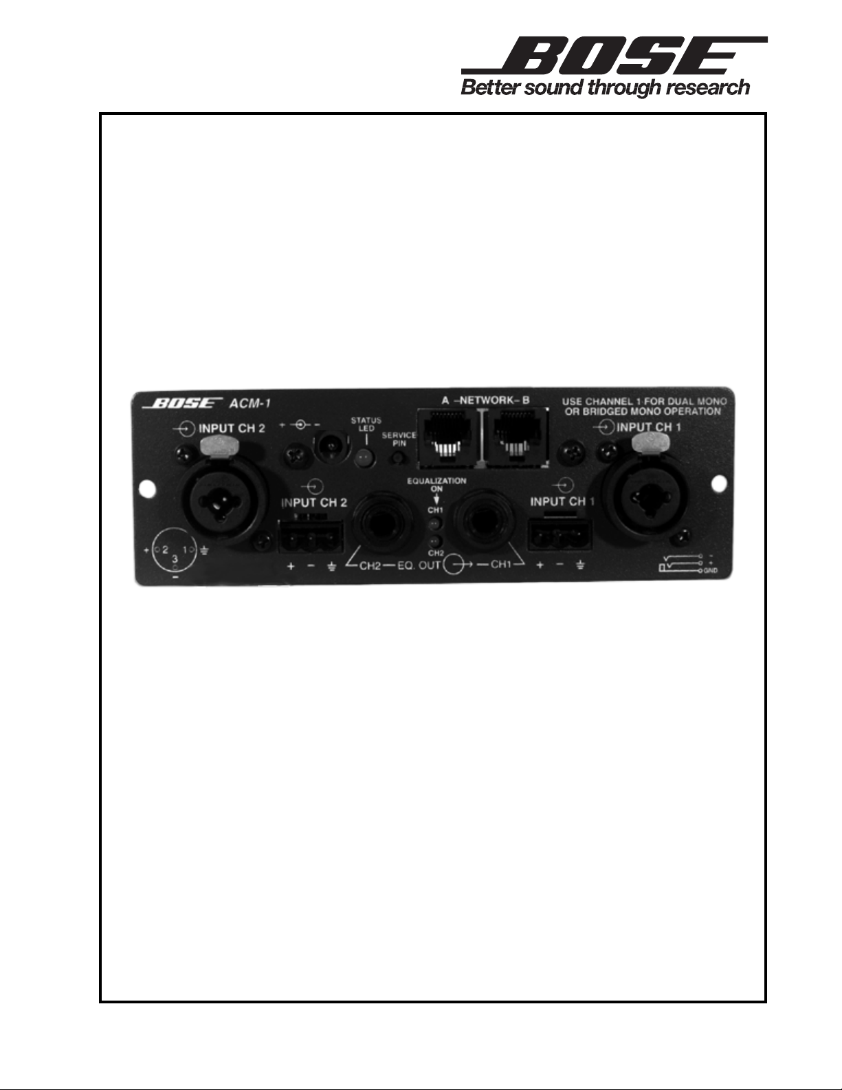
ACM-1 Amplifier Control Module
®
®
©
1999 Bose Corporation
Service Manual
Part Number 199746 Rev. 00
Page 2

CONTENTS
Safety Information............................................................................................................................ 3
Electrostatic Discharge Sensitive (ESDS) Device Handling ........................................................ 4
Warranty Information....................................................................................................................... 4
Figure 1. ACM-1 Audio Section Block Diagram................................................................................ 5
Figure 2. ACM-1 Monitoring Section Block Diagram........................................................................ 6
Theory of Operation.................................................................................................................... 7-10
Disassembly/Assembly Procedures ....................................................................................... 11-12
Figure 3. Input Module Screw Removal..........................................................................................11
Figure 4. ACM-1 Default Switch Settings....................................................................................... 11
Figure 5. 1800VI Ribbon Cable Connector Location (ACM-1 J8 to 1800VI J2) ............................ 11
Figure 6. ACM-1 J1 Ribbon Cable Connection .............................................................................. 12
Test Procedures ........................................................................................................................ 13-19
Table 1. ACM-1 Input, Output, and Power Connections................................................................. 13
Table 2. PS71 Power Supply List................................................................................................... 13
Figure 7. ACM-1 Switch Settings ................................................................................................... 14
Figure 8. 1800VI Rear Panel Switch Settings................................................................................ 14
Figure 9. ACM-1 Graphical User Interface Control Panel .............................................................. 15
Table 3. Amplifier Output Performance Tests................................................................................. 16
Test Cable Construction ............................................................................................................... 19
Part List Notes................................................................................................................................ 19
Main and Packaging Part list, ACM-1 Amplifier Control Module (see Figure 10)..................... 20
Figure 10. ACM-1 Amplifier Control Module Exploded View.......................................................... 20
Electrical part list ...................................................................................................................... 21-25
Figure 11. Daughterboard Topside Etch Layout Diagram .............................................................. 26
Figure 12. Daughterboard Internal Etch Layout Diagram .............................................................. 26
Figure 13. Daughterboard Bottom Etch Layout Diagram ............................................................... 26
Integrated Circuit Pinout Diagrams......................................................................................... 27-29
CAUTION: The ACM-1 Amplifier Control Module contains
no user serviceable parts. To prevent warranty infractions,
refer servicing to warranty service centers or factory service.
PROPRIETARY INFORMATION
THIS DOCUMENT CONTAINS PROPRIETARY INFORMATION OF
BOSE® CORPORATION WHICH IS BEING FURNISHED ONLY
FOR THE PURPOSE OF SERVICING THE IDENTIFIED BOSE
PRODUCT BY AN AUTHORIZED BOSE SERVICE CENTER OR
OWNER OF THE BOSE PRODUCT, AND SHALL NOT BE
REPRODUCED OR USED FOR ANY OTHER PURPOSE.
2
Page 3

SAFETY INFORMATION
1. Parts that have special safety characteristics are identified by the symbol on
schematics or by special notes on the parts list. Use only replacement parts that
have critical characteristics recommended by the manufacturer.
2. Make leakage current or resistance measurements to determine that exposed
parts are acceptably insulated from the supply circuit before returning the unit
to the customer. Use the following checks to perform these measurements:
A. Leakage Current Hot Check
(1) With the unit completely reassembled, plug the AC line cord directly
into a 120V AC outlet. Do not use an isolation transformer during
this test. Use a leakage current tester or a metering system that
complies with American National Standards Institute (ANSI) C101.1
"Leakage Current for Appliances" and Underwriters Laboratories
(UL) 1492 (71).
(2) With the unit AC switch first in the ON position and then in the OFF position,
measure from a known earth ground (metal water pipe, conduit, etc.) to all
exposed metal parts of the unit (antennas, handle bracket, metal cabinet,
screwheads, metallic overlays, control shafts, etc.), especially any
exposed metal parts that offer an electrical return path to the chassis.
(3) Any current measured must not exceed 0.5 milliamp.
(4) Reverse the unit power cord plug in the outlet and repeat test.
ANY MEASUREMENTS NOT WITHIN THE LIMITS SPECIFIED HEREIN
INDICATE A POTENTIAL SHOCK HAZARD THAT MUST BE ELIMINATED
BEFORE RETURNING THE UNIT TO THE CUSTOMER.
B. Insulation Resistance Test Cold Check
(1) Unplug the power supply and connect a jumper wire between the two
prongs of the plug.
(2) Turn on the power switch of the unit.
(3) Measure the resistance with an ohmmeter between the jumpered AC plug
and each exposed metallic cabinet part on the unit. When the exposed
metallic part has a return path to the chassis, the reading should be
between 1 and 5.2 Megohms. When there is no return path to the chassis,
the reading must be "infinite". If it is not within the limits specified, there is the
possibility of a shock hazard, and the unit must be repaired and rechecked
before it is returned to the customer.
3
Page 4

ELECTROSTATIC DISCHARGE SENSITIVE
(ESDS) DEVICE HANDLING
This unit contains ESDS devices. We recommend the following precautions when repairing,
replacing, or transporting ESDS devices:
• Perform work at an electrically grounded work station.
• Wear wrist straps that connect to the station or heel straps that connect to conductive floor
mats.
• Avoid touching the leads or contacts of ESDS devices or PC boards even if properly
grounded. Handle boards by the edges only.
• Transport or store ESDS devices in ESD protective bags, bins, or totes. Do not insert
unprotected devices into materials such as plastic, polystyrene foam, clear plastic bags,
bubble wrap, or plastic trays.
WARRANTY INFORMATION
• The ACM-1 Amplifier Control Module is covered by a 5-year transferable limited warranty.
4
Page 5

GND
IN1+
IN1-
IN2+
IN2-
GND
A
Circuitry
2
Unbalanced
Figure 1. ACM-1 Audio Section Block Diagram
Mode Switch
SW1A SW1B MODE
0
011 1
don't care
don't care
Truth Table
bridged
0
dual mono
normal
normal
SW2B
SW1B
Protection
3
Balanced
U16
6
A
Protection
Circuitry
HF Switch
5
2
0
U10
Selector
2
3
U15
Balanced
Unbalanced
6
1
SW1A
SW2
HF2
Eq Card 2
2
7
0
1
Selector
U12
5
2
U13
1
7
Selector
SW2A
1
Switchable
Inverter
U11
5
1
SW1B
SW2B
HF1
J6-4
Eq Card 1
J6-5
7
1
2
A
5
Buffer
Driver
U7
7
Protection
Circuitry
CH. 2 EQ
OUTPUT
5
21
U14
22
5
Buffer
Driver
U8
7
Protection
Circuitry
P2
J1-20
AMP IN 2
ENABLE I07
Attenuator
0 -100 dB
Digital
12
14
8VCLK
Clock Logic
U21
4
3
13
A
3
Buffer
Driver
U7
1
Protection
Circuitry
CH. 1 EQ
OUTPUT
P3
DATA I08
3
Buffer
Driver
U8
1
Protection
Circuitry
J1-16
AMP IN 1
5
Page 6
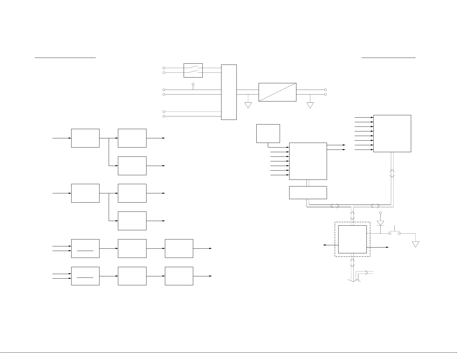
Signals from Amplifier
Therm 1
Therm 2
Rail Voltage
+I Out 1
-I Out 1
+I Out 2
-I Out 2
Protect 1
Protect 2
I Out +1
Rectification
Network Power (dc / dc)
Adapter Power (ac / dc)
Amplifier Power (dc)
Mean
Peak
V1_Mean
V1_Peak
Jumper
Standby
Wired 'OR'
D
Rectifier
Thermal
Sensor
Therm 1
Therm 2
106 dc
Standby
Protect 1
Protect 2
Regulator
A
Multiplexer
+5Vdc
Gnd.
V1_Mean
V1_Peak
V2_Mean
V2_Peak
I1_Mean
I2_Mean
Aux 1
Aux 2
Signals to Amplifier
Amp In 1
Amp In 2
Power-up
LED
Analog to Digital
Converter
10-bit Serial
6
I Out +2
I Out 1+
I Out 1-
I Out 2+
I Out 2-
Rectification
Current
Sense
Divider
Current
Sense
Divider
Mean
Peak
V2_Mean
V2_Peak
Rectification Mean
Rectification Mean
Figure 2. ACM-1 Monitoring Section Block Diagram
I1_Mean
I2_Mean
Level Shifting
Power-up
Data Bus
Neuron
Micro-
processor
Network (LonWorks®)
Service LED
Service Pin
Amplifier
Data
Activity
LED
Network Power
Gnd.
Page 7

G
eneral Description:
THEORY OF OPERATION
The Bose
®
ACM-1 Amplifier Control Module is an optional replacement for the standard
Input Module that is delivered with the Bose 1600 and 1800 Series VI Power Amplifiers.
This module, which installs into the back of the amplifier in place of the standard input
module, adds a network interface to the power amplifier; allowing the user to control and
monitor the amplifier(s) remotely and simultaneously. This can be done only when the
amplifier is in standby or 'sequence' mode, which is set on the front of the amplifier. The
network topology used by the ACM-1 Amplifier Control Module is the LonWorks
standard which is a registered trademark of Echelon
the amplifier(s) may be a personal computer or any other 'smart' device that incorporates
a LonWorks
Neuron® module.
®
Corporation. The device controlling
®
network
The Bose ACM-1 uses a LonWorks Neuron module to translate network polls into
addressing, reading and writing commands used to control the amplifier. This device
contains a network transceiver and a micro-controller interacting with on-board flashmemory. On the main PCB of the ACM-1, an Analog to Digital Converter (ADC)
translates amplifier operating conditions such as output level, temperature and clipping
level inside the amplifier to digital information to be passed to and from the Neuron module
and ultimately, the network. This information can be monitored with a computer either
locally, tied directly to the control network of the installation, or remotely, provided that the
remote computer has a network connection such as a modem (Internet), Ethernet, or LAN,
and the required software. The amplifier itself is controlled by setting a digital/analog signal
attenuator to manipulate volume level, as well as to switch the amplifier from stand-by
mode to operate mode and vice versa.
The ACM-1 is normally fed stand-by power by an external 12 Vrms AC power adapter
when the amplifier is off or in stand-by (sequence) mode. This allows the amplifier to be
turned on remotely by providing a constant power source to the Neuron module and the
Analog to Digital Converter. The amplifier cannot supply power to the Neuron module
when the amplifier is switched off, which is why the AC adapter is required. Without this
keep-alive voltage, the amplifier would not be able to be powered up remotely. Once the
amplifier is operating, the keep-alive voltage could fail and still have the amplifier operate.
Once the amplifier is shut off again, however, the keep-alive voltage must again be
present to allow remote turn-on of the amplifier. The recommended AC power adapter is
the Bose PS71. See Table 2 on page 12 for part numbers for the various models.
The keep-alive voltage input circuitry of the ACM-1 is designed to also allow the use of a
DC external stand-by power source. The nominal power requirements for a DC source
are +12 Vdc at 100 mA. Furthermore, it is also possible to power the ACM-1 via the
network cable. This must be a DC source. Although this mode of powering has its
limitations due to wire length and thickness, this option might be very useful in smaller or
highly segmented applications. To use network power, jumpers at JB1 on the daughterboard must be set. Place jumpers across pins 1 & 2 and across pins 5 & 6 at JB1. Refer
to sheet 2 of the schematic diagram at coordinates [D5]. The daughterboard is the small
board mounted to the faceplate with the RJ45 connectors on it. Refer to the daughterboard
layout diagrams on page 23. The ACM-1 is shipped with the jumpers uninstalled in order
to avoid RFI noise coupling onto the network wire, which may degrade amplifier
performance when this mode is not used.
Refer to the ACM-1 Schematic Diagram, Sheet 2 of 2, for the following information.
Note: The designators inside the brackets "[ ]" are the schematic grid coordinates which
are provided in order to make it easier to locate components on the schematic sheet
indicated in the description.
7
Page 8

THEORY OF OPERATION
Power Supply Section:
The required keep-alive voltage for the ACM-1 enters the unit at J11 [C7] as V_IN. This
input voltage is rectified, if necessary, by D32 and C44 [C7]. The DC voltage is regulated
by the +5V regulator U18 [C7]. This keep-alive power is required by the components that
allow the amplifier to be powered up remotely, the Neuron
schematic], and the Analog to Digital Converter U9 [Sheet 1, B3]. D31 and D30 [C7]
together form a wired 'OR' gate. This means that if the amplifier is powered-up, the ACM1 receives power from it, which is +15 Vdc regulated down to +5 Vdc by U18. If not, the
ACM-1 is powered from the standby power source, which could be an AC adapter, a DC
adapter, or a DC voltage supplied through the network cable. STANDBY [B4] is the
network power source which is passed through R97 [B4] to make STBYOK, which is
passed on to the ADC Multiplexer U17 [Sheet 1, C1/2], and is used to detect if there is
adapter power available, even when the amplifier is turned on. Note that digital ground is
used for the power supply reference in order to keep the analog ground after the +5V
regulator as clean as possible.
The ACM-1 consists of a power supply section, an analog section, which is the audio
signal path to the power amplifier, and a digital section which controls and monitors the
amplifier.
Note: The schematics and theory of operation of the neuron module will not be covered in
detail in this section.
®
module [not shown on
Refer to the ACM-1 Schematic Diagram, Sheet 1 of 2, for the following information.
Audio signal path:
The input stage is a balanced input receiver composed of U15 and U16 [C/D7]. The input
is taken from either the combi input connectors [D2/3] or the euro screw terminal inputs at
J4 and 5 [Sheet 2, B7]. The shield ground is decoupled from the analog ground by
capacitors C14 and C15. All inputs have spark gaps to avoid possible damage due to
static electricity. All input legs have RFI low-pass filters [C/D 7/8] and diode clamps to
protect the op-amps against overload. The input impedance in each leg is approximately
25k Ohms and is laser trimmed for good common-mode rejection.
After the input signal is converted from balanced to unbalanced, the signal enters
switchable op-amps U10 and U12 [C/D6]. These op-amps are used to route the signal
through the optional loudspeaker equalizer cards that can be installed on the ACM-1
motherboard. The presence of the EQ cards is detected automatically. If the EQ card is
plugged into its socket, the EQ1USED or EQ2USED at J6-6 or J7-6 [Sheet 2, B7] signal
is grounded causing U10 and/or U12 to route the audio signal through the EQ-cards, by
pulling the SW1A and SW2A signals at U10 or U12 low. Also, the appropriate section of
the green dual LED D50 [Sheet 2, A4] will be turned on to indicate the card is installed.
Further, the high-pass filter available on the EQ cards can be activated by setting switch
SW2 [Sheet 2, D7] to the correct position. This causes signal HF1 and HF2, which are
routed to the EQ cards via J6 and J7 [Sheet 2, B7] to be grounded.
After the signal is equalized, the audio signal is passed on to a second set of switchable
op-amps, U11 and U13 [C/D6]. The function of this op-amp pair is to set the mode of
operation of the amplifier: normal (stereo) mode, bridged mode or dual-mono mode. If
SW2B is high, the amplifier is in normal mode regardless of the state of the SW1B signal.
SW2B basically routes the signal of channel 1 into channel 2 if it is pulled low. By doing
this, the amplifier is configured in bridged mode or dual mono mode, depending on SW1B,
which inverts the signal going into channel 2, or not. When SW1B is high, the signal is not
inverted and the amplifier is in dual mono mode; if it is pulled low, the amplifier is in bridged
mode. The configuration of the mode of the amplifier is done by setting the SW1 to the
correct position [Sheet 2, D7].
8
Page 9

THEORY OF OPERATION
The equalized signal is also routed to U7 [C/D6] which forms output line drivers. The
output of the EQ card is then available to link to the next amplifier, minimizing the need for
additional EQ cards. This signal is available at the female EQ output jacks P2 and P3
[C/D4] on the frontplate of the ACM-1 module. These outputs are also equipped with RFI
low-pass T-filters, diode clamps and spark-gaps. The output impedance at audio
frequencies is approximately 400 Ohms, making it possible to drive long cable lengths
without oscillation.
After the audio signals are equalized and composed in such a way as to set the correct
mode of the amplifier, they are routed into a software controlled attenuator U14 [D5]. With
this attenuator, the level of the audio signal can be attenuated in steps of 1 dB from 0 dB
all the way down to -100 dB. The lowest attenuation level is a full mute. The attenuation
level is set by the serial data stream IO9 (DATA) from the Neuron
addressed with I07 (ENABLE) with the timing signal supplied by IO8 (CLOCK), which is
generated by the Neuron. The 3.16 k Ohms resistors R40, 41, and 42, protect U14 from
damage when the ACM-1 is in standby mode. In this mode, the attenuator is off, but the
Neuron is still powered. The quad-NAND U21 [Sheet 2, C4/5] generates VCLK from the
ENABLE and CLOCK signal. This logic is used by the TC9412F attenuator. After the
level is set with the attenuator, signal buffer U8 [C/D4] routes the signal out through J1
pins 16 and 20 [Sheet 2, B7] to the power stages of the amplifier.
Monitoring and control, digital section:
Refer to the ACM-1 Schematic Diagram, Sheet 1 of 2, for the following information.
®
. The attenuator is
The monitoring and control of the amplifier is performed by the plug-in LonWorks
module (not shown on schematic) which plugs into the ACM-1 motherboard at J9 and J10
[Sheet 2, A/B7]. This module incorporates a network transceiver which is connected to the
system's control network by means of RJ-45 connectors J12 and J13 [Sheet 2, D4],
which are located on the daughterboard.
The Neuron module switches the amplifier to operate mode by pulling low the IO6 signal
on transistor Q1 [Sheet 2, A4]. This transistor causes current to flow into the opto coupler,
located inside the amplifier which fires the TRIAC in the amplifier's power supply. Refer to
the 1600VI/1800VI service manual, Bose
the amplifiers.
Each Neuron module is assigned its own unique identification number when it is
manufactured. It can only be activated and controlled by this unique address. If the
address number for a Neuron module is lost, the unit can identify itself on the network by
toggling its service pin. This pin is connected to the momentary switch on the front-panel
of the ACM-1 module. When this switch is depressed, the SERV pin is grounded and the
yellow LED lights up. The LED is also used to indicate network activity in the ACM-1. In
this mode the LED is lit constantly. The LED blinks with a 50% duty-cycle when the
neuron module is not yet configured on the network.
The amplifier is equipped with an LED on the front of the amplifier, located in the center of
the front panel, used to indicate network activity. It is triggered by Q4 [Sheet 2, A4], which
is turned on and off via the IO5 pin from the Neuron's micro-processor.
The Neuron gets its status information via the Analog to Digital Converter U9 [B3]. This is
a serial 10-bit ADC with 8 inputs. It communicates with the Neuron on the same DATA
line. The serial timing is delivered via the IO8 CLOCK signal and the IO1 signal which
basically functions as a control signal (the control clock for successive approximation
circuitry inside the chip) for the ADC. IO0 toggles the chip select pin and the output
enable pin. When they are both low, the falling edge of the IO8 shifts out the conversion
data out of the output pin connected to IO10. IO9 shift serial data into the converter. For
detailed timing information, consult the National Semiconductor datasheet on the ADC1038.
®
part number 199747, for more information on
®
Neuron
9
Page 10

THEORY OF OPERATION
The ADC inputs are all equipped with diode clamps to protect its inputs from damage due
to a 15V input signal. This failure could occur if one of the components connected to the
ADC fails and shorts one of the 15V rails to the inputs. The resistors on the inputs of the
ADC protect the input stages of the converter against excessive currents due to fault
signals.
Six of the inputs directly sample six status signals. The other two are connected to a dual
4 channel multiplexer U17 [C1] which makes it possible to sample eight more different
status signals. V1_PEAK, V2_PEAK, V1_MEAN, V2_MEAN, I1_MEAN and I2_MEAN are
the mean and peak voltage and current levels directly measured at the output of the
power amplifier. With these signals, output signal levels can be displayed and the load
impedances can be calculated and used in the User Interface(s) connected via the
network.
The peak and mean output voltage levels are generated with U1, U2 and U3. U1 [C7]
divides down the +IOUT1 80 Vpk signal from the amplifier's output. After this, the signal
undergoes double sided rectification. From the rectified signal, the mean voltage is created
by a RC filter section, N14 [C6] and C24 [C6] and buffered with an op-amp. The
V1_MEAN output is taken from U1 pin 14 [C6]. In another op-amp stage, U3 [C5], the
peak signal is derived with a peak-hold circuit. The peak level is stored in C28 [B5].
V1_PEAK is taken off of U3 at Pin 7 [C5]. +IOUT2 is processed in the same way using
U2 and U3.
The mean current level is generated with U4 and U5 [A5-7]. Because the output current is
measured across the 20 milliOhm resistor that is installed inside the amplifier, the signal
needs to be divided down before it is routed into the balanced input stage formed by U4
and U5. The division is done by the 5 kOhms resistor arrays N16-19 [A/B7]. After
converting the signal into an unbalanced signal, the signal is double sided rectified. RC
filters R5/C26 [A5] and R6/C27 [A5] filter the signal and produce the scaled mean of the
output current for both amplifiers. U4 and U5 buffer this signal before it is routed into the
ADC [B3].
The dual multiplexer U17 together with U6 [C1] produce two extra buffered signals which
are routed into the remaining two inputs of the ADC. With the multiplexer, the Neuron
select which parameter should be sampled. These parameters are connected to the 8
inputs of the mutiplexer and can be selected with IO2A and IO3A. These 2 signals are
level shifted to +15V and inverted with transistors Q2 and Q3 [Sheet 2, A5]. Two inputs
are selected at the same time and fed to the ADC. XTEMP is the temperature on the ACM1 motherboard and is generated with temperature sensor U20 [C2]. 316ADD1 and
316ADD2 are generated by the amplifier and indicate that the relays at the outputs of the
amplifier are open due to a short circuit condition or due to DC offset caused by amplifier
failure. These signals are also supplied to the User Interface(s) to indicate that impedance
measurement is then invalid due to the opened relays.
The 106VDC (1800VI), 90VDC (1600VI) signal indicates the presence of the power
amplifier rail voltage. It is a divided down version of the rail voltage, and is used by the
User Interface(s) to detect proper operation of the amplifier.
THERM1 and THERM2 are voltages generated by the temperature sensors on the power
amplifier stage's heatsinks. With these scaled voltages the temperature of these stages
can be measured and displayed on the User Interface.
STDBYOK is the voltage derived from the standby power from the mains adapter or the
network. It is used to indicate if the amplifier can be turned back on after it is powered
down.
®
can
10
Page 11

DISASSEMBLY/ASSEMBLY PROCEDURES
Note: In order to test the ACM-1 Amplifier
Control Module, you must first remove the
standard input module that is supplied by
the factory from the rear of the amplifier.
1. Input Module Removal
1.1 Use a phillips-head screwdriver to
remove the two screws from the input
module connector panel. The input module
is located on the rear of the amplifier.
See Figure 3.
1.2 Pull the input module partially out of
the chassis.
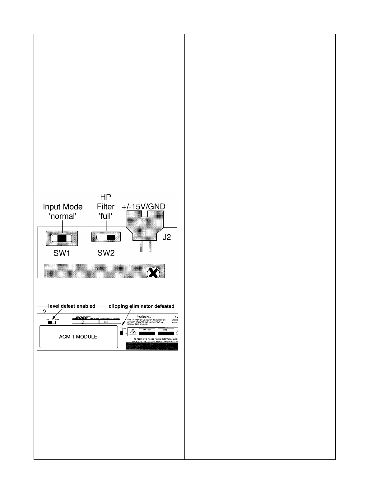
Figure 4. ACM-1 Default Switch Settings
1.3 Disconnect the amplifier ribbon cable
from the input module J1 connector.
Figure 3. Input Module Screw Removal
Note: Before installing the ACM-1 module
into the amplifier, you must set the switches
on the ACM-1 to the default settings.
Note: DO NOT install any EQ cards into
the ACM-1 module that may have been
installed in the standard input module.
Installing these cards will change the
response of the ACM-1 and make the tests
invalid.
2. ACM-1 Module Installation
2.1 Connect the ribbon cable from the
J8 connector of the ACM-1 to the J2
connector located on the I/O board of the
amplifier. This connector is fairly difficult to
insert. Pin 1 (red stripe) of the ribbon cable
is to the right. See Figure 5.
Default switch settings:
On the ACM-1 Module, place the Input
Mode Switch SW1 to the NORMAL (center)
position. Place the HF/Full Range Switch
SW2 to the FULL (right) position.
See Figure 4.
Figure 5. Amplifier Ribbon Cable Connector
Location (ACM-1 J8 to amplifier J2)
11
Page 12

DISASSEMBLY/ASSEMBLY PROCEDURES
2.2 Connect the amplifier's ribbon cable to
the ACM-1 module J1 connector. Pin 1 (red
stripe) of the ribbon cable is to the right.
See Figure 6.
Figure 6. ACM-1 J1 Ribbon
Cable Connection
3.4 Disconnect the ACM-1's ribbon cable
from the amplifier's J2 connector.
4. Input Module Replacement
4.1 Connect the amplifier's ribbon cable
to the input module connector at J1.
Pin 1 (red stripe) of the ribbon cable is
to the right.
4.2 Slide the input module into the
chassis slot until the input module J2
connector is completely seated into the
amplifier's two-pin harness connector.
The input module should be flush with
the chassis back panel.
4.3 Secure the input module to the
amplifier chassis with the two screws
using a phillips-head screwdriver.
2.3 Slide the ACM-1 module into the
chassis slot until the module's J2 connector
is completely seated into the amplifier twopin harness connector. The module should
be flush with the chassis back panel.
2.4 Secure the ACM-1 module to the
amplifier chassis with two screws using a
phillips-head screwdriver.
Note: The ACM-1 Module will not operate
properly unless at least one screw is used
to secure it to the amplifier. The faceplate
of the ACM-1 is used to provide a ground
connection to the amplifier.
3. ACM-1 Module Removal
3.1 Use a phillips-head screwdriver to
remove the two screws from the ACM-1
module connector panel.
3.2 Pull the input module partially out of
the chassis.
3.3 Disconnect the amplifier's ribbon cable
from the input module's J1 connector.
12
Page 13

TEST PROCEDURES
Function PCB Location Type of Connection
Source Input Ch. 1 P4 Balanced TRS; tie LO to ring, tie HI to tip,
tie ground to sleeve.
Source Input Ch. 2 P1 Balanced TRS; tie LO to ring, tie HI to tip,
tie ground to sleeve.
Source Input Ch. 1 (Euro) J4 Three position connector; tie LO to -, tie HI
to +, tie ground to GND.
Source Input Ch. 2 (Euro) J5 Three position connector; tie LO to -, tie HI
to +, tie ground to GND.
External Power Supply (PS71) J11 Co-axial; connect LO (gnd) to sleeve,
connect HI (12VAC) to tip.
LonWorks® Network Connector
(for monitoring and control)
EQ Output Ch. 1 P3 Balanced TRS; tie LO to ring, tie HI to tip,
EQ Output Ch. 2 P2 Balanced TRS; tie LO to ring, tie HI to tip,
J12 or J13 RJ45; use standard CAT-5 network cable
with crimped RJ45 connectors.
tie ground to sleeve.
tie ground to sleeve.
Table 1. ACM-1 Input, Output, and Power Connections
Test Setup Parameters
1. In order to be able to perform these
tests, you will need the following:
• A Microsoft® Windows® compatible
computer with at least 40Mbytes of hard
disk space, 32Mbytes of RAM and a CD
ROM drive.
• Bose® Entero™ software (CD ROM)
• Windows 95 or Windows NT 4.0.
• Network Interface Card, such as the
Echelon PCNSI for desktops or the
PCC-10 for laptops.
• The Echelon LNS (LonWorks® Network
Services) software must be installed on
the computer you are using for testing.
This enables management of the
LonWorks database and direct
communication with nodes on the
network.
• Bose 1600VI or 1800VI power amplifier.
• Bose PS71 external power supply as
listed in Table 2 below.
Power Supply Bose Part Number
UL 120 VAC 178371
230V Euro 178375
230V UK/Singapore 178374
240V Australia 178373
100V Japan 178372
Table 2. PS71 Power Supply List
13
Page 14
TEST PROCEDURES
Test Setup Parameters (continued)
2. Default switch settings: On the ACM-1
Module, place the Input Mode Switch SW1
to the NORMAL (center) position.
Place the HF/Full Range Switch SW2 to the
FULL (right) position. See Figure 7.
On the amplifier rear panel, place the Level
Defeat Switch to the ENABLED (on) position. This disables the volume controls on
the amplifier front panel.
Place the Clipping Eliminator Switch to the
DISABLED (off) position, and the Power
Switch to the STANDBY position. See
Figure 8.
3. Install the ACM-1 Module into the rear
of the amplifier using Disassembly/
Assembly procedures 1 & 2.
4. Connect the PS71 external power
supply to an AC Mains connection and to
the Standby Power connector at J11 on the
ACM-1 Module. This will provide power to
allow the module to be controlled by the
network before the amplifier is powered up.
5. Connect the CAT-5 network cable
between the network interface card located
in the computer and the ACM-1 module.
6. Four signal paths are used during
testing. They are as follows:
• Source Input Ch.1 to EQ output Ch.1.
• Source Input Ch.2 to EQ output Ch.2.
• Source Input Ch.1 to amp output Ch.1.
• Source Input Ch.2 to amp output Ch.2.
Figure 7. ACM-1 Switch Settings
Figure 8. Amplifier Rear Panel Switch
Settings
Note: If the Power Switch on the front
panel of the amplifier is not in the
STANDBY position, you will not be able to
control the amplifier using the network.
7. For each signal path there are two basic
input/output terminations to be used.
• Noise Test Termination - Noise is
measured in a bandwidth of 20 Hz to 22
kHz with no weighting function. The
source inputs (+ and -) are not to be
driven with signal, but terminated with 50
Ohms. Power amplifier outputs are
measured across an 8 Ohm, 500 Watt
load connected across the outputs.
The EQ outputs of the ACM-1 are
measured across a 10 kOhm load
terminating the unbalanced outputs
(each leg to ground).
• Gain, Response and Distortion Test
Termination - The inputs are to be driven
from a 50 Ohm source. EQ outputs are
measured across a 10 kOhm load
terminating the unbalanced outputs.
Power amplifier outputs are measured
across an 8 Ohm, 500 Watt load
connected across the outputs.
Note: If there are any EQ PCBs installed in
the ACM-1 at J6 or J7, be sure to remove
them before testing.
14
Page 15

TEST PROCEDURES
Adding a Bose® 1600VI or 1800VI
amplifier to a network using the
Entero™ software.
1. Install the ACM-1 Amplifier Control
Module into the amplifier using
Disassembly/Assembly procedures 1 & 2.
2. Connect the network cable to J12 or J14
of the ACM-1.
3. Plug the PS71 standby power supply into
J11 of the ACM-1. Connect the power cord
of the PS71 to the AC mains.
4. Make all required audio input and output
connections.
5. Open the Entero software on the
computer screen.
6. Click on the Device Finder tab. You
should see all of the previously configured
devices (if any) on the left-hand side of the
screen.
7. Pull down the Tools menu, scroll down to
Add Device, and click the mouse. A dialog
box will open with folders listing different
types of devices.
8. Double-click on the Amplifiers folder.
9. There will be four files listed to choose
from. They are: Bose 1600 Bridge.dev;
Bose 1600 Stereo.dev; Bose 1800
Bridge.dev; and Bose 1800 Stereo.dev.
Click on the Bose 1600 Stereo.dev or the
Bose 1800 Stereo.dev file, according to
which amplifier you are using for testing.
Click on Open. The device will appear
grayed-out on the left-hand side of the
screen.
Electrical Tests
Note: Refer to Figure 9 for the following
tests.
Figure 9. ACM-1 Graphical User Interface
Control Panel
1. Network Power Up Test
1.1 Open the Entero software by double-
clicking on the icon. When the program
opens enter the password, if required, and
click OK. Click on the Device Finder tab.
The amplifier to be used for the test should
be listed in the column on the left. If the
amplifier is not listed, refer to the Appendix
in the back of this manual for information
on how to add and configure it.
1.2 Click on the icon for the amplifier, the
controls for the amplifier should appear in
the box on the right.
10. Pull down the Tools menu, scroll down
to Attach, and click the mouse. You will be
prompted to press the service pin switch on
the panel of the ACM-1. Press the service
pin switch. The device will be added to the
database and will no longer be grayed-out.
1.3 In the box to the right, you will see
several controls for the amplifier. At the
bottom left, you will see the Power button.
Click on the Power button using the mouse.
The amplifier should power up.
15
Page 16

TEST PROCEDURES
1.4 Verify that the amplifier powers up, and
that on the computer screen, the green
status light located in the controls section
next to the gain sliders lights green to
indicate proper operation of the amplifier.
2. EQ Audio Output Gain Test
2.1 Open the Entero™ software on the
computer, and select the device finder tab.
Click on the icon for the amplifier in the
left-hand column. On the right-hand side of
the screen, click on the Power button using
the mouse. The amplifier should power up.
Set the gain slider for the channel under
test to -100.0 dB.
2.2 Apply a 1 Vrms, 1 kHz signal to the
Channel 1 input of the ACM-1.
2.3 Measure the ouput level at the
Channel 1 ACM-1 EQ output at P3.
It should be 0 dBV ± 1 dB.
4. EQ Audio Output Noise Test
4.1 Open the Entero software on the
computer, and select the device finder tab.
Click on the icon for the amplifier in the
left-hand column. On the right-hand side of
the screen, click on the Power button using
the mouse. The amplifier should power up.
Set the gain slider for the channel under
test to -100.0 dB.
4.2 Terminate the ACM-1 Channel 1 audio
input at P4 (or J4) with 50 Ohms. Measure
the ACM-1 Channel 1 output at P3 across
10k Ohms, terminating each unbalanced
output leg to ground.
4.3 Measure the noise level at P3 within a
bandwidth of 20 Hz - 22 kHz with no
weighting function. It should be
-95 dBV ≤ -90 dBV.
4.4 Repeat this procedure for Channel 2.
2.4 Repeat this procedure for Channel 2.
3. EQ Audio Output THD Test
3.1 Open the Entero software on the
computer, and select the device finder tab.
Click on the icon for the amplifier in the
left-hand column. On the right-hand side of
the screen, click on the Power button using
the mouse. The amplifier should power up.
Set the gain slider for the channel under
test to -100.0 dB.
3.2 Apply a 1 Vrms, 1 kHz signal to the
Channel 1 input of the ACM-1.
3.3 Measure the THD level at the
Channel 1 ACM-1 EQ output at P3.
It should be 0.05% ± 0.1%.
3.4 Repeat this procedure for Channel 2.
5. Amplifier Output Gain Test
5.1 Open the Entero software on the
computer, and select the device finder tab.
Click on the icon for the amplifier in the
left-hand column. On the right-hand side of
the screen, click on the Power button using
the mouse. The amplifier should power up.
Set the gain slider for the channel under
test to 0.0 dB.
5.2 Apply a 775 mVrms, 1 kHz signal to
the ACM-1 Channel 1 input at P4 (or J4).
5.3 Reference a dB meter to the output.
5.4 Measure the output level at the
amplifier channel 1 output. For the 1600VI
amplifier, it should be +27.6 dBr ± 1.0 dB
for low sensitivity units and +33.3 dBr ±
1.0 dB for high sensitivity units. For the
1800VI amplifier, it should be +30.3 dBr ±
1.0 dB for low sensitivity units and 36.0 dBr
± 1.0 dB for high sensitivity units.
16
5.5 Repeat this procedure for Channel 2.
Page 17

TEST PROCEDURES
6. Amplifier Output Relative Gain Tests
6.1 Open the Entero™ software on the
computer, and select the device finder tab.
Click on the icon for the amplifier in the
left-hand column. On the right-hand side of
the screen, click on the Power button using
the mouse. The amplifier should power up.
Set the gain slider for the channel under
test to 0.0 dB.
6.2 Apply a 100 mV, 1 kHz signal to the
ACM-1 Channel 1 input at P4 (or J4).
6.3 Reference a dB meter to the amplifier
channel 1 output. This is the reference
level.
6.4 Perform the tests in Table 3 below.
Test Name Freq. Output
Gain 20 Hz 20 Hz 0 dBr ± 1.0 dBr
Reference 1 kHz 0 dBr ± 1.0 dBr
Gain 100 Hz 100 Hz 0 dBr ± 1.0 dBr
Gain 500 Hz 500 Hz 0 dBr ± 1.0 dBr
Gain 5 kHz 5 kHz 0 dBr ± 1.0 dBr
Gain 20 kHz 20 kHz 0 dBr ± 1.0 dBr
Table 3. Amplifier Output Performance Tests
6.5 Repeat this procedure for Channel 2.
7. Amplifier Output THD Test
8. Amplifier Output Noise Test
8.1 Open the Entero software on the
computer, and select the device finder tab.
Click on the icon for the amplifier in the
left-hand column. On the right-hand side of
the screen, click on the Power button using
the mouse. The amplifier should power up.
Set the gain slider for the channel under
test to 0.0 dB.
8.2 Terminate the ACM-1 Channel 1 audio
input at P4 (or J4) with 50 Ohms. Measure
the ACM-1 Channel 1 output at P3 across
10k Ohms, terminating each unbalanced
output leg to ground.
8.3 Measure the noise level at the
amplifier channel 1 output within a bandwidth of 20 Hz - 22 kHz with no weighting
function. It should be -60 dBV ≤ -55 dBV.
8.4 Repeat this procedure for Channel 2.
9. Voltage Controlled Amplifier Tests
9.1 On the Entero Graphical User
Interface Control Panel, set the sliders to
-40.0 dB. You can do this by sliding the
sliders or by clicking on the box above the
slider. A dialog box will open that will allow
you to type in the level you want.
7.1 Open the Entero software on the
computer, and select the device finder tab.
Click on the icon for the amplifier in the
left-hand column. On the right-hand side of
the screen, click on the Power button using
the mouse. The amplifier should power up.
Set the gain slider for the channel under
test to 0.0 dB.
7.2 Apply a 500 mV, 1 kHz signal to the
ACM-1 Channel 1 input at P4 (or J4).
7.3 Measure the THD level at the amplifier
channel 1 output. It should be
0.05% ≤ 0.2%.
7.5 Repeat this procedure for Channel 2.
9.2 Apply a 775 mVrms, 1 kHz signal to the
Channel 1 input of the ACM-1 module.
9.3 Measure the output at the Channel 1
output of the amplifier. For the 1600VI
amplifier it should be -14.25 dBV ± 1.0 dB.
For the 1800VI amplifier it should be
-6.4 dBV ± 1.0 dB.
9.4 Repeat this procedure for Channel 2.
17
Page 18

TEST PROCEDURES
10. Monitoring Functions Test
10.1 Open the Entero™ software on the
computer, and select the device finder tab.
Click on the icon for the amplifier in the
left-hand column. On the right-hand side of
the screen, click on the Power button using
the mouse. The amplifier should power up.
Set the gain slider for the channel under
test to 0.0 dB.
10.2 Apply a 200 mVrms, 1 kHz signal to
the ACM-1 channel 1 and 2 inputs at P4
and P1. Verify that the GUI Display for Z1
and Z2 reads 8 Ohms ± 1 Ohm.
10.3 While the 200 mVrms, 1 kHz signal
is applied, check the GUI display at for
Temp1 and Temp2. They should read
between 20° C and 60° C, or 68° F and
140° F, depending on how long the
amplifier has been operating and what
the ambient temperature of the test
environment is.
12. Dual Mono Test
12.1 Place the Amplifier Mode Switch SW1
on the ACM-1 to the DUAL MONO position
(full right).
12.2 Open the Entero software on the
computer, and select the device finder tab.
Click on the icon for the amplifier in the
left-hand column. On the right-hand side of
the screen, click on the Power button using
the mouse. The amplifier should power up.
Set the gain slider for the channel under
test to 0.0 dB.
12.3 Apply a 100 mVrms, 1 kHz signal to
the ACM-1 Channel 2 input only.
12.4 Measure the output level at the
Channel 1 output of the amplifier. For the
1600VI amplifier it should be 7.35 dBV ±
1.0 dB. For the 1800VI amplifier it should
be 15.6 dBV ± 1.0 dB.
11. Bridged Mono Test
11.1 Place the Amplifier Mode Switch SW1
on the ACM-1 to the BRIDGED position
(full left).
11.2 Open the Entero software on the
computer, and select the device finder tab.
Click on the icon for the amplifier in the
left-hand column. On the right-hand side of
the screen, click on the Power button using
the mouse. The amplifier should power up.
Set the gain slider for the channel under
test to 0.0 dB.
11.3 Apply a 100 mVrms, 1 kHz signal to
the ACM-1 Channel 2 input only.
11.4 Measure the output level at the
Channel 1 output of the amplifier. For the
1600VI amplifier it should be 7.35 dBV ±
1.0 dB. For the 1800VI amplifier it should
be 15.6 dBV ± 1.0 dB.
18
Page 19

TEST PROCEDURES
Test Cable Construction
If you need to troubleshoot an ACM-1
outside of the amplifier chassis, you will
need to make a test cable.
You can do this by unsoldering the 4-pin
Molex connector at J2 from the rear of the
ACM-1 board and soldering a twisted-pair
of wires on to pins 1 and 2. These are the
terminals that are the closest to the connector and correspond to the bottom pins
of the connector itself. It's recommended
to use two different color wires to avoid
errors. Refer to the component layout
diagram for location.
Solder the other ends of the wires to the
corresponding pads on the board.
The +15Vdc terminal at J2 pin 2 is tied to
D40 and C92. The -15Vdc terminal at J2
pin 1 is tied to D41 and C93. Be sure to
solder the wires to the correct terminals or
you will destroy the PCB.
This cable will allow you to plug the into
the Molex connector in the card slot of the
1600/1800VI amplifier and operate the
ACM-1 outside of the amplifier chassis.
Note: Be sure to connect a ground wire
from the front panel of the ACM-1 to the
chassis of the amplifier. The ACM-1 will
not operate without this ground wire.
PART LIST NOTES
1. This part is not normally available from Customer Service. Approval from the Field Service
Manager is required before ordering.
2. The individual parts located on the PCBs are listed in the Electrical Part List.
3. This part is critical for safety purposes. Failure to use a substitute replacement with
the same safety characteristics as the recommended replacement part might create shock,
fire, and/or other hazards.
19
Page 20

MAIN AND PACKAGING PART LIST
ACM-1 Amplifier Control Module (see Figure 10)
Item
Description Part Number Qty.
Number
1 SCREW, MACH, 6-32X.25, PAN, XREC 107343-04 4
2 MODULE, NEURON, TPFT-10F,
193966-01 1
ECHELON P/N: 55020-10
3 CHIP, FLASH, EXTENSOR 193965-01 1
4 PCB ASSY, DAUGHTERBOARD 196387 1
5 PANEL, FRONT 188663 1
6 SCREW, MACH, M3X0.5X5.0, PAN, XREC 183435-05 4
7 PCB ASSY, MOTHERBOARD 196343 1
8 SPACER, HEX, STEEL, 6-32X.5 196392-08 2
9 MANUAL, OWNER'S GUIDE 193962 1
10 CARTON, RSC VENDOR
SUPPLIED
4X
1
3
2
4
5
6
1
7
2X
8
1
6
9
10
Figure 10. ACM-1 Amplifier Control Module Exploded View
20
Page 21

ELECTRICAL PART LIST
Resistors
Reference
Designator
R1 100K, 0805, 1/10W, 1% 133625-1003
R2 100K, 0805, 1/10W, 1% 133625-1003
R3 100K, 0805, 1/10W, 1% 133625-1003
R4 100K, 0805, 1/10W, 1% 133625-1003
R5 100K, 0805, 1/10W, 1% 133625-1003
R6 100K, 0805, 1/10W, 1% 133625-1003
R43 100K, 0805, 1/10W, 1% 133625-1003
R44 100K, 0805, 1/10W, 1% 133625-1003
R40 3.16K, 0805, 1/10W, 1% 133625-3161
R41 3.16K, 0805, 1/10W, 1% 133625-3161
R42 3.16K, 0805, 1/10W, 1% 133625-3161
R45 JUMPER CHIP, 0805 133627
R47 JUMPER CHIP, 0805 133627
R60 392K, 0805, 1/10W, 1% 133625-3923
R61 392K, 0805, 1/10W, 1% 133625-3923
R62 392K, 0805, 1/10W, 1% 133625-3923
R63 392K, 0805, 1/10W, 1% 133625-3923
R70 12.1Ω, 0805, 1/10W, 1% 133625-12R1
R76 330K, 0805, 1/10W, 5% 133626-3345
R77 330K, 0805, 1/10W, 5% 133626-3345
R78 330K, 0805, 1/10W, 5% 133626-3345
R79 330K, 0805, 1/10W, 5% 133626-3345
R80 1.0K, 0805, MF, 1% 181896-1001
R81 1.0K, 0805, MF, 1% 181896-1001
R82 1.0K, 0805, MF, 1% 181896-1001
R83 1.0K, 0805, MF, 1% 181896-1001
R98 1.0K, 0805, MF, 1% 181896-1001
R90 4.99K, 0805, 1/10W, 1% 133625-4991
R91 4.99K, 0805, 1/10W, 1% 133625-4991
R92 100K, 0805, 1/10W, 1% 133625-1003
R93 100K, 0805, 1/10W, 1% 133625-1003
R94 4.22K, 0805, 1/10W, 1% 173767-4221
R95 4.22K, 0805, 1/10W, 1% 173767-4221
R97 5.10K, 0805, 1/10W, 1% 133626-5125
R96 332Ω, 0805, 1/10W, 1% 173767-332R
R99 330K, 0805, 1/10W, 5% 133626-3345
R101 330K, 0805, 1/10W, 5% 133626-3345
R100 33.2K, 0805, 1/10W, 1% 173767-3322
R102 33.2K, 0805, 1/10W, 1% 173767-3322
N1 10K, RES NET, 1/10W, 2%, X4 196347-1002
N2 10K, RES NET, 1/10W, 2%, X4 196347-1002
N3 10K, RES NET, 1/10W, 2%, X4 196347-1002
N4 10K, RES NET, 1/10W, 2%, X4 196347-1002
N5 2.7K, RES NET, 1/10W, 2%, X4 196347-2701
N24 2.7K, RES NET, 1/10W, 2%, X4 196347-2701
N6 10K, RES NET, 1/10W, 2%, X3 196346-1002
N9 10K, RES NET, 1/10W, 2%, X3 196346-1002
N7 20K, RES NET, 1/10W, 2%, X5 196345-2002
N8 20K, RES NET, 1/10W, 2%, X5 196345-2002
N10 200Ω, RES NET, 1/10W, 2%, X4 196347-2000
N11 200Ω, RES NET, 1/10W, 2%, X4 196347-2000
N12 47K, RES NET, 1/10W, 2%, X4 196347-4702
Description Part Number Note
21
Page 22

ELECTRICAL PART LIST
Resistors
Reference
Designator
N13 47K, RES NET, 1/10W, 2%, X4 196347-4702
N14 100K, RES NET, 1/10W, 2%, X4 196347-1003
N15 100K, RES NET, 1/10W, 2%, X4 196347-1003
N16 5.00K, RES NET, 1/10W, 0.1%, X8 181482-5001
N17 5.00K, RES NET, 1/10W, 0.1%, X8 181482-5001
N18 5.00K, RES NET, 1/10W, 0.1%, X8 181482-5001
N19 5.00K, RES NET, 1/10W, 0.1%, X8 181482-5001
N20 470Ω, RES NET, 1/10W, 2%, X4 196347-4700
N21 470Ω, RES NET, 1/10W, 2%, X4 196347-4700
N22 470Ω, RES NET, 1/10W, 2%, X4 196347-4700
N23 470Ω, RES NET, 1/10W, 2%, X4 196347-4700
Reference
Designator
C 2 1000pF, 0805, COG, 50V, 5% 133622-102
C 3 16pF, 0805, COG, 50V, 5% 133622-160
C 4 16pF, 0805, COG, 50V, 5% 133622-160
C 5 330pF, 0805, COG, 50V, 5% 133622-331
C 6 330pF, 0805, COG, 50V, 5% 133622-331
C 7 330pF, 0805, COG, 50V, 5% 133622-331
C 8 330pF, 0805, COG, 50V, 5% 133622-331
C1 0 5600pf, 1206, COG, 50V, 5% 177214-562
C1 1 5600pf, 1206, COG, 50V, 5% 177214-562
C14 .01uF, 0805, X7R, 50V, 10% 133623-103
C15 .01uF, 0805, X7R, 50V, 10% 133623-103
C16 .01uF, 0805, X7R, 50V, 10% 133623-103
C22 1uF, 1206, Y5V, 16V, 80% 173383-105
C23 1uF, 1206, Y5V, 16V, 80% 173383-105
C24 1uF, 1206, Y5V, 16V, 80% 173383-105
C25 1uF, 1206, Y5V, 16V, 80% 173383-105
C26 1uF, 1206, Y5V, 16V, 80% 173383-105
C27 1uF, 1206, Y5V, 16V, 80% 173383-105
C28 1uF, 1206, Y5V, 16V, 80% 173383-105
C29 1uF, 1206, Y5V, 16V, 80% 173383-105
C3 0 47 pF, 0805, COG, 50V, 5% 133622-470
C3 1 47 pF, 0805, COG, 50V, 5% 133622-470
C32 2.2 uF, EL, 85, 50V, 20% 149947-2R2H
C33 2.2 uF, EL, 85, 50V, 20% 149947-2R2H
C34 2.2 uF, EL, 85, 50V, 20% 149947-2R2H
C35 2.2 uF, EL, 85, 50V, 20% 149947-2R2H
C36 2.2 uF, EL, 85, 50V, 20% 149947-2R2H
C37 2.2 uF, EL, 85, 50V, 20% 149947-2R2H
C42 1.0 uF, EL, 85, 50V, 20% 149948-1R0H
C43 .10uF, 0805, Y5V, 25V, 80% 133624
C45 .10uF, 0805, Y5V, 25V, 80% 133624
C47 .10uF, 0805, Y5V, 25V, 80% 133624
C49 .10uF, 0805, Y5V, 25V, 80% 133624
C50 .10uF, 0805, Y5V, 25V, 80% 133624
C51 .10uF, 0805, Y5V, 25V, 80% 133624
C52 .10uF, 0805, Y5V, 25V, 80% 133624
Description Part Number Note
Capacitors
Description Part Number Note
22
Page 23

ELECTRICAL PART LIST
Capacitors
Reference
Designator
C54 .10uF, 0805, Y5V, 25V, 80% 133624
C55 .10uF, 0805, Y5V, 25V, 80% 133624
C56 .10uF, 0805, Y5V, 25V, 80% 133624
C57 .10uF, 0805, Y5V, 25V, 80% 133624
C58 .10uF, 0805, Y5V, 25V, 80% 133624
C59 .10uF, 0805, Y5V, 25V, 80% 133624
C60 .10uF, 0805, Y5V, 25V, 80% 133624
C61 .10uF, 0805, Y5V, 25V, 80% 133624
C62 .10uF, 0805, Y5V, 25V, 80% 133624
C63 .10uF, 0805, Y5V, 25V, 80% 133624
C65 .10uF, 0805, Y5V, 25V, 80% 133624
C66 .10uF, 0805, Y5V, 25V, 80% 133624
C67 .10uF, 0805, Y5V, 25V, 80% 133624
C71 .10uF, 0805, Y5V, 25V, 80% 133624
C44 330 uF, EL, 85, 25V, 20% 149948-331E
C92 100 uF, EL, 105, 50V, 20% 144000-101H
C93 100 uF, EL, 105, 50V, 20% 144000-101H
Reference
Designator
D1 DUAL, SOT-23, BAV 99R-R 147239
D2 DUAL, SOT-23, BAV 99R-R 147239
D3 DUAL, SOT-23, BAV 99R-R 147239
D4 DUAL, SOT-23, BAV 99R-R 147239
D5 DUAL, SOT-23, BAV 99R-R 147239
D6 DUAL, SOT-23, BAV 99R-R 147239
D7 DUAL, SOT-23, BAV 99R-R 147239
D8 DUAL, SOT-23, BAV 99R-R 147239
D9 DUAL, SOT-23, BAV 99R-R 147239
D10 DUAL, SOT-23, BAV 99R-R 147239
D11 DUAL, SOT-23, BAV 99R-R 147239
D12 DUAL, SOT-23, BAV 99R-R 147239
D13 DUAL, SOT-23, BAV 99R-R 147239
D14 DUAL, SOT-23, BAV 99R-R 147239
D15 DUAL, SOT-23, BAV 99R-R 147239
D16 DUAL, SOT-23, BAV 99R-R 147239
D17 DUAL, SOT-23, BAV 99R-R 147239
D18 DUAL, SOT-23, BAV 99R-R 147239
D19 DUAL, SOT-23, BAV 99R-R 147239
D20 DUAL, SOT-23, BAV 99R-R 147239
D30 AXIAL, 500V, 35A, 1N4004 146515-4
D31 AXIAL, 500V, 35A, 1N4004 146515-4
D32 AXIAL, 500V, 35A, 1N4004 146515-4
D40 ZENER, 18V, 1W, 5%, 1N4746 116995-4746A
D41 ZENER, 18V, 1W, 5%, 1N4746 116995-4746A
D42 ZENER, .5W, 12V 174265-5242
D43 ZENER, .5W, 12V 174265-5242
D50 DIODE, LED, DUAL GREEN 196355
D51 DIODE, LED, LUMEX, SINGLE 196356
Description Part Number Note
Diodes
Description Part Number Note
23
Page 24

ELECTRICAL PART LIST
Transistors
Reference
Designator
Q1 BPLR, P, 40V, 200mA, SOT23 148596
Q2 BPLR, N, 40V, 200mA, SOT23 146819
Q3 BPLR, N, 40V, 200mA, SOT23 146819
Q4 BPLR, N, 40V, 200mA, SOT23 146819
Reference
Designator
U1 OP-AMP, QUAD, SOIC-14, NJM2059 187472
U2 OP-AMP, QUAD, SOIC-14, NJM2059 187472
U3 OP-AMP, QUAD, SOIC-14, NJM2059 187472
U4 OP-AMP, QUAD, SOIC-14, NJM2059 187472
U5 OP-AMP, QUAD, SOIC-14, NJM2059 187472
U6 OP-AMP, DUAL, SOIC-8, NJM4559 187473
U7 OP-AMP, DUAL, SOIC-8, NJM4559 187473
U8 OP-AMP, DUAL, SOIC-8, NJM4559 187473
U9 ADC, 10 BIT / 8 IN, ADC1038, SO20 196360
U10 OP-AMP SWITCH, SOIC-8, NJM2120 187474
U11 OP-AMP SWITCH, SOIC-8, NJM2120 187474
U12 OP-AMP SWITCH, SOIC-8, NJM2120 187474
U13 OP-AMP SWITCH, SOIC-8, NJM2120 187474
U14 VOL CTL, ST, TC9412AF 196350
U15 OP-AMP, SSM2141S, SOIC-8 196348
U16 OP-AMP, SSM2141S, SOIC-8 196348
U17 MUX, 2X4IN/1OUT, CD4052BCM, SO16 196351
U18 REG, ISOPKG, +5V, L7805CP, TO220 196361
U20 TEMP SENSOR, LM50C1M3, SOT23 196352
U21 NAND, DUAL 2 IN NAND, SMD, MM74HC00M 186065
Description Part Number Note
Integrated Circuits
Description Part Number Note
24
Page 25

ELECTRICAL PART LIST
Miscellaneous
Reference
Designator
J1 CONN, 10X2 ROWS, .1 GRID, MALE 196364
J2 CONN, MOLEX, PCB MT,
4 PIN
J3A CONN, HEADER, W/ SPACER, 8 PIN 196359
J3 B CONN, HEADER, BTM INSERT, 4x2 PIN GRID 196358
J4 CONN, RTANG, 3 POS, BLK 177291-03
J5 CONN, RTANG, 3 POS, BLK 177291-03
J6 CONN, TOP ENTRY, 12 POS 170250
J7 CONN, TOP ENTRY, 12 POS 170250
J8 CABLE, RIBBON, 20 PIN 196366
J9 CONN, SOCKET, PCB MNT 196367
J10 CONN, SOCKET, PCB MNT 196368
J11 CONN, DC PWR JACK, 1 POS, FEMALE 147540
J12 CONN, RJ45, PCB MNT,
AMP 520251-4 OR EQUIV.
J13 CONN, RJ45, PCB MNT,
AMP 520251-4 OR EQUIV.
JB 1 CONN, JUMPER BLOCK, 3x2 ROW, .1 GRID 196369
P1 CONN. DUAL, XLR/ 1/4 PLUG 196363
P4 CONN. DUAL, XLR/ 1/4 PLUG 196363
P2 CONN, TRS, 1/4, PCB MT 196349
P3 CONN, TRS, 1/4, PCB MT 196349
S1 SCREW TERM, PCB HORIZ, 6-32 187504
S2 SCREW TERM, PCB HORIZ, 6-32 187504
SW1 2P3T, E SW EG2301 196353
SW2 2P2T, E SW EG2209A 196354
SW 3 SPST, PB, PCB MNT, HRZ GRID 196362
- JUMPER, SHORTING, GOLD, SULLINS P/N
SSC02SYAN
Description Part Number Note
196365
196357
196357
-
25
Page 26

Figure 11. Daughterboard Topside Etch Layout Diagram
Figure 12. Daughterboard Internal Etch Layout Diagram
Figure 13. Daughterboard Bottom Etch Layout Diagram
26
Page 27

INTEGRATED CIRCUIT PINOUT DIAGRAMS
PIN FUNCTION
A
B
Y
1
A1
2
B1
3
Y1
4
A2
5
B2
Y2
6
Vcc
B4
A4
Y4
B3
A3
14
13
12
11
10
1
2
- +
3
4
5
9
- +
6
14
13
- +
12
11
10
- +
9
1. A OUTPUT
2. A -INPUT
3. A +INPUT
4. V+
5. B +INPUT
6. B -INPUT
7. B OUTPUT
8. C OUTPUT
9. C -INPUT
10. C +INPUT
11. V-
Y3
7
GND
8
7 8
12. D +INPUT
13. D -INPUT
14. D OUTPUT
Bose® P/N: 186065, Device Type 74HC00
Quad Nand Gate.
1
A
- +
2
B
3
- +
4 5
8
7
6
PIN FUNCTION
1. A OUTPUT
2. A -INPUT
3. A +INPUT
4. V-
5. B +INPUT
6. B -INPUT
7. B OUTPUT
8. V+
Bose P/N: 187473, Device Type NJM4559
Dual Op-Amp.
Bose P/N: 187472, Device Type NJM2059
Quad Op-Amp.
PIN
FUNCTION
1
2
- + + -
3
8
7
6
1. SWITCH
CONTROL
2. A +INPUT
3. A -INPUT
4. V-
5. OUTPUT
4 5
6. B -INPUT
7. B +INPUT
8. V+
Bose P/N: 187474, Device Type NJM2120
Op-Amp Switch.
25k Ohm
1
25k Ohm
2
25k Ohm
3
4 5
-
+
25k Ohm
1. Reference
8
2. Inverting input
3. Non-inverting input
7
4. -Vcc
5. Sense
6
6. Output
7. +Vcc
8. NC
Bose P/N: 196348, Device Type SSM2141S
Op-Amp.
3
PIN FUNCTION
1. +V Source
2. V Output
1 2
3. GND
Bose P/N: 196352, Device Type LM50C1M3
Temp Sensor.
27
Page 28

INTEGRATED CIRCUIT PINOUT DIAGRAMS
1
Y0
2
Y2
3
Y
4
Y3
5
Y1
6
INHIBIT
VEE
7
8 9
VSS
VDD
X2
X1
X
X0
X3
A
B
16
15
14
13
12
11
10
CONTROLS
SWITCHES
IN/OUT
6
10
9
12
14
15
11
1
5
2
4
Inhibit
A
B
X0
X1
X2
X3
Y0
Y1
Y2
Y3
X
VDD = PIN 16
VSS = PIN 8
VEE = PIN 7
Y
Bose® P/N: 196351, Device Type CD4052 2x4 in/ 1 Out Multiplexer
13
3
COMMONS
OUT/IN
Bose P/N: 196350, Device Type TC9412AF Volume Control
28
Page 29

INTEGRATED CIRCUIT PINOUT DIAGRAMS
Bose® P/N: 196360, Device Type ADC1038 10-Bit Analog to Digital Converter with Analog
Multiplexer and Track/Hold Function.
29
Page 30

SPECIFICATIONS AND FEATURES SUBJECT TO CHANGE WITHOUT NOTICE
®
®
Bose Corporation
The Mountain
Framingham Massachusetts USA 01701
P/N: 199746 Rev. 00 3/99 FOR TECHNICAL ASSISTANCE OR PART ORDERS, CALL 1-800-367-4008
 Loading...