

Page 1

CONTENTS
Safety Information.............................................................................................................................2
Warranty .............................................................................................................................................2
Product Description ..........................................................................................................................3
Carton Contents ................................................................................................................................3
Amplifier Rear Panel Connections and Controls ...........................................................................4
Top Panel Indicators .........................................................................................................................4
Setting Up a Single A1 Amplifier .....................................................................................................5
Using Multiple A1 Amplifiers ............................................................................................................ 6
Using the A1 in other applications ..................................................................................................7
Setting up the A1 for use with other systems: ...............................................................................7
Specifications .................................................................................................................................... 8
Production Notes ..............................................................................................................................9
Electrostatic Discharge Sensitive (ESDS) Device Handling .........................................................9
Part List Notes ................................................................................................................................... 9
Packaging Part List, PackLite
Figure 1. PackLite A1 Amplifier Assembly Packaging View............................................................10
Main Part List, PackLite A1 Amplifier Assembly (see Figure 2).................................................. 11
Figure 2. PackLite A1 Amplifier Exploded View .............................................................................. 12
Electrical Part Lists ................................................................................................................... 13-29
Power Supply / Amplifier PCB Assembly................................................................................ 13-22
Input / Limiter PCB Assembly .................................................................................................. 23-28
Signal LED PCB Assembly ............................................................................................................. 29
Power / Fault LED PCB Assembly .................................................................................................29
Disassembly Procedures ......................................................................................................... 30-33
Test Procedures ........................................................................................................................ 33-34
Figure 3. Amplifier/SMPS PCB (Non-RoHS) Topside Etch Layout ................................................. 35
Figure 4. Amplifier/SMPS PCB (Non-RoHS) Internal Etch Layer 1 Layout ....................................35
Figure 5. Amplifier/SMPS PCB (Non-RoHS) Internal Etch Layer 2 Layout ....................................36
Figure 6. Amplifier/SMPS PCB (Non-RoHS) Bottom Etch Layout..................................................36
Figure 7. Amplifier/SMPS PCB (RoHS) Topside Etch Layout.........................................................37
Figure 8. Amplifier/SMPS PCB (RoHS) Internal Etch Layer 1 Layout ............................................37
Figure 9. Amplifier/SMPS PCB (RoHS) Internal Etch Layer 2 Layout ............................................38
Figure 10. Amplifier/SMPS PCB (RoHS) Bottom Etch Layout........................................................ 38
Figure 11. Input/Limiter PCB (Non-RoHS) Top Side Etch Layout...................................................39
Figure 12. Input/Limiter PCB (Non-RoHS) Bottom Side Etch Layout ............................................. 39
Figure 13. Input/Limiter PCB (RoHS) Top Side Etch Layout ..........................................................40
Figure 14. Input/Limiter PCB (RoHS) Bottom Side Etch Layout.....................................................40
Figure 15. Power/Fault LED PCB Etch Layout ...............................................................................41
Figure 16. Signal/Overload LED PCB Etch Layout ........................................................................41
Test Cable Wiring Diagrams...........................................................................................................41
Troubleshooting .............................................................................................................................. 42
Theory of Operation, PackLite Model A1 Amplifier ................................................................ 43-50
Integrated Circuit Diagrams ..................................................................................................... 51-53
Service Manual Revision History...................................................................................................54
TM
A1 Amplifier Assembly (see Figure 1) ..................................... 10
1
Page 2

SAFETY INFORMATION
1. Parts that have special safety characteristics are identified by the symbol on schematics
or by special notes on the parts list. Use only replacement parts that have critical characteristics
recommended by the manufacturer.
2. Make leakage current or resistance measurements to determine that exposed parts are
acceptably insulated from the supply circuit before returning the unit to the customer.
Use the following checks to perform these measurements:
A. Leakage Current Hot Check-With the unit completely reassembled, plug the AC line cord
directly into a 120V AC outlet. (Do not use an isolation transformer during this test.) Use a
leakage current tester or a metering system that complies with American National Standards
Institute (ANSI) C101.1 "Leakage Current for Appliances" and Underwriters Laboratories (UL)
UL6500 / UL60065 / IEC 60065 paragraph 9.1.1. With the unit AC switch first in the ON position
and then in OFF position, measure from a known earth ground (metal waterpipe, conduit, etc.)
to all exposed metal parts of the unit (antennas, handle bracket, metal cabinet, screwheads,
metallic overlays, control shafts, etc.), especially any exposed metal parts that offer an electrical
return path to the chassis. Any current measured must not exceed 0.5 milliamp. Reverse the
unit power cord plug in the outlet and repeat test. ANY MEASUREMENTS NOT WITHIN THE
LIMITS SPECIFIED HEREIN INDICATE A POTENTIAL SHOCK HAZARD THAT MUST BE
ELIMINATED BEFORE RETURNING THE UNIT TO THE CUSTOMER.
B. Insulation Resistance Test Cold Check-(1) Unplug the power supply and connect a jumper
wire between the two prongs of the plug. (2) Turn on the power switch of the unit. (3) Measure
the resistance with an ohmmeter between the jumpered AC plug and each exposed metallic
cabinet part on the unit. When testing 3 wire products, the resistance measured to the product
enclosure should be between 2 and infinite MOhms. Also, the resistance measured to exposed
input/output connectors should be between 4 and infinite MOhms. When testing 2 wire products, the resistance measured to exposed input/output connectors should be between 4 and
infinite MOhms. If it is not within the limits specified, there is the possibility of a shock hazard,
and the unit must be repaired and rechecked before it is returned to the customer.
CAUTION: The Bose® PackLiteTM Model A1 Amplifier
contains no user-serviceable parts. To prevent warranty infractions,
refer servicing to warranty service stations or factory service.
PROPRIETARY INFORMATION
THIS DOCUMENT CONTAINS PROPRIETARY INFORMATION OF
BOSE CORPORATION WHICH IS BEING FURNISHED ONLY FOR
THE PURPOSE OF SERVICING THE IDENTIFIED BOSE PRODUCT
BY AN AUTHORIZED BOSE SERVICE CENTER OR OWNER OF
THE BOSE PRODUCT, AND SHALL NOT BE REPRODUCED OR
USED FOR ANY OTHER PURPOSE.
WARRANTY
The Bose PackLite Model A1 Amplifier is covered by a limited 1-year transferable warranty.
2
Page 3
Product Description
TM
The PackLite
amplifier that interfaces quickly with the Bose® PS1 power stand and B1 bass modules to
provide high bass output for demanding instruments such as bass guitar and drums. The connections are quick and easy: plug in the AC cord, connect the A1 to the PS1 power stand, and
play. When the A1 is used together with the Cylindrical Radiator
ing adjustments are required. The components act as a system and automatically adjust bass
output for more level and headroom, while maintaining consistent tone regardless of how many
B1 bass modules are being used.
In addition, the A1 can drive other passive loudspeakers such as bass guitar cabinets,
subwoofers, studio monitors, and floor monitors.
Model A1 power amplifier is a small, lightweight, powerful, and easy-to-use
®
loudspeaker, no time-consum-
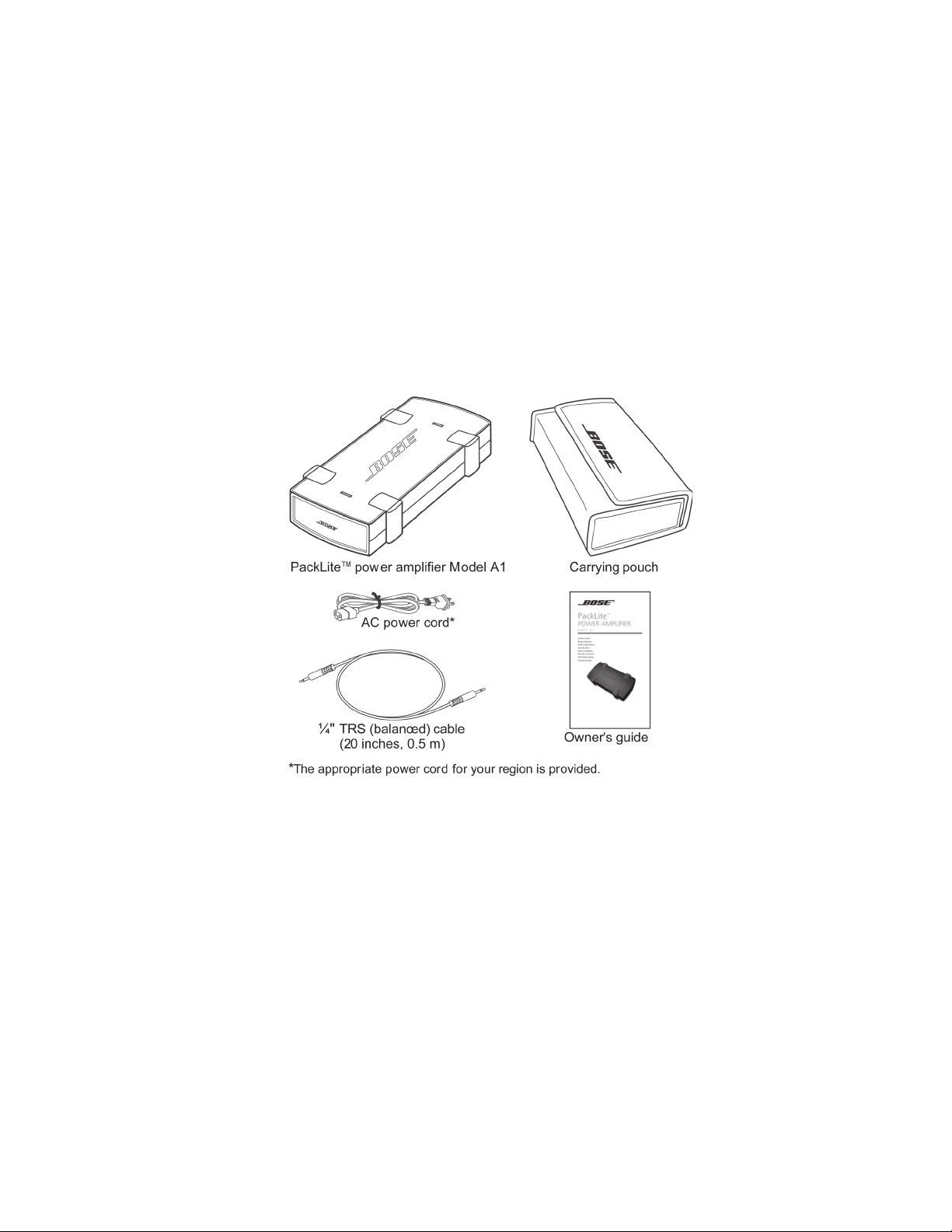
Carton Contents
• Carrying pouch
• PackLite power amplifier Model A1
• AC power cord
• ¼" TRS (balanced) cable (20 inches, 0.5 m)
• Owner’s guide
3
Page 4
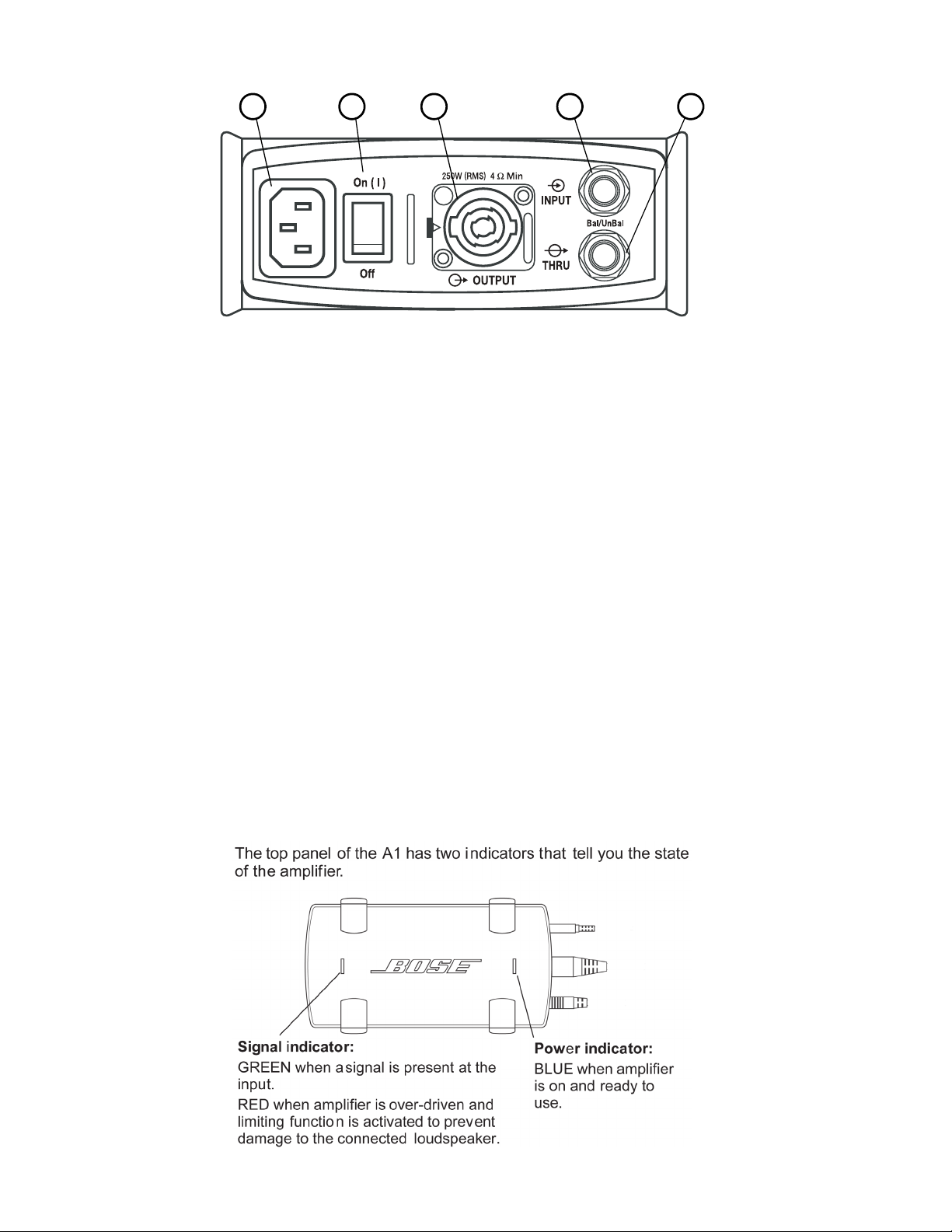
Amplifier Rear Panel Connections and Controls
1 2 3 4 5
1 - AC power connector: Accommodates the supplied AC power cord to connect your amplifier
to the appropriate AC (mains) outlet. Check the product label of your amplifier for the voltage
rating: 120V or 220-240V.
2 - Power switch: In the ON (l) position, applies power to your amplifier. When ON, the power
indicator (see diagram below) should be BLUE.
3 - OUTPUT connector: Accommodates both 2 and 4-wire Neutrik® Speakon® connectors.
OUTPUT can be connected to any of the following:
• B1 bass module.
• 4-ohm loudspeaker with a power rating of at least 250W RMS.
• 8-ohm loudspeaker with a power rating of at least 125W RMS.
4 - INPUT connector: Accommodates a ¼" TRS (balanced) or TS (unbalanced) plug.
INPUT can be connected to either of the following:
• Bass-Line OUT jack on the PS1 power stand using the supplied ¼" TRS cable.
• THRU connector of an “upstream” A1 amplifier when used in series.
• Other line-level source output using either a ¼" TRS or TS cable.
5 - THRU connector: Accommodates a ¼" TRS or TS connection. Used for sending the INPUT
signal to another A1 amplifier.
Notes:
1. Do not use the THRU connector as a second input, as it could damage any interconnected
equipment. Use THRU only as an output to another A1 amplifier.
2. The THRU connector will only relay the type of input (balanced or unbalanced) present at the
INPUT connector.
Top Panel Indicators
4
Page 5
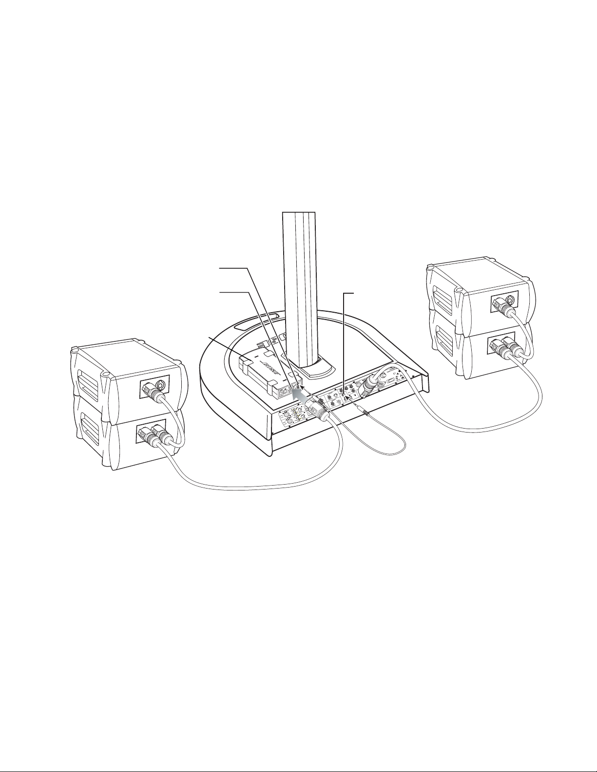
Setting Up a Single A1 Amplifier
The A1 amplifier is designed to add more bass output to a system that already has two B1 bass
modules connected to the Amp 3 OUT connector on the PS1 power stand. The A1 amplifier can
power up to two additional B1 bass modules.
Follow these steps to set up the A1 as shown below.
1. Connect the AC power cord to an AC (mains) outlet.
2. Make sure the A1 amplifier Power switch is OFF.
3. Using the supplied ¼" TRS cable, connect the Bass-Line OUT connector on the PS1 power
stand to the INPUT connector on the A1 amplifier.
4. Connect a B1 bass module cable from the OUTPUT connector on the A1 to a B1 bass module. If desired, connect a second B1 to the first B1.
5. Set the A1 power switch to ON (I).
INPUT
OUTPUT
Bass-Line
OUT
A1 amplifier
B1 bass
modules
PS1 power stand
B1 bass
modules
CAUTION: Do not connect more than two B1 bass modules to an A1 amplifier.
CAUTION: Be careful not to connect the A1 amplifier to a B1 bass module that is already
connected to the Amp 3 OUT connector of a PS1 power stand, or to another A1 amplifier.
Note: Using the supplied ¼" TRS cable with your A1 amplifier is recommended. Using
balanced cabling prevents common interconnect noise problems.
Note: Up to four (maximum) B1 bass modules can be stacked in a column. Stacking may
improve acoustic output.
5
Page 6
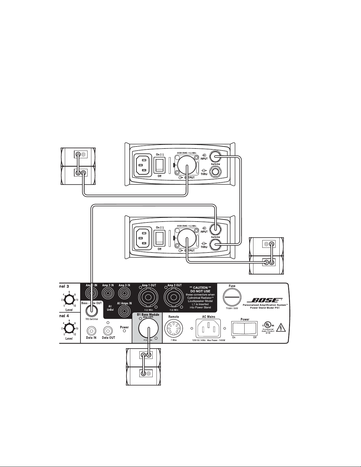
Using Multiple A1 Amplifiers
To add more bass capability to your system, you can connect multiple A1 amplifiers as shown
below.
1. Connect the AC power cord to an AC (mains) outlet.
2. Make sure the Power switch is OFF.
3. Using the supplied ¼" TRS cable, connect the Bass-Line OUT connector on the PS1 power
stand to the INPUT connector on the first A1 amplifier.
4. Using another ¼" TRS cable, connect the THRU connector on the first A1 amplifier to the
INPUT connector of the next A1 amplifier.
5. Connect a B1 bass module to the OUTPUT connector on each A1 amplifier. If desired,
connect a second B1 to the first B1.
6. Set power switch on both A1 amplifiers to ON (I).
B1 bass
modules
2nd
A1
1st
A1
B1 bass
modules
B1 bass
modules
PS1 power stand
CAUTION: Be careful not to connect the A1 amplifier to a B1 bass module that is already
connected to the Amp 3 OUT connector of a PS1 power stand or to another A1 amplifier.
Note: Up to four (maximum) B1 bass modules can be stacked in a column. Stacking may
improve acoustic output.
6
Page 7

Using the A1 in other applications
The A1 amplifier can be used as a power amplifier in other system configurations.
The A1 can drive other passive loudspeakers including subwoofers, floor monitors, studio
monitors, and guitar cabinets. The A1 can amplify a balanced or unbalanced signal from a linelevel device, such as a mixing console, and drive any loudspeaker load (4-ohm minimum) that is
capable of handling 250W.
Setting up the A1 for use with other systems:
1. Make sure the A1 amplifier Power switch is OFF.
2. Connect a line-level output connector from your source device to the INPUT connector of the
A1 amplifier.
• This could be the line-level output from an electronic crossover, mixing console, electric
bass/electric guitar amplifier head unit, preamp, digital modeler, or studio console line
output.
• You can use either a balanced (TRS) or unbalanced (TS) connection. The amplifier will sense
the type of connection and automatically adjust the overall level.
3. Connect the OUTPUT of the A1 amplifier to:
• Any 4-ohm loudspeaker load capable of handling at least 250 watts RMS.
• Any 8-ohm loudspeaker load capable of handling at least 125 watts RMS.
4. If you want to add an additional A1 for more bass, connect the THRU connector of the first A1
to the INPUT connector of another A1 amplifier using a ¼" TRS cable.
5. Set the A1 power switch to ON (I).
6. Adjust the source level so that the A1 signal indicator flashes green. At a maximum source
level, the A1 signal indicator occasionally flashes red. If the indicator is constantly red,
reduce the source level.
Note: Using the A1 amplifier and its connected B1 bass modules with any source device other
than the PS1 power stand is not recommended.
7
Page 8

Specifications
Electrical
Power, 4-ohm load: 250 watts RMS (1 kHz, 0.1% THD)
Power, 8-ohm load: 125 watts RMS (1 kHz, 0.1% THD)
Minimum loudspeaker load: 4 Ohms
Signal to noise: 100 dB (20 Hz to 20 kHz)
Voltage gain: 30 dB
Input sensitivity: 1.15 V (+3.4 dBu)
Input sensing: Automatic, balanced/unbalanced level adjust
Input impedance: 55k ohms unbalanced, 110k ohms balanced
Input clipping: 10 Vrms (+22 dBu)
Frequency response: 20 Hz to 20 kHz ± 0.5 dB
THRU output type: Balanced/unbalanced, dependent on
INPUT connection type
Output circuitry: Class D
Protection types: Self-resetting thermal, output short circuit,
and over-current
Typical AC power requirements: 1.8A, 120VAC; 0.9A, 220-240VAC
Peak inrush current: 28A (120VAC)
Mechanical
Dimensions: 5.6" W x 2.3" H x 10.3" D;
140 mm W x 56 mm H x 258 mm D
Weight: 3.0 lbs (1.4 kg)
Packaged Shipping Weight: 5.0 lbs (2.3 kg)
Max. operating temperature: 122°F (50°C)
8
Page 9

PRODUCTION NOTES
The PackLiteTM A1 amplifier has been manufactured in two versions, a 120V version (product
code 039057) and a 220-240V version (product code 039058).
The early 120V units, serial numbers 039057Z52620201AC to 039057Z52621200AC, are nonRoHS compliant units. 120V units built after the 5262 Julian date (9/19/2005) are fully RoHS
compliant.
The 220-240V version, product code 039058, is fully RoHS compliant from the initial production
units onward.
The Electrical Parts Lists have non-RoHS and RoHS compliant part numbers in cases where
these parts are different for the two versions of the amplifier. Be sure to use ONLY RoHS compliant repair parts in RoHS compliant products.
ELECTROSTATIC DISCHARGE SENSITIVE (ESDS)
DEVICE HANDLING
This unit contains ESDS devices. We recommend the following precautions when repairing,
replacing or transporting ESDS devices:
• Perform work at an electrically grounded work station.
• Wear wrist straps that connect to the station or heel straps that connect to conductive
floor mats.
• Avoid touching the leads or contacts of ESDS devices or PC boards even if properly
grounded. Handle boards by the edges only.
• Transport or store ESDS devices in ESD protective bags, bins, or totes. Do not insert
unprotected devices into materials such as plastic, polystyrene foam, clear plastic bags,
bubble wrap or plastic trays.
PART LIST NOTES
1. This part is not normally available from Customer Service. Approval from the Field Service
Manager is required before ordering.
2. The individual parts located on the PCBs are listed in the Electrical Part List.
3. This part is critical for safety purposes. Failure to use a substitute replacement with the
same safety characteristics as the recommended replacement part might create shock, fire
and/or other hazards.
4. This part is referenced for informational purposes only. It is not stocked as a repair part. Refer
to the next higher assembly for a replacement part.
9
Page 10
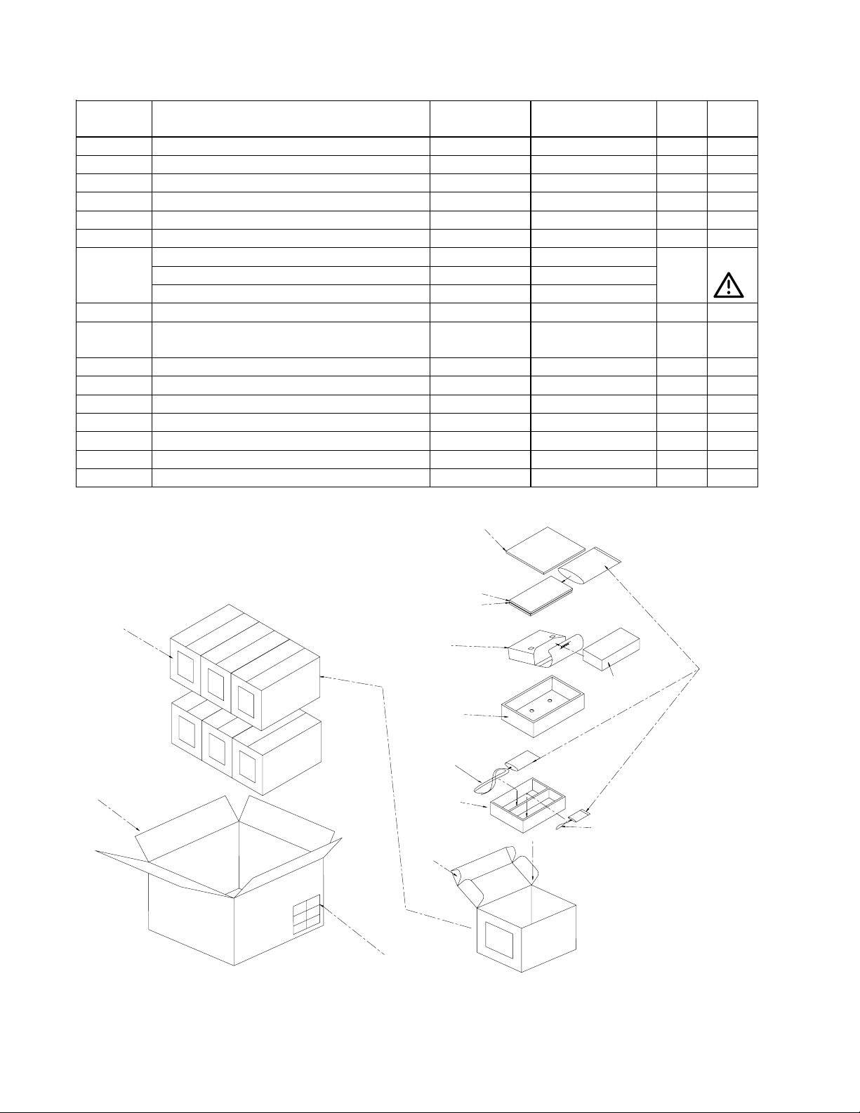
PACKAGING PART LIST
PackLiteTM A1 Amplifier Assembly (see Figure 1)
Item
Number
Description Bose® Part
Number
Vendor Part
Number
Qty. Note
1 Filler, Sheet, 295x168x6, A=B 291589 1450-8830+0 1
2 Owners Manual 287546 4301-7207+0 1
3 Sheet, Warranty / Welcome 287553 3050-3681 1
4 Carry Bag, Nylon 280x150x70 287554 4201-1000+1 1
5 PackLite Amplifier Assembly REF - 1
6 Filler, Lower, 292x167x46 291588 1450-8840+1 1
7 Power Cord, 120V (US/Canada) 263453 - 1 3
Power Cord, L=2.5M, 230V (Europe) 173352 7012-6980+0
Power Cord, 240V (Australia) 264357 -
8 Filler, Upper, 292x167x81 291587 1450-8850+1 1
9 Cable Assy, 1/4" to 1/4", TRS, Stereo
287556 7012-7130+0 1
Signal Input, L=500mm
10 Carton, Single, 4 Color Printed 287550 1480-8201+0 1
11 Carton, Master, 527x304x264mm - 1437-6401+0-2 -
- PE BAG, 8.5x14x0.05 - 1497-4412+0 1
- PE BAG 350x120x0.05 (MIC Cable) - 1497-7762+0 1
- PE BAG 350x120x0.05 (AC Cord) - 1497-7762+0 1
- PE BAG 250x140x0.05 (Manual) - 1497-7772+0 1
- Sheet, Notice - 3050-3701+0 1
INDIVIDUAL AMPS
IN GIFT BOXES
11
1
2
3
4
PE BAGS
5
6
7
8
9
10
Figure 1. PackLite
SKU LABELS (6 UNITS IN
ONE MASTER CARTON)
TM
A1 Amplifier Assembly Packaging View
10
Page 11
MAIN PART LIST
PackLiteTM A1 Amplifier Assembly (see Figure 2)
Item
Number
1 HOUSING, CHASSIS, UPPER,
ALUM, 266x140x28mm
2 INPUT SIGNAL AND LIMITING LED
PCB ASSY,
(PART OF INPUT/LIMITER PCB)
3 BOSE LOGO, ALUM, 40x9.8x1.3mm 288677 2150-7161+0 1
4 FRONT GRILLE, PERFORATED
STEEL, 124x48x0.8mm
5 FAN, DC, 12V, 40x40x10mm 291332 8913-0002+0 1 3
6 FOOT, RUBBER, MOLDED, BLK,
54x26x12mm
7 HEAT TRANSFER PAD, MICA
SHEET, 103x43x0.2mm
8 SMPS/AMPLIFIER PCB ASSEMBLY
(120V Units only)
SMPS/AMPLIFIER PCB ASSEMBLY
(220-240V Units only)
9 INPUT/LIMITER PCB ASSEMBLY 287555 SVC-BS90C11-
10 HOUSING, CHASSIS, LOWER,
ALUM, 266x140x28mm
11 WASHER, SPRING, M3X0.9X5.5, YZ,
(AMP/PS PCB)
12 SCREW, CHASSIS - 2944-3012-3000 4 4
13 LABEL, SAFETY, 120V Units
LABEL, SAFETY, 220-240V Units
14 PC SHEET 1, INSULATING,
128X80X8, T=0.5
15 CONN, NEUTRIK, SPEAKON,
NL4MD-V, (J 117, J118, J119)
16 SWITCH, AC POWER, SPST, TV5,
10A, 250V (120V UNITS)
SWITCH, AC POWER, SPST, 10A,
250V, TV-5 (220-240V UNITS)
17 IEC INLET, AC, 3P, 250V, 15A - 2113-3135+0 1 3
18 I/O PANEL, REAR, BLK, SECC,
123x48x1.2mm
19 POWER AND FAULT LED PCB
ASSEMBLY (PART OF INPUT
/LIMITER PCB)
20 LENS, LED - 3717-2506+0 2
21 PC SHEET 2, INSULATING, UPPER
CHASSIS, 80X65X0.43
- WIRE-CONN 4P P3.96 #18 UL1015
L=200 F (POWER AND FAULT LED
PCB)
- WIRE-CONN 3P P7.92/11.88 #18
UL1015 L=170 F (SIGNAL AND
LIMITING LED PCB)
Description Bose® Part
Number
- 1405-6801+0 1 4
- PCB-
288675 1405-6901+0 1
288673 4157-0981+0 4
291331 3100-6751+1 1
283302 SVC-BS90C11-
291337 SVC-BS90C21-
- 1405-6601+0 1 4
- 2607-3009+0550 4 4
- 3001-0899+0
- 4155-1771+0 1 4
275446 2113-1336+1 1 3
291333 5200-4926 1 3
291335 5200-4926+0
288674 1405-7001+0 1 3
- PCB-
- 4155-1781+0 1 4
- 7012-7042+0 1 4
- 7012-7150+0 1 4
Vendor Part
Number
BS91C21+LED2
AMP
AMP
INP
3001-0900+0
BS91C21+LED1
Qty. Note
1 2, 4
1 2, 3
1 2
1 3
2 2, 4
11
Page 12
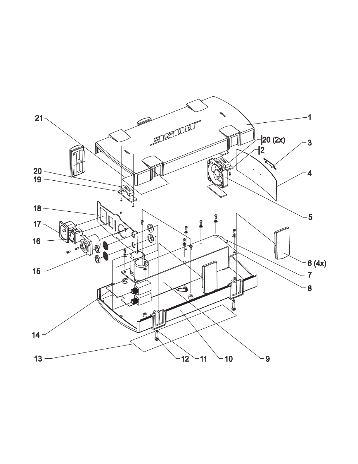
Figure 2. PackLite
TM
A1 Amplifier Exploded View
12
Page 13
ELECTRICAL PART LIST
Power Supply / Amplifier PCB Assembly
Resistors
Reference
Designator
R1 1K, RMG, 0603/1608, 1/16W, 1% 4723-102A+P 4
R3 1K, RMG, 0603/1608, 1/16W, 1% 4723-102A+P 4
R4 10K, RMG, 0603/1608, 1/16W, 1% 4723-103A-P 4
R5 1K, RMG, 0603/1608, 1/16W, 1% 4723-102A+P 4
R6 4.7K, RMG, 0603/1608, 1/16W, 1% 4723-472A-P 4
R7 16K, RMG, 0805, 1/10W, 1% 4720-163A-J 4
R8 12K, RMG, 1206, 1/4W, 1% 4725-123A+6 4
R9 9.1K, RMG, 0805, 1/10W, 1% 4720-912A-J 4
R10 9.1K, RMG, 0805, 1/10W, 1% 4720-912A-J 4
R11 2.2 OHM, RMG, 0603/1608, 1/16W, 5% 4723-2R2J-P 4
R12 2.2 OHM, RMG, 0603/1608, 1/16W, 5% 4723-2R2J-P 4
R13 1M, RMG, 0603/1608, 1/16W, 5% 4723-105J-P 4
R14 1M, RMG, 0603/1608, 1/16W, 5% 4723-105J-P 4
R15 1.5K, RMG, 0603/1608, 1/16W, 1% 4723-152A-P 4
R16 0 OHM, RMG, 0805, 1/10W, 5% 4720-000J+J 4
R17 8.2K, RMG, 0603/1608, 1/16W, 5% 4723-822J+P 4
R18 6.8K, RMG, 0603/1608, 1/16W, 1% 4723-682A-P 4
R19 9.1K, RMG, 0805, 1/10W, 1% 4720-912A-J 4
R20 4.7 OHM, RWR, 5W, 5%, RL 474B-4R7J+5 3, 4
R21 64.9K, RMG, 0603, 1/16W, 1% 4723-6492+P 4
R22 0 OHM, RMG, 0805, 1/10W, 5% 4720-000J+J 4
R23 9.1K, RMG, 0805, 1/10W, 1% 4720-912A-J 4
R24 3.3K, RMG, 0603/1608, 1/16W, 1% 4723-332A-P 4
R25 3.3K, RMG, 0603/1608, 1/16W, 1% 4723-332A-P 4
R26 64.9K, RMG, 0603, 1/16W, 1% 4723-6492+P 4
R27 4.7K, RMG, 0603/1608, 1/16W, 1% 4723-472A-P 4
R28 1K, RMG, 0603/1608, 1/16W, 1% 4723-102A+P 4
R29 12K, RMG, 1206, 1/4W, 1% 4725-123A+6 4
R30 16K, RMG, 0805, 1/10W, 1% 4720-163A-J 4
R31 1.5K, RMG, 0603/1608, 1/16W, 1% 4723-152A-P 4
R32 8.2K, RMG, 0603/1608, 1/16W, 5% 4723-822J+P 4
R34 10 OHM, RMG, 1206, 1/4W, 5% 4725-100J-6 4
R35 10 OHM, RMG, 1206, 1/4W, 5% 4725-100J-6 4
R36 0 OHM, RMG, 0603/1608, 1/16W, 5% 4723-000J-P 4
R38 10 OHM, RMG, 0805, 1/10W, 1% 4720-100A+J 4
R39 10 OHM, RMG, 0805, 1/10W, 1% 4720-100A+J 4
R41 4.7 OHM, RWR, 5W, 5%, RL 474B-4R7J+5 3, 4
R44 10K, RMG, 0603/1608, 1/16W, 1% 4723-103A-P 4
R45 100 OHM, RMG, 0603, 1/16W, 1% 4723-101A+P 4
R46 100 OHM, RMG, 0603, 1/16W, 1% 4723-101A+P 4
R47 100 OHM, RMG, 0603, 1/16W, 1% 4723-101A+P 4
R48 100 OHM, RMG, 0603, 1/16W, 1% 4723-101A+P 4
R49 47K, RMG, 0603/1608, 1/16W, 1% 4723-473A-P 4
Description Vendor Part
Number
Note
13
Page 14

ELECTRICAL PART LIST
Power Supply / Amplifier PCB Assembly
Resistors (continued)
Reference
Designator
R50 47K, RMG, 0603/1608, 1/16W, 1% 4723-473A-P 4
R51 47K, RMG, 0603/1608, 1/16W, 1% 4723-473A-P 4
R52 1.8K, RMG, 0603/1608, 1/16W, 1% 4723-182A-P 4
R53 1K, RMG, 0603/1608, 1/16W, 1% 4723-102A+P 4
R54 1K, RMG, 0603/1608, 1/16W, 1% 4723-102A+P 4
R55 1K, RMG, 0603/1608, 1/16W, 1% 4723-102A+P 4
R56 1K, RMG, 0603/1608, 1/16W, 1% 4723-102A+P 4
R57 47K, RMG, 0603/1608, 1/16W, 1% 4723-473A-P 4
R58 2.2K, RMG, 0603/1608, 1/16W, 1% 4723-222A-P 4
R59 47K, RMG, 0603/1608, 1/16W, 1% 4723-473A-P 4
R60 1.8K, RMG, 0603/1608, 1/16W, 1% 4723-182A-P 4
R61 1K, RMG, 0603/1608, 1/16W, 1% 4723-102A+P 4
R62 1K, RMG, 0603/1608, 1/16W, 1% 4723-102A+P 4
R63 1K, RMG, 0603/1608, 1/16W, 1% 4723-102A+P 4
R64 1K, RMG, 0603/1608, 1/16W, 1% 4723-102A+P 4
R65 47K, RMG, 0603/1608, 1/16W, 1% 4723-473A-P 4
R66 2.2K, RMG, 0603/1608, 1/16W, 1% 4723-222A-P 4
R67 100 OHM, RMG, 0603, 1/16W, 1% 4723-101A+P 4
R68 560 OHM, RMG, 0603, 1/16W, 1% 4723-561A-P 4
R69 2.7K, RMG, 0603/1608, 1/16W, 1% 4723-272A+P 4
R70 2.7K, RMG, 0603/1608, 1/16W, 1% 4723-272A+P 4
R71 2.7K, RMG, 0603/1608, 1/16W, 1% 4723-272A+P 4
R72 2.7K, RMG, 0603/1608, 1/16W, 1% 4723-272A+P 4
R75 2.2 OHM, RMG, 0603/1608, 1/16W, 5% 4723-2R2J-P 4
R76 2.2 OHM, RMG, 0603/1608, 1/16W, 5% 4723-2R2J-P 4
R77 100 OHM, RMG, 0603, 1/16W, 1% 4723-101A+P 4
R78 100 OHM, RMG, 0603, 1/16W, 1% 4723-101A+P 4
R79 100 OHM, RMG, 0603, 1/16W, 1% 4723-101A+P 4
R80 100 OHM, RMG, 0603, 1/16W, 1% 4723-101A+P 4
R81 100 OHM, RMG, 0603, 1/16W, 1% 4723-101A+P 4
R83 100 OHM, RMG, 0603, 1/16W, 1% 4723-101A+P 4
R84 560 OHM, RMG, 0603, 1/16W, 1% 4723-561A-P 4
R85 560 OHM, RMG, 0603, 1/16W, 1% 4723-561A-P 4
R86 560 OHM, RMG, 0603, 1/16W, 1% 4723-561A-P 4
R87 100 OHM, RMG, 0603, 1/16W, 1% 4723-101A+P 4
R88 100 OHM, RMG, 0603, 1/16W, 1% 4723-101A+P 4
R89 100 OHM, RMG, 0603, 1/16W, 1% 4723-101A+P 4
R90 2.2 OHM, RMG, 0603/1608, 1/16W, 5% 4723-2R2J-P 4
R91 2.2 OHM, RMG, 0603/1608, 1/16W, 5% 4723-2R2J-P 4
R92 2.2K, RMG, 0603/1608, 1/16W, 1% 4723-222A-P 4
R93 2.2K, RMG, 0603/1608, 1/16W, 1% 4723-222A-P 4
R94 2.2K, RMG, 0603/1608, 1/16W, 1% 4723-222A-P 4
R95 2.2K, RMG, 0603/1608, 1/16W, 1% 4723-222A-P 4
R100 100K, RMG, 0805, 1/10W, 1% 4720-104A-J 4
R101 100K, RMG, 0805, 1/10W, 1% 4720-104A-J 4
R102 820K, RMG, 0805, 1/10W, 5% 4720-824J-J 4
Description Vendor Part
Number
Note
14
Page 15
ELECTRICAL PART LIST
Power Supply / Amplifier PCB Assembly
Resistors (continued)
Reference
Designator
R103 820K, RMG, 0805, 1/10W, 5% 4720-824J-J 4
R104 820K, RMG, 0805, 1/10W, 5% 4720-824J-J 4
R105 82K, RMG, 0805, 1/10W, 5% 4720-823J-J 4
R106 82K, RMG, 0805, 1/10W, 5% 4720-823J-J 4
R200 10K, RMG, 0603/1608, 1/16W, 1% 4723-103A-P 4
R202 1.5K, RMG, 0603/1608, 1/16W, 1% 4723-152A-P 4
R203 470 OHM, RMG, 0603/1608, 1/16W, 5% 4723-471J-P 4
R204 22 OHM, RMG, 0805, 1/10W, 5% 4720-220J-J 4
R205 22 OHM, RMG, 0805, 1/10W, 5% 4720-220J-J 4
R206 0.15 OHM, 1206, RMG, 1/4W, 5%
(NON-ROHS UNITS)
R206 0.12 OHM, RMG, 1206, 1/4W, 5%
(ROHS COMPLIANT UNITS)
R207 0.15 OHM, 1206, RMG, 1/4W, 5%
(NON-ROHS UNITS)
R207 0.12 OHM, RMG, 1206, 1/4W, 5%
(ROHS COMPLIANT UNITS)
R208 47K, RMG, 0805, 1/10W, 5% 4720-473J-J 4
R209 47K, RMG, 0805, 1/10W, 5% 4720-473J-J 4
R210 47K, RMG, 0805, 1/10W, 5% 4720-473J-J 4
R212 100 OHM, RMG, 0805, 1/10W, 5% 4720-101J-J 4
R213 0.15 OHM, 1206, RMG, 1/4W, 5%
(NON-ROHS UNITS)
R213 0.12 OHM, RMG, 1206, 1/4W, 5%
(ROHS COMPLIANT UNITS)
R214 0.15 OHM, 1206, RMG, 1/4W, 5%
(NON-ROHS UNITS)
R214 0.12 OHM, RMG, 1206, 1/4W, 5%
(ROHS COMPLIANT UNITS)
R215 47K, RMG, 0805, 1/10W, 5% 4720-473J-J 4
R217 470 OHM, RMG, 0603/1608, 1/16W, 5% 4723-471J-P 4
R218 10 OHM, RMG, 0805, 1/10W, 1% 4720-100J+J 4
R219 10 OHM, RMG, 0805, 1/10W, 1% 4720-100J+J 4
R222 1 OHM, RMG, 0603, 1/16W, 5% 4723-1R0J-P 4
R223 1 OHM, RMG, 0603, 1/16W, 5% 4723-1R0J-P 4
R230 10 OHM, RMG, 0805, 1/10W, 1% 4720-100A+J 4
R231 10 OHM, RMG, 0805, 1/10W, 1% 4720-100A+J 4
R232 36K, RMG, 0603, 1/16W, 1% 4723-363A+P 4
Description Vendor Part
Number
4725-R15J+6 3, 4
4725-R12J+6 3, 4
4725-R15J+6 3, 4
4725-R12J+6 3, 4
4725-R15J+6 3, 4
4725-R12J+6 3, 4
4725-R15J+6 3, 4
4725-R12J+6 3, 4
Note
15
Page 16
ELECTRICAL PART LIST
Power Supply / Amplifier PCB Assembly
Resistors (continued)
Reference
Designator
R233 36K, RMG, 0603, 1/16W, 1% 4723-363A+P 4
R234 10K, RMG, 0603/1608, 1/16W, 1% 4723-103A-P 4
R236 10K, RMG, 0603/1608, 1/16W, 1% 4723-103A-P 4
R238 36K, RMG, 0603, 1/16W, 1% 4723-363A+P 4
R239 36K, RMG, 0603, 1/16W, 1% 4723-363A+P 4
R240 47K, RMG, 0603/1608, 1/16W, 1% 4723-473A-P 4
R241 36K, RMG, 0603, 1/16W, 1% 4723-363A+P 4
R242 5.1K, RMG, 0603/1608, 1/16W, 1% 4723-512A+P 4
R243 5.1K, RMG, 0603/1608, 1/16W, 1% 4723-512A+P 4
R290 100K, RMG, 0603, 1/16W, 1% 4723-104A-P 4
R291 100 OHM, RMG, 0603, 1/16W, 1% 4723-101A+P 4
R300 10K, RMG, 1206, 1/8W, 5% 4721-103J+6 4
Reference
Designator
C1 1uF, CC, 0603, 10V, +80/-20% 150C-105Z-P-AC 4
C2 0.47uF, CC, 0805/2012, 16V, 10%, 1.5X2.5 150D-474K+J-BDL 4
C3 1uF, CC, 0603, 10V, +80/-20% 150C-105Z-P-AC 4
C4 1uF, CC, 0603, 10V, +80/-20% 150C-105Z-P-AC 4
C5 2700pF, CC, 0805, 50V, 10%, 1.2X2.0 150F-272K+J-BD 4
C6 47pF, CTC, 0603, 0/60, 5%, 0.8X1.6 15CH-470J-P-AC 4
C7 330pF, CTC, 0603, 0/60, 5%, 0.8X1.6 15CH-331J+P-AC 4
C8 0.22uF, CC, 0805, 16V 10%, 1.2X2.0 150D-224K+J-BD 4
C9 220pF, CTC, 1206, 0/30, 100V, 5% 15CG-221J+6-CFH 4
C10 3300pF, CC, 0805, 50V, 10%, 1.2x2.0 150F-332K-J-BD 4
C11 680pF, CTC, 0805, 0/30, 5%, 1.2x2.5 15CG-681J+J-BD 4
C12 1uF, CC, 0603, 10V, +80/-20% 150C-105Z-P-AC 4
C13 1uF, CC, 0603, 10V, +80/-20% 150C-105Z-P-AC 4
C14 4.7uF, CC, 1206, Y5V, 16V, +80/-20% 150D-475Z+6-CF 4
C15 0.47uF, CM, 100V, 10%, RB, 7.5X8 153H-474K+9-NO 4
C16 0.33uF, CM, 100V, 5%, RBT, 7.5X9.5, MKS2,
WIMA
C17 3300pF, CC, 0805, 50V, 10%, 1.2x2.0 150F-332K-J-BD 4
C18 2700pF, CC, 0805, 50V, 10%, 1.2X2.0 150F-272K+J-BD 4
C19 680pF, CTC, 0805, 0/30, 5%, 1.2x2.5 15CG-681J+J-BD 4
C20 0.22uF, CC, 0805, 16V 10%, 1.2X2.0 150D-224K+J-BD 4
C21 4.7uF, CC, 1206, Y5V, 16V, +80/-20% 150D-475Z+6-CF 4
C22 0.47uF, CM, 100V, 10%, RB, 7.5X8 153H-474K+9-NO 4
C23 220pF, CTC, 1206, 0/30, 100V, 5% 15CG-221J+6-CFH 4
C24 0.33uF, CM, 100V, 5%, RBT, 7.5X9.5, MKS2,
WIMA
C25 2200pF, CC, 0603, 50V, 10%, 0.8x1.6 150F-222K+P-AC 4
C26 2200pF, CC, 0603, 50V, 10%, 0.8x1.6 150F-222K+P-AC 4
C27 47pF, CTC, 0603, 0/60, 5%, 0.8X1.6 15CH-470J-P-AC 4
C28 330pF, CTC, 0603, 0/60, 5%, 0.8X1.6 15CH-331J+P-AC 4
C29 0.47uF, CC, 0805/2012, 16V, 10%, 1.5X2.5 150D-474K+J-BDL 4
Description Vendor Part
Number
Capacitors
Description Vendor Part
Number
153H-334J+V-NRU 4
153H-334J+V-NRU 4
16
Note
Note
Page 17

ELECTRICAL PART LIST
Power Supply / Amplifier PCB Assembly
Capacitors (continued)
Reference
Designator
C31 2.2uF, CC, 1206, 50V, 10%, X7R, MURATA 150F-225K+6-CFM 4
C32 2.2uF, CC, 1206, 50V, 10%, X7R, MURATA 150F-225K+6-CFM 4
C33 1uF, 1206, X7R, CC, 50V, 10%, MURATA
(NON-ROHS UNITS)
C33 2.2uF, CC, 1206, 50V, 10%, X7R, MURATA
(ROHS COMPLIANT UNITS)
C34 1uF, 1206, X7R, CC, 50V, 10%, MURATA
(NON-ROHS UNITS)
C34 2.2uF, CC, 1206, 50V, 10%, X7R, MURATA
(ROHS COMPLIANT UNITS)
C35 0.01uF, CC, 0805, 50V, 20%, 1.2x2.0 150F-103M-J-BD 4
C36 0.01uF, CC, 0805, 50V, 20%, 1.2x2.0 150F-103M-J-BD 4
C37 2.2uF, CC, 1206, 50V, 10%, X7R, MURATA 150F-225K+6-CFM 4
C38 1uF, 1206, X7R, CC, 50V, 10%, MURATA
(NON-ROHS UNITS)
C38 2.2uF, CC, 1206, 50V, 10%, X7R, MURATA
(ROHS COMPLIANT UNITS)
C39 1uF, 1206, X7R, CC, 50V, 10%, MURATA
(NON-ROHS UNITS)
C39 2.2uF, CC, 1206, 50V, 10%, X7R, MURATA
(ROHS COMPLIANT UNITS)
C40 1uF, 1206, X7R, CC, 50V, 10%, MURATA
(NON-ROHS UNITS)
C40 2.2uF, CC, 1206, 50V, 10%, X7R, MURATA
(ROHS COMPLIANT UNITS)
C43 2200uF, 105C, CE, RL, 50V, 20%, 22X25
(NON-ROHS UNITS)
C43 2200uF, CE, 50V, 105C, 20%, RL, 18X31
(ROHS COMPLIANT UNITS)
C44 2200uF, 105C, CE, RL, 50V, 20%, 22X25
(NON-ROHS UNITS)
C44 2200uF, CE, 50V, 105C, 20%, RL, 18X31
(ROHS COMPLIANT UNITS)
C45 220pF, CTC, 0603, 0/60, 5%, 0.8X1.6 15CH-221J+P-AC 4
C46 1uF, CC, 0603, 10V, +80/-20% 150C-105Z-P-AC 4
C47 1uF, CC, 0603, 10V, +80/-20% 150C-105Z-P-AC 4
C48 2.2uF, CM, 50V, 5%, 10X8, METALLIZED 153F-225J+K-SOM 4
C49 2.2uF, CM, 50V, 5%, 10X8, METALLIZED 153F-225J+K-SOM 4
C51 1000pF, CTC, 0805, 0/30, 5%, 1.2x2.5 15CG-102J-J-BD 4
C52 1000pF, CTC, 0805, 0/30, 5%, 1.2x2.5 15CG-102J-J-BD 4
C53 1000pF, CTC, 0805, 0/30, 5%, 1.2x2.5 15CG-102J-J-BD 4
C54 1000pF, CTC, 0805, 0/30, 5%, 1.2x2.5 15CG-102J-J-BD 4
C56 1000pF, CTC, 0805, 0/30, 5%, 1.2x2.5 15CG-102J-J-BD 4
C57 1000pF, CTC, 0805, 0/30, 5%, 1.2x2.5 15CG-102J-J-BD 4
C58 1000pF, CTC, 0805, 0/30, 5%, 1.2x2.5 15CG-102J-J-BD 4
C59 1000pF, CTC, 0805, 0/30, 5%, 1.2x2.5 15CG-102J-J-BD 4
Description Vendor Part
Number
150F-105K+6-CFM 4
150F-225K+6-CFM 4
150F-105K+6-CFM 4
150F-225K+6-CFM 4
150F-105K+6-CFM 4
150F-225K+6-CFM 4
150F-105K+6-CFM 4
150F-225K+6-CFM 4
150F-105K+6-CFM 4
150F-225K+6-CFM 4
157F-228M+5-+&T 4
157F-228M+5-7$T 4
157F-228M+5-+&T 4
157F-228M+5-7$T 4
Note
17
Page 18

ELECTRICAL PART LIST
Power Supply / Amplifier PCB Assembly
Capacitors (continued)
Reference
Designator
C60 220pF, CTC, 0603, 0/60, 5%, 0.8X1.6 15CH-221J+P-AC 4
C61 220pF, CTC, 0603, 0/60, 5%, 0.8X1.6 15CH-221J+P-AC 4
C62 220pF, CTC, 0603, 0/60, 5%, 0.8X1.6 15CH-221J+P-AC 4
C63 1000pF, CTC, 0805, 0/30, 5%, 1.2x2.5 15CG-102J-J-BD 4
C68 0.1uF, CC, 0603/1608, 50V, 10%, 1x2 150F-104K-P-AC 4
C100 0.33uF, CM, 300V, 10%, RB, 18X15.5X10 1511-334K+9-03Z 3, 4
C103 0.015uF, CC, 1206, X7R, 630V, 10% 150M-153K+6-CF 4
C104 0.015uF, CC, 1206, X7R, 630V, 10% 150M-153K+6-CF 4
C105 0.015uF, CC, 1206, X7R, 630V, 10% 150M-153K+6-CF 4
C106 0.015uF, CC, 1206, X7R, 630V, 10% 150M-153K+6-CF 4
C107 680uF, CE, 200V, 105C, 20%, RL, 25X35 157U-687M+5-&^T 4
C108 680uF, CE, 200V, 105C, 20%, RL, 25X35 157U-687M+5-&^T 4
C109 1000pF, CC, 400V, 20%, RL, 9X6 150T-102M+5-QK 3, 4
C110 1000pF, CC, 400V, 20%, RL, 9X6 150T-102M+5-QK 3, 4
C111 2200pF, CC, 400V, 20%, RL, 10X6 150T-222M+5-SK 3, 4
C112 0.33uF, CM, 300V, 10%, RB, 18X15.5X10 1511-334K+9-03Z 3, 4
C200 680pF, CTC, 0603, 0/60, 5% 15CH-681J+P-AC 4
C201 0.22uF, CC, 0805, 16V 10%, 1.2X2.0 150D-224K+J-BD 4
C202 0.47uF, CM, 400VDC, 5%, RB, 18X17.5X9 1511-474J+9-0T 4
C203 0.47uF, CM, 400VDC, 5%, RB, 18X17.5X9 1511-474J+9-0T 4
C204 1uF, CC, 0805, 25V, 10% 150E-105K+J-BD 4
C205 1uF, CC, 0805, 25V, 10% 150E-105K+J-BD 4
C206 1uF, 1206, X7R, CC, 50V, 10%, MURATA
(NON-ROHS UNITS)
C206 2.2uF, CC, 1206, 50V, 10%, X7R, MURATA
(ROHS COMPLIANT UNITS)
C207 1uF, 1206, X7R, CC, 50V, 10%, MURATA
(NON-ROHS UNITS)
C207 2.2uF, CC, 1206, 50V, 10%, X7R, MURATA
(ROHS COMPLIANT UNITS)
C208 1uF, CC, 1206, X7R, 50V, 10%, MURATA 150F-105K+6-CFM 4
C210 470pF, CC, 2211, 250VAC, 10%, 2.8X5.7 150R-471K+Y-EKZ 3, 4
C211 1uF, CC, 1206, X7R, 50V, 10%, MURATA 150F-105K+6-CFM 4
Description Vendor Part
Number
150F-105K+6-CFM 4
150F-225K+6-CFM 4
150F-105K+6-CFM 4
150F-225K+6-CFM 4
Note
18
Page 19

ELECTRICAL PART LIST
Power Supply / Amplifier PCB Assembly
Capacitors (continued)
Reference
Designator
C212 470pF, CC, 2211, 250VAC, 10%, 2.8X5.7 150R-471K+Y-EKZ 3, 4
C213 470pF, CC, 2211, 250VAC, 10%, 2.8X5.7 150R-471K+Y-EKZ 3, 4
C214 100pF, CC, 0603/1608, 50V, 5%, 1X2 150F-101J-P-AC 4
C215 100pF, CC, 0603/1608, 50V, 5%, 1X2 150F-101J-P-AC 4
C216 1000pF, CTC, 0805, 0/30, 5%, 1.2x2.5 15CG-102J-J-BD 4
C217 1000pF, CTC, 0805, 0/30, 5%, 1.2x2.5 15CG-102J-J-BD 4
C218 470pF, CC, 2211, 250VAC, 10%, 2.8X5.7 150R-471K+Y-EKZ 3, 4
C219 1uF, CC, 1206, X7R, 50V, 10%, MURATA 150F-105K+6-CFM 4
C220 1uF, CC, 0603, 10V, +80/-20% 150C-105Z-P-AC 4
C221 1uF, CC, 0603, 10V, +80/-20% 150C-105Z-P-AC 4
C222 470uF, CE, 35V, 105C, 20%, RL, 10X20 157Q-477M+5-S9T 4
C223 470uF, CE, 35V, 105C, 20%, RL, 10X20 157Q-477M+5-S9T 4
C226 0.15uF, CC, 0805, 50V, 10% 150F-154K+J-BD 4
C227 0.15uF, CC, 0805, 50V, 10% 150F-154K+J-BD 4
C300 0.01uF, CC, 1206, 50V, 10%, 1.6x3.2 150F-103K-6-CF 4
Description Vendor Part
Number
Inductors
Note
Reference
Designator
L1 CHOKE, COIL, 10uH, 10%, 7A, T94-2 1806-3899+0 4
L3 CHOKE, COIL, 10uH, 10%, 7A, T94-2 1806-3899+0 4
L6 FERRITE BEAD INDUCTOR, BL01RN1A1F1J 1808-0680-0 4
L7 FERRITE BEAD INDUCTOR, BL01RN1A1F1J 1808-0680-0 4
L8 CHOKE, COMMON MODE, 2X16uH, 8A, FT50-
43
L100 CHOKE, COMMON MODE, 3A, 2X15MH, TC-
2510 (NON-ROHS UNITS)
L100 CHOKE, COMMON MODE, 2X10mH, 3A, TC-
2510 (ROHS COMPLIANT UNITS)
L101 CHOKE, COMMON MODE, 2X10mH, 3A, TC-
2510
L200 INDUCTOR, 10uH, 500MA, SMD, 1210 1803-0092+0 4
L201 INDUCTOR, 10uH, 500MA, SMD, 1210 1803-0092+0 4
Description Vendor Part
Number
1806-3913+0 4
1806-3901+1 3, 4
1806-3934+0 3, 4
1806-3934+0 3, 4
Note
19
Page 20

ELECTRICAL PART LIST
Power Supply / Amplifier PCB Assembly
Diodes
Reference
Designator
D1 BAS321, 200V, 250MA, 50NS, SOD323 480S-3210+3 4
D2 BAS321, 200V, 250MA, 50NS, SOD323 480S-3210+3 4
D3 BAS321, 200V, 250MA, 50NS, SOD323 480S-3210+3 4
D4 BAS321, 200V, 250MA, 50NS, SOD323 480S-3210+3 4
D5 BAS321, 200V, 250MA, 50NS, SOD323 480S-3210+3 4
D6 BAS321, 200V, 250MA, 50NS, SOD323 480S-3210+3 4
D7 BAS321, 200V, 250MA, 50NS, SOD323 480S-3210+3 4
D8 BAS321, 200V, 250MA, 50NS, SOD323 480S-3210+3 4
D9 BAS321, 200V, 250MA, 50NS, SOD323 480S-3210+3 4
D10 BAS321, 200V, 250MA, 50NS, SOD323 480S-3210+3 4
D14 BAS321, 200V, 250MA, 50NS, SOD323 480S-3210+3 4
D100 BRIDGE, GBU8J, 600V, 8A, RL
(NON-ROHS UNITS)
D100 DIODE BRIDGE, 800V, 8A, GBU8K, RL
(ROHS COMPLIANT UNITS)
D200 US1J, 600V, 1A, 75NS, SOD124 480U-S1J0+3 4
D201 BAS216, 75V, 250MA, 4NS, SOD110 480S-2160+3 4
D202 BAS216, 75V, 250MA, 4NS, SOD110 480S-2160+3 4
D203 BAS216, 75V, 250MA, 4NS, SOD110 480S-2160+3 4
D204 BAS216, 75V, 250MA, 4NS, SOD110 480S-2160+3 4
D205 12CWQ10FNTRBF, RECTIFIER, 100V, 12A,
DPAK, SMDIR
D206 12CWQ10FNTRBF, RECTIFIER, 100V, 12A,
DPAK, SMDIR
D207 12CWQ10FNTRBF, RECTIFIER, 100V, 12A,
DPAK, SMDIR
D208 12CWQ10FNTRBF, RECTIFIER, 100V, 12A,
DPAK, SMDIR
D209 RS1D, RECTIFIER, 200V, 1A, SOD124 4840-9212+3 4
D210 RS1D, RECTIFIER, 200V, 1A, SOD124 4840-9212+3 4
D211 BAS216, 75V, 250MA, 4NS, SOD110 480S-2160+3 4
D212 BAS216, 75V, 250MA, 4NS, SOD110 480S-2160+3 4
D216 BAS216, 75V, 250MA, 4NS, SOD110 480S-2160+3 4
D217 BAS216, 75V, 250MA, 4NS, SOD110 480S-2160+3 4
D218 BAS216, 75V, 250MA, 4NS, SOD110 480S-2160+3 4
D290 BAS216, 75V, 250MA, 4NS, SOD110 480S-2160+3 4
Z200 ZENER, 15V, 0.4W, BZX284-B15 4840-9230+0 4
Z201 ZENER, BZX284-C11@115, 11V, 1/2W, DZ,
SOD110
Description Vendor Part
Number
4840-9211+5 3, 4
4840-9218+5 3, 4
4840-9213+3 4
4840-9213+3 4
4840-9213+3 4
4840-9213+3 4
4837-1109+3 4
Note
20
Page 21

ELECTRICAL PART LIST
Reference
Description Vendor Part
Note
Reference
Description Vendor Part
Note
Power Supply / Amplifier PCB Assembly
Transistors
Designator
Q1 FDD368, MOSFET, N-CHANNEL, 2_NL, 100V,
32A, TO-252AA (Bose
Q2 FDD368, MOSFET, N-CHANNEL, 2_NL, 100V,
32A, TO-252AA (Bose part number 291330)
Q3 FDD368, MOSFET, N-CHANNEL, 2_NL, 100V,
32A, TO-252AA (Bose part number 291330)
Q4 FDD368, MOSFET, N-CHANNEL, 2_NL, 100V,
32A, TO-252AA (Bose part number 291330)
Q5 BC856S, PNP PAIR, 60V, SOT363 4858-56S0+3 4
Q6 BC856S, PNP PAIR, 60V, SOT363 4858-56S0+3 4
Q200 STB12NM50FD, MOSFET, N-CHANNEL,
D2PAK (Bose part number 291329)
Q201 STB12NM50FD, MOSFET, N-CHANNEL,
D2PAK (Bose part number 291329)
Q202 REGULATOR, 5V, LM78L05ACM, SO-8 3131-3390+0 4
Q203 BCP56-10, NPN, SOT223 485C-P560+3 4
Q204 REGULATOR, 250MA, LM79L05, SO8 3132-3091+0 4
Q205 FFB2227A, NPN/PNP PAIR, SC70-6 4852-27A0+3 4
Q206 FFB2227A, NPN/PNP PAIR, SC70-6 4852-27A0+3 4
Q207 BC856S, PNP PAIR, 60V, SOT363 4858-56S0+3 4
Q208 2N7002MTF, MOSFET, N-CHANNEL, SOT-23 4902-MTF0- 3 4
Q209 2N7002MTF, MOSFET, N-CHANNEL, SOT-23 4902-MTF0- 3 4
Q210 BC856S, PNP PAIR, 60V, SOT363 4858-56S0+3 4
Q211 BC846B, SOT23, PHILIPS, SMD 4858-46B0+3 4
Q290 PUMZ1, NPN/PNP PAIR, SOT363 485U-MZ10+3 4
®
part number 291330)
Number
4903-6820+3
4903-6820+3
4903-6820+3
4903-6820+3
4905-0FD0+3
4905-0FD0+3
Integrated Circuits
Designator
IC1 HALF BRIDGE DRIVER, LV4970M, SO-16 3132-3051+0 4
IC2 HALF BRIDGE DRIVER, LV4970M, SO-16 3132-3051+0 4
IC3 ANALOG 2CH CONTROLLER, LV4930M,
QUAD44
IC4 OP-AMP, MC33078DR2G, SO-8 3132-2711+0 4
IC200 HALF BRIDGE DRIVER, L6571BD013TR, SO8
(Bose part number 291328)
Number
3132-3061+0 4
3132-3071+0
21
Page 22

ELECTRICAL PART LIST
Power Supply / Amplifier PCB Assembly
Miscellaneous
Reference
Designator
F100 FUSE, T6.3A/125V, TE5-T, PSE/UL
(120V UNITS)
F100 FUSE, T3.15A, 250V, 8.5X8, VDE/UL/SEMKO,
TR5-T (220-240V UNITS)
F200 0 OHM, RMG, 1206, 1/8W, 1% 4721-000A+6 3, 4
MOV1 VARISTOR, 175V, SIOV-S05K175
(NON-ROHS UNITS)
MOV2 VARISTOR, 175V, SIOV-S05K175
(NON-ROHS UNITS)
MOV VARISTOR, 320V, 10%, SIOV-S10K320
(ROHS COMPLIANT UNITS)
N1 THERMISTOR, NTC, 100K, 5,% B5,
7620C0104J162, 0805, EPCOS
N100 NTC THERMISTOR, 5 0HM, 4A, NIOSP005L,
UL/CSA/VDE
N101 NTC THERMISTOR, 5 0HM, 4A, NIOSP005L,
UL/CSA/VDE
N200 THERMISTOR, PTC, 1K, 0805, 90 DEG, EPCOS 5202-0011+0 4
N201 THERMISTOR, PTC, 1K, 130 DEG, 0805,
EPCOS
S100 WJ, #23, 120/220-240V SELECTOR JUMPER.
(USED ON 120V UNITS ONLY)
S302 WJ, #23 635N-0001-0 4
TRAFO200 TRANSFORMER, SWITCHING, ETD29 1806-3898+0 3, 4
CON300 WAFER, 3P, P7.92/11.88, STRAIGHT 2101-3097+0 3, 4
CON301 WAFER, 4P, P3.96 (NON-ROHS UNITS) 2101-3053-0 4
CON301 WAFER, 4P, P3.96 (ROHS COMPLIANT UNITS) 2101-3053+0 4
J301 6 PIN, WF 2102-060S+003 4
J302 6 PIN, WF 2102-060S+003 4
J303 WAFER, 3P, P2.0, ST, MALE 2101-3008+0 4
JP1 WIRE JUMPER, ROLLER FORM, D=0.6MM
(ROHS COMPLIANT UNITS)
JP2 WIRE JUMPER, ROLLER FORM, D=0.6MM
(ROHS COMPLIANT UNITS)
Description Vendor Part
Number
5120-1094+0 3, 4
5120-0087+0 3, 4
4735-0002+0 3, 4
4735-0002+0 3, 4
4735-0003+0 3, 4
5202-0019+0 4
5202-0010+0 3, 4
5202-0010+0 3, 4
5202-0021+0 4
635N-0001-0 4
635N-0002+0 4
635N-0002+0 4
Note
22
Page 23

ELECTRICAL PART LIST
Input / Limiter PCB Assembly
Resistors
Reference
Designator
R301 39K, RMG, 0805, 1/10W, 1% 4720-393A+J 4
R302 39K, RMG, 0805, 1/10W, 1% 4720-393A+J 4
R303 24K, RMG, 0805, 1/10W, 5% 4720-243J+J 4
R304 100 OHM, RMG, 0805, 1/10W, 5% 4720-101J+J 4
R305 10K, RMG, 0805, 1/10W, 5% 4720-103J+J 4
R306 39K, RMG, 0805, 1/10W, 1% 4720-393A+J 4
R307 10K, RMG, 0805, 1/10W, 5% 4720-103J+J 4
R308 82K, RMG, 0805, 1/10W, 1% 4720-823A+J 4
R309 39K, RMG, 0805, 1/10W, 1% 4720-393A+J 4
R310 200K, RMG, 0805, 1/10W, 5% 4720-204J+J 4
R311 20K, RMG, 0805, 1/10W, 1% 4720-203A+J 4
R312 82K, RMG, 0805, 1/10W, 1% 4720-823A+J 4
R313 39K, RMG, 0805, 1/10W, 1% 4720-393A+J 4
R314 24K, RMG, 0805, 1/10W, 5% 4720-243J+J 4
R315 39K, RMG, 0805, 1/10W, 1% 4720-393A+J 4
R316 39K, RMG, 0805, 1/10W, 1% 4720-393A+J 4
R317 7.5K, RMG, 0805, 1/10W, 1% 4720-752A+J 4
R318 33K, RMG, 0805, 1/10W, 5% 4720-333J+J 4
R319 100K, RMG, 0805, 1/10W, 5% 4720-104J+J 4
R320 200K, RMG, 0805, 1/10W, 5% 4720-204J+J 4
R321 39K, RMG, 0805, 1/10W, 1% 4720-393A+J 4
R322 100 OHM, RMG, 0805, 1/10W, 5% 4720-101J+J 4
R323 22 OHM, RMG, 0805, 1/10W, 5% 4720-220J+J 4
R324 20K, RMG, 0805, 1/10W, 1% 4720-203J+J 4
R325 10K, RMG, 0805, 1/10W, 5% 4720-103J+J 4
R326 100K, RMG, 0805, 1/10W, 5% 4720-104J+J 4
R327 47K, RMG, 0805, 1/10W, 5% 4720-473J+J 4
R328 1K, RMG, 0805, 1/10W, 5% 4720-102J+J 4
R329 36K, RMG, 0805, 1/10W, 5% 4720-363J+J 4
R330 10K, RMG, 0805, 1/10W, 5% 4720-103J+J 4
R331 22 OHM, RMG, 0805, 1/10W, 5% 4720-220J+J 4
R333 750K, RMG, 0805, 1/10W, 5% 4720-754J+J 4
R334 510 OHM, RMG, 0805, 1/10W, 5% 4720-511J+J 4
R335 10K, RMG, 0805, 1/10W, 5% 4720-103J+J 4
R336 20K, RMG, 0805, 1/10W, 1% 4720-203J+J 4
R337 10K, RMG, 0805, 1/10W, 5% 4720-103J+J 4
R338 22K, RMG, 0805, 1/10W, 5% 4720-223J+J 4
R339 30K, RMG, 0805, 1/10W, 1% 4720-303J+J 4
R340 200K, RMG, 0805, 1/10W, 5% 4720-204J+J 4
R341 200K, RMG, 0805, 1/10W, 5% 4720-204J+J 4
R342 39K, RMG, 0805, 1/10W, 1% 4720-393A+J 4
R343 150K, RMG, 0805, 1/10W, 5% 4720-154J+J 4
R344 91K, RMG, 0805, 1/10W, 1% 4720-913A+J 4
R345 30K, RMG, 0805, 1/10W, 1% 4720-303J+J 4
R346 510 OHM, RMG, 0805, 1/10W, 5% 4720-511J+J 4
R347 39K, RMG, 0805, 1/10W, 1% 4720-393A+J 4
Description Vendor Part
Number
Note
23
Page 24

ELECTRICAL PART LIST
Input / Limiter PCB Assembly
Resistors (continued)
Reference
Designator
R348 2.7K, RMG, 0805, 1/10W, 1% 4720-272A+J 4
R349 750K, RMG, 0805, 1/10W, 5% 4720-754J+J 4
R350 30K, RMG, 0805, 1/10W, 1% 4720-303A+J 4
R351 0 OHM, RMG, 0805, 1/10W, 5% 4720-000J+J 4
R352 51 OHM, RCF, 1/4W, 5%, AT 4705-510J+2 4
R355 5.1K, RMG, 0805, 1/10W, 5% 4720-512J+J 4
R356 2.2K, RMG, 0805, 1/10W, 1% 4720-222J+J 4
R360 100 OHM, RMG, 0805, 1/10W, 5% 4720-101J+J 4
R361 49.9K, RMG, 0805, 1/10W, 1% 4720-4992+J 4
R362 510 OHM, RMG, 0805, 1/10W, 5% 4720-511J+J 4
R363 510 OHM, RMG, 0805, 1/10W, 5% 4720-511J+J 4
R364 1K, RMG, 0805, 1/10W, 5% 4720-102J+J 4
R365 10K, RMG, 0805, 1/10W, 5% 4720-103J+J 4
R366 150K, RMG, 0805, 1/10W, 5% 4720-154J+J 4
R367 51 OHM, RCF, 1/4W, 5%, AT 4705-510J+2 4
R368 39K, RMG, 0805, 1/10W, 1% 4720-393A+J 4
R369 12K, RMG, 0805, 1/10W, 1% 4720-123A+J 4
R370 2.2K, RMG, 0805, 1/10W, 1% 4720-222A+J 4
R377 510K, RMG, 0805, 1/10W, 5% 4720-514J+J 4
R378 2.2K, RMG, 0805, 1/10W, 1% 4720-222A+J 4
R379 39K, RMG, 0805, 1/10W, 1%
(ROHS COMPLIANT UNITS)
Description Vendor Part
Number
4720-393A+J 4
Capacitors
Note
Reference
Designator
C301 10uF, CE, 50V, 20%, RLT, 4X7 157F-106M+K-GM 4
C302 27pF, CTC, 0805, 0/30, 5%, 1.2X2.5 15CG-270J+J-BD 4
C303 10uF, CE, 50V, 20%, RLT, 4X7 157F-106M+K-GM 4
C304 100pF, CTC, 0805, 0/30, 5%, 1.2x2.5 15CG-101J+J-BD 4
C305 68pF, CC, 0805, 50V, 5%, 1.25X2.0, MURATA 150F-680J+J-BDM 4
C306 10uF, CE, 50V, 20%, RLT, 4X7 157F-106M+K-GM 4
C307 100pF, CTC, 0805, 0/30, 5%, 1.2x2.5 15CG-101J+J-BD 4
C308 100pF, CTC, 0805, 0/30, 5%, 1.2x2.5 15CG-101J+J-BD 4
C309 68pF, CC, 0805, 50V, 5%, 1.25X2.0, MURATA 150F-680J+J-BDM 4
C310 10uF, CE, 50V, 20%, RLT, 4X7 157F-106M+K-GM 4
C311 27pF, CTC, 0805, 0/30, 5%, 1.2X2.5 15CG-270J+J-BD 4
C312 10uF, CE, 50V, 20%, RLT, 4X7 157F-106M+K-GM 4
C313 47pF, CTC, 0805, 0/60, 5%, 1.2X2.5, 100V 15CH-470J+J-BD 4
C314 100pF, CTC, 0805, 0/30, 5%, 1.2x2.5 15CG-101J+J-BD 4
C315 20pF, 0805, CTC, 0/30, 5%, 1.2x2.5
(NON-ROHS UNITS)
C315 22pF, CTC, 0805, 0/60, 5%, 1.2X2.5
(ROHS COMPLIANT UNITS)
C316 100pF, CTC, 0805, 0/30, 5%, 1.2x2.5 15CG-101J+J-BD 4
C317 220pF, CC, 0805, 50V, 10%, 1.2x2.0 150F-221K+J-BD 4
C318 10uF, CE, 50V, 20%, RLT, 4X7 157F-106M+K-GM 4
Description Vendor Part
Number
15CG-200J-J-BD 4
15CH-220J+J-BD 4
Note
24
Page 25

ELECTRICAL PART LIST
Input / Limiter PCB Assembly
Capacitors (continued)
Reference
Designator
C319 1000pF, CTC, 0805, 0/30, 5%, 1.2x2.5 15CG-102J+J-BD 4
C320 1000pF, CTC, 0805, 0/30, 5%, 1.2x2.5 15CG-102J+J-BD 4
C321 1000pF, CTC, 0805, 0/30, 5%, 1.2x2.5 15CG-102J+J-BD 4
C322 1000pF, CTC, 0805, 0/30, 5%, 1.2x2.5 15CG-102J+J-BD 4
C323 1000pF, CTC, 0805, 0/30, 5%, 1.2x2.5 15CG-102J+J-BD 4
C324 1000pF, CTC, 0805, 0/30, 5%, 1.2x2.5 15CG-102J+J-BD 4
C328 10uF, CE, 50V, 20%, RLT, 4X7 157F-106M+K-GM 4
C329 1.0pF, CTC, 0805, 0/30, 50V, 1.2X2.5 15CG-1R0C+J-
C330 100pF, CTC, 0805, 0/30, 5%, 1.2x2.5 15CG-101J+J-BD 4
C331 47uF, CE, 25V, 20%, RLT, 5X11, ELNA 157E-476M+K-IUE 4
C332 1000pF, CTC, 0805, 0/30, 5%, 1.2x2.5 15CG-102J+J-BD 4
C333 1000pF, CTC, 0805, 0/30, 5%, 1.2x2.5 15CG-102J+J-BD 4
C334 1000pF, CTC, 0805, 0/30, 5%, 1.2x2.5 15CG-102J+J-BD 4
C335 1000pF, CTC, 0805, 0/30, 5%, 1.2x2.5 15CG-102J+J-BD 4
C336 1000pF, CTC, 0805, 0/30, 5%, 1.2x2.5 15CG-102J+J-BD 4
C337 1000pF, CTC, 0805, 0/30, 5%, 1.2x2.5 15CG-102J+J-BD 4
C338 1000pF, CTC, 0805, 0/30, 5%, 1.2x2.5 15CG-102J+J-BD 4
C343 2.2uF, CE, 50V, 20%, RLT, 4X7, ELNA 157F-225M+K-
C344 1uF, CC, 0805, 25V, 10% 150E-105K+J-BD 4
C345 1uF, CE, 50V, 20%, RLT, 4X7 157F-105M+K-GM 4
C346 47uF, CE, 25V, 20%, RLT, 5X11, ELNA 157E-476M+K-IUE 4
C347 47uF, CE, 25V, 20%, RLT, 5X11, ELNA 157E-476M+K-IUE 4
C350 10uF, CE, 50V, 20%, RLT, 4X7 157F-106M+K-GM 4
C352 0.1uF, CC, 0805, 50V, 20%, 1.2x2.0 150F-104M+J-BD 4
C353 22uF, CE, 25V, 20%, RLT, 5X11 157E-226M+K-IU 4
C354 0.1uF, CC, 0805, 50V, 20%, 1.2x2.0 150F-104M+J-BD 4
C355 22uF, CE, 25V, 20%, RLT, 5X11 157E-226M+K-IU 4
C356 10uF, CE, 50V, 20%, RLT, 4X7 157F-106M+K-GM 4
C357 0.1uF, CC, 0805, 50V, 20%, 1.2x2.0 150F-104M+J-BD 4
C358 10uF, CE, 50V, 20%, RLT, 4X7 157F-106M+K-GM 4
C359 0.1uF, CC, 0805, 50V, 20%, 1.2x2.0 150F-104M+J-BD 4
C360 100pF, CTC, 0805, 0/30, 5%, 1.2x2.5 15CG-101J+J-BD 4
C361 10uF, CE, 50V, 20%, RLT, 4X7 157F-106M+K-GM 4
C362 0.47uF, CC, 0805, 25V, 20% 150E-474M+J-BD 4
C363 47uF, CE, 25V, 20%, RLT, 5X11, ELNA 157E-476M+K-IUE 4
C364 1000pF, 50V, 0805, CC, 10%, 1.2x2.0
(NON-ROHS UNITS)
C365 1000pF, 50V, 0805, CC, 10%, 1.2x2.0
(NON-ROHS UNITS)
C366 1000pF, 50V, 0805, CC, 10%, 1.2x2.0
(NON-ROHS UNITS)
C367 1000pF, 50V, 0805, CC, 10%, 1.2x2.0
(NON-ROHS UNITS)
C368 220uF, CE, 16V, 20%, RLT, 6.3X11, SC, SHOEI 157D-227M+K-LUI 4
C369 2.2uF, CE, 50V, 20%, RLT, 4X7, ELNA 157F-225M+K- 4
Description Vendor Part
Number
BDF
GMK
150F-102K-J-BD 4
150F-102K-J-BD 4
150F-102K-J-BD 4
150F-102K-J-BD 4
Note
4
4
25
Page 26

ELECTRICAL PART LIST
Input / Limiter PCB Assembly
Diodes
Reference
Designator
D301 1N4148T, AT 4804-1480+2 4
D302 1N4148T, AT 4804-1480+2 4
D303 1N4148T, AT 4804-1480+2 4
D304 1N4148T, AT 4804-1480+2 4
D305 1N4148, AT (NON-ROHS UNITS) 4804-1480-2 4
D305 ZENER, 12V, 1/2W, 5%, AT, TEMIC
(ROHS COMPLIANT UNITS)
D306 1N4148, AT (NON-ROHS UNITS) 4804-1480-2 4
D306 ZENER, 12V, 1/2W, 5%, AT, TEMIC
(ROHS COMPLIANT UNITS)
D307 ZENER, 5.1V, 1/2W, AT, TEMIC 4837-5V16+2 4
D308 SCHOTTKY, BAT42-T, DO-35, AT 480A-T420+2 4
D309 1N4148T, AT 4804-1480+2 4
D310 ZENER, 12V, 1/2W, 5%, AT, TEMIC 4837-1206+2 4
D319 ZENER, 3V, 1/2W, 5%, MMSZ4683T1, SOD-123 4837-3V09+3 4
D320 ZENER, 3V, 1/2W, 5%, MMSZ4683T1, SOD-123 4837-3V09+3 4
Reference
Designator
Q301 2N3904, RLT (NON-ROHS UNITS) 4853-9040-K 4
Q301 2N3904TA, RLT (ROHS COMPLIANT UNITS) 4853-9040+K 4
Q302 2N3904, RLT (NON-ROHS UNITS) 4853-9040-K 4
Q302 2N3904TA, RLT (ROHS COMPLIANT UNITS) 4853-9040+K 4
Q303 2N3904, RLT (NON-ROHS UNITS) 4853-9040-K 4
Q303 2N3904TA, RLT (ROHS COMPLIANT UNITS) 4853-9040+K 4
Q304 2N3906, RLT, TO92, PHILIPS
(NON-ROHS UNITS)
Q304 2N3906, RLT, TO92, PHILIPS
(ROHS COMPLIANT UNITS)
Q305 2N3904, RLT (NON-ROHS UNITS) 4853-9040-K 4
Q305 2N3904TA, RLT (ROHS COMPLIANT UNITS) 4853-9040+K 4
Q306 2N3904, RLT (NON-ROHS UNITS) 4853-9040-K 4
Q306 2N3904TA, RLT (ROHS COMPLIANT UNITS) 4853-9040+K 4
Q307 2N3904, RLT (NON-ROHS UNITS) 4853-9040-K 4
Q307 2N3904TA, RLT (ROHS COMPLIANT UNITS) 4853-9040+K 4
Q308 2N3906, RLT, TO92, PHILIPS
(NON-ROHS UNITS)
Q308 2N3906, RLT, TO92, PHILIPS
(ROHS COMPLIANT UNITS)
Q309 2N3904, RLT (NON-ROHS UNITS) 4853-9040-K 4
Q309 2N3904TA, RLT (ROHS COMPLIANT UNITS) 4853-9040+K 4
Q310 2N3906, RLT, TO92, PHILIPS
(NON-ROHS UNITS)
Q310 2N3906, RLT, TO92, PHILIPS
(ROHS COMPLIANT UNITS)
Description Vendor Part
Number
4837-1206+2 4
4837-1206+2 4
Transistors
Description Vendor Part
Number
4860-2390-K 4
4860-2390+K 4
4860-2390-K 4
4860-2390+K 4
4860-2390-K 4
4860-2390-K 4
Note
Note
26
Page 27

ELECTRICAL PART LIST
Input / Limiter PCB Assembly
Transistors (continued)
Reference
Designator
Q311 2N3904, RLT (NON-ROHS UNITS) 4853-9040-K 4
Q311 2N3904TA, RLT (ROHS COMPLIANT UNITS) 4853-9040+K 4
Q312 2N3904, RLT (NON-ROHS UNITS) 4853-9040-K 4
Q312 2N3904TA, RLT (ROHS COMPLIANT UNITS) 4853-9040+K 4
Q313 2N3904, RLT (NON-ROHS UNITS) 4853-9040-K 4
Q313 2N3904TA, RLT (ROHS COMPLIANT UNITS) 4853-9040+K 4
Reference
Designator
U301 OP-AMP, NJM2068M, JRC (NON-ROHS UNITS) 3130-6890-0 4
U301 NJM2068M-#ZZZB, DUAL OP AMP
(ROHS COMPLIANT UNITS)
U302 OP-AMP, NJM2068M, JRC (NON-ROHS UNITS) 3130-6890-0 4
U302 NJM2068M-#ZZZB, DUAL OP AMP
(ROHS COMPLIANT UNITS)
U303 OP-AMP, NJM2068M, JRC (NON-ROHS UNITS) 3130-6890-0 4
U303 NJM2068M-#ZZZB, DUAL OP AMP
(ROHS COMPLIANT UNITS)
U304 LM311M, VOLTAGE COMPARATOR 3130-9240+0 4
U305 LM13700M, TRANSCONDUCTANCE AMP 3132-1981+0 4
U306 OP-AMP, NJM2068M, JRC (NON-ROHS UNITS) 3130-6890-0 4
U306 NJM2068M-#ZZZB, DUAL OP AMP
(ROHS COMPLIANT UNITS)
U310 L7815CV, REGULATOR, ST 3130-3030+0 4
U311 REGULATOR, -15V, 0.1A, 79L15, TO-92 3132-3041+0 4
Description Vendor Part
Number
Integrated Circuits
Description Vendor Part
Number
3130-6890+0 4
3130-6890+0 4
3130-6890+0 4
3130-6890+0 4
Miscellaneous
Note
Note
Reference
Designator
N300 THERMISTOR, NTC, 22K, 5%,
NCP21XW223J03, 0805, MURATA
J1 PHONE JACK, ST, 6.35MM 2113-1955+0 4
J2 PHONE JACK, ST, 6.35MM 2113-1955+0 4
CN101 WIRE-CONN, 6P, P2.0, #26, UL1007, L=150,
F/M
CN102 WIRE-CONN, 6P, P2.0, #26, UL1007, L=150,
F/M
CN103 WIRE-CONN, 3P, P2.0, #26, UL1007, L=50, F/M 7012-7061+0 4
CN104 WIRE-CONN, 4P, P2.0, #26, UL1007, L=160,
F/M
CN105 WIRE-CONN, 3P, P2.0, #26, UL1007, L=120,
F/M
CN106 WAFER, 2P, P2.0, RA, MALE 2101-3012+0 4
JP1 WIRE JUMPER, ROLLER FORM, D=0.6MM
(ROHS COMPLIANT UNITS)
Description Vendor Part
Number
5202-0022+0 3, 4
7012-7063+0 4
7012-7063+0 4
7012-7062+0 4
7012-7061+1 4
635N-0002+0 4
Note
27
Page 28

ELECTRICAL PART LIST
Input / Limiter PCB Assembly
Miscellaneous (continued)
Reference
Designator
JP2 WIRE JUMPER, ROLLER FORM, D=0.6MM 635N-0002+0 4
JP3 WIRE JUMPER, ROLLER FORM, D=0.6MM 635N-0002+0 4
JP4 WIRE JUMPER, ROLLER FORM, D=0.6MM 635N-0002+0 4
JP5 WIRE JUMPER, ROLLER FORM, D=0.6MM 635N-0002+0 4
JP6 WIRE JUMPER, ROLLER FORM, D=0.6MM 635N-0002+0 4
JP7 WIRE JUMPER, ROLLER FORM, D=0.6MM 635N-0002+0 4
JP8 WIRE JUMPER, ROLLER FORM, D=0.6MM 635N-0002+0 4
JP9 WIRE JUMPER, ROLLER FORM, D=0.6MM 635N-0002+0 4
JP10 WIRE JUMPER, ROLLER FORM, D=0.6MM 635N-0002+0 4
JP11 WIRE JUMPER, ROLLER FORM, D=0.6MM 635N-0002+0 4
JP12 WIRE JUMPER, ROLLER FORM, D=0.6MM 635N-0002+0 4
JP13 WIRE JUMPER, ROLLER FORM, D=0.6MM 635N-0002+0 4
JP14 WIRE JUMPER, ROLLER FORM, D=0.6MM 635N-0002+0 4
JP15 WIRE JUMPER, ROLLER FORM, D=0.6MM 635N-0002+0 4
JP16 WIRE JUMPER, ROLLER FORM, D=0.6MM 635N-0002+0 4
JP17 WIRE JUMPER, ROLLER FORM, D=0.6MM 635N-0002+0 4
JP18 WIRE JUMPER, ROLLER FORM, D=0.6MM 635N-0002+0 4
JP19 WIRE JUMPER, ROLLER FORM, D=0.6MM 635N-0002+0 4
JP20 WIRE JUMPER, ROLLER FORM, D=0.6MM 635N-0002+0 4
JP21 WIRE JUMPER, ROLLER FORM, D=0.6MM 635N-0002+0 4
JP22 WIRE JUMPER, ROLLER FORM, D=0.6MM 635N-0002+0 4
JP23 WIRE JUMPER, ROLLER FORM, D=0.6MM 635N-0002+0 4
JP24 WIRE JUMPER, ROLLER FORM, D=0.6MM 635N-0002+0 4
JP25 WIRE JUMPER, ROLLER FORM, D=0.6MM 635N-0002+0 4
JP26 WIRE JUMPER, ROLLER FORM, D=0.6MM 635N-0002+0 4
JP28 WIRE JUMPER, ROLLER FORM, D=0.6MM 635N-0002+0 4
JP29 WIRE JUMPER, ROLLER FORM, D=0.6MM 635N-0002+0 4
JP30 WIRE JUMPER, ROLLER FORM, D=0.6MM 635N-0002+0 4
JP31 WIRE JUMPER, ROLLER FORM, D=0.6MM 635N-0002+0 4
JP32 WIRE JUMPER, ROLLER FORM, D=0.6MM 635N-0002+0 4
JP34 WIRE JUMPER, ROLLER FORM, D=0.6MM 635N-0002+0 4
JP35 WIRE JUMPER, ROLLER FORM, D=0.6MM 635N-0002+0 4
JP36 WIRE JUMPER, ROLLER FORM, D=0.6MM 635N-0002+0 4
JP37 WIRE JUMPER, ROLLER FORM, D=0.6MM 635N-0002+0 4
Description Vendor Part
Number
Note
28
Page 29

ELECTRICAL PART LIST
Signal LED PCB Assembly
Diodes
Reference
Designator
D315 LOW CURRENT LED, SMD, RED, 2mA, 3700-7829+R 4
D316 LOW CURRENT LED, SMD, RED, 2mA, 3700-7829+R 4
D317 LED, OS, GN, LOW CURRENT, 525NM, 0603 3700-7834+G 4
D318 LED, OS, GN, LOW CURRENT, 525NM, 0603 3700-7834+G 4
Reference
Designator
CN205 CONN, 3 PIN, P2.0, ST, 25056457, 2002P0300T
(NON-ROHS UNITS)
CN205 PLUG NPLG-3P350 25055367
(ROHS COMPLIANT UNITS)
Description Vendor Part
Number
Miscellaneous
Description Vendor Part
Number
2101-3008-0 4
2101-1516+0 4
Note
Note
Power / Fault LED PCB Assembly
Diodes
Reference
Designator
D311 LOW CURRENT SMD LED, RED, 2mA 3700-7829+R 4
D312 LOW CURRENT SMD LED, RED, 2mA 3700-7829+R 4
D313 LOW CURRENT SMD LED, BLUE 3700-7830+B 4
D314 LOW CURRENT SMD LED, BLUE 3700-7830+B 4
Description Vendor Part
Number
Miscellaneous
Note
Reference
Designator
CN204 WAFER, 4P, P2.0, STRAIGHT 2102-040S+003 4
Description Vendor Part
Number
Note
29
Page 30

DISASSEMBLY PROCEDURES
The PackLiteTM A1 amplifier is housed in a
die-cast metal chassis. It is held together in
a clam-shell type configuration using four
screws.
Note: Refer to the photos at right or Figure 2
for the following information.
1. Top Chassis Housing Removal
1.1 Place the unit, top cover down, onto a
soft surface.
1.2 Using a Phillips-head screwdriver,
remove the four screws (12) that hold the
upper (1) and lower (10) chassis housings
together.
1.3 Turn the unit back over and carefully lift
the top chassis housing straight up.
Re-assembly Note: When re-installing the
top chassis housing, be sure that all four
rubber feet (6) are aligned with the grooves
in the upper chassis housing.
2. Input / Limiter PCB Assembly Removal
2.1 Perform procedure 1.
2.2 Using a pair of diagonal cutters, cut the
three wire ties that secure the various wire
harnesses to the input / limiter PCB (9).
2.3 Unplug the input / limiter PCB wiring
harnesses from the power supply / amplifier
PCB (8) at J301, J302 and J303.
2.4 Unplug the wiring harnesses at the two
LED PCBs (2 & 19) that are mounted in the
top housing.
2.5 Unplug the fan (5) wiring harness at
CN106.
2.6 Using a 1/2” nut driver, remove the nuts
that secure the INPUT and THRU 1/4” TRS
jacks to the rear panel.
2.7 Lift up the back corner of the input /
limiter PCB assembly and slide it away from
the rear panel. Lift out the PCB assembly.
30
Page 31

DISASSEMBLY PROCEDURES
3. Power Supply / Amplifier PCB Assembly
Removal
3.1 Perform procedure 1.
3.2 Unplug the input / limiter PCB (9) wiring
harnesses from the power supply / amplifier
PCB (8) at J301, J302 and J303.
3.3 Unplug the wiring harnesses at CON300
and CON301 on the power supply / amplifier
PCB assembly.
3.4 Using a Phillips-head screwdriver,
remove the eight screws that secure the
power supply / amplifier PCB assembly to
the lower housing (10). Lift the PCB assembly out of the lower housing.
Re-assembly Notes:
1. Be sure to retain the washers and lock
washers located under seven of the screws
for use during re-assembly.
2. The silver colored screw located near
C223 is used for grounding the PCB assembly to the lower housing. Be sure to use only
the silver colored star washer under it to
ensure a good ground connection.
3. Note the location of the thermal sil-pad (7)
under the power supply / amplifier PCB
assembly. Be sure it is in the proper location
when re-installing the PCB assembly. See
the photo at right.
4. Fan Removal
4.1 Perform procedure 1.
4.2 Unplug the fan assembly (5) wiring
harness at CN106 on the input / limiter PCB
assembly (9).
4.3 Lift the fan assembly out of the upper
housing.
Re-assembly Note: Be sure to note the
orientation of the fan when removing it from
the housing. It will need to be replaced
facing the same direction to ensure that the
outside air is pulled into the amplifier during
operation.
31
Page 32

DISASSEMBLY PROCEDURES
5. LED PCB Removal
5.1 Perform procedure 1.
5.2 Unplug the wiring harness from the input
/ limiter PCB (9) for the LED PCB (2 or 19)
that you wish to remove. These harnesses
unplug from the connector at the LED PCB
end of the harness.
5.3 Using a small Phillips-head screwdriver,
remove the two screws that secure the LED
PCB to the upper housing. Lift the PCB off of
the LED lens (20).
Re-assembly Notes:
1. Be sure to align the light pipe with the
upper housing and to align the LED PCB
with the four tabs on the LED lens.
2. Make a note of the direction that the LED
PCB mounts to the upper housing. If you reinstall it backward, the LED harness will
interfere with the power supply caps during
re-assembly.
6. Rear Panel Removal
6.1 Perform procedure 1.
6.2 Unplug the AC wiring harness from the
power supply / amplifier PCB (8) at CON300.
6.3 Using a Phillips-head screwdriver,
remove the screw that secures the AC wiring
harness ground lug to the lower chassis
housing. Retain the screw and washer for
re-use.
32
Page 33

DISASSEMBLY PROCEDURES
6.4 Unplug the audio output wiring harness
from the power supply / amplifier PCB (8) at
CON301.
6.5. Using a small Phillips-head screwdriver,
remove the one screw that secures the rear
panel (18) to the lower chassis housing (10).
Lift out the rear panel.
7. Front Panel Removal
7.1 Perform procedure 1.
7.2 Lift out the front panel (4).
Re-assembly Note: Be sure to align the
front panel so that the Bose® logo is facing
the correct direction.
Test Procedures
Required Equipment:
• dB meter
• Audio Signal Generator w/balanced output
• Distortion meter
• 4 Ohm, 250 Watt load resistor
• Digital Multimeter
• 4 Ohm full range speaker
• 1/4” TRS 600 Ohm test plug (see page 41)
• 1/4” TRS balanced input cable
• 1/4” TS unbalanced input cable
• Amplifier output test cable (see page 41)
Test Setup Notes:
1. Make measurements on the output using
an 80 kHz Low Pass Filter.
2. Remove the input signal after tests with
high levels to avoid overheating the amplifier
and load.
3. There are 120V and 220-240V versions of
this product. The voltage version is indicated
on the amplifier’s product label.
1. DC Offset Test
1.3 Measure the DC voltage across the load.
It should be less than +/- 30 mV.
2. Gain and Signal LED Balanced
Input Test
2.1 Connect the signal generator to either of
the A1 input jacks with a balanced, 1/4” TRS
cable.
2.2 Connect the output of the A1 to the 4
Ohm load.
2.3 Power on the unit
2.4 Apply a 1 kHz, -10 dBV (Tip to Ring)
signal to the input.
2.5 Reference a dB meter (80 kHz LPF) to
the input level. Measure the gain output at
the load. It should be +24.0 +4.0 dB.
3. Gain and Signal LED Unbalanced
Input Test
1.1 Connect the output of the A1 to the 4
Ohm load.
1.2 Power on the unit, with no input signal
present.
3.1 Connect the signal generator to either
of the A1 input jacks with an unbalanced,
1/4” Tip-Sleeve (TS) cable
33
Page 34

TEST PROCEDURES
3.2 Connect the output of the A1 to the
4 Ohm load resistor.
3.3 Power on the unit.
3.4 Apply a 1 kHz, -10 dBV (T to S) signal to
the input.
3.5 Reference a dB meter to the input level.
Measure the gain output at the load.
It should be +30.0 +4.0 dB.
4. Signal LED Test
4.1 Confirm that the green signal LED is on.
4.2 Lower the input signal to less than -25
dBV. Confirm that the green LED turns off.
4.3 Raise the input signal to over 1 dBV.
The LED should turn red.
Caution: Remove the input signal after this
test to avoid overheating the amplifier and
load.
6. Signal to Noise Test
6.1 Remove the signal generator and insert
a TRS test plug with a 600 Ohm termination
between tip and ring. See page 37.
6.2 Measure the output voltage across the
load resistor. It should read less than -60 dB
A-weighted, (referenced to 1 Volt).
7. Power / Fault LED Test
7.1 Connect the output of the A1 to the 4
Ohm load resistor.
7.2 Power on the unit.
7.3 Confirm that the blue LED comes on.
7.4 Apply a 1 kHz, -10 dBV (T to R) signal to
the input.
7.5 Short the loudspeaker output jack
(plus + to minus -).
5. Frequency Response & Distortion
5.1 Connect the signal generator to either
of the A1 input jacks with an unbalanced,
1/4” TS cable.
5.2 Connect the output of the A1 to the
4 Ohm load resistor.
5.3 Power on the unit.
5.4 Apply a 1 kHz, -10 dBV (T to S) signal to
the input.
5.5 Reference a dB meter to the input level.
Measure the frequency response at the load.
It should be 0.0 dB + 1.0 dB from 20 Hz to
20 kHz.
5.6 Measure the Total Harmonic Distortion
(THD) at the load. It should be less than
0.1% (0.02% typical) at 1 kHz.
7.6 Confirm that the blue power LED
changes to red. It will briefly change back
to blue every second or so as long as the
short is maintained.
7.7 Remove the short and power down the
unit.
8. Listening Test
8.1 Connect a line-level audio source (such
as a CD player) to the input jack.
8.2 Connect the output to a 4 Ohm fullrange speaker.
8.3 The audio output should sound clean
and undistorted.
8.4 Raise the input level until the green
signal LED turns red occasionally. The
audio output should still sound clean, although some limiting may be heard.
34
Page 35

Figure 3. Amplifier/SMPS PCB (Non-RoHS)
Topside Etch Layout
Figure 4. Amplifier/SMPS PCB (Non-RoHS)
Internal Etch Layer 1 Layout
35
Page 36

Figure 5. Amplifier/SMPS PCB (Non-RoHS)
Internal Etch Layer 2 Layout
Figure 6. Amplifier/SMPS PCB (Non-RoHS)
Bottom Etch Layout
36
Page 37

Figure 7. Amplifier/SMPS PCB (RoHS)
Topside Etch Layout
Figure 8. Amplifier/SMPS PCB (RoHS)
Internal Etch Layer 1 Layout
37
Page 38

Figure 9. Amplifier/SMPS PCB (RoHS)
Internal Etch Layer 2 Layout
Figure 10. Amplifier/SMPS PCB (RoHS)
Bottom Etch Layout
38
Page 39

Figure 11. Input/Limiter PCB (Non-RoHS) Top
Side Etch Layout
Figure 12. Input/Limiter PCB (Non-RoHS)
Bottom Side Etch Layout
39
Page 40

Figure 13. Input/Limiter PCB (RoHS)
Top Side Etch Layout
Figure 14. Input/Limiter PCB (RoHS)
Bottom Side Etch Layout
40
Page 41

Figure 15. Power/Fault LED PCB Etch Layout
Test Cable Wiring Diagrams
Twisted-pair wiring
4 Ohm, 250 Watt
load resistor
Neutrik
Speakon
R
R
4-pole plug
2-
1+
1-
2+
Figure 16. Signal/Overload LED PCB
Etch Layout
600 OHM, 1/4 WATT
RESISTOR CONNECTED
BETWEEN TIP AND RING
TIP RING SLEEVE
Part List
• Neutrik Speakon NL4FX connector
• 2 feet (1/2m) of 18 AWG twisted-pair
stranded wire.
• 4 Ohm, 250 Watt load resistor
Part List
• Tip-Ring-Sleeve (TRS) 1/4” male plug
• 600 Ohm, 1/4 Watt resistor
41
Page 42

Troubleshooting
Problem What to do
Power LED is not
lit; the amplifier
does not seem to
operate.
Power LED is
RED, not BLUE.
Signal LED is
flashing RED.
No audio, signal
LED is GREEN.
No audio, signal
LED not lit.
A hum or buzz can
be heard from the
loudspeaker.
• Be sure power switch is ON.
• Make sure the power cord is fully inserted into the unit and an AC outlet.
• Be sure the AC outlet is live. Try operating a lamp or other equipment
from the same AC outlet or test the outlet using an AC outlet tester.
• Amplifier is in the Protect mode:
– Thermal overload: Lower the level of the input signal. Be sure the
amplifier is on a hard, flat surface to aid in heat dissipation.
– Output is short-circuited: Check output connections/wires.
– Driving too many speakers in parallel: Make sure you connected no more
than two B1 bass modules to one A1 amplifier.
– Impedance is too low: Make sure you connected only one 4-ohm or up to
two 8-ohm speakers of other brands.
– Input level is too high: Lower the level of the input signal.
• The red light should no longer illuminate when a fault condition is
removed. In the case of thermal overload, the amplifier
may have to cool for a few minutes.
• The input signal is near limit. Lower the input level so the red
light flashes only occasionally, at peak volumes.
• Speaker not connected properly. Check that output connections
are correct and connectors are fully seated.
• Power not connected. Check the power LED. It will shine BLUE when
power is connected and the unit is turned on.
• No signal going into the amplifier. Check input connections and input
level.
• Replace input cable.
• If you are using a ¼" TS (unbalanced) cable, use a ¼" TRS cable
(supplied with the A1 amplifier) between the source device and the A1
amplifier.
• Plug the power cord of the PS1 or source device into the same AC
(mains) power circuit as the A1.
42
Page 43

THEORY OF OPERATION
PackLite™ Model A1 Amplifier
1. General Overview
The Personalized Amplification System™ family of products currently consists of the PS1 power
stand, the L1 Cylindrical Radiator
can power up to two B1 bass modules. This is sufficient for most instruments with the exception
of some applications of bass guitar, drums (kick drum) and some types of recorded music
playback. For these types of instruments, an attractive solution is to provide an additional power
amplifier that can power two additional bass modules, and can be “daisy-chained” to power
additional modules. The A1 PackLite power amplifier is designed primarily for this application,
but also has the features required to be applicable as a general purpose power amplifier, specifically, input limiting and signal/clip LED indication.
The amplifier contains a line level input, a pass-through line-level output, and a switching power
amplifier optimized for a 4 ohm load. In its normal use, the amplifier drives one or two (8 ohm)
B1 bass modules. There are 120 and 230V versions for sale in the US and Europe/Australia.
2. Amplifier PCB Architecture
Note: Refer to the Amplifier Block Diagram, sheet 1 of 1 for the following. The information
inside the brackets [ ] is the schematic grid location on the sheet.
The amplifier comprises two PCB’s, a Switch Mode Power Supply (SMPS)/Amplifier PCB and
an Input/Limiter PCB. The SMPS/Amplifier PCB filters the AC mains power, converts it to the
DC voltages required by the audio amplifier and the input/limiter PCB, and provides a switching
audio amplifier with 30 dB of gain.
®
loudspeaker and the B1 bass module. The PS1 power stand
The block diagram shows the amplifier board PCB architecture. The amplifier uses a three-wire,
grounded AC power configuration, with the cast aluminum chassis connected to earth ground.
Connectors
The amp pcb has connectors for AC power (con300) [C1], line-level audio in (J301) [C4],
speaker out (con301) [D4], control signals (J302) [B/C4], and DC voltage output (J303) [B4].
Switches
S301 [A3] is a DC bypass option for the ground connection, left open in production for best EMC
performance. S302 [A1] was a design option to allow a second grounding point on the board,
left closed in production for best EMC performance.
3. AC Power Input Filter Section
Note: Refer to the SMPS/Amplifier PCB Schematic Diagram, sheet 1 of 3 for the following.
L100, L101, C100, C109, C110, C111, and C112 [all located at B/C2] provide filtering to keep
radio frequencies off the power supply for compliance with FCC and EN55103 emissions requirements. R102, R103, and R104 [B/C2] provide a DC discharge path for the capacitors on
the input to discharge when power is removed.
L100 and L101 are progresively wound common mode chokes with an impedance peak greater
than 450 kHz.
43
Page 44

THEORY OF OPERATION
AC Power Input Filter Section (continued)
D100 [B/C3] rectifies the AC signal, which is filtered by C107 [C4] and C108 [B4].
N100 [C3] and N101 [B3] provide in-rush current protection when connected to the AC line.
MOV1 [C4] and MOV2 [B4] are for surge protection.
SG101 through 104 [B/C2] provide an ESD discharge path to the AC mains around the higher
impedance of the coils.
S100 [B3] is a manufacturing option to control use for 120 or 230 VAC. The StartUp signal must
be over 9 volts for the converter circuitry to start.
4. Converter Section Circuitry
Note: Refer to the SMPS/Amplifier PCB Schematic Diagram, sheet 2 of 3 for the following.
The information inside the brackets [ ] is the schematic grid location on the sheet.
The DC to DC converter is a transformer isolated but unregulated switching power supply.
Output voltages are generated by the secondary windings, and consist of:
• Vss/Vdd: +/-5VDC regulated
• +/-18VDC for the limiter board (+/-16.5 to 29 VDC)
• Amp Vd / Amp Vs - Amplifier rail voltages: +/-40VDC (+/- 30to 45.5)
• Vdrive: 10V above Vs, regulated, for internal use
R200 [C1] and C200 [B1] set up a 100 kHz oscillating frequency for the half bridge driver IC200
[C1] which controls Q200 [C2] and Q201 [B2] to provide the high current switching.
N201 [A3] forms a resistive divider with R290 [B2], and turns on Q290 [A3] if the temperature at
the converter rises above 130 degrees C. Q290 turns the half bridge driver off.
N200 [D4] protects the rectifying diodes on the amplifeir DC rails from overheating by bringing
Enable low if the temperature goes too high, shutting off the amplifier section.
R206 [C2] in parallel with R207 [B2], and R213 [C2] in parallel with R214 [B2] improve current
sensing. If the DC current in the FETs goes above ten amps, Q205 [D2] and Q210 [D2] will shut
down Q200 [C2], or Q206 [A2] and Q207 [A2] will shut down Q201 [B2].
5. Amplifier Section
Note: Refer to the SMPS/Amplifier PCB Schematic Diagram, sheet 3 of 3 for the following.
Refer to the Appendix for pinout diagrams and block diagrams for the amplifier chipset consisting of ICCI (reference designator IC3) and ICEdrive1 (IC1 and IC2).
The PackLite
load. It is a dual amp used in a bridged configuration. The pcb has the capability of being
configured for two channel use, but is not used for two separate channels in this product.
TM
A1 amplifier is designed to provide 30 dB of gain, and drive 250 W into a 4 ohm
44
Page 45

THEORY OF OPERATION
Amplifier Section (continued)
IC4A and IC4B [D2] provide buffers for the audio input, and provide the ability to accept balanced or unbalanced inputs. The PackLite
configuration.
R21, R24, R25, R26 [A/B3] provide resistive dividers to determine the under and over-voltage
protection thresholds.
R36 [C3] is assembled (0 Ohms), and R37 [C3] is not, which turns off the on-chip under-voltage
protection feature. See Pre-amplifier Enable Circuitry in section 6 for under-voltage protection.
N1 and R18 [C6] provide a temperature-sensitive voltage to protect the output FETs. The
voltage is fed to ICC1 [C3] where it can initiate a thermal shutdownof the amplifier above 120
degrees C, and is brought externally to J302, pin 1 [Input/Limiter PCB Schematic Sheet 1, C8].
Other signals provided externally on connectors:
• Enable (bidirectional/open collector, can signal that the amp has shut down, or can be used
to shut down the amp)
• OC – output, over current protection, or Zobel protection is active
• TH – ouput – signals that the amp has shut down based on it’s NTC input (N1)
• Vdd – 5 Volts output for detection tht power is on
• Control Ground
TM
A1 amplifier uses the inputs in an unbalanced
C45 [D2], C65 [C8], C66 [B8], and R40 [C8] are not assembled. L8 [C8] provides common
mode filtering of radio frequencies for FCC and EN55103 emissions compliance.
The voltage on the Zobel network is divided by R15 [C6] and R17 [C7] (and R31 [A6], R32 [A7])
and sensed by IC3 (ICC1) [C3], and will shut down the amplifier as represented below in the
following curve:
45
Page 46

THEORY OF OPERATION
6. Input/Limiter PCB Assembly
Note: Refer to the Input/Limiter PCB Schematic Diagram, sheet 1 of 1 for the following.
The information inside the brackets [ ] is the schematic grid location on the sheet.
The Input/Limiter PCB assembly provides:
• Input buffering for line level signals
• Input short circuit and ESD protection
• Power regulation for audio
• Automatic gain change for balanced or unbalanced input signals
• Limiting
• Hard clipping for very large transient signals
• LED control
• Cooling fan control
• Under-voltage detection and ENABLE control for the power amplifier.
Gain Structure of the Input/Limiter PCB
Input: 2Vrms
(balanced cable)
Detector threshold 0.7 Vdc
Gain: 0 dB
Balanced to
Single-Ended
Conversion
1 Vrms (balanced)
0.5 Vrms (unbalanced)
1.5 Vdc nominal
from PS1 with
balanced cable
Unbalanced input detector
Gain:
+5dB (balanced)
+12dB (unbalanced)Pad gain -5dB
Gain adjustment for
balanced or unbalanced
signal input
2 Vrms (balanced input)
2 Vrms (unbalanced input)
Gain: 0 dB
Limiter
Limiter Threshold: 0.6V peak
2 Vrms
Gain: -14 dB
0.4 Vrms
(0.564 V peak
Gain: -5dB
Gain
Adjustment
1 Vrms
The overall gain of the preamplifier pcb, when not limiting, is unity for unbalanced signals, and
-6 dB for balanced signals. It is designed to keep the steady-state signal output below approximately 0 dBV, and hard clip transients to about 5 V peak
Input Buffer
J1 [D1] and J2 [C1] are balanced TRS connectors to provide an input jack and a “pass-through”
parallel connection. D301 through D304 [D1 to D3] provide input short circuit protection and
ESD protection by clamping to the power supply rails. C307, C308, C316 and C330 [C/D1]
provide RF decoupling as well as additional ESD protection to the input. C364 through C367
[D1 to D3] are not installed on production units.
U301B [D3] is a Bessel filter with a relatively high input impedance of 40k Ohms. This input
impedance was selected to avoid low frequency roll-off with the PS1 power stand bass line
output used as an input. The PS1 has a relatively high impedance with a capacitance of 2.2 uF
in series with 560 Ohms.
46
Page 47

THEORY OF OPERATION
Z1
U301A
-6 dB
Z2
+
-
Q301
Input/Limiter PCB Assembly (continued)
Power Regulation
+/-18 VDC is brought to the preamp pcb from the amplifier power converter. A total of 500 mA
can be drawn from these two supplies. In this application the supplies are linearly regulated to
+/-15 V to use for audio amplifier rails, and to drive LEDs. The linear regulators are U310 and
U311 [B/C7].
Balanced/Unbalanced Detection
TM
The PackLite
which is a balanced output. We require 24 dB of gain in that case. If a user connects to a PS1
using an unbalanced cable, they will lose 6 dB of signal going into the PackLite A1. In that
case, U304 [C2] will detect that RING is connected to SHIELD, which is grounded, and, after a
few seconds, will increase the gain of U301A [D4] by 6 dB in order to compensate. This way the
user will always have the correct gain whether they use a balanced or an unbalanced cable.
The RING connector is tied to V+ through R310 [C2], then low-pass filtered by R319 and C328
[C2] with a time constant on the order of a second. This voltage is compared to a reference
(R324 and R328 [C2]), and if it goes below 700 mV, U304 output goes high to turn on Q301
[C3].
A1 amplifier is primarily used with the bass line output of a PS1 Power Stand,
Gain Switch
After a 6 dB pad consisting of R305 and R307 [D3], the gain of U301A [D4] is +12 dB for unbalanced signals, and +6 dB for balanced signals. It is derived as follows:
Assuming the open loop gain of the opamp is large, the voltage gain is expressed approximately as Gain = 1/K, where K is the voltage divider
created by two impedances, Z1 and Z2:
Gain=G(open loop)/1 + (G(open loop) K),
approximately = 1/K
K = Z2/Z1 + Z2
Z1 = R318//C318
Z2 = Z(C318) + R325 +R327//R329
C313 [D4] is chosen to provide a low-pass corner at 100
kHz, well above the audio band, and C318 [C3] is chosen
large enough to provide DC blocking with a corner below
10 Hz. So, for mid-band calcualtions, Z1 = R318, and Z2
= R325+R327//R329, providing a gain of +6 dB when
Q301 is off (balanced input case).
When Q301 [C3] is on, it essentially shorts the R327//
R329 [C3/4] combination to provide an impedance of 0,
so the overall gain becomes +12 dB. Although R329
connect to positive DC voltage in order to bias Q1’s emitter, and R327 connects to ground, both
of those connections are small-signal (AC) ground, and are shown in parallel.
47
Page 48

THEORY OF OPERATION
DC Offsets
Because of the DC offsets involved (the RING of the input jack is connected to a DC voltage
and will momentarily shift when a plug is inserted into the jack), there can be a clicking sound
output from the amp when plugs are inserted or removed from the input jacks, as well as when
the gain changes. This is normal operation for the circuit, and while not ideal, is usually avoided
by the user by keeping the power off while inserting or removing plugs.
Limiter
The limiter circuit’s limiting rate is dependent on the input signal level, that is, a larger input will
cause the gain to lower faster.
U305 [C4] is an Operational Transconductance Amplifier configured as a voltage-controlled
resistor in the feedback loop of U302B [D5]. As the AC signal level at U302A [D6], pin 1 increases past one base-emitter junction voltage, it will turn on either Q303 or Q302 [C6], both of
which will discharge the base of Q304, increasing the current into the control pin of U305
through Q304’s collector. This has the effect of lowering the gain once the signal exceeds a
threshold. The limiting threshold can be set by adjusting the gain of
U302, and thereby the amount of level fed into Q302 and Q303. The
unlimited gain is about unity.
V+
R378, R333 and N300 [C5] are chosen to keep Q304 just off until the
threshold is increased. If the quiescent voltage at the base of Q304 is
R-new
39k
R378
2.2k
too high, there will be a delay when an input signal reaches the limiting
threshold, as C331 [C5] discharges enough to turn on Q304. N300
compensates for temperature differences Since Vbe gets smaller at
N300
higher temperatures, as N300 goes low in resistance at high temperatures, it dominates and compensates the smaller Vbe on, but as it goes
very high in resistance (at low temperatures) , R-new keeps the resistance from going too high.
The attack time of the limiter is set by the C331/R323 and R331[C6], and
is on the order of single miliseconds. The release time of the limiter is
R333
750K
F
set by C331 with R333, and is set to be on the order of 100 msec.
Hard Limiting
If the input signal exceeds the input voltage limit of the input buffer amp, about +18 dBV steady
state, the signal will clip in the input amp, and the limiter will bring the overall level down appropriately. However, because transient signals can pass through the limiter before it has time to
lower the gain, it is possible for transients above the limiting level to appear on the input of U303
[D7]. These transients could put too large an instantaneous demand on the amplifier converter
current, causing it to enter a protection mode. To avoid this, the output of U303 is limited to less
than +5VDC by zener diodes D319 [D6] and D320 [D7]. The 3V zener voltage was chosen
empirically to provide clipping without adding too much distortion from partial turn-on in the
useful audio range.
48
Page 49

THEORY OF OPERATION
Fan Control
The fan turns on when the signal level is high, rather than using a thermal detector. When the
input signal reaches about -10 dBV, the Q305/Q310 [B2] combination will turn on the fan.
LED Control
The green signal LED will turn on at an input level of about -26 dBV. The red LED will turn on at
about +1 dBV, when the pre-amplifier will begin to limit. U306A [B2] and U306B [A3] detect the
on-levels for the green and red LEDs, respectively. Q309 [B3] turns off the green led when the
red turns on.
The blue power LED will turn on whenever power (+18VDC) is present, and will change to red if
the OC (overcurrent) or TH (thermal) signals from the amplifier IC are present. Those signals
are OR’ed through D305 and D306 [B5]. Q308 turns on if either fault condition is present, and
turns on the red LED. Q307 [B4] is used to shut off Q306 [B4] and the green LED.
Under-voltage detection and ENABLE control
The ENABLE circuitry provides an output that will disable the amplifier under two conditions:
1. On power up for a couple seconds
2. If the +/- 18VDC supply goes below 16 VDC.
The purpose of disabling the amplifier on power up is to provide a stabilization time to avoid
large output signals on the speaker output. The purpose of monitoring the +/-18VDC level is to
provide under-voltage protection for the amplifier. Because the power converter on the amp
board is not regulated, nor is the +/-18 VDC supply, which is derived from the same transformer
primary, the 18V supply will track the other voltages in the set. Most importantly, the amp rails
at +/-40V are the highest current consumers and the most likely to cause a voltage sag. If the
load is too heavy on the amplifier, causing the rail voltage to sag, the 18 V will also sag proportionally, and the amp is shut down to protect itself. This can happen at low but still operable AC
mains voltages with very high output power demands, or with actual under-voltage conditions in
an AC mains power brownout or dropout.
D310 [B7] in series with R369 and R370 [B6] provide a voltage to compare to the 0.7V NPN
turn-on voltage. As long as the +18 V supply is above 16 V, Q313 [B7] stays on, keeping Q312
off, and EN is pulled high by R366 (and limited to 5V by zener D307). If Q313 is turned off, then
Q312 turns on, bring EN low. At that point, as well as during power up, even when the +18V is
valid, there will be a few second delay before enabling as C368 charges through R366.
On power down, ENABLE is brought low relatively quickly by Q312 turning on.
49
Page 50

THEORY OF OPERATION
7. Protection Mechanism Summary
Fault Detection What shuts
down
Input Signal
Level
Clipping
Output
Signal
Current
Limit
Output
Over-current
/O.C. (short
circuit,
saturation)
Zobel
Protection
Thermal
Amp DC
voltage
over/under
Control
Voltage
(5 Vdc) DC
over / under
Converter
Converter
Output signal level re:
0.865 of amplifier DC
supply
Output MOSFET 'on'
voltage
Detects output
current limit over a
settable time
constant
Over-voltage across
Zobel resistor
External Negative
Temperature
Coefficient resistor threshold detection
with hysteresis
Percentage of
amplifier DC supply
voltage (typically
135%). Under voltage
detection optional to
insure controlled
startup.
Percentage of 5V
voltage
Over-current System None Immediate NO
Thermal System None Depends on
Per channel None Immediate Detection
Per MOSFET None Immediate FET is shut off for
Per channel OC Time settable by
Shutdown
per channel
Both
amplifiers
Both
amplifiers
Both
amplifiers
Indicator
Output
OC Time settable by
TH System turns
EN Capacitors are
EN Immediate NO
Recovery when
fault is removed
resistor value
resistor value
back on when
NTC when
voltage above
threshold
(depends on
thermal constant
of system)
given a discharge
path to prevent
long recovery
time - but enable
circuit has long
recovery
thermal constant
of system
Notes Fault
LED
NO
threshold tied to
DC over/under
voltage threshold
NO
short time (1.25
usec) then
restored causing
"self-oscillation"
Time constants
shared with Zobel
protection
Shared time
constant with OC
One NTC resistor
per system - will
be two
Detection
threshold tied to
input signal
clipping threshold
NO
RED
RED
RED
NO
50
Page 51

Integrated Circuit Diagrams
Pin Pin name Description
1 Vd_check High impedance input for monitoring the positive power stage voltage. This
controls the soft clipping circuit and the over and under voltage shut down.
2 Vs_check Same as above for the negative rail.
3 Discharge High impedance output that generates a current in case of an over-voltage
condition on the power stage voltages (Vs/Vd). This current is designed to turn-on
a set of discharge transistors.
4 OC_mon Monitors the state of the control loop and the average voltage across the zobel
resistor, and will turn on in case of of-limit conditions.
5 Enable Bi-directional input/output.
6 Thermal Open collector output for over temperature warning.
7 In_A_Ch2 Connects the external loop components. Virtual ground summing pin.
8 Out_A_Ch2 Connects the external loop components. Op-amp output pin.
9 In_B_Ch2 Connects the external loop components. Virtual ground summing pin.
10 Out_B_Ch2 Connects the external loop components. Op-amp output pin.
11 In_C_Ch2 Connects the external loop components. Virtual ground summing pin.
12 Pwm-_ch2 The first of two balanced high impedance current comparator output. This output
is connected via level shift transistors to the driver.
13 Pwm+_ch2 The second of the balanced high impedance current comparator output. When
both of these outputs are low (Pwm-_ch2 and Pwm+_ch2) the driver will regard
this as a disable. This is the way the disable is communicated to the driver.
14 Mod_Ch2 Connects the external loop components. Op-amp output pin connected to the
modulation comparator.
15 ZobelSense2 Estimates the power dissipation in the zobel resistor this input is sensing the
zobel voltage via a resistive network. Channel 2.
16 Average2 For the averaging function in ch 2 of the OC monitor a capacitor is connected to
this pin.
17 Average1 For the averaging function in ch 1 of the OC monitor a capacitor is connected to
this pin.
18 NTC_in Comparator input for connection of an NTC resistor. When detection a hysterese
current of 100uA is sourced via this pin.
LV4930M (IC3) Block Diagram and Pin Function Table
51
Page 52

Integrated Circuit Diagrams
Pin Pin name Description
19 ZobelSense1 Same as pin 15, but for ch 1.
20 Mod_ch1 Pin for connecting the external loop components. This pin is an op-amp output
pin and is connected to the modulation comparator.
21 Pwm-_ch1 The first of two balanced high impedance current comparator output. This output
is connected via level shift transistors to the driver.
22 Pwm+_ch1 The second of the balanced high impedance current comparator output. When
both of these outputs are low (Pwm-_ch1 and Pwm+_ch1) the driver will regard
this as a disable. This is the way the disable is communicated to the driver.
23 In_C_Ch1 Connects the external loop components. Virtual ground summing pin.
24 Out_B_Ch1 Connects the external loop components. Op-amp output pin.
25 In_B_Ch1 Connects the external loop components. Virtual ground summing pin.
26 Out_A_Ch1 Connects the external loop components. Op-amp output pin.
27 In_A_Ch1 Connects the external loop components. Virtual ground summing pin.
28 NC No connection
29 Vdd Positive supply pin
30 UVP_en Enables the Under Voltage Protection by connecting to Vdd and disabling by
connecting to Vss.
31 Main_Gnd General ground for protection and all miscellaneous circuits.
32 Vss Negative supply
33 Ref_ch1 Input reference for channel 2. This pin is a local ground reference for the audio
circuit of this channel. It is not connected internally to main ground.
34 CS1_ch1 Pin for connection of capacitor for the dc servo. This pin is the output of the
internal dc servo amplifier.
35 CS2_ch1 Pin for connection of capacitor for the dc servo. This pin is virtual ground.
36 RECout_ch1 This pin is the ch1 receiver output after an internal series resistor of 1k. By
connecting a capacitor to ground a low pass function is obtained. From this pin
the signal is internally passed on to the output stage.
37 Vin__ch1 High impedance audio input. This input is non-inverting.
38 DC_FB_ch1 DC servo feedback point. This is a low impedance point with a correction voltage
of +/- 100mV range. Connect to input via a resistor of 47kohm.
39 Vin_ch2 High impedance audio input. This input is non-inverting.
40 DC_FB_ch2 DC servo feedback point. This is a low impedance point with a correction voltage
of +/- 100mV range. Connect to input via a resistor of 47kohm.
41 RECout_ch2 This pin is the ch2 receiver output after an internal series resistor of 1k. By
connecting a capacitor to ground a low pass function is obtained. From this pin
the signal is internally passed on to the output stage.
42 CS1_ch2 Pin for connection of capacitor for the dc servo. This pin is the output of the
internal dc servo amplifier.
43 CS2_ch2 Pin for connection of capacitor for the dc servo. This pin is virtual ground.
44 Ref_ch2 Input reference for channel 2. This pin is a local ground reference for the audio
circuit of this channel. It is not connected internally to main ground.
LV4930M (IC3) Pin Function Table (continued)
52
Page 53

Integrated Circuit Diagrams
Pin No. Pin Function Description
1 Isense1_H Over current sensing_1 for High side
2 Isense2_H Over current sensing_2 for High side
3 NC Non connection
4 NC Non connection
5 PWM+ Input plus
6 PWM Input minus
7 SS_EN Safe start enable
8 Blanking Dead time control
9 VS Negative supply of chip
10 LowDrive Low side Output
11 Vdrive Positive supply of Low side
12 Isense2_L Over current sensing_1 for Low side
13 Isense1_L Over current sensing_2 for Low side
14 HighReturn Negative supply of High side
15 HighDrive High side Output
16 Vboot Positive supply of High side
LV4970M (IC1 and IC2) Block Diagram and Pin Function Table
53
Page 54

Service Manual Revision History
Date Revision
Level
10/05 00 Document released at revision 00. Service manual
3/06 01 Added theory of operation and IC block
diagrams
7/06 02 Added RoHS compliant amplifier version
information
Description of Change Change Driven
By
release
Additional
information
available
RoHS compliance
initiative
Pages
Affected
All
38-48
9, 13-29,
35-40
54
Page 55

PackLite
TM
Power Amplifier
Model A1
(120V and 220-240V versions)
©2006 Bose Corporation
Service Manual
Reference Number 283300-SM Rev. 02
Electronic Copy Only
Page 56

SPECIFICATIONS AND FEATURES SUBJECT TO CHANGE WITHOUT NOTICE
Bose Corporation
The Mountain
Framingham Massachusetts USA 01701
P/N: 283300-SM Rev. 02; 7/2006 (P)
http://serviceops.bose.com
 Loading...