

Page 1

915GV- M7 DD R 2
FCC Information and Copyright
This equipment has been tested and foun d to comply with th e limits of a Class
B digi ta l dev i ce, pu r su an t to Part 15 of the F CC Rul e s. The se lim its ar e de sign ed
to provide reasonable protection against harmful interference in a residential
installat ion. Thi s equipment generates, use s and can radiate radio frequenc y
en ergy and, if not installed and used in accor dance wi th the instructions, may
cause harmful interference to rad i o com mu nications. There i s no guarantee
that interference will not occur in a particular installation.
The vendor makes no representations or warranties with respec t to the
con te nt s h ere an d sp e cia lly di sc la im s a ny im pl i ed war r ant ie s of m er cha nt ab il it y
or fitness for any purpose. F urther the ve ndo r rese rves the right to rev ise this
publicati on and to make change s to the con tents h ere without obliga tion to
notify any party bef o rehan d.
Duplication of this publication, in part or in whole, is not allowed without first
obt ainin g the vendor’s approval in w r itin g.
The con te nt of thi s us er’ s m anu al i s subj e ct to b e chan ge d w ith ou t no tic e an d
we will not be responsible for any mistakes found in this u ser’s m anual. All the
brand and product names are trademark s of their re spe ctive com pani es.
i
Page 2

Table of Conten t s
Chapter 1: Introduction..................................................................1
1.1 Motherboa rd Features ..................................................... 1
1.2 Package Checklist ........................................................... 4
1.3 Layout an d Co mpone nts..................................................5
Chapter 2: Hardware Installation.................................................6
2.1 Insta lling Central Proce ssing Unit (CPU)........................... 6
2.2 FAN Headers..................................................................8
2.3 Insta lling System Memo ry ................................................ 9
2.4 Connectors and Slots..................................................... 1 0
Chapter 3: Headers & Jumpers Setup......................................13
3.1 How to Setup Jump e rs................................................... 1 3
3.2 Detail Settings...............................................................13
Chapter 4: Useful Help .................................................................20
4.1 Award BIOS Beep Code................................................20
4.2 Extra Informati on...........................................................20
4.3 T roublesh ooting............................................................. 22
Chapter 5: WarpSpeeder™..........................................................23
5.1 Introduction...................................................................2 3
5.2 System Requirement..................................................... 2 3
5.3 Insta ll ation.................................................................... 2 4
5.4 [WarpSpeeder™] includes 1 tray icon and 5 panels......... 25
ii
Page 3
915GV- M7 DD R 2
CHAPTER 1: INTRODUCTION
1.1 MOTHERBOARD FEATU RES
CPU
Supports LGA 775.
Supports Intel Pentium 4 processor up to 3.8GHz.
Supports Intel Celeron D processor.
Front side bus at the following frequency ranges:
- 533 M Hz (133MHz Core Clock)
- 800 M Hz (200MHz Core Clock)
WARNING!
W arran ty will be void if the pin pro te c tion cap is not in p lace to prot ect the socket pin
when sending this mainboard for service.
Chi pset
North Bri dge: Intel 915GV.
South Bridge: Intel ICH6.
Dimensions
Micro ATX Form Factor: 21.899cm (W) x 23.583cm (L)
Operating System Supp orting
Supports Windows 2000, and Windows XP.
Note: Do not support Windows 98SE and Windows ME.
S ystem Memory
Supports Dual Chann el DDR2 .
Supports up to two DDR2 40 0/ 533 de vi c es.
Maximum DRAM capaci ty is up to 2GB (assumi ng 32-bit
addressi ng.)
DI MM Socket
Location
DDR2_A1 256MB/512MB/1GB *1
DDR2_B1 256MB/512MB/1GB *1
DDR Module
To t a l Me m ory
Max i s 2 G B.
On Board IDE
1 on-board connectors support 2 IDE disk drives.
Supports PIO M ode 0~4.
Supports Ultra DMA 33/66/100 Bus Master M ode.
1
Size
Page 4

915GV- M7 DD R 2
Se rial ATA
Controller integrated in ICH6.
Supports 4 Serial ATA (SATA) ports.
- Intel Advanced Host Controller (AHCI).
Compliant with SATA 1.0 speci fication.
Data transfer rates up to 1.5Gb/s.
Slots (See p.11 for detail i nformation)
Tw o 32-bit PCI b us master sl ots.
One PCI-Extreme (PCI-EX) sl o t.
One XGP slot (Xtreme Graphic Port).
Super I/O
Chip: ITE 8712F.
Low Pin Count Interface.
Provides the most commonly used legacy Super I/O
functionality.
Environment Control initiatives,
- H/W Monitor
- Fan Speed Controller
- IT E's " S mart Guardi an" function
On Board A C’97 Sound CODE C
Chip: ALC655
Support 6 channels.
Supports S /PDIF-Out function.
Compliant with AC’97 Version 2.3 specification.
LAN
Chip: RTL8100C.
Supports 10/100 M b/s auto-negotiati on.
Half/Full duple x ca pabi lity.
Supports ACPI power m anagem ent
2
Page 5
915GV- M7 DD R 2
F ront Sid e On-bo ard P eripheral s
1 IDE connector supports 2 hard disk devices.
1 front panel header supports front panel facilities.
1 AUX-in connector supports 1 AUX audio-in device.
1 CD-in connector supports 1 CD-ROM audio-in devi ce.
1 front audio header supports front panel audio functi on.
1 S/PDIF-Out connector supports digital audio-out function
1 chassis open header supports PC case-opened warning
function.
1 Floppy port supports 2 FDD with 360K, 720K, 1.2M, 1.44M
and 2.88Mbytes.
2 USB headers support 4 USB 2.0 ports at front panel.
4 Seri al ATA connectors support 4 SATA devices.
Rear Sid e Connectors
4 USB 2.0 ports.
1 VGA port.
1 Serial port.
1 Printer port.
1 RJ - 45 LAN jack.
1 PS/2 Mouse port.
1 PS/2 Keyboard port.
1 vertical audio port incl uding 1 line-in connector, 1 line-out
conn ec tor, and 1 MIC - i n conn ect or.
PS/2
Mouse
PS/2
Keyboard
COM
Printer Port
VGA
USB x2
LAN
US B x 2
Line In/
Surround
Line Out
Mi c In 1/
Bass/Center
3
Page 6

915GV- M7 DD R 2
1.2 PACKAGE CHECKLIST
FDD Cable * 1
HDD Cable * 1
User’s Manual * 1
Serial ATA Cable * 1
Fu lly Se tup Driver CD * 1
Rear I/O Panel fo r ATX Case * 1
S/PDIF Cable * 1 (opti onal)
USB 2.0 Cable *1 (optional)
Serial ATA Power Switch Cable * 1 (optional)
4
Page 7
915GV- M7 DD R 2
1.3 LAYOUT AND COMPONENTS
JKBMS 1
JATX PWR 2
JKBV1
J
C
O
M
1
JPRNT1
JVGA1
LGA 775
CPU1
JATXPWR1
DDR2_A 1
DDR2_B 1
JUSB 2
JRJ45USB1
JAUDIO1
CODEC
JUSBV1
JAU DIO2
JCDIN1
JSPDIF_ OUT1
BIOS
Super
I/ O
LAN
JCFAN1
PCI-EX
PCI1
JAUX 1
PCI2
Note: ■ represents the 1st pin.
Intel 915GV
XGP 1
JUSBV3 _1
FDD1
IDE1
JCMOS1
JCI1
BAT1
ICH6
JUSB4JUSB 3
SATA4
JPANEL1
JSFAN1
SATA2
SATA1SAT A3
5
Page 8
915GV- M7 DD R 2
CHAPTER 2: HARDWARE INSTALL ATION
2.1 INSTALLING CENTRAL PROCESSING UNIT (CPU)
Special Notice:
Remo v e Pin Cap before installation, and m ake
good preservation for future use. When the CPU
is remov e d, cover the Pin Cap on the empty
socket to ensure pin legs won’ t be damaged.
Pin Cap
Step 1: Pull the socket locking lever out from the socket and then raise
the lever up to a 90-degree angle.
6
Page 9
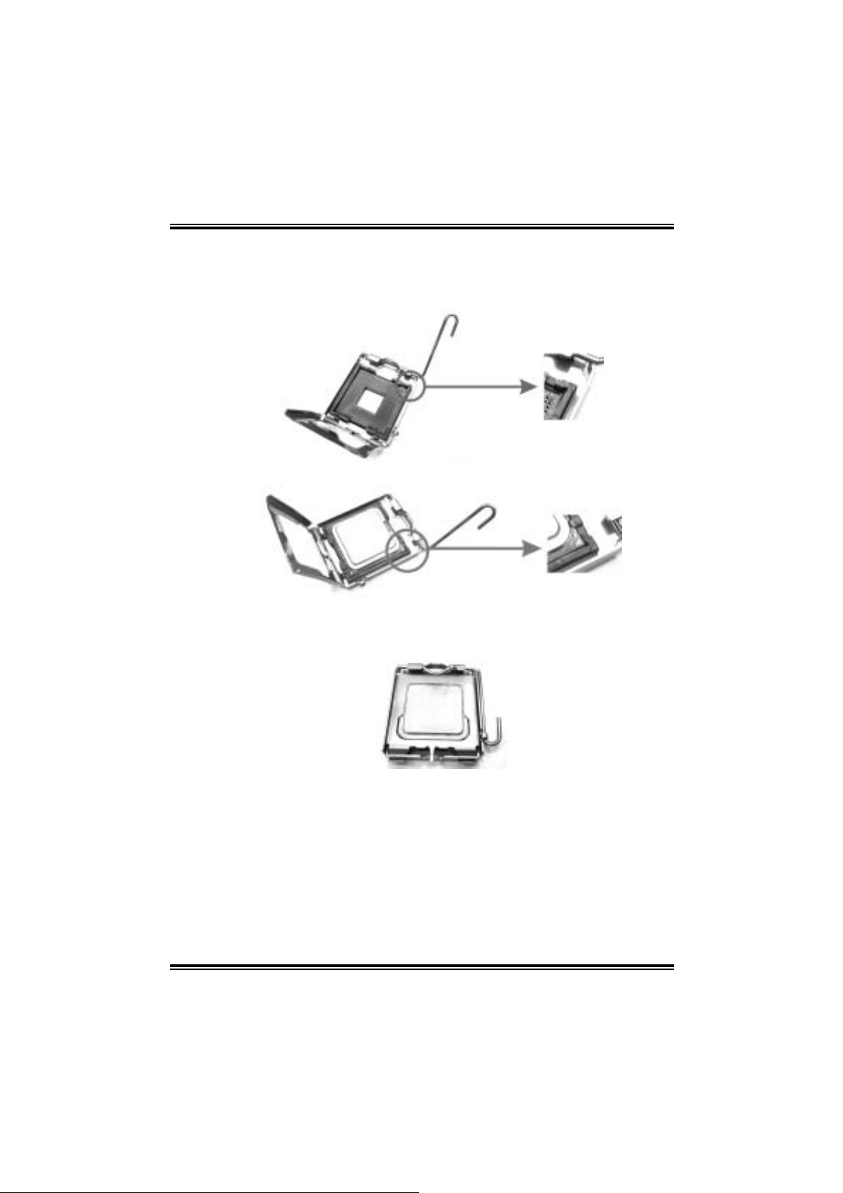
915GV- M7 DD R 2
Step 2: Look for the triangular cut edge on socket, and the golden dot on
CPU should point forwards this triangular cut edge. The CPU will
fit only in the correct orientation.
Step 2-1:
Step 2-2:
Step 3: Hold the CPU down firmly, and then lower the lever to locked
position to complete th e installation.
Step 4: Put the CPU Fan and heatsi nk assembl y on the CPU and buckle i t
on the retention frame. Connect the CPU FAN power cable into
the JCFAN1. This completes the installation.
7
Page 10
915GV- M7 DD R 2
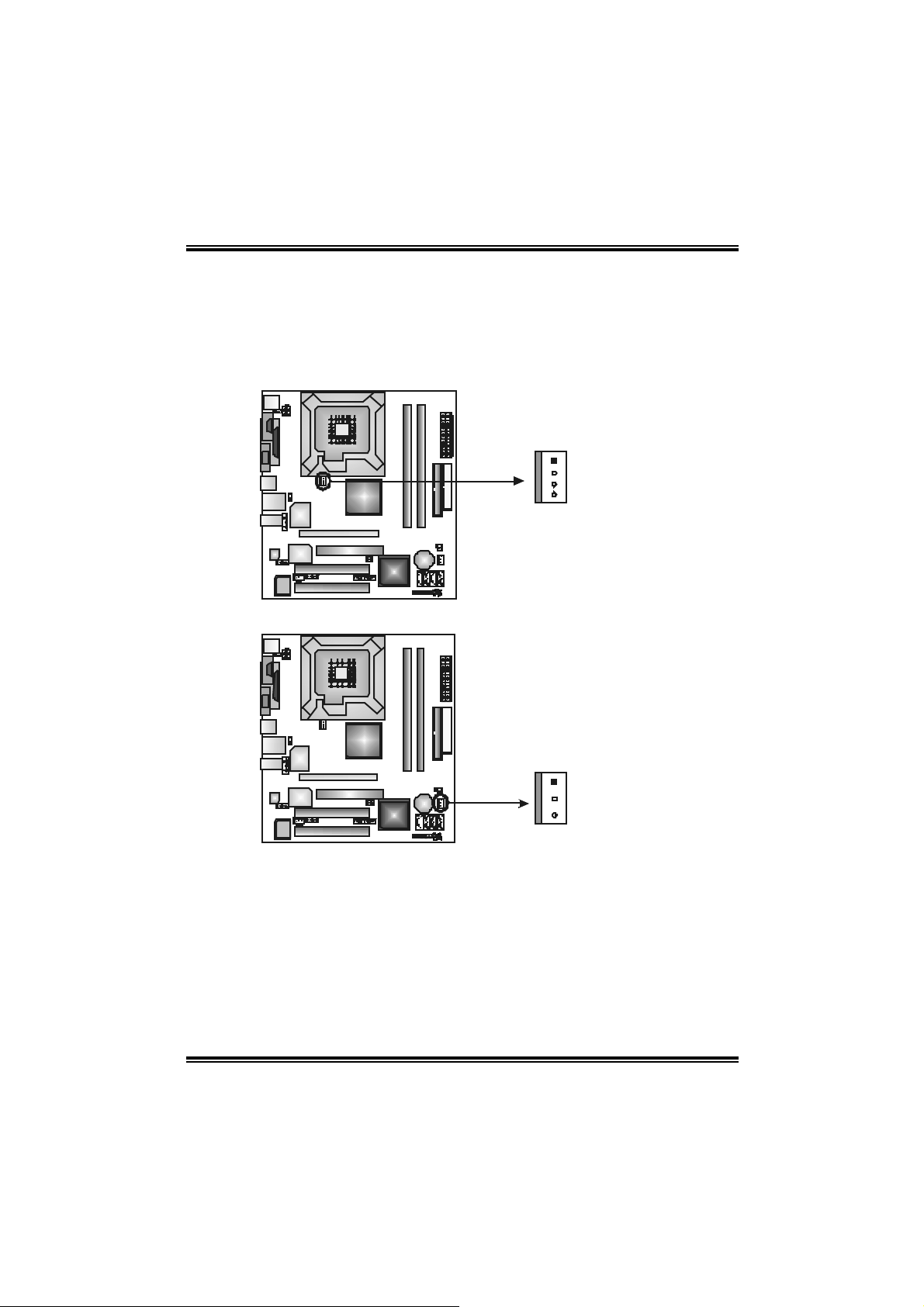
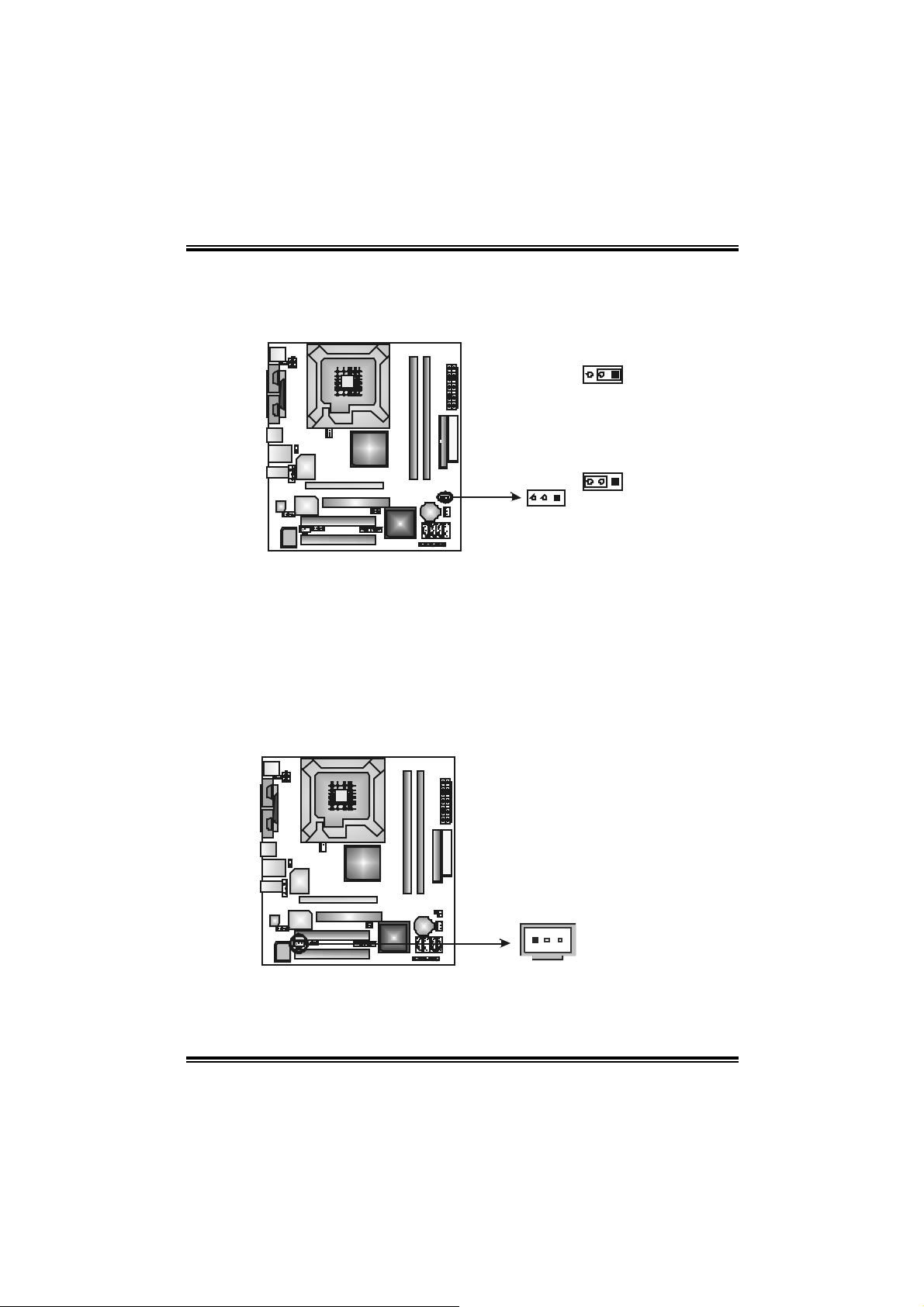
2.2 FAN HEADERS
These fan headers support cooling-fans built in the computer. T he fan
cable and connector may be different according to the fan m anufacturer.
Connect the fan cable to the connector while m atching the black wire to
pin#1.
JCFAN1: CPU Fa n Header
Pin
1
4
Assignment
1 Ground
2 Power
3 FAN RPM rate
sense
4 Smart Fan
Control
JSF AN1 : Syst em F an H ead er
Assignment
Pin
1 Ground
2 +12V
3 FAN RPM rate
sense
1
3
Note:
Th e JCFAN1 reserves system cooling fan with Smart Fan Cont rol utility. It support s 4-pin
head connector. When connecti ng with wires onto c onnectors, please note that the r ed
wire is the positive and should be connected to pin#2, and the bl ac k wire is Ground and
shoul d be connected to GND.
8
Page 11
915GV- M7 DD R 2
_
_
A
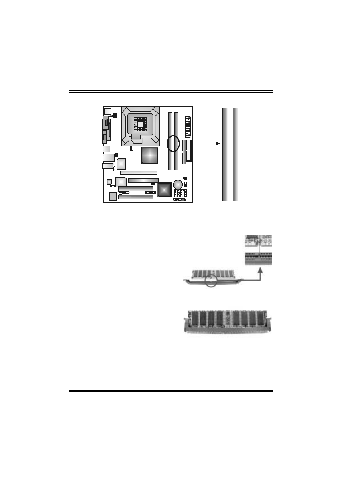
2.3 INSTALLING SYSTEM MEMORY
DDR2
1
1. Unlock a DIMM slot by pressing the retaini ng clips outward. Align a
DIMM on the slot such that the notch on the DIMM matches the break
on the Slot.
DDR2
B1
2. Insert the DIMM vertically and firmly into the slot until the retaining
chip snap back in place and the DIM M is properly seated.
9
Page 12

915GV- M7 DD R 2
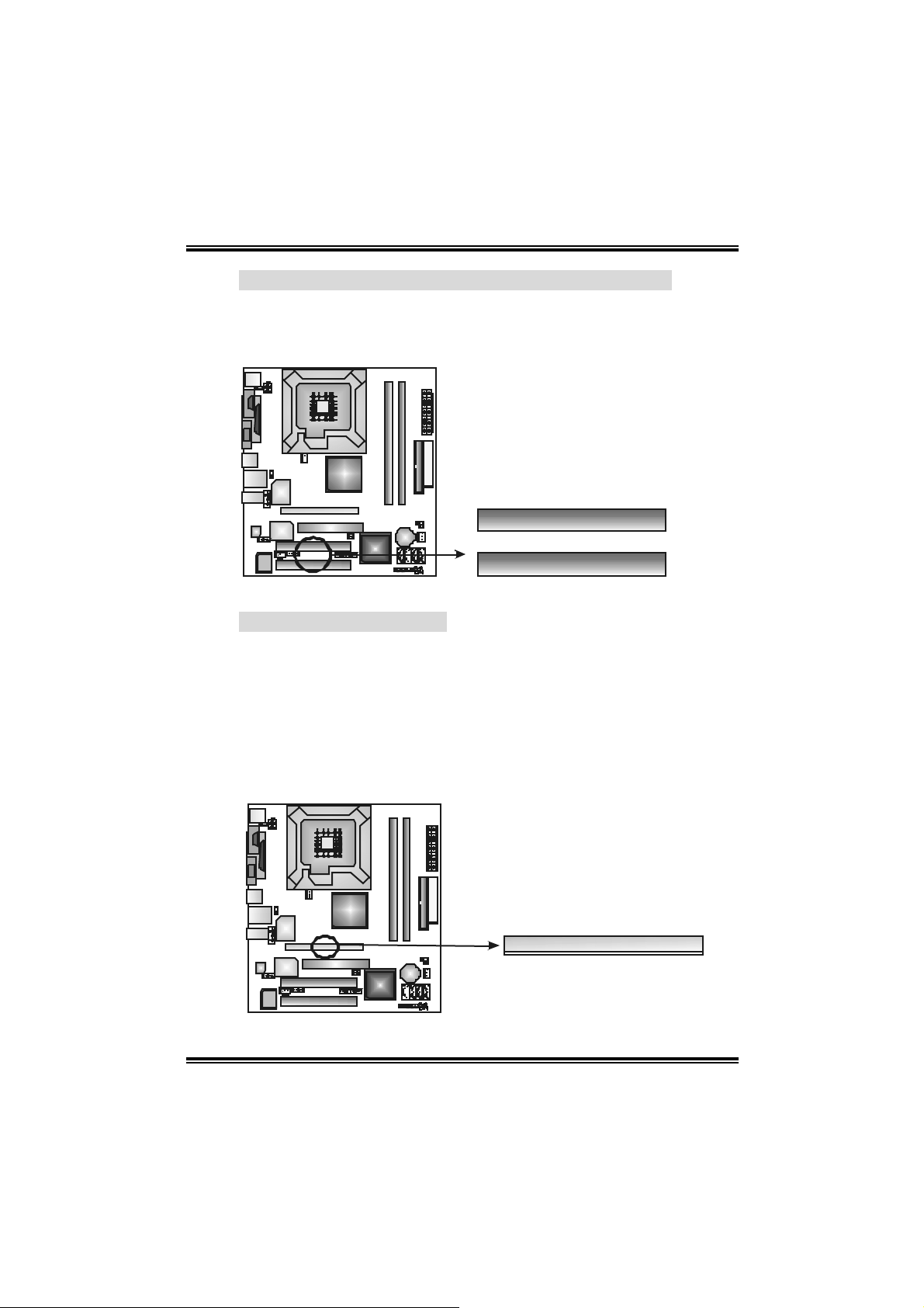
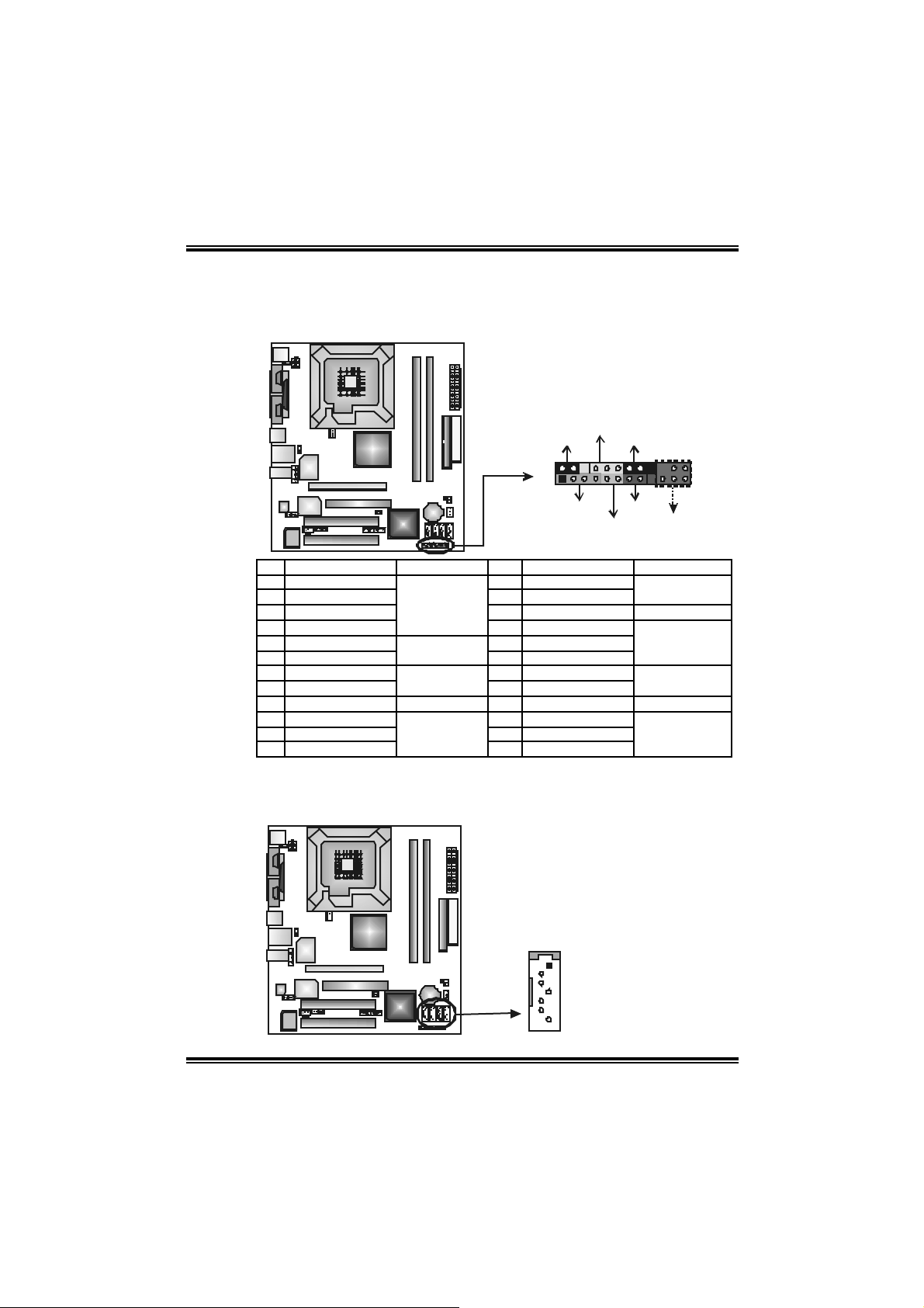
2.4 CONNECTO RS AND SLOTS
FDD1: Floppy Disk Connector
The motherboard provides a standard floppy disk connector that
s uppor t s 360 K, 720K, 1.2 M, 1. 4 4 M a nd 2. 8 8 M f lo ppy d is k types.
This connector supports the provided floppy drive ribbon cables.
12
33
IDE1: Hard Disk Connector
The motherboard has a 32-bit Enhanced PCI IDE Controller that
provides PIO Mode 0~4, Bus Master, and Ul tra DMA 33/66/100
functionality.
The IDE connectors can connect a master and a slave drive, so you
can connect up to two hard disk drives. The fi rst hard drive should
al ways be con nected to IDE1.
34
21
40
39
10
Page 13
915GV- M7 DD R 2
PCI1~PCI2: Pe riphera l Component Interconnect Slots
This motherboard is equipped with 2 standard PCI slots. PCI stands
for Peri pheral Component Interconnect, and it i s a bus standard for
expansi on cards. T his PCI slot is designated as 32 bits.
PCI1
PCI2
PCI-EX: PCI-Extreme Slot
- PCI-Extreme sl ot is a special design for PCI-Express
interface graphic cards.
- PCI-Extreme sl ot is compliant with PCI-Express 1.0a
specifi cation.
- PCI-Extreme sl ot is compatibl e with PCI-E x4 and PCI-E x1
expansi on card.
- The bandwidth of data transfer is up to 1GB/s per direction,
and for an ag gr egate of 2G B/s i n t otal.
11
Page 14

915GV- M7 DD R 2
XGP1: Xtreme Gr aphics Port Slot
This XGP (Extreme Graphics Port) slot is a special design that only
supports compatible AGP VGA cards.
To install the system with an add-on AGP VGA card, please make
sure to install the driver of add-on AGP VGA card before onboard
VGA dr iver i nstallat i on. If the on bo ar d VG A dr iver has a lready bee n
installed before you install the add-on AGP VGA card, the system
will automatically set the onboard VGA as the primary graphics
adapter.
For the onboard VGA driver can’t be removed com pletely, and to
solve thi s problem, please follow the steps bel ow,
1. Disable onboard VGA utility under the operating system, and
reboot PC. After PC restarts, the system will automat ically set
the AGP V GA car d as the graphics a dap ter .
2. Or, re-i nstall your operating system to ensure the AGP VGA
card function can be used.
Note:
Plea se go to “ht tp://www.bio sta r.com .tw” fo r more detail ed
information about XGP compatible A GP c ard s.
12
Page 15
915GV- M7 DD R 2
CHAPTER 3: HEADERS & JUMPERS SE TUP
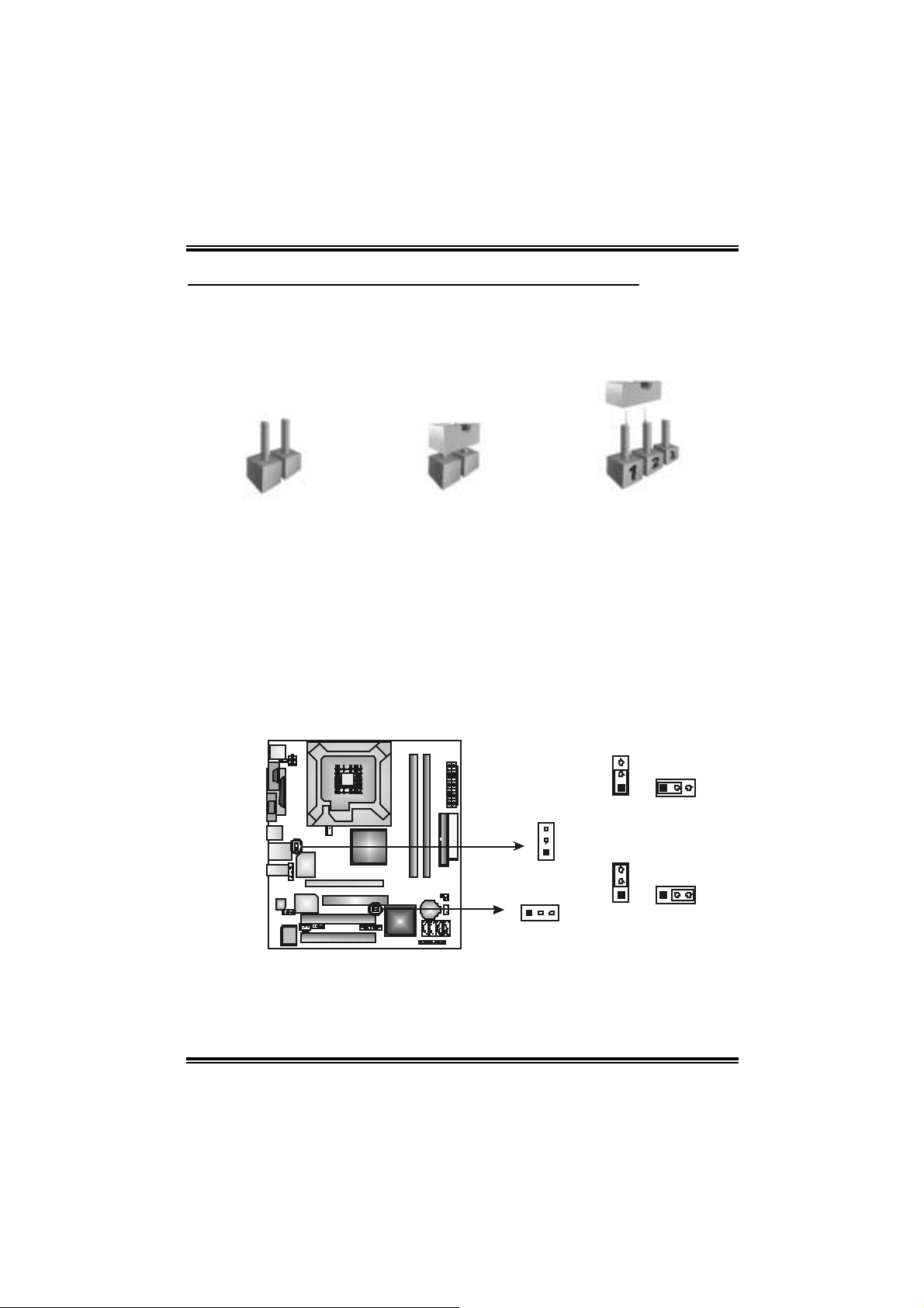
3.1 HOW TO SETUP JUMPERS
The illustration shows how to set up jumpers. When the jum per cap is
placed on pins, the j umper is “close”, if not, that means the jumper is
“open”.
Pin opened Pin closed Pin1-2 closed
3.2 DETAIL SETTINGS
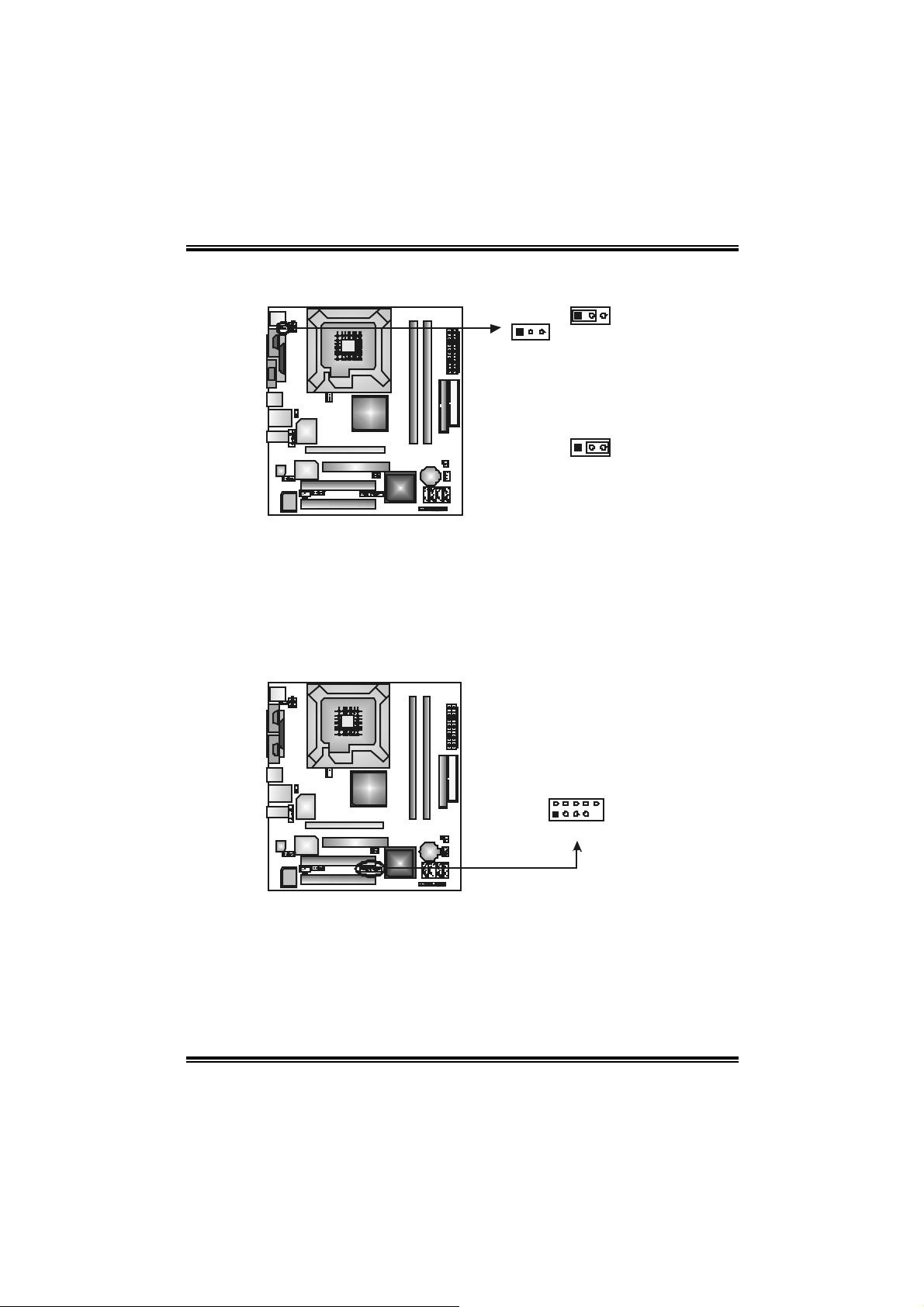
JUSBV1/JUS BV3_1: Power Source Hea d ers for USB P o rts
Pin 1-2 Cl o se:
JU SBV1 : +5V for U SB ports at back panel (JRJ 45USB1/JUSB2).
JU SBV3_1 : +5V for U SB ports at f ront panel (JUSB3/JUSB4).
Pin 2-3 Cl o se:
JU SBV1 : USB ports at back panel (JRJ 45USB1/JUSB2) are powered by
+5V st andby voltage.
JU SBV3_1 : U SB ports at f ront panel (JU SB3/JUSB4) are powered by +5V
standb y voltage.
3
1
JUSBV1
JUSBV3_1
13
Pin 1-2 Close (default)
3
1
3
1
Pin 2-3 Close
Note:
In order to support this function “Power-On system via U SB device,” “JUSBV1/
JUSBV3_1” jumper cap should be plac ed on Pin 2-3 individuall y.
13
31
31
Page 16
915GV- M7 DD R 2
JK BV1 : P o wer So urce H ea der fo r PS/2 Key b o a rd an d Mous e
31
Pin 1-2 Close
13
Note:
In order to support this function “Power-on s ystem via keyboar d and mouse”, “JKBV1”
jumper cap should be plac ed on Pin 2-3.
JUSB3/ JUSB 4: Front USB Headers
This mot herboard provides 2 USB 2.0 headers, which allows user t o connect
additional U SB cable on the PC front panel, and also can be connected wit h
internal U SB devices, like USB c ard reader.
(default)
+5V for PS/2 keyboard and
mouse.
31
Pin 2-3 Close
PS/2 keyboard and mouse
are powered by +5V standby
voltage.
Pin
1 +5V (fused)
2 +5V (fused)
3 USB-
JUSB4JUSB3
2
10
1
9
4 USB5 USB+
6 USB+
7 Ground
8 Ground
9 Key
10
Assignment
NC
14
Page 17
915GV- M7 DD R 2
JAT XPWR1 : AT X Power Con necto r
This connector allows user t o connect 24-pin power connector on the ATX
power supply .
Pin Assignment
1 +3.3V
2 +3.3V
3 Ground
4 +5V
5 Ground
12 24
113
JAT XPWR2 : AT X Power Con necto r
By c onnecting this connector, it will provide +12V to C PU power circ uit.
2
4
1
3
6 +5V
7 Ground
8 PW_OK
9 Standby
Voltage +5V
10 +12V
11 +12V
12 2 x 12 Detect
13 +3.3V
14 -12V
15 Ground
16 PS_ON
17 Ground
18 Ground
19 Ground
20 -5V
21 +5V
22 +5V
23 +5V
24 Ground
Pin
Assignment
1 +12V
2 +12V
3 Ground
4 Ground
15
Page 18
915GV- M7 DD R 2
JCDIN1 : CD-ROM Au d i o -in Con nector
This connector allows user to connect t he audio source f rom the v ariety devic es,
like CD-R OM, DVD-ROM, PCI sound card, PCI TV turner card etc..
Assignment
Pin
1 Left channel input
2 Ground
3 Ground
4
Right channel input
14
JAUDIO 2 : Fron t Panel Au di o Header
This header allows us er t o connect the f ront audio output cable with the PC front
panel. It will dis able the output on back panel audio c onnectors.
Pin Assignment
1 Mic in/center
2 Ground
3 Mic power/Bass
4 Audio power
5 Right line out/
6 Right line out/
7 Reserved
8 Key
13
14
2
9 Left line out/
10 Left line out/
11 Right line in/
1
12 Right line in/
13 Left line in/
14 Left line in/
Speaker out Right
Speaker out Right
Speaker out Left
Speaker out Left
Rear speaker Right
Rear speaker Right
Rear speaker Left
Rear speaker Left
16
Page 19
915GV- M7 DD R 2
_
(op
)
JPANEL1: Front Panel Header
This 24-pin connector includes Power-on, Reset, HDD LED, Power LED, Sleep
butt on, speaker and I rDA Connection. I t allows user to connect the PC case’s
front panel switch fun ctions.
PWR
LED
SLP
2
123
SPK
Pin Assignment Functio n Pin Assignment Function
1 +5V 2 Sleep control
3 N/A 4 Ground
5 N/A 6 N/A N/A
7 Speaker
9 HDD LE D (+) 10 P ower LED (+)
11 HDD LED (-)
13 Ground 14 Power button
15 Reset control
17 N/A 18 N/A
19 N/A 20 Key
21 +5V 22 Ground
23 IRTX
Speaker
Connector
Hard drive LED
Reset button
IrDA Connector
(optional)
8 Power L ED (+)
12 Powe r LED (-)
16 Ground
24 IRRX
SATA1~SAT A4: Serial ATA Conn ectors
The motherboard has a PCI to SATA Cont roller wit h 4 channels SATA interf ace,
it satisfies the SATA 2.0 spec and with transfer rate of 3Gb/s.
SATA4
SATA3
SATA2
SATA1
1
4
On/Off
-
++
-
+
RST
HLED
Sleep button
Powe r LED
Power-on button
IrDA Connector
(optional)
Pin
1 Ground
2 TX+
3 TX4 Ground
5 RX6 RX+
7 Ground
IR
Assignment
24
tional
7
17
Page 20
915GV- M7 DD R 2
JCMOS1: Cl ea r C MO S H ea der
By plac ing the jum per on pin2-3, it allows user to rest ore the BIOS saf e setting
and the CMOS data, please carefully f ollow t he proc edures to avoid damaging
the m otherboard.
13
Pin 1-2 Close
Normal Operation (default).
13
13
※ Clea r CMO S P ro ced ures :
1. R em ov e AC power line.
2. Set the jumper to “Pin 2-3 Close”.
3. Wait for fi ve se co n ds.
4. Set the jumper to “Pin 1-2 Close”.
5. Power on the AC.
6. R es et y our desired pas s word or c lear t he CMOS data.
Pin 2-3 Close
Clear CMOS data.
JSPDIF_OUT1: Digital Audio-out Con nector
This connector allows user t o connect the PCI bracket SPDIF output header.
Assignment
Pin
1 +5V
2 SPDIF_OUT
3 Ground
13
18
Page 21

915GV- M7 DD R 2
JCI1: Chassis Open He ader
This connector allows sy stem to monitor PC cas e open status. If the s ignal has
been triggered, it will rec ord to the CMOS and show the message on next
boot-up.
Assignment
Pin
1 Case open signal
2 Ground
21
JAUX1: AUX Au d i o -in Conn ector
Assignment
Pin
1 Left channel input
2 Ground
3 Ground
Right channel input
4
14
19
Page 22

915GV- M7 DD R 2
CHAPTER 4: USEFUL HELP
4.1 AWARD BIOS BEEP CODE
Beep Sound Meanin g
One long beep f ollowed by t wo s hort
beeps
High-low siren sound CPU overheated
One Short beep when system boot-up No error found during POST
Long beeps every ot her second No DRAM detected or inst all
4.2 EXTRA INF ORMATION
A. BIOS Update
After you fail to up d ate B IOS or BIOS i s i n vaded b y virus, the
Boot-Block function wi ll help to restore BIOS. If the following message
is shown after boot-up the system, it means the BIOS contents are
corrupted.
Video card not f ound or video c ard
mem ory bad
Sys t em will shut down automat ically
In this Case, please follow the procedure below to restore the BIOS:
1. Mak e a bootab le fl op py d is k.
2. Download the Flash Utility “AWDFLASH.exe” from the Biostar
website: www.bi o star.com.tw
3. Confi rm m otherboard model and download the respectively
BIOS from Biostar website.
4. Copy “AWDFLASH.exe” and respecti vely BIOS into floppy disk.
5. Insert the bootable disk into floppy drive and press Enter.
6. System will boo-up to DOS prom pt.
7. Type “Awd flash xxxx.bf / sn/p y/ r” i n DOS prompt.
8. System will update B IOS automatically and re sta rt.
9. The BIOS has been recovered a nd will work properl y.
20
Page 23

915GV- M7 DD R 2
B. CPU Overheated
If the system shutdown automatically after power on system for
seconds, that means the CPU protecti on function has been activated.
When the CPU is over heated, the motherboard will shutdown
automatically to avoid a damage of the CPU, and the system may not
power on again.
In this case, please double check:
1. The CPU cooler surface is placed evenly with the CPU surface.
2. CPU fan is rotated normally.
3. CPU fan speed is ful fil ling with the CPU speed.
After confirmed, please follow steps below to rel ief the CPU protecti on
function.
1. Remove the power cord from power supply for seconds.
2. Wait for seconds.
3. Plug in the power cord and boot up the system.
Or you can:
1. Clear the CMOS data.
(See “Close CMOS Header: JCM OS1” section)
2. Wait for seconds.
3. Power on the syst em again.
21
Page 24

915GV- M7 DD R 2
e
4.3 TROUBLESH OOTING
Problem Solution
1. N o power to the system at all
Power light don’t illuminat e, fan
inside power s upply does not turn
on.
2. I ndic at or light on keyboard does
not t urn on.
Sys t em inoperat iv e. Keyboard lights
are on, power indic at or lights are lit,
and hard driv e is spinning.
Sys t em does not boot from hard disk
drive, c an be booted f rom optical drive.
Sys t em only boots from optical drive.
Hard disk can be read and applications
can be used but booting from hard dis k
is imposs ible.
Screen m essage say s “Invalid
Conf igurat ion” or “CMOS Failure.”
Cannot boot sys t em aft er inst alling
sec ond hard drive.
1. Make s ure power c able is
sec urely plugged in.
2. Replace cable.
3. Contact technical support.
Us ing even pres s ure on bot h ends of
the DIMM, press down firm ly until the
module s naps int o place.
1. C hec k cable running from disk to
disk controller board. Make sure
both ends are s ec urely plugged
i n; chec k t h e driv e t y p e in t h e
standard CMOS setup.
2. Bac k ing up the hard drive is
ext rem ely im port ant. All hard
disk s are c apable of breaking
down at any t ime.
1. Bac k up data and applications
files.
2. R ef orm at t he hard drive.
Re-ins t all applicat ions and data
using backup disks.
Rev iew sys t em’s equipment. Make s ur
correc t inf ormat ion is in setup.
1. Set m aster/slave jum pers
correctly.
2. R un SETUP program and s elect
correc t driv e types. Call the driv e
manufacturers for co mpatibilit y
with other drives.
22
Page 25

915GV- M7 DD R 2
CHAPTER 5: WARPSPEEDER™
5.1 INTRODUCTION
[WarpSpeeder™], a new powerful control utility, features three
user-friendly functions including Overclock Manager, Overvoltage
Manager, and Hardware Monitor.
With the Overclock Manager, users can easily adjust the frequency they
prefer or they can get the best CPU performance with just one click. The
Overvol tage Manager, on the other hand, helps to power up CPU core
vol tage an d Me mor y v olt a ge. The co o l H ardw are Mo nit or s mar tly in d icates
the temperatures, vol tage and CPU fan speed as well as the chipset
information. Also, in the About panel, you can get detail descriptions about
BIOS model and chipsets. In addition, the frequency status of CPU,
memory, AGP and PCI along with the CPU speed are synchronically
s how n on our ma i n p an el .
Moreover, to protect users' computer systems i f the setting is not
appropriate when testing and results in system fail or hang,
[WarpSpeeder™] technology assures the system stability by autom atically
rebooting the computer and then restart to a speed that is either the
original system speed or a suitable one.
5.2 SYSTEM REQUIREMENT
OS Support: Windows 98 SE, Windows M e, Windows 2000, Windows XP
DirectX: DirectX 8.1 or above. (The Windows XP operati ng system
incl udes DirectX 8.1. If you use Windows XP, you do not need to install
Dir ec tX 8.1.)
23
Page 26

915GV- M7 DD R 2
5.3 INSTALLATION
1. Execute the setup executi on file, and then the following dialog will pop
up. Please click “Next” button and foll ow the default procedure to
install.
2. When you see the foll owi ng dialog in setup procedure, it means setup
is completed. If the “Launch the WarpSpeeder Tray Utility” checkbox
is chec ked, th e Tra y Ico n utilit y and [WarpSpeede r™ ] util ity will b e
automatically and immediately launched after you click “Fini sh”
button.
Usage:
The following figures are j ust only for reference, the screen printed in
this u ser manual will ch an ge ac c ord ing to your m otherboard on ha nd.
24
Page 27

915GV- M7 DD R 2
5.4 [WARPSPEEDER™] INCLUDES 1 TRAY ICON AND 5 PANELS
1. Tray Icon:
Whenever the Tray Icon utility is launched, it will di splay a little tray
icon on the ri ght si de of Windows Taskbar.
This utility is responsi ble for conveniently invoking [WarpSpeeder™]
Utility. You can use the mouse by clicki ng the left button in order to
invoke [WarpSpeeder™] directl y from the little tray icon or you can
right-click the little tray icon to pop up a popup menu as following
figure. The “Launch Utility” item in the popup menu has the same
fun c tion a s m ou se left-click on tray ic on and “Exit” item will cl ose
T ray Icon utility if selected.
25
Page 28

915GV- M7 DD R 2
2. Main Panel
If y ou click the t ray icon , [Wa rpS pe eder™ ] utility will b e in voked.
Please refer to the following figure; th e utility’s first window you will
see is Main Panel.
Main Panel contains fe atures as follows:
a. Display the CPU Spe ed, CPU extern al clock, Memory cl ock, A GP clock,
and PCI clock information.
b. Contains About, Voltage, Overclock, and Hardware Monitor Buttons for
invoking respecti ve panels.
c. W ith a user- f r ie nd ly Status An im at io n, it c an represent 3 over cl oc k
percentage stages:
Man walking→overclock percentage from 100% ~ 110 %
Panther running→overclock percentage from 110% ~ 120%
Ca r rac ing→overclock percentage from 120% ~ above
26
Page 29

915GV- M7 DD R 2
3. Vol ta ge Panel
Click the Voltage button in Main Pa nel , the butt on will be hig hlighte d
and the Vol tage Panel will sl ide out t o up as the following fig ure .
In this panel, you can decide to increase CPU core voltage and
Memory voltag e or not. The default se tting is “No”. If yo u want to get
the best performance of overclocking, we recommend you click the
opti on “Yes”.
27
Page 30

915GV- M7 DD R 2
4. Over clock Panel
Click the Overclock button in Main Panel, the bu tton will be
highlighted and the Overclock Panel will slide out to left as the
fol l owi ng f igur e.
Overclock Panel cont ains the these fea tures:
a. “–3MHz button”, “-1MHz button”, “+1MHz button”, and “+3MHz button”:
provide user the abili ty to do real-time overclock adjustment.
Warning:
Manually overclock is pot entially dangerous, especially when t he
overclocking perc entage is over 110 %. We st rongly rec ommend you
verify every speed you ov erc lock by c lic k the Verify butt on. Or, you c an
just click Aut o overc lock button and let [W arpSpeeder™] autom atically
gets the best result for y ou.
b. “Recovery Dialog button”: Pop up the following dialog. Let user select
a restoring way if system need to do a fail-safe reboot.
28
Page 31

915GV- M7 DD R 2
c. “Auto-overclock button”: User can click this button and
[Wa rpS peede r™ ] will se t the be st and stable performance and
frequency automatically. [WarpSpeeder™] utili ty will execute a
se ries o f testing u ntil system fail. Then system will do fail-saf e
reboot by using Watchdog function. After reboot, the
[WarpSpeeder™] utility will restore to the hardware defaul t
setting or load the verified best and stable frequency according
to the Recovery Dialog’s setting.
d. “Verify button”: User can click this button and [WarpSpeeder™]
will proceed a testing for current frequency. If the testing is ok,
then the current fre q uency will be saved into system registry. If
the testing fail, system will do a fail-safe rebooting. After reboot,
the [WarpSpe eder™ ] utility will re sto re to the hard ware de fault
setting or load the verified best and stable frequency according
to the Recovery Dialog’s setting.
Note:
Becaus e the t esting programs, invok ed in Auto-overclock and Verify,
include D irectDraw, D irect3D and DirectShow t ests, the DirectX 8.1 or
newer runtime library is required. And pleas e make sure y our display
card’s color depth is High color (16 bit ) or True c olor (24/32 bit) that is
required for Direct3D rendering.
5. Hardware Monitor Panel
Click the Ha rdwa re Mo nitor button in Main Pane l, the bu tton will be
highlighted and the Hardware Monitor panel will slide out to left as
the fo l lowing figur e.
In this panel, you can get the real-time status information of your
system. The info rmation will be refreshed every 1 second.
29
Page 32

915GV- M7 DD R 2
6. About Panel
Click the “about” button in M ain Panel, the button will be highlighted
and th e A b out Pane l will s l id e out t o up as the fo l low in g f igur e.
In this panel, you can get model name and detail information in hints
of all the chipset that are related to overclocking. You can also get
the mainboard’s BIOS model and the Version number of
[WarpSpeeder™] utility.
30
Page 33

915GV- M7 DD R 2
Note:
Because the overclock, overvoltage, and hardware monitor features
are controlled by several separate chipset, [WarpSpeeder™] divide
these features to separate panels. If one chipset i s not on board, the
cor r elat ive button in Main panel will be disabled, but will not interfere
other panels’ functions. This property can make [WarpSpeeder™]
utility more robust.
31
Page 34

915GV-M7 DDR2
BIOS SETUP
BIOS Setup ......................................................................1
1 Main Menu .................................................................................................... 3
2 Standard CMOS Features.............................................................................. 6
3 Advanced BIOS Features..............................................................................9
4 Advanced Chipset Features......................................................................... 14
5 Integrated Peripherals..................................................................................17
6 Power Management Setup...........................................................................22
7 PnP/PCI Configurations ..............................................................................27
8 PC Health Status .........................................................................................29
9 Frequency/ Voltage Control ........................................................................30
i
Page 35

915GV-M7 DDR2
BIOS SETUP
BIOS Setup
Introduction
This manual discussed Award™ Setup program built into the ROM BIOS. The Setup
program allows users to modify the basic system configuration. This special information is
then stored in battery-backed RAM so that it retains the Setup information when the power
is turned off.
The Award BIOS™ installed in your computer system’s ROM (Read Only Memory) is a
custom version of an industry standard BIOS. This means that it supports Intel Pentium
processor input/output system. The BIOS provides critical low-level support for standard
devices such as disk drives and serial and parallel ports.
Adding important has customized the Award BIOS™, but nonstandard, features such as
virus and password protection as well as special support for detailed fine-tuning of the
chipset controlling the entire system.
The rest of this manual is intended to guide you through the process of configuring your
system using Setup.
Plug and Play Support
These AWARD BIOS supports the Plug and Play Version 1.0A specification. ESCD
(Extended System Configuration Data) write is supported.
EPA Green PC Support
This AWARD BIOS supports Version 1.03 of the EPA Green PC specification.
APM Support
These AWARD BIOS supports Version 1.1&1.2 of the Advanced Power Management
(APM) specification. Power management features are implemented via the System
Management Interrupt (SMI). Sleep and Suspend power management modes are supported.
Power to the hard disk drives and video monitors can be managed by this AWARD BIOS.
ACPI Support
Award ACPI BIOS support Version 1.0 of Advanced Configuration and Power interface
specification (ACPI). It provides ASL code for power management and device
configuration capabilities as defined in the ACPI specification, developed by Microsoft,
Intel and Toshiba.
®
4
1
Page 36

915GV-M7 DDR2
BIOS SETUP
PCI Bus Support
This AWARD BIOS also supports Version 2.1 of the Intel PCI (Peripheral Component
Interconnect) local bus specification.
DRAM Support
DDR2 SDRAM (Double Data Rate Two Synchronous DRAM) are supported.
Supported CPUs
This AWARD BIOS supports the Intel CPU.
Using Setup
In general, you use the arrow keys to highlight items, press <Enter> to select, use the
<PgUp> and <PgDn> keys to change entries, press <F1> for help and press <Esc> to quit.
The following table provides more detail about how to navigate in the Setup program by
using the keyboard.
Keystroke Function
Up arrow Move to previous item
Down arrow Move to next item
Left arrow Move to the item on the left (menu bar)
Right arrow Move to the item on the right (menu bar)
Move Enter Move to the item you desired
PgUp key Increase the numeric value or make changes
PgDn key Decrease the numeric value or make changes
+ Key Increase the numeric value or make changes
- Key Decrease the numeric value or make changes
Esc key Main Menu – Quit and not save changes into CMOS
F1 key General help on Setup navigation keys
F5 key Load previous values from CMOS
F7 key Load the optimized defaults
F10 key Save all the CMOS changes and exit
Status Page Setup Menu and Option Page Setup Menu – Exit
Current page and return to Main Menu
2
Page 37

1 Main Menu
Once you enter Award BIOS™ CMOS Setup Utility, the Main Menu will appear on the
screen. The Main Menu allows you to select from several setup functions. Use the arrow
keys to select among the items and press <Enter> to accept and enter the sub-menu.
!! WARNING !!
The information about BIOS defaults on manual (Figure
1,2,3,4,5,6,7,8,9) is just for reference, please refer to the BIOS
installed on board, for update information.
Figure 1. Main Menu
915GV-M7 DDR2
BIOS SETUP
Standard CMOS Features
This submenu contains industry standard configurable options.
Advanced BIOS Features
This submenu allows you to configure enhanced features of the BIOS.
Advanced Chipset Features
This submenu allows you to configure special chipset features.
3
Page 38

915GV-M7 DDR2
BIOS SETUP
Integrated Peripherals
This submenu allows you to configure certain IDE hard drive options and Programmed
Input/ Output features.
Power Management Setup
This submenu allows you to configure the power management features.
PnP/PCI Configurations
This submenu allows you to configure certain “Plug and Play” and PCI options.
PC Health Status
This submenu allows you to monitor the hardware of your system.
Frequency/ Voltage Control
This submenu allows you to change CPU Vcore Voltage and CPU/PCI clock. (However,
this function is strongly recommended not to use. Not properly change the voltage
and clock may cause the CPU or M/B damage!)
Load Optimized Defaults
This selection allows you to reload the BIOS when the system is having problems
particularly with the boot sequence. These configurations are factory settings optimized
for this system. A confirmation message will be displayed before defaults are set.
Set Supervisor Password
Setting the supervisor password will prohibit everyone except the supervisor from making
changes using the CMOS Setup Utility. You will be prompted with to enter a password.
4
Page 39

915GV-M7 DDR2
BIOS SETUP
Set User Password
If the Supervisor Password is not set, then the User Password will function in the same
way as the Supervisor Password. If the Supervisor Password is set and the User
Password is set, the “User” will only be able to view configurations but will not be able to
change them.
Save & Exit Setup
Save all configuration changes to CMOS(memory) and exit setup. Confirmation message
will be displayed before proceeding.
Exit Without Saving
Abandon all changes made during the current session and exit setup. Confirmation
message will be displayed before proceeding.
Upgrade BIOS
This submenu allows you to upgrade bios.
5
Page 40

915GV-M7 DDR2
BIOS SETUP
2 Standard CMOS Features
The items in Standard CMOS Setup Menu are divided into 10 categories. Each category
includes no, one or more than one setup items. Use the arrow keys to highlight the item
and then use the<PgUp> or <PgDn> keys to select the value you want in each item.
Figure 2. Standard CMOS Setup
6
Page 41

915GV-M7 DDR2
BIOS SETUP
Main Menu Selections
This table shows the selections that you can make on the Main Menu.
Item Options Description
Date mm : dd : yy Set the system date. Note
Time hh : mm : ss Set the system internal
IDE Primary Master Options are in its sub
menu.
IDE Primary Slave Options are in its sub
IDE Secondary Master Options are in its sub
IDE Secondary Slave Options are in its sub
Drive A
Drive B
Video EGA/VGA
menu.
menu.
menu.
360K, 5.25 in
1.2M, 5.25 in
720K, 3.5 in
1.44M, 3.5 in
2.88M, 3.5 in
None
CGA 40
CGA 80
MONO
that the ‘Day’ automatically
changes when you set the
date.
clock.
Press <Enter> to enter the
sub menu of detailed
options
Press <Enter> to enter the
sub menu of detailed
options.
Press <Enter> to enter the
sub menu of detailed
options.
Press <Enter> to enter the
sub menu of detailed
options.
Select the type of floppy
disk drive installed in your
system.
Select the default video
device.
7
Page 42

915GV-M7 DDR2
BIOS SETUP
Item Options Description
Halt On All Errors
No Errors
All, but Keyboard
All, but Diskette
All, but Disk/ Key
Base Memory N/A Displays the amount of
Extended Memory N/A Displays the amount of
Total Memory N/A Displays the total memory
Select the situation in which
you want the BIOS to stop
the POST process and
notify you.
conventional memory
detected during boot up.
extended memory detected
during boot up.
available in the system.
8
Page 43

915GV-M7 DDR2
BIOS SETUP
3 Advanced BIOS Features
Figure 3. Advanced BIOS Setup
CPU FEATURE
Delay Prior to Thermal
Set this item to enable the CPU Thermal function to engage after the
specified time.
The Choices: 4, 8, 16 (default), 32.
Thermal Management
Allow you to choose the thermal management method of your monitor.
The Choices: Thermal Monitor 1 (default), Thermal Monitor2.
Notes: The choices will be different according to your CPU features.
9
Page 44

915GV-M7 DDR2
BIOS SETUP
TM2 Bus Ratio
Represents the frequency. Bus ratio of the throttled performance state that will
be initiated when the on-die sensor goes from not hot to hot.
The Choices: 0X (default).
TM2 Bus VID
Represents the voltage of the throttled performance state that will be initiated
when the on-die sensor goes from not hot to hot.
The Choices: 0.8375 (default).
Limit CPU ID Max Val
Set limit CPU ID maximum vale to 3, it should be disabled for Win XP.
The Choices: Disabled (default), Enabled.
Execute Disable Bit
The Choices: Enabled (default), Disabled.
HARD DISK BOOT PRIORITY
These BIOS attempt to load the operating system from the device in the sequence
select in these items.
The Choices: Pri. Master, Pri. Slave, Sec. Master, Sec. Slave, USBHDD0, BHDD1,
USBHDD2 and Bootable Add-in Cards.
10
Page 45

915GV-M7 DDR2
BIOS SETUP
BOOT SEQ & FLOPPY SETUP
Virus Warning
First/Second/Third/Boot Other Device
These BIOS attempt to load the operating system from the device in the
sequence selected in these items.
The Choices: Floppy, LS120, HDD-0, SCSI, CDROM, HDD-1, HDD-2,
HDD-3, ZIP100, LAN, HPT370, Disabled, Enabled.
Swap Floppy Drive
For systems with two floppy drives, this option allows you to swap logical
drive assignments.
The Choices: Disabled (default), Enabled.
Boot Up Floppy Seek
Enabling this option will test the floppy drives to determine if they Have 40 or
80 tracks. Disabling this option reduces the time it takes to boot-up.
The Choices: Disabled, Enabled (default)
Report NO FDD for Win95
The Choices: NO (default).
This option allows you to choose the Virus Warning feature that is used to protect
the IDE Hard Disk boot sector. If this function is enabled and an attempt is made to
write to the boot sector, BIOS will display a warning message on the screen and
sound an alarm beep.
Disabled (default) Virus protection is disabled.
Enabled Virus protection is activated.
11
Page 46

915GV-M7 DDR2
BIOS SETUP
CPU L3 Cache
Depending on the CPU/chipset in use, you may be able to increase
memory access time with this option.
Enabled (default) Enable cache.
Disabled Disable cache.
HYPER-THREADING TECHNOLOGY
This option allows you to enable or disabled CPU Hyper-Threading.
Enabled for Windows XP and Linux 2.4.x (OS optimized for Hyper
Threading Technology. Disabled for other OS (OS not optimized for
Hyper Threading Technology.
The Choices: Enabled (default), Disabled.
QUICK POWER ON SELF TEST
Enabling this option will cause an abridged version of the Power On
Self-Test (POST) to execute after you power up the computer.
Disabled Normal POST.
Enabled (default) Enable quick POST.
BOOT UP NUMLOCK STATUS
Selects the NumLock. State after power on.
On (default) Numpad is number keys.
Off Numpad is arrow keys.
GATE A20 OPTION
Select if chipset or keyboard controller should control Gate A20.
Normal A pin in the keyboard controller controls GateA20.
Fast (default) Lets chipset control Gate A20.
TYPEMATIC RATE SETTING
When a key is held down, the keystroke will repeat at a rate determined by
the keyboard controller. When enabled, the typematic rate and typematic
delay can be configured.
The Choices: Disabled (default), Enabled.
TYPEMATIC RATE (CHARS/SEC)
Sets the rate at which a keystroke is repeated when you hold the keydown.
The Choices: 6 (default), 8,10,12,15,20,24,30
TYPEMATIC DELAY (MSEC)
Sets the delay time after the key is held down before it begins to repeat
the keystroke.
The Choices: 250 (default), 500, 750, and 1000.
12
Page 47

915GV-M7 DDR2
SECURITY OPTION
This option will enable only individuals with passwords to bring the system
online and/or to use the CMOS Setup Utility.
System A password is required for the system to boot and is also
required to access the Setup Utility.
Setup (default) A password is required to access the Setup Utilityonly.
This will only apply if passwords are set from the Setup main menu.
APIC MODE
Selecting Enabled enables APIC device mode reporting from the BIOS to
the operating system.
The Choices: Enabled (default), Disabled.
MPS VERSION CONTROL FOR OS
The BIOS supports version 1.1 and 1.4 of the Intel multiprocessor
specification.
Select version supported by the operation system running on this
computer.
The Choices: 1.4 (default), 1.1.
OS SELECT FOR DRAM > 64MB
A choice other than Non-OS2 is only used for OS2 systems with memory
exceeding 64MB.
The Choices: Non-OS2 (default), OS2.
SMALL LOGO (EPA) SHOW
This item allows you to select whether the “Small Logo” shows.
Enabled (default) “Small Logo” shows when system boot up.
Disabled No “Small Logo” shows when system boots up.
SUMMARY SCREEN SHOW
This item allows you to enable/disable the summary screen. Summary
screen means system configuration and PCI device listing.
The choices: Enabled, Disabled (default).
BIOS SETUP
13
Page 48

915GV-M7 DDR2
BIOS SETUP
4 Advanced Chipset Features
This submenu allows you to configure the specific features of the chipset installed on your
system. This chipset manage bus speeds and access to system memory resources, such as
DRAM. It also coordinates communications with the PCI bus. The default settings that came
with your system have been optimized and therefore should not be changed unless you are
suspicious that the settings have been changed incorrectly.
Figure 4. Advanced Chipset Setup
DRAM TIMING SELECTABLE
When synchronous DRAM is installed, the number of clock cycles of CAS
latency depends on the DRAM timing.
The Choices: By SPD (default), Manual.
CAS LATENCY TIME
When synchronous DRAM is installed, the number of clock cycles of CAS
latency depends on the DRAM timing.
The Choices: 3, 2.5, 2, Auto (default).
DRAM RAS# TO CAS# DELAY
This field let you insert a timing delay between the CAS and RAS strobe
signals, used when DRAM is written to, read from, or refreshed. Fast gives
faster performance; and slow gives more stable performance. This field
applies only when synchronous DRAM is installed in the system.
The Choices: 2, 3, 4, 5, Auto (default).
14
Page 49

915GV-M7 DDR2
DRAM RAS# PRECHARGE
If an insufficient number of cycles is allowed for RAS to accumulate its
charge before DRAM refresh, the refresh may be incomplete, and the
DRAM may fail to retain data. Fast gives faster performance; and Slow
gives more stable performance. This field applies only when synchronous
DRAM is installed in the system.
The Choices: 2, 3, 4, 5, Auto (default).
PRECHARGE DELAY (TRAS)
This item controls the number of DRAM clocks to activate the precharge
delay.
The Choices: Auto (default), 4, 5, 6, 7, 8, 9, 10, 11, 12, 13, 14, 15.
SYSTEM MEMORY FREQUENCY
This item allows you to select the Memory Frequency.
The Choices: Auto (default), 333MHz, 400MHz, 533MHz.
SLP_S4# ASSERTION WIDTH
This item sets the minimum assertion width of the SLP-S4# signal to
guarantee the DRAM has been safely power-cycled.
SYSTEM BIOS CACHEABLE
Selecting Enabled allows you caching of the system BIOS ROM at
F0000h~FFFFFh, resulting a better system performance. However, if any
program writes to this memory area, a system error may result.
The Choices: Enabled (default), Disabled.
VIDEO BIOS CACHEABLE
Select Enabled allows caching of the video BIOS, resulting a better
system performance. However, if any program writes to this memory area,
a system error may result.
The Choices: Disabled (default), Enabled.
MEMORY HOLE AT 15M-16M
You can reserve this area of system memory for ISA adapter ROM. When
this area is reserved it cannot be cached. The user information of
peripherals that need to use this area of system memory usually2
discussed their memory requirements.
The Choices: Disabled (default), Enabled.
BIOS SETUP
15
Page 50

915GV-M7 DDR2
VGA Setting
On-Chip Video Memory Size
Select Enabled allows caching of the video BIOS, resulting a better system
performance. However, if any program writes to this memory area, a system error.
The Choices: Disabled, Enabled (default).
On-Chip Frame Buffer Size
This item will be different as your memory modules. When the memory size is decided,
this frame buffer size will also be fixed.
The Choices: 1MB, 8MB, 16MB, 32MB (default).
DVMT Mode
The Choices: DVMT3.0 (default).
FIXED Memory Size
Fixed is a memory allocation method addition to the Unified Memory Architecture
(UMA) concept, where a static amount of page-locked graphics memory is allocated
during driver initialization. It will provide the total amount of graphics memory
available to the system and is intended to provide the user with a guaranteed amount
of graphics memory at all times.
The Choices: 0MB, 24MB (default), 56MB, 63MB, 120Mb, 127MB and 128MB.
DVMT Memory Size
DVMT stands for „Dynamic Video Memory Technology“. This is an enhancemnet of the
unified memory architecture (UMA) concept. Where the optimum amount of memory is
allocated for balanced graphics and system performance. DVMT dynamically reponds to
system requirements and applications demands, by allocating the proper amount of
display, texturing and buffer memory after the operating system has booted.
The Choices: 0MB, 24MB, 31MB, 56MB, 63MB (default), 64MB,120MB and
127MB.
Boot Display
The Choices: Auto (default).
BIOS SETUP
16
Page 51

915GV-M7 DDR2
BIOS SETUP
5 Integrated Peripherals
Figure 5. Integrated Peripherals
OnChip IDE Device
IDE HDD Block Mode
Block mode is also called block transfer, multiple commands, or
multiple sector read / write. If your IDE hard drive supports block mode
(most new drives do), select Enabled for automatic detection of the
optimal number of block mode (most new drives do), select Enabled
for automatic detection of the optimal number of block read / write per
sector where the drive can support.
The Choices: Enabled (default), Disabled.
17
Page 52

915GV-M7 DDR2
BIOS SETUP
IDE DMA Transfer Access
This item allows you to enable or disable the IDE transfer access.
The Choices: Enabled (default), Disabled.
On-chip Primary PCI IDE
This item allows you to enable or disable the primary/ secondary IDEChannel.
The Choices: Enabled (Default), Disabled.
IDE Primary/Secondary/Master/Slave PIO
The IDE PIO (Programmed Input / Output) fields let you set a PIO mode (0-4)
for each of the IDE devices that the onboard IDE interface supports. Modes 0
to 4 will increase performance progressively. In Auto mode, the system
automatically determines the best mode for each device.
The Choices: Auto (default), Mode0, Mode1, Mode2, Mode3, and Mode4.
On-chip Secondary PCI IDE
This item allows you to enable or disable the primary/ secondary IDEChannel.
The Choices: Enabled (default), Disabled.
IDE Primary/Secondary/Master/Slave UDMA
Ultra DMA/100 functionality can be implemented if it is supported by the IDE
hard drives in your system. As well, your operating environment requires a
DMA driver (Windows 95 OSR2 or a third party IDE bus master driver). If
your hard drive and your system software both support Ultra DMA/100, select
Auto to enable BIOS support.
The Choices: Auto (default), Disabled.
On-Chip Serial ATA Setting
This item allows you to choose:
Disabled: disabled SATA Controller
Combined Mode: PATA and SATA are combined max of 2 IDE drivers
in each channel.
Enhanced Mode: enabled both SATA and PATA max of 6 IDE drivers
are supported.
SATA Only: SATA is operating in legacy mode.
The Choices: Default (default), Auto, Combined Mode, Enhanced Mode,
and SATA only.
18
Page 53

ONBOARD DEVICE
PCI Express Root Port Func,
PCI Express Port 1/2/3/4
This item allows you to select the PCI Express Port.
The Choices: Auto (default), Enabled, Disabled.
PCI-E Compliancy Mode
This item allows you to select the PCI-E Compliancy Mode.
The Choices: v1.0a (default), v1.0.
USB Controller
Select Enabled if your system contains a Universal Serial Bus (USB) controller
and you have USB peripherals.
The Choices: Enabled (default), Disabled
USB 2.0 Controller
This entry is to enabled/ disabled EHCI controller only. This BIOS itself may/may
not have high speed USB support. If the BIOS has high speed USB support built in,
the support will automatically turn on, when high speed device were attached.
The Choices: Enabled (default).
USB Keyboard Support
This item allows you to enable or disable the USB Keyboard Legacy Support.
Enabled (default) Enable USB Keyboard Support.
Disabled Disable USB Keyboard Support.
915GV-M7 DDR2
BIOS SETUP
19
Page 54

USB Mouse Support
This item allows you to enable or disable the USB Mouse Legacy Support.
Enabled Enable USB Mouse Support.
Disabled (default) Disable USB Mouse Support.
AC97 Audio
This item allows you to decide to enable/ disable to support AC97 Audio.
The Choices: Auto (default), Disabled.
Onboard RAID <ITE8211>
The Choices: Enabled (default), Disabled.
Onboard RAID BIOS
The Choices: Disabled (default), Enabled.
Onboard 1394
The Choices: Enabled (default), Disabled.
Onboard LAN
This item allows you to enable or disable the Onboard LAN.
The Choices: Enabled (default), Disabled.
Onboard LAN Boot ROM
This item allows you to enable or disable the Onboard LAN Boot ROM.
The Choices: Disabled (default), Enabled.
Super IO Device
915GV-M7 DDR2
BIOS SETUP
If you highlight the literal “Press Enter” next to the “Super IO Device” label and then press
the enter key, it will take you a submenu with the following options:
20
Page 55

915GV-M7 DDR2
BIOS SETUP
Onboard FDC Controller
Select Enabled if your system has a floppy disk controller (FDC) installed on the
system board and you wish to use it. If install and FDC or the system has no floppy
drive, select Disabled in this field.
The Choices: Enabled (default), Disabled.
Onboard Serial Port 1
Select an address and corresponding interrupt for the first and second serial ports.
The Choices: Disabled, 3F8/IRQ4 (default), 2F8/IRQ3, 3E8/IRQ4, 2E8/IRQ3, Auto.
Onboard IR Function
The Choices: Disabled (default), Enabled.
UART Mode Select
This item allows you to determine which Infra Red (IR) function of onboard I/O chip.
The Choices: Normal, AS KIR, IrDA (default).
UR2 Duplex Mode
Select the value required by the IR device connected to the IR port. Full-duplex mode
permits simultaneous two-direction transmission. Half-duplex mode permits
transmission in one direction only at a time.
The Choices: Half (default), Full.
Onboard Parallel Port
This item allows you to determine access onboard parallel port controller with which
I/O Address.
The Choices: 378/IRQ7 (default), 278/IRQ5, 3BC/IRQ7, Disabled.
Parallel Port Mode
The default value is SPP.
The Choices:
SPP (default) Using Parallel port as Standard Printer Port.
EPP Using Parallel Port as Enhanced Parallel Port.
ECP Using Parallel port as Extended Capabilities Port.
ECP+EPP Using Parallel port as ECP & EPP mode.
ECP Mode Use DMA
Select a DMA Channel for the port.
The Choices: 3 (default), 1.
21
Page 56

915GV-M7 DDR2
BIOS SETUP
6 Power Management Setup
The Power Management Setup Menu allows you to configure your system to utilize energy
conservation and power up/power down features.
Figure 6. Power Management Setup
ACPI & WAKE UP EVENTS
ACPI Function
This item displays the status of the Advanced Configuration and Power Management
(ACPI).
The Choices: Enabled (default), Disabled.
22
Page 57

915GV-M7 DDR2
BIOS SETUP
ACPI Suspend Type
The item allows you to select the suspend type under the ACPI operating system.
The Choices: S1 (POS) (default) Power on Suspend
S3 (STR) Suspend to RAM
S1 & S3 POS+STR
Run VGABIOS if S3 Resume
Choosing Enabled will make BIOS run VGA BIOS to initialize the VGA card when
system wakes up from S3 state. The system time is shortened if you disable the function,
but system will need AGP driver to initialize the card. So, if the AGP driver of the VGA
card does not support the initialization feature, the display may work abnormally or not
function after S3.
The Choices: Auto (default), Yes, No.
Wake-Up by PCI card
When you select “Enable”, a PME signal from PCI card returns the system to Full On
state.
The Choices: Enabled, Disabled (default).
Power On by Ring
An input signal on the serial Ring Indicator (RI) line (in other words, an incoming call
on the modem) awakens the system from a soft off state.
The Choices: Enabled, Disabled (default).
USB KB/MS Wake-Up From S3
This item allows you to enable or disabled USB keyboard wake up from S3.
The Choices: Disabled (default), Enabled.
Resume by Alarm
This function is for setting date and time for your computer to boot up. During Disabled,
you cannot use this function. During Enabled, Choose the Date and Time.
Date (of Month) Alarm
You can choose which month the system will boot up.
Time (hh:mm:ss) Alarm
You can choose shat hour, minute and second the system will boot up.
Note: If you have change the setting, you must let the system boot up until it goes to
the operating system, before this function will work.
POWER ON Function
This item allows you to choose the power on function.
The Choices: Button Only (default), Password, Hot Key, Mouse Left, Mouse Right,
Any Key, Keyboard 98.
KB POWER ON Password
Input password and press Enter to set the Keyboard power on password.
23
Page 58

915GV-M7 DDR2
BIOS SETUP
Hot Key Power ON
Input password and press Enter to set the Keyboard power on password.
The Choices: Ctrl-F1 (default), Ctrl-F2, Ctrl-F3, Ctrl-F4, Ctrl-F5, Ctrl-F6, Ctrl-F7,
Ctrl-F8, Ctrl-F9, Ctrl-F10, Ctrl-F11, and Ctrl-F12.
POWER After PWR-Fail
This setting specifies whether your system will reboot after a power fail or interrupts
occurs.
Off Leaves the computer in the power off state.
On Reboots the computer.
Former-Sts Restores the system to the status before power failure or interrupt
occurs.
The Choices: Off (default), On, Former-Sts.
RELOAD TIMER EVENTS
Primary/Secondary IDE 0/1
You can select to enable or disable Primary or Secondary RAID 0 or
RAID 1 function under this item.
The Choices: Disabled (default), Enabled.
FDD, COM, LPT Port
You can select to enable or disable FDD, COM, and LPT port under
this item.
The Choices: Disabled (default), Enabled.
PCI PIRQ [A-D]#
You can select to enable or disable PCI PIRQ [A-D]# under this item.
The Choices: Disabled (default), Enabled.
24
Page 59

915GV-M7 DDR2
BIOS SETUP
Power Management
This category allows you to select the type (or degree) of power saving and is directly
related to the following modes:
1. HDD Power Down.
2. Suspend Mode.
There are four options of Power Management, three of which have fixed mode settings
Min. Power Saving
Minimum power management.
Suspend Mode = 1 hr.
HDD Power Down = 15 min
Max. Power Saving
Maximum power management only available for sl CPU’s.
Suspend Mode = 1 min.
HDD Power Down = 1 min.
User Define (default)
Allows you to set each mode individually.
When not disabled, each of the ranges is from 1 min. to 1 hr. except for HDD
Power Down which ranges from 1 min. to 15 min. and disable.
Video Off Method
This option determines the manner in which the monitor is goes blank.
The Choices: DPMS (default).
VIDEO OFF IN SUSPEND
This determines the manner in which the monitor is blanked.
The Choices: Yes (default), No.
SUSPEND TYPE
Select the Suspend Type.
The Choices: Stop Grant (default).
Modem Use IRQ
This determines the IRQ, which can be applied in MODEM use.
The Choices: 3 (default), 4 / 5 / 7 / 9 / 10 / 11 / NA.
25
Page 60

Suspend Mode
The item allows you to select the suspend type under ACPI operating system.
The Choices: Disabled (default), 1 Min, 2 Min, 4 Min, 6 Min, 8 Min, 10 Min, 20 Min,
30 Min, 40 Min, 1 Hour.
This selection will cause the system to turn off the vertical and horizontal
synchronization ports and write blanks to the video buffer.
Blank Screen
This option only writes blanks to the video buffer.
HDD Power Down
When enabled, the hard disk drive will power down and after a set time of system
inactivity. All other devices remain active.
The Choices: Disabled (default), 1 Min, 2 Min, 3 Min, 4 Min, 5 Min, 6 Min, 7 Min, 8
Min, 9 Min, 10 Min, 11 Min, 12 Min, 13 Min, 14 Min, 15Min.
Soft-Off by PWR-BTN
Pressing the power button for more than 4 seconds forces the system to enter the
Soft-Off state when the system has “hung.”
The Choices: Delay 4 Sec, Instant-Off (default).
System is not live, system will remain powered off.
INTRUDER# DETECTION
This item allows you to enable or disable intruder# detection.
The Choices: Disabled (default), Enabled.
915GV-M7 DDR2
BIOS SETUP
26
Page 61

915GV-M7 DDR2
BIOS SETUP
7 PnP/PCI Configurations
This section describes configuring the PCI bus system. PCI, or Personal Computer
Interconnect, is a system which allows I/O devices to operate at speeds nearing the speed of
the CPU itself uses when communicating with its own special components. This section
covers some very technical items and it is strongly recommended that only experienced users
should make any changes to the default settings.
Figure 7. PnP/PCI Configurations
INIT DISPLAY FIRST
This item allows you to decide to active whether PCI Slot or on-chip VGA
first.
The Choices: Onboard/ AGP, PCI Slot (default).
RESOURCES CONTROLLED BY
By Choosing “Auto (ESCD)” (default), the system BIOS will detect the
system resources and automatically assign the relative IRQ and DMA
channel for each peripheral. By Choosing “Manual”, the user will need to
assign IRQ & DMA for add-on cards. Be sure that there are no IRQ/DMA
and I/O port conflicts.
27
Page 62

915GV-M7 DDR2
IRQ RESOURCES
This submenu will allow you to assign each system interrupt a type,
depending on the type of device using the interrupt. When you press the
“Press Enter” tag, you will be directed to a submenu that will allow you to
configure the system interrupts. This is only configurable when
“Resources Controlled By” is set to “Manual”.
IRQ-3 assigned to PCI Device
IRQ-4 assigned to PCI Device
IRQ-5 assigned to PCI Device
IRQ-7 assigned to PCI Device
IRQ-9 assigned to PCI Device
IRQ-10 assigned to PCI Device
IRQ-11 assigned to PCI Device
IRQ-12 assigned to PCI Device
IRQ-14 assigned to PCI Device
IRQ-15 assigned to PCI Device
PCI / VGA PALETTE SNOOP
Choose Disabled or Enabled. Some graphic controllers that are not VGA
compatible take the output from a VGA controller and map it to their
display as a way to provide boot information and VGA compatibility.
However, the color information coming from the VGA controller is drawn
from the palette table inside the VGA controller to generate the proper
colors, and the graphic controller needs to know what is in the palette of
the VGA controller. To do this, the non-VGA graphic controller watch for
the Write access to the VGA palette and registers the snoop data. In PCI
based systems, where the VGA controller is on the PCI bus and a
non-VGA graphic controller is on an ISA bus, the Write Access to the
palette will not show up on the ISA bus if the PCI VGA controller responds
to the Write.
In this case, the PCI VGA controller should not respond to the Write, it
should only snoop the data and permit the access to be forwarded to the
ISA bus. The non-VGA ISA graphic controller can then snoop the data on
the ISA bus. Unless you have the above situation, you should disable
this option.
Disabled (default) Disable the function.
Enabled Enable the function.
PCI EXPRESS RELATIVE ITEMS
Maximum Payload Size
Set the maximum payload size for Transaction packets (TLP).
The Choice: 4096 (default).
BIOS SETUP
28
Page 63

915GV-M7 DDR2
8 PC Health Status
Figure 8. PC Health Status
BIOS SETUP
CPU FAN Control by
The Choice “smart” can make your CPU FAN to reduce noise.
The Choices: SMART (default), Always On.
Shutdown Temperature
This item allows you to set up the CPU shutdown Temperature. This item only effective
under Windows 98 ACPI mode
The Choices: 60
OC/140OF, 65OC/149OF, 70OC/158OF, Disabled (default).
Show H/W Monitor in POST
If you computer contain a monitoring system, it will show PC health status during POST
stage. The item offers several delay time to select you want.
The Choices: Enabled (default), Disabled.
CPU Vcore, NB/SB Voltage +3.3V, +5.0V, 5V (SB), Voltage Battery
Detect the system’s voltage status automatically.
Current CPU Temp
This field displays the current temperature of CPU.
Current CPU FAN Speed
This field displays the current speed of CPU fan.
Current SYS FAN Speed
This field displays the current speed SYSTEM fan.
29
Page 64

915GV-M7 DDR2
BIOS SETUP
9 Frequency/ Voltage Control
Figure 9. Frequency/ Voltage Control
CPU CLOCK RATIO
The Choices: 8X (default), 9X, 10X, 11X, 12X, 13X, 14 X, 15X, 16X, 17X,
18X, 19X, 20 X, 21 X, 22 X, and 23X.
CPU Voltage Regulator
This item allows you to select CPU Voltage Regulator
The Choices: Default (default).
DDR Voltage Regulator
This item allows you to select DDR Voltage Regulator
The Choices: Default (default).
AUTO DETECT PCI CLK
This item allows you to enable / disable auto Detect PCI Clock.
The Choices: Enabled (default), Disabled.
CPU CLOCK
This item allows you to select CPU Clock, and CPU over clocking.
Special Notice:
If unfortunately, the system’s frequency that you are selected is not
functioning, there are two methods of booting-up the system.
Method 1:
Clear the COMS data by setting the JCOMS1 ((2-3) closed)) as “ON”
status. All the CMOS data will be loaded as defaults setting.
30
Page 65

915GV-M7 DDR2
BIOS SETUP
Method 2:
Press the <Insert> key and Power button simultaneously, after that
keep-on pressing the <Insert> key until the power-on screen showed.
This action will boot-up the system according to FSB of the processor.
It’s strongly recommended to set CPU Vcore and clock in default setting. If the
CPU Vcore and clock are not in default setting, it may cause CPU or M/B damage.
31
 Loading...