

Page 1

Documentation
KL5151/KS5151, KL5152/KS5152
Incremental Encoder Terminals
2.0.0
2016-03-15
Version:
Date:
Page 2

Page 3

Product overview: incremental encoder interface
1 Product overview: incremental encoder interface
KL5151-0000 [}8]: single-channel incremental encoder terminal
KL5151-0021 [}9]: single-channel incremental encoder terminal with comparator output
KL5151-0050 [}10]: two-channel incremental encoder terminal
KL5152-0000 [}10]: two-channel incremental encoder terminal
KL5151/KS5151, KL5152/KS5152 3Version: 2.0.0
Page 4

Table of contents
Table of contents
1 Product overview: incremental encoder interface .................................................................................3
2 Foreword ....................................................................................................................................................5
2.1 Notes on the documentation............................................................................................................. 5
2.2 Safety instructions ............................................................................................................................ 6
2.3 Documentation issue status.............................................................................................................. 7
3 Product overview.......................................................................................................................................8
3.1 KL5151-0000 - Introduction .............................................................................................................. 8
3.2 KL5151-0021 - Introduction .............................................................................................................. 9
3.3 KL5152-0000 (KL5151-0050) - Introduction ................................................................................... 10
3.4 Technical data ................................................................................................................................ 11
4 Mounting and wiring ...............................................................................................................................12
4.1 Installation on mounting rails .......................................................................................................... 12
4.2 Connection system ......................................................................................................................... 14
4.3 KL5151-0000 - Connection............................................................................................................. 18
4.4 KL5151-0021 - Connection............................................................................................................. 19
4.5 KL5152-0000 (KL5151-0050) - Connection.................................................................................... 20
4.6 ATEX - Special conditions .............................................................................................................. 21
4.7 ATEX Documentation ..................................................................................................................... 22
5 Configuration software KS2000 .............................................................................................................23
5.1 KS2000 - Introduction ..................................................................................................................... 23
5.2 Parameterization with KS2000 ....................................................................................................... 25
5.3 Settings........................................................................................................................................... 26
6 Access from the user program ..............................................................................................................28
6.1 KL5151-0000 .................................................................................................................................. 28
6.1.1 Process image ....................................................................................................................28
6.1.2 Control and status bytes .....................................................................................................29
6.1.3 Mapping ..............................................................................................................................31
6.2 KL5151-0021 .................................................................................................................................. 33
6.2.1 Process image ....................................................................................................................33
6.2.2 Control and status bytes .....................................................................................................33
6.3 KL5152-0000 (KL5150-0050) ......................................................................................................... 35
6.3.1 Process image ....................................................................................................................35
6.3.2 Control and status bytes .....................................................................................................38
6.3.3 Mapping ..............................................................................................................................40
6.4 Register .......................................................................................................................................... 44
6.4.1 Register overview ...............................................................................................................44
6.4.2 Register description ............................................................................................................45
6.4.3 Examples of Register Communication................................................................................48
7 Appendix ..................................................................................................................................................51
7.1 Support and Service ....................................................................................................................... 51
KL5151/KS5151, KL5152/KS51524 Version: 2.0.0
Page 5

Foreword
2 Foreword
2.1 Notes on the documentation
Intended audience
This description is only intended for the use of trained specialists in control and automation engineering who
are familiar with the applicable national standards.
It is essential that the following notes and explanations are followed when installing and commissioning
these components.
The responsible staff must ensure that the application or use of the products described satisfy all the
requirements for safety, including all the relevant laws, regulations, guidelines and standards.
Disclaimer
The documentation has been prepared with care. The products described are, however, constantly under
development. For that reason the documentation is not in every case checked for consistency with
performance data, standards or other characteristics. In the event that it contains technical or editorial errors,
we retain the right to make alterations at any time and without warning. No claims for the modification of
products that have already been supplied may be made on the basis of the data, diagrams and descriptions
in this documentation.
Trademarks
Beckhoff®, TwinCAT®, EtherCAT®, Safety over EtherCAT®, TwinSAFE®, XFC® and XTS® are registered
trademarks of and licensed by Beckhoff Automation GmbH.
Other designations used in this publication may be trademarks whose use by third parties for their own
purposes could violate the rights of the owners.
Patent Pending
The EtherCAT Technology is covered, including but not limited to the following patent applications and
patents: EP1590927, EP1789857, DE102004044764, DE102007017835 with corresponding applications or
registrations in various other countries.
The TwinCAT Technology is covered, including but not limited to the following patent applications and
patents: EP0851348, US6167425 with corresponding applications or registrations in various other countries.
EtherCAT® is registered trademark and patented technology, licensed by Beckhoff Automation GmbH,
Germany
Copyright
© Beckhoff Automation GmbH & Co. KG, Germany.
The reproduction, distribution and utilization of this document as well as the communication of its contents to
others without express authorization are prohibited.
Offenders will be held liable for the payment of damages. All rights reserved in the event of the grant of a
patent, utility model or design.
KL5151/KS5151, KL5152/KS5152 5Version: 2.0.0
Page 6

Foreword
2.2 Safety instructions
Safety regulations
Please note the following safety instructions and explanations!
Product-specific safety instructions can be found on following pages or in the areas mounting, wiring,
commissioning etc.
Exclusion of liability
All the components are supplied in particular hardware and software configurations appropriate for the
application. Modifications to hardware or software configurations other than those described in the
documentation are not permitted, and nullify the liability of Beckhoff Automation GmbH & Co. KG.
Personnel qualification
This description is only intended for trained specialists in control, automation and drive engineering who are
familiar with the applicable national standards.
Description of symbols
In this documentation the following symbols are used with an accompanying safety instruction or note. The
safety instructions must be read carefully and followed without fail!
DANGER
Serious risk of injury!
Failure to follow the safety instructions associated with this symbol directly endangers the
life and health of persons.
WARNING
Risk of injury!
Failure to follow the safety instructions associated with this symbol endangers the life and
health of persons.
CAUTION
Personal injuries!
Failure to follow the safety instructions associated with this symbol can lead to injuries to
persons.
Attention
Damage to the environment or devices
Failure to follow the instructions associated with this symbol can lead to damage to the environment or equipment.
Note
Tip or pointer
This symbol indicates information that contributes to better understanding.
KL5151/KS5151, KL5152/KS51526 Version: 2.0.0
Page 7

Foreword
2.3 Documentation issue status
Version Comment
2.0.0 • Migration
• Update revision status
1.3.0 • Technical data updated
• ATEX notes added
• Extended temperature range for KL5151-0000
• Description of control and status bytes of the KL5151-0021 corrected
1.2.0 • Introduction updated
• Description of the parameterization of the KL5151 by means of KS2000
configuration software updated.
• Register description updated
• Mounting description expanded
• KL5151-0021 added
• KL5151-0050 now available as KL5152-0000
1.1.0 • Description of the process images expanded
• Mapping tables added
1.0 • KL5151-0050 added
• Description of the parameterization of the KL5151 by means of KS2000
configuration software added.
0.1 Preliminary version (KL5151-0000 only)
Firmware and hardware versions
Documentation
Version
KL5151-0000 KL5151-0021 KL5152-0000 (KL5151-0050)
Firmware Hardware Firmware Hardware Firmware Hardware
2.0.0 4E 09 14 08 4E 09
1.3.0 4C 07 13 07 4C 07
1.2.0 4C 07 13 07 4C 07
1.1.0 3A 02 - - 3A 02
1.0 3A 02 3A 02
0.1 3A 00 - -
The firmware and hardware versions (delivery state) can be taken from the serial number printed on the side
of the terminal.
Syntax of the serial number
Structure of the serial number: WWYYFFHH
WW - week of production (calendar week)
YY - year of production
FF - firmware version
HH - hardware version
Example with ser. no.: 35 04 3A 02:
35 - week of production 35
04 - year of production 2004
3A - firmware version 3A
02 - hardware version 02
KL5151/KS5151, KL5152/KS5152 7Version: 2.0.0
Page 8

Product overview
3 Product overview
3.1 KL5151-0000 - Introduction
Fig.1: KL5151
The KL5151-0000 Bus Terminal is an interface with 24 V inputs for the direct connection of incremental
encoders. A 32 bit counter with a quadrature decoder and a 32 bit latch for the zero pulse can be read, set or
enabled.
The KL5151-0000 Bus Terminal can also be used as a 32-bit up/down counter.
Table1: LED indicators
LED Function
Ch. A Lights up when a signal is present at input A.
Ch. B Lights up when a signal is present at input B.
Ch. C Lights up when a signal is present at input C (zero input).
Gate / Latch Lights up when a signal is present at the gate/latch input.
KL5151/KS5151, KL5152/KS51528 Version: 2.0.0
Page 9

Product overview
3.2 KL5151-0021 - Introduction
Fig.2: KL5151-0021
The KL5151-0021 Bus Terminal is an interface with 24 V inputs for the direct connection of incremental
encoders. A 32 bit counter with a quadrature decoder and a 32 bit latch for the zero pulse can be read, set or
enabled.
The KL5151-0021 Bus Terminal has an additional comparator output.
Table2: LED indicators
LED Function
Ch. A Lights up when a signal is present at input A.
Output Lights up when the comparator output is switched on.
Ch. B Lights up when a signal is present at input B.
Ch. C Lights up when a signal is present at input C (zero input).
Gate / Latch Lights up when a signal is present at the gate/latch input.
Operation
Referencing
Enter the reference value for referencing via the output double word DataOUT1 [}33] and set bits CB1.0
[}33] (EnLatchC) and CB1.2 [}33] (SetCnt) in the control byte. The reference value is now adopted by the
counter on a rising edge at input C.
Measuring the workpiece
At the beginning of the measurement the filter value is preset in the filter register R0 [}45].
Then set the release bit CB1.1 [}33] (EnMeas) in the control byte. If a plate has been successfully
measured, the terminal sets bit SB1.1 [}34] (MeasDone) in the status byte.
The measurement begins on an appropriate edge. If the level already exists, only the position of the end of
the board is determined. The start of the measurement is then taken as the start of the board.
Post-forming sawing
The output has a rise time of 10 µs and a 40 µs delay due to the optocoupler.
KL5151/KS5151, KL5152/KS5152 9Version: 2.0.0
Page 10

Product overview
3.3 KL5152-0000 (KL5151-0050) - Introduction
Fig.3: KL5151-0050
The KL5152-0000 (KL5151-0050) Bus Terminal is an interface with 24 V inputs for the direct connection of
two incremental encoders. The terminal can optionally be used as a single-channel or two-channel device.
Table3: LED indicators
Signal LED Function Encoder
Ch. A1 Lights up when a signal is present at input A1. 1
Ch. B1 Lights up when a signal is present at input B1.
Ch. A2 Lights up when a signal is present at input A2. 2
Ch. B2 Lights up when a signal is present at input B2.
KL5151/KS5151, KL5152/KS515210 Version: 2.0.0
Page 11

Product overview
3.4 Technical data
Technical data KL5151-0000 KL5151-0021 KL5152-0000 (KL5151-0050)
Sensor inputs (channels) 1 2
Encoder connection A, B, C, Gate, 24 V Channel 1: A1, B1
Channel 2: A2, B2
Encoder operating voltage 24 V
DC
Counter 1 x 32 bit binary 2 x 32 bit binary
Limit frequency 100 kHz
Quadrature decoder 4-fold evaluation
Commands read, set, latching,
Compare function for setting the output (KL5151-0021 only)
Supply voltage 24VDC (-15%/+20%)
Comparator output 0 1 0
Current consumption from
the power contacts
Typically 100 mA (without sensor load current)
Bit width in the K-bus I/O 4 x 16 bit user data, 1 x 8 bit control/status
Bit width in the input
process image
2 data words,
1 status byte
compact [}36] complete [}36]
4 data words 4 data words,
2 status bytes
Bit width in the output
process image
2 data words,
1 control byte
2 data words,
2 control bytes,
2 filler bytes
4 data words,
2 control bytes
Power supply for electronic via the K-bus
Current consumption from
K-bus
typically 50 mA
Weight approx. 50 g
Dimensions (W x H x D) approx. 15 mm x 100 mm x 70 mm
Mountin [}12]g
on 35 mm mounting rail conforms to EN 60715
Pluggable wiring [}14]
at all KSxxxx series terminals
Permissible ambient
temperature range during
operation
-25°C ... +60°C*
0°C ... +55°C (UL)
0°C ... +55°C (ATEX
[}21])
0°C ... + 55°C
Permissible ambient
temperature range during
storage
-40°C ... + 85°C -25°C ... + 85°C
Permissible relative
humidity
95%, no condensation
Vibration/shock resistance conforms to EN 60068-2-6 / EN 60068-2-27
EMC immunity/emission conforms to EN 61000-6-2 / EN 61000-6-4
Protection class IP20
Installation position variable
Approval
CE, cULus, ATEX [}21]
*) -25°C ... +60°C (extended temperature range)
0°C ... +55°C (according to cULus for Canada and the USA)
0°C ... +55°C (according to ATEX, see special conditions)
KL5151/KS5151, KL5152/KS5152 11Version: 2.0.0
Page 12
Mounting and wiring
4 Mounting and wiring
4.1 Installation on mounting rails
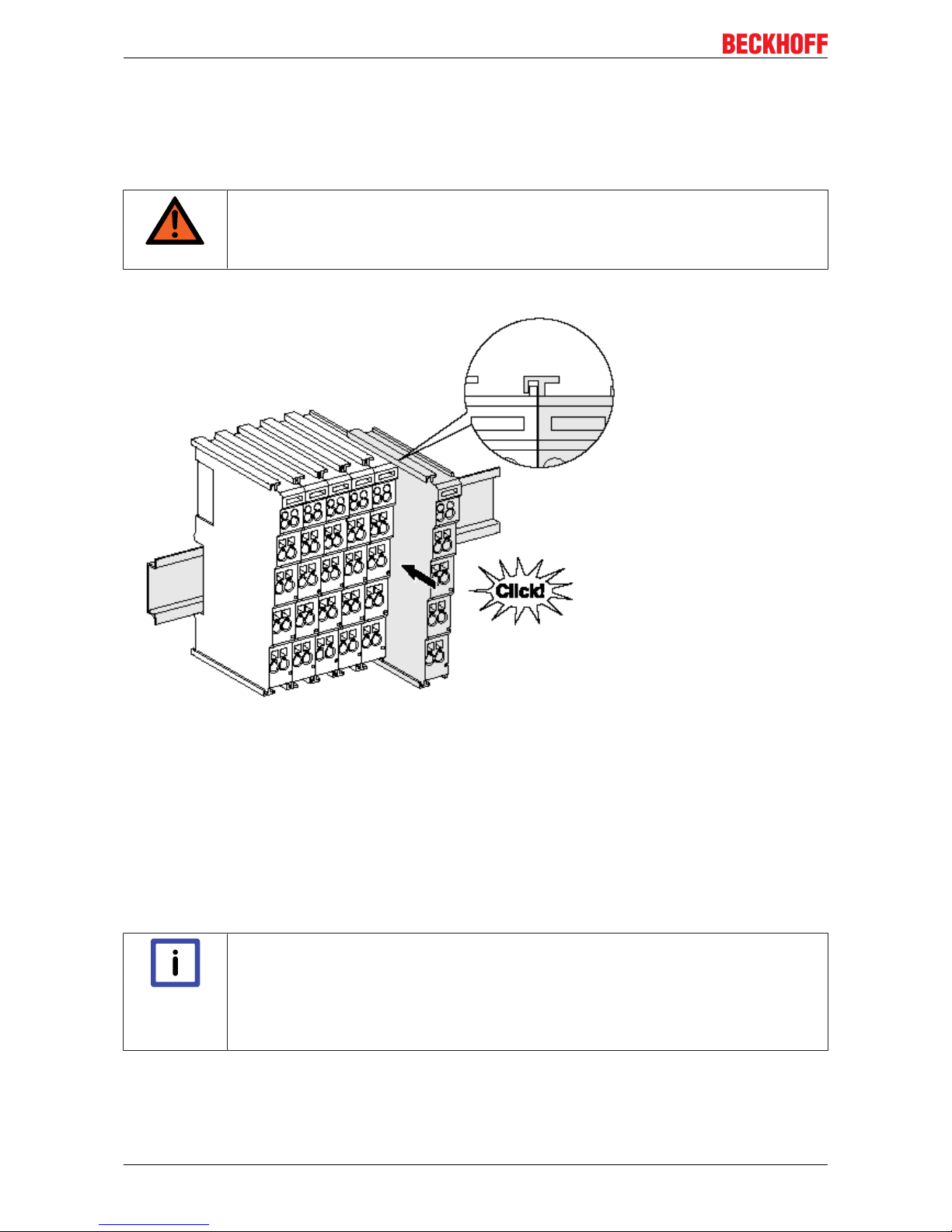
WARNING
Risk of electric shock and damage of device!
Bring the bus terminal system into a safe, powered down state before starting installation,
disassembly or wiring of the Bus Terminals!
Assembly
Fig.4: Attaching on mounting rail
The Bus Coupler and Bus Terminals are attached to commercially available 35mm mounting rails (DIN rails
according to EN60715) by applying slight pressure:
1. First attach the Fieldbus Coupler to the mounting rail.
2. The Bus Terminals are now attached on the right-hand side of the Fieldbus Coupler. Join the
components with tongue and groove and push the terminals against the mounting rail, until the lock
clicks onto the mounting rail.
If the Terminals are clipped onto the mounting rail first and then pushed together without tongue and
groove, the connection will not be operational! When correctly assembled, no significant gap should
be visible between the housings.
Note
Fixing of mounting rails
The locking mechanism of the terminals and couplers extends to the profile of the mounting
rail. At the installation, the locking mechanism of the components must not come into conflict with the fixing bolts of the mounting rail. To mount the mounting rails with a height of
7.5mm under the terminals and couplers, you should use flat mounting connections (e.g.
countersunk screws or blind rivets).
KL5151/KS5151, KL5152/KS515212 Version: 2.0.0
Page 13

Mounting and wiring
Disassembly
Fig.5: Disassembling of terminal
Each terminal is secured by a lock on the mounting rail, which must be released for disassembly:
1. Pull the terminal by its orange-colored lugs approximately 1cm away from the mounting rail. In doing
so for this terminal the mounting rail lock is released automatically and you can pull the terminal out of
the bus terminal block easily without excessive force.
2. Grasp the released terminal with thumb and index finger simultaneous at the upper and lower grooved
housing surfaces and pull the terminal out of the bus terminal block.
Connections within a bus terminal block
The electric connections between the Bus Coupler and the Bus Terminals are automatically realized by
joining the components:
• The six spring contacts of the K-Bus/E-Bus deal with the transfer of the data and the supply of the Bus
Terminal electronics.
• The power contacts deal with the supply for the field electronics and thus represent a supply rail within
the bus terminal block. The power contacts are supplied via terminals on the Bus Coupler (up to 24V)
or for higher voltages via power feed terminals.
Note
Power Contacts
During the design of a bus terminal block, the pin assignment of the individual Bus Terminals must be taken account of, since some types (e.g. analog Bus Terminals or digital 4channel Bus Terminals) do not or not fully loop through the power contacts. Power Feed
Terminals (KL91xx, KL92xx or EL91xx, EL92xx) interrupt the power contacts and thus represent the start of a new supply rail.
PE power contact
The power contact labeled PE can be used as a protective earth. For safety reasons this contact mates first
when plugging together, and can ground short-circuit currents of up to 125A.
KL5151/KS5151, KL5152/KS5152 13Version: 2.0.0
Page 14

Mounting and wiring
Fig.6: Power contact on left side
Attention
Possible damage of the device
Note that, for reasons of electromagnetic compatibility, the PE contacts are capacitatively
coupled to the mounting rail. This may lead to incorrect results during insulation testing or
to damage on the terminal (e.g. disruptive discharge to the PE line during insulation testing
of a consumer with a nominal voltage of 230V). For insulation testing, disconnect the PE
supply line at the Bus Coupler or the Power Feed Terminal! In order to decouple further
feed points for testing, these Power Feed Terminals can be released and pulled at least
10mm from the group of terminals.
WARNING
Risk of electric shock!
The PE power contact must not be used for other potentials!
4.2 Connection system
WARNING
Risk of electric shock and damage of device!
Bring the bus terminal system into a safe, powered down state before starting installation,
disassembly or wiring of the Bus Terminals!
Overview
The Bus Terminal system offers different connection options for optimum adaptation to the respective
application:
• The terminals of KLxxxx and ELxxxx series with standard wiring include electronics and connection
level in a single enclosure.
• The terminals of KSxxxx and ESxxxx series feature a pluggable connection level and enable steady
wiring while replacing.
• The High Density Terminals (HD Terminals) include electronics and connection level in a single
enclosure and have advanced packaging density.
KL5151/KS5151, KL5152/KS515214 Version: 2.0.0
Page 15

Mounting and wiring
Standard wiring
Fig.7: Standard wiring
The terminals of KLxxxx and ELxxxx series have been tried and tested for years.
They feature integrated screwless spring force technology for fast and simple assembly.
Pluggable wiring
Fig.8: Pluggable wiring
The terminals of KSxxxx and ESxxxx series feature a pluggable connection level.
The assembly and wiring procedure for the KS series is the same as for the KLxxxx and ELxxxx series.
The KS/ES series terminals enable the complete wiring to be removed as a plug connector from the top of
the housing for servicing.
The lower section can be removed from the terminal block by pulling the unlocking tab.
Insert the new component and plug in the connector with the wiring. This reduces the installation time and
eliminates the risk of wires being mixed up.
The familiar dimensions of the terminal only had to be changed slightly. The new connector adds about 3
mm. The maximum height of the terminal remains unchanged.
A tab for strain relief of the cable simplifies assembly in many applications and prevents tangling of individual
connection wires when the connector is removed.
Conductor cross sections between 0.08mm2 and 2.5mm2 can continue to be used with the proven spring
force technology.
The overview and nomenclature of the product names for KSxxxx and ESxxxx series has been retained as
known from KLxxxx and ELxxxx series.
High Density Terminals (HD Terminals)
Fig.9: High Density Terminals
The Bus Terminals from these series with 16 connection points are distinguished by a particularly compact
design, as the packaging density is twice as large as that of the standard 12mm Bus Terminals. Massive
conductors and conductors with a wire end sleeve can be inserted directly into the spring loaded terminal
point without tools.
KL5151/KS5151, KL5152/KS5152 15Version: 2.0.0
Page 16

Mounting and wiring
Note
Wiring HD Terminals
The High Density (HD) Terminals of the KLx8xx and ELx8xx series doesn't support steady
wiring.
Ultrasonically "bonded" (ultrasonically welded) conductors
Note
Ultrasonically “bonded" conductors
It is also possible to connect the Standard and High Density Terminals with ultrasonically
"bonded" (ultrasonically welded) conductors. In this case, please note the tables concern-
ing the wire-size width [}16] below!
Wiring
Terminals for standard wiring ELxxxx / KLxxxx and terminals for steady wiring
ESxxxx / KSxxxx
Fig.10: Mounting a cable on a terminal connection
Up to eight connections enable the connection of solid or finely stranded cables to the Bus Terminals. The
terminals are implemented in spring force technology. Connect the cables as follows:
1. Open a spring-loaded terminal by slightly pushing with a screwdriver or a rod into the square opening
above the terminal.
2. The wire can now be inserted into the round terminal opening without any force.
3. The terminal closes automatically when the pressure is released, holding the wire securely and
permanently.
Terminal housing ELxxxx, KLxxxx ESxxxx, KSxxxx
Wire size width 0.08 ... 2,5mm
2
0.08 ... 2.5mm
2
Wire stripping length 8 ... 9mm 9 ... 10mm
KL5151/KS5151, KL5152/KS515216 Version: 2.0.0
Page 17

Mounting and wiring
High Density Terminals ELx8xx, KLx8xx (HD)
The conductors of the HD Terminals are connected without tools for single-wire conductors using the direct
plug-in technique, i.e. after stripping the wire is simply plugged into the contact point. The cables are
released, as usual, using the contact release with the aid of a screwdriver. See the following table for the
suitable wire size width.
Terminal housing High Density Housing
Wire size width (conductors with a wire end sleeve) 0.14... 0.75mm
2
Wire size width (single core wires) 0.08 ... 1.5mm
2
Wire size width (fine-wire conductors) 0.25 ... 1.5mm
2
Wire size width (ultrasonically “bonded" conductors)
only 1.5mm2 (see notice
[}16]!)
Wire stripping length 8 ... 9mm
Shielding
Note
Shielding
Analog sensors and actors should always be connected with shielded, twisted paired wires.
KL5151/KS5151, KL5152/KS5152 17Version: 2.0.0
Page 18

Mounting and wiring
4.3 KL5151-0000 - Connection
WARNING
Risk of injury through electric shock and damage to the device!
Bring the Bus Terminals system into a safe, de-energized state before starting mounting,
disassembly or wiring of the Bus Terminals.
Fig.11: KL5151-0000
Pin assignment
Terminal point No. In the encoder interface operating mode*
Connection for
In the counter operating mode*
Connection for
A 1 Input A Counter input
+24 V 2 Power contact +24 V (internally connected to terminal point 6)
0 V 3 Power contact 0 V (internally connected to terminal point 7)
C 4 Input C or
zero input (in case bit 0 (EnLatchC [}29]) is set in the control byte, a
rising edge at this input causes the current counter value to be saved
in the latch register as a reference mark).
Counter enable (gate input for the
counter operating mode)
B 5 Input B Counting direction (high = down,
low = up)
+24 V 6 Power contact +24 V (internally connected to terminal point 2)
0 V 7 Power contact 0 V (internally connected to terminal point 3)
Gate/Latch 8 Gate input or
Latch input: if
• bit3 (EnLatchRise [}29]) is set in the control byte, a rising
edge
• bit 4 (EnLatchFall [}29]) is set in the control byte, a falling
edge
at this input causes the current counter value to be saved in the latch
register as a reference mark.
no function
*) The operating mode is set with bit R32.15 [}46] of the feature register.
KL5151/KS5151, KL5152/KS515218 Version: 2.0.0
Page 19

Mounting and wiring
4.4 KL5151-0021 - Connection
WARNING
Risk of injury through electric shock and damage to the device!
Bring the Bus Terminals system into a safe, de-energized state before starting mounting,
disassembly or wiring of the Bus Terminals.
Fig.12: KL5151-0021
Pin assignment
Terminal
point
No. Connection for
A 1 Input A
Output 2 Comparator output
0 V 3 Power contact 0 V (internally connected to terminal point 7)
C 4 Input C or
zero input (in case bit 0 (EnLatchC [}33]) is set in the control byte, a rising edge at
this input causes the current counter value to be saved in the latch register as a
reference mark).
B 5 Input B
+24 V 6 Power contact +24 V
0 V 7 Power contact 0 V (internally connected to terminal point 3)
Gate/Latch 8 Gate input or
Latch input: if
• bit3 (EnLatchRise [}33]) is set in the control byte, a rising edge
• bit 4 (EnLatchFall [}33]) is set in the control byte, a falling edge
at this input causes the current counter value to be saved in the latch register as a
reference mark.
KL5151/KS5151, KL5152/KS5152 19Version: 2.0.0
Page 20

Mounting and wiring
4.5 KL5152-0000 (KL5151-0050) - Connection
WARNING
Risk of injury through electric shock and damage to the device!
Bring the Bus Terminals system into a safe, de-energized state before starting mounting,
disassembly or wiring of the Bus Terminals.
Fig.13: KL5151-0050
Pin assignment
Terminal point No. Connection for
A1 1 Input A for encoder 1
+24 V 2 Power contact +24 V (internally connected to terminal point 6)
0 V 3 Power contact 0 V (internally connected to terminal point 7)
A2 4 Input A for encoder 2
B1 5 Input B for encoder 1
+24 V 6 Power contact +24 V (internally connected to terminal point 2)
0 V 7 Power contact 0 V (internally connected to terminal point 3)
B2 8 Input B for encoder 2
KL5151/KS5151, KL5152/KS515220 Version: 2.0.0
Page 21

Mounting and wiring
4.6 ATEX - Special conditions
WARNING
Observe the special conditions for the intended use of Beckhoff fieldbus
components in potentially explosive areas (directive 94/9/EU)!
ü Conditions
a) The certified components are to be installed in a suitable housing that guarantees a
protection class of at least IP54 in accordance with EN 60529! The environmental conditions during use are thereby to be taken into account!
b) If the temperatures during rated operation are higher than 70°C at the feed-in points of
cables, lines or pipes, or higher than 80°C at the wire branching points, then cables
must be selected whose temperature data correspond to the actual measured temperature values!
c) Observe the permissible ambient temperature range of 0 - 55°C for the use of Beckhoff
fieldbus components in potentially explosive areas!
d) Measures must be taken to protect against the rated operating voltage being exceeded
by more than 40% due to short-term interference voltages!
e) The individual terminals may only be unplugged or removed from the Bus Terminal sys-
tem if the supply voltage has been switched off or if a non-explosive atmosphere is ensured!
f) The connections of the certified components may only be connected or disconnected if
the supply voltage has been switched off or if a non-explosive atmosphere is ensured!
g) The fuses of the KL92xx/EL92xx power feed terminals may only be exchanged if the
supply voltage has been switched off or if a non-explosive atmosphere is ensured!
h) Address selectors and ID switches may only be adjusted if the supply voltage has been
switched off or if a non-explosive atmosphere is ensured!
Standards
The fundamental health and safety requirements are fulfilled by compliance with the following standards:
• EN 60079-0: 2006
• EN 60079-15: 2005
KL5151/KS5151, KL5152/KS5152 21Version: 2.0.0
Page 22

Mounting and wiring
Marking
The Beckhoff fieldbus components certified for potentially explosive areas bear one of the following
markings:
II 3 G Ex nA II T4 KEMA 10ATEX0075 X Ta: 0 - 55°C
or
II 3 G Ex nA nC IIC T4 KEMA 10ATEX0075 X Ta: 0 - 55°C
4.7 ATEX Documentation
Note
Notes about operation of the Beckhoff terminal systems in potentially explosive areas (ATEX)
Pay also attention to the continuative documentation Notes about operation of the Beckhoff
terminal systems in potentially explosive areas (ATEX) that is available in the download
area of the Beckhoff homepage http:\\www.beckhoff.com!
KL5151/KS5151, KL5152/KS515222 Version: 2.0.0
Page 23
Configuration software KS2000
5 Configuration software KS2000
5.1 KS2000 - Introduction
The KS2000 configuration software permits configuration, commissioning and parameterization of bus
couplers, of the affiliated bus terminals and of Fieldbus Box Modules. The connection between bus coupler/
Fieldbus Box Module and the PC is established by means of the serial configuration cable or the fieldbus.
Fig.14: KS2000 configuration software
Configuration
You can configure the Fieldbus stations with the Configuration Software KS2000 offline. That means, setting
up a terminal station with all settings on the couplers and terminals resp. the Fieldbus Box Modules can be
prepared before the commissioning phase. Later on, this configuration can be transferred to the terminal
station in the commissioning phase by means of a download. For documentation purposes, you are provided
with the breakdown of the terminal station, a parts list of modules used and a list of the parameters you have
modified. After an upload, existing fieldbus stations are at your disposal for further editing.
Parameterization
KS2000 offers simple access to the parameters of a fieldbus station: specific high-level dialogs are available
for all bus couplers, all intelligent bus terminals and Fieldbus Box modules with the aid of which settings can
be modified easily. Alternatively, you have full access to all internal registers of the bus couplers and
intelligent terminals. Refer to the register description for the meanings of the registers.
KL5151/KS5151, KL5152/KS5152 23Version: 2.0.0
Page 24

Configuration software KS2000
Commissioning
The KS2000 software facilitates commissioning of machine components or their fieldbus stations: Configured
settings can be transferred to the fieldbus modules by means of a download. After a login to the terminal
station, it is possible to define settings in couplers, terminals and Fieldbus Box modules directly online. The
same high-level dialogs and register access are available for this purpose as in the configuration phase.
The KS2000 offers access to the process images of the bus couplers and Fieldbus Box modules.
• Thus, the coupler's input and output images can be observed by monitoring.
• Process values can be specified in the output image for commissioning of the output modules.
All possibilities in the online mode can be used in parallel with the actual fieldbus mode of the terminal
station. The fieldbus protocol always has the higher priority in this case.
KL5151/KS5151, KL5152/KS515224 Version: 2.0.0
Page 25
Configuration software KS2000
5.2 Parameterization with KS2000
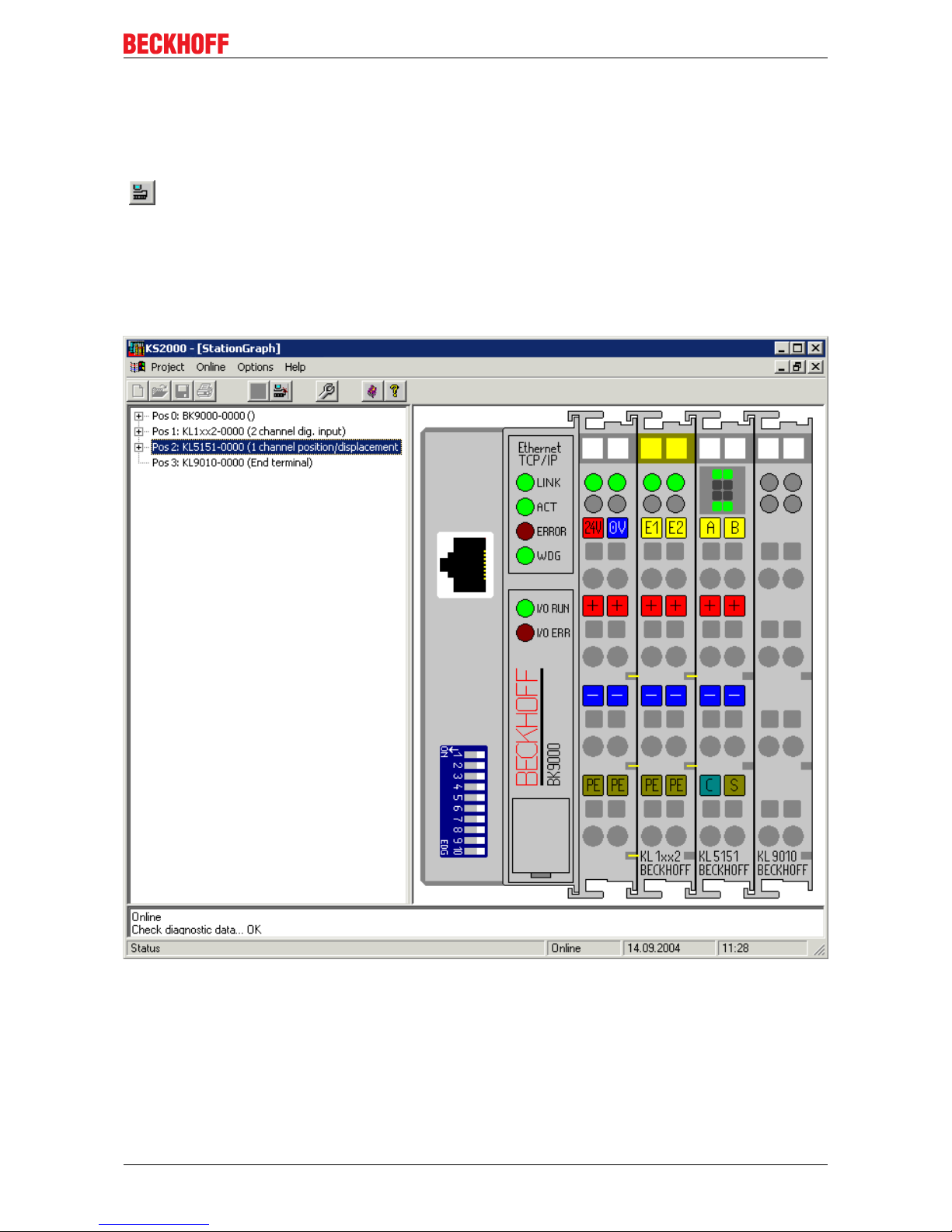
Connect the configuration interface of your fieldbus coupler with the serial interface of your PC via the
configuration cable and start the KS2000 configuration software.
Click on the Login button. The configuration software will now load the information for the
connected fieldbus station.
In the example shown, this is
• a BK9000 Ethernet coupler
• a KL1xx2 digital input terminal
• a KL5151-0000 incremental encoder terminal
• a KL9010 bus end terminal
Fig.15: Display of the fieldbus station in KS2000
The left-hand KS2000 window displays the terminals of the fieldbus station in a tree structure.
The right-hand KS2000 window contains a graphic display of the fieldbus station terminals.
In the tree structure of the left-hand window, click on the plus-sign next to the terminal whose parameters
you wish to change (item 2 in the example).
KL5151/KS5151, KL5152/KS5152 25Version: 2.0.0
Page 26
Configuration software KS2000
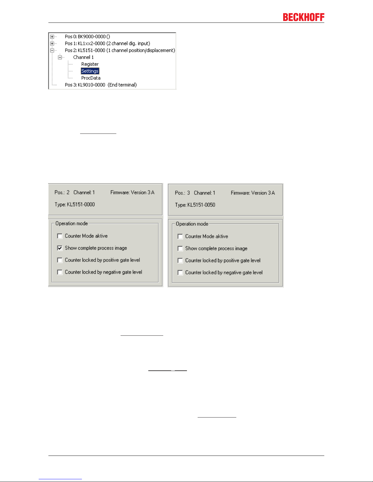
Fig.16: KS2000 tree branches for channel 1 of the KL5151
For the KL5151, the branches Register, Settings and ProcData are displayed:
• Register permits direct access to the registers of the KL5151.
• Under Settings [}26] you find dialog boxes for parameterizing the KL5151.
• ProcData displays the KL5151 process data.
5.3 Settings
The dialog mask for the parameterization of the KL5151-0000 or KL5151-0050 can be found under Settings.
Fig.17: Settings via KS2000
Operation mode
Counter mode active (R32.15 [}46])
You can activate counter mode here (default: inactive). When counter mode is activated, the KL5151-0000
operates as a 32 bit up/down counter.
Display whole process image (R32.6 [}46])
Meaningful operation of the KL5151-0000 is only possible with the full process image (default: active)!
The KL5151-0050 is factory-set to the small (compact) process image.
You can activate evaluation of the full process image for the KL5151-0050 here.
A positive level at the gate locks the counter (R32.5 [}46])
You can lock the counter by applying a positive level to the gate input (default: inactive).
KL5151/KS5151, KL5152/KS515226 Version: 2.0.0
Page 27

Configuration software KS2000
A negative level at the gate locks the counter (R32.4 [}46])
You can lock the counter by applying a negative level to the gate input (default: inactive).
KL5151/KS5151, KL5152/KS5152 27Version: 2.0.0
Page 28
Access from the user program
6 Access from the user program
6.1 KL5151-0000
6.1.1 Process image
In the process image, the KL5151 is represented with 5 bytes of input and output data. These are organized
as follows:
Format Input data Output data
Byte
SB [}30] CB [}29]
Double
word
DataIN DataOUT
Legend
SB: Status byte
CB: Control byte
DataIN: The current value of the 32-bit counter, or the one stored in the latch (the selection is made with bit
CB1.1 [}29] of the control byte)
DataOUT: Value specified for the 32 bit counter
• Please refer to the Mapping [}31] page for the allocation of the bytes and words to the addresses of
the controller.
• The meaning of the control and status bytes is explained on the Control and Status bytes [}29] page.
Note
No compact process image
Operation of the KL5151-0000 with compact process image (without control and status
bytes) is not possible, since the control and status bytes are required for useful process
data operation of the terminal. Even if you adjust your Bus Coupler to the compact process
image, the KL5151-0000 will still be represented with its complete process image!
KL5151/KS5151, KL5152/KS515228 Version: 2.0.0
Page 29
Access from the user program
6.1.2 Control and status bytes
Channel 1
Process data mode
Control byte 1 in process data mode
Control byte 1 (CB1) is located in the output image, and is transmitted from the controller to the terminal.
Bit CB1.7 CB1.6 CB1.5 CB1.4 CB1.3 CB1.2 CB1.1 CB1.0
Name RegAccess - RS_CNT_LATEnLatchFall EnLatchRise SetCnt ReadLatch EnLatchC
Legend
Bit Name Description
CB1.7 RegAccess 0
bin
Register communication off (process data mode)
CB1.6 - reserved
CB1.5 RS_CNT_LAT*1
bin
The counter is set to zero by an active edge at the latch input
[}18]. Bits CB1.4, CB1.3 and CB1.0 specify which edge of the
latch signal is active.
CB1.4 EnLatchFall* 1
bin
The falling edge of the latch input [}18] is active. The counter
value is stored in the latch register at the first external latch
impulse after the EnLatchFall bit becomes true. The
subsequent pulses do not have any effect on the latch register.
CB1.3 EnLatchRise*1
bin
The rising edge of the latch input [}18] is active. The counter
value is stored in the latch register on the first external latch
pulse after the EnLatchRise bit becomes true (this has priority
over EnLatchFall). The subsequent pulses do not have any
effect on the latch register.
CB1.2 SetCnt A rising edge at SetCnt will set the counter to the 32 bit value that is written by
the controller into the process output data.
CB1.1 ReadLatch 0
bin
The current value of the 32 bit counter is mapped to the
process input data.
1
bin
The 32 bit value stored in the latch counter is mapped to the
process input data.
CB1.0 EnLatchC* 1
bin
The rising edge of the zero input (input C [}18]) is active. The
counter value is stored in the latch register at the first external
latch impulse after the EnLatchC bit becomes true. The
subsequent pulses do not have any effect on the latch register.
(see note below)
*) Does not apply to KL5152-0000 (KL5151-0050), since the latch input and zero input are not available in
this case. Always set bits CB1.5, CB1.4, CB1.3 and CB1.0 of the KL5152-0000 (KL5151-0050) to 0
bin
!
Note
EnLatchC or EnLatchRise and EnLatchFall?
If bit CB1.0 (EnLatchC) is set, bit CB1.3 (EnLatchRise) and bit CB1.4 (EnLatchFall) must
not be set, otherwise you cannot know which event has caused a counter value to be
stored in the latch.
Status byte 1 in process data mode
The status byte 1 (SB1) is located in the input image, and is transmitted from terminal to the controller.
KL5151/KS5151, KL5152/KS5152 29Version: 2.0.0
Page 30
Access from the user program
Bit SB1.7 SB1.6 SB1.5 SB1.4 SB1.3 SB1.2 SB1.1 SB1.0
Name RegAccess- - StGate StLatchC SetCnt ReadLatchValLatchC
Legend
Bit Name Description
SB1.7 RegAccess 0
bin
Acknowledgement for process data mode
SB1.6 - reserved
SB1.5 - reserved
SB1.4 StGate
KL5151-0000: Status of the external gate/latch input [}18]
KL5152-0000 (KL5151-0050): reserved
SB1.3 StLatchC
KL5151-0000: Status of the zero input (input C [}18])
KL5152-0000 (KL5151-0050): reserved
SB1.2 SetCnt Acknowledgement that the data for setting the counter has been adopted by
the terminal.
SB1.1 ReadLatch 0
bin
The current value of the 32 bit counter has been mapped to the
process data.
1
bin
The 32 bit value stored in the latch counter has been mapped
to the process data.
SB1.0 ValLatchC* 1
bin
A zero-point latch has occurred: a rising edge at the zero input
(input C [}18]) has caused the current counter value to be
stored in the latch register as a reference mark.
Subsequent pulses do not have any effect on the latch register.
To reactivate the gate/latch input [}18] you must:
• set bit 0 (EnLatchC) in the control byte to 0
bin
.
• wait until this change has been acknowledged by
resetting bit 0 (ValLatchC) in the status byte.
• set bit 0 (EnLatchC) in the control byte to 1
bin
again.
*) Does not apply to KL5152-0000 (KL5151-0050), since the latch input and zero input are not available in
this case.
Register communication
Control byte 1 in register communication
Control byte 1 (CB1) is located in the output image, and is transmitted from the controller to the terminal.
Bit CB1.7 CB1.6 CB1.5 CB1.4 CB1.3 CB1.2 CB1.1 CB1.0
Name RegAccess R/W Reg. no.
Legend
Bit Name Description
CB1.7 RegAccess 1
bin
Register communication switched on
CB1.6 R/W 0
bin
Read access
1
bin
Write access
CB1.5 to
CB1.0
Reg. no. Register number:
Enter the number of the register [}44] that you
- want to read with input data word 0 or
- write to with output data word 0.
KL5151/KS5151, KL5152/KS515230 Version: 2.0.0
Page 31

Access from the user program
CAUTION
No valid process data during the register communication!
It is not possible to access the data registers during register communication! Process data
that may still be displayed is not valid!
Status byte 1 in register communication
The status byte 1 (SB1) is located in the input image, and is transmitted from terminal to the controller.
Bit SB1.7 SB1.6 SB1.5 SB1.4 SB1.3 SB1.2 SB1.1 SB1.0
Name RegAccess R Reg. no.
Legend
Bit Name Description
SB1.7 RegAccess 1
bin
Acknowledgement for register access
SB1.6 R 0
bin
Read access
SB1.5 to
SB1.0
Reg. no. Number of the register that was read or written.
Channel 2 (KL5152-0000 and KL5151-0050 only)
The control and status bytes of channel 2 (CB2 and SB2) have the same structure as the control and status
bytes of channel 1 [}29].
6.1.3 Mapping
The Bus Terminals occupy addresses within the process image of the controller. The assignment of process
data (input and output data) and parameterization data (control and status bytes) to the control addresses is
called mapping. The type of mapping depends on:
• the fieldbus system used
• the terminal type
• the parameterization of the Bus Coupler such as
- Intel or Motorola format
- word alignment switched on or off
The Bus Couplers (BKxxxx, LCxxxx) and Bus Terminal Controllers (BCxxxx, BXxxxx) are supplied with
certain default settings. The default setting can be changed with the KS2000 configuration software or with a
master configuration software (e.g. TwinCAT System Manager or ComProfibus).
The following tables show the mapping depending on different conditions. For information about the contents
of the individual bytes please refer to the pages Process image [}28] and Control and status byte [}29].
Complete evaluation
Control and status bytes can be accessed.
Complete evaluation in Intel format
Default mapping for CANopen, CANCAL, DeviceNet, ControlNet, Modbus, RS232 and RS485 coupler.
Parameterization
of the Bus Coupler
Address Input data Output data
Word offset High byte Low byte High byte Low byte
Complete evaluation: n/a
Motorola format: no
Word alignment: no
0 DataIN D0 SB DataOUT D0 CB
1 DataIN D2 DataIN D1 DataOUT D2 DataOUT D1
2 reserved DataIN D3 reserved DataOUT D3
KL5151/KS5151, KL5152/KS5152 31Version: 2.0.0
Page 32

Access from the user program
Complete evaluation in Motorola format
Parameterization
of the Bus Coupler
Address Input data Output data
Word offset High byte Low byte High byte Low byte
Complete evaluation: n/a
Motorola format: yes
Word alignment: no
0 DataIN D3 SB DataOUT D3 CB
1 DataIN D1 DataIN D2 DataOUT D1 DataOUT D2
2 reserved DataIN D0 reserved DataOUT D0
Complete evaluation in Intel format with word alignment
Default mapping for EtherCAT, Lightbus and Ethernet coupler as well as Bus Terminal Controllers (BCxxxx,
BXxxxx).
Parameterization
of the Bus Coupler
Address Input data Output data
Word offset High byte Low byte High byte Low byte
Complete evaluation: n/a
Motorola format: no
Word alignment: yes
0 reserved SB reserved CB
1 DataIN D1 DataIN D0 DataOUT D1 DataOUT D0
2 DataIN D3 DataIN D2 DataOUT D3 DataOUT D2
Complete evaluation in Motorola format with word alignment
Parameterization
of the Bus Coupler
Address Input data Output data
Word offset High byte Low byte High byte Low byte
Complete evaluation: n/a
Motorola format: yes
Word alignment: yes
0 reserved SB1 reserved CB1
1 DataIN D2 DataIN D3 DataOUT D2 DataOUT D3
2 DataIN D0 DataIN D1 DataOUT D0 DataOUT D1
Legend
Complete evaluation: In addition to the process data, the control and status bytes are also mapped into the
address space.
Motorola format: Motorola or Intel format can be set.
Word alignment: In order for the word address range to commence at a word boundary, empty bytes are
inserted into the process image as appropriate.
SB: Status byte (appears in the input process image)
CB: Control byte (appears in the output process image)
DataIN D0: Input double word, lowest significant data byte
DataIN D1: Input double word, ...
DataIN D2: Input double word, ...
DataIN D3: Input double word, highest significant data byte
DataOUT D0: Output double word, lowest significant data byte
DataOUT D1: Output double word, ...
DataOUT D2: Output double word, ...
DataOUT D3: Output double word, highest significant data byte
reserved: This byte occupies process data memory, although it has no function.
Compact evaluation
Note
No compact process image
Operation of the KL5151-0000 with compact process image (without control and status
bytes) is not possible, since the control and status bytes are required for useful process
data operation of the terminal. Even if you adjust your Bus Coupler to the compact process
image, the KL5151-0000 will still be represented with its complete process image!
KL5151/KS5151, KL5152/KS515232 Version: 2.0.0
Page 33

Access from the user program
6.2 KL5151-0021
6.2.1 Process image
In the process image, the KL5151 is represented with 5 bytes of input and output data. These are organized
as follows:
Format Input data Output data
Byte
SB1 [}33] CB1 [}33]
Double
word
DataIN1 DataOUT1
Byte SB2 CB2
Double
word
DataIN2 DataOUT2
Legend
SB1: Status byte 1
CB1: Control byte 1
SB1: Status byte 2 (not used)
CB1: Control byte 2 (not used)
DataIN1: The current value of the 32-bit counter, or the one stored in the latch (the selection is made with bit
CB1.1 [}33] of the control byte)
DataOUT1: Compare value for setting the comparator output (enabled by bit CB1.6 [}33] of the control
byte).
DataIN2: 32-bit latch
DataOUT2: Compare value for resetting the comparator output
• The meaning of the control and status bytes is explained on the Control and Status bytes [}33] page.
Note
No compact process image
Operation of the KL5151-0021 with compact process image (without control and status
bytes) is not possible, since the control and status bytes are required for useful process
data operation of the terminal. Even if you adjust your Bus Coupler to the compact process
image, the KL5151-0021 will still be represented with its complete process image!
6.2.2 Control and status bytes
Control byte 1 and status byte 1
Process data mode
Control byte 1 in process data mode
Control byte 1 (CB1) is located in the output image, and is transmitted from the controller to the terminal.
Bit CB1.7 CB1.6 CB1.5 CB1.4 CB1.3 CB1.2 CB1.1 CB1.0
Name RegAccess EnComp SetOut ReadLatchN ReadLatchP SetCnt EnMeas EnLatchC
KL5151/KS5151, KL5152/KS5152 33Version: 2.0.0
Page 34

Access from the user program
Legend
Bit Name Description
CB1.7 RegAccess 0
bin
Register communication off (process data mode)
CB1.6 EnComp 0
bin
Compare function for setting and resetting the output not enabled
1
bin
Compare function for setting and resetting the output enabled
CB1.5 SetOut 0
bin
sets output manually to 0 V SetOut only functions if EnComp =
0
bin
1
bin
sets output manually to 24 V
CB1.4 ReadLatchN 1
bin
Read the negative edge
CB1.3 ReadLatchP 1
bin
Read the positive edge
CB1.2 SetCnt A rising edge at SetCnt will set the counter to the 32 bit value that is written
by the controller into the process output data.
CB1.1 EnMeas 0
bin
Workpiece measurement
enabled
If the workpiece measurement is
enabled, it is read via CB1.3 and
CB1.4 and saved in two latch values.
1
bin
Workpiece measurement not
enabled
CB1.0 EnLatchC 1
bin
The rising edge of the zero input (input C [}19]) is active. The
counter value is stored in the latch register at the first external latch
impulse after the EnLatchC bit becomes true. The subsequent pulses
do not have any effect on the latch register. (see note below)
Note
EnLatchC or EnLatchRise and EnLatchFall?
If bit CB1.0 (EnLatchC) is set, bit CB1.3 (EnLatchRise) and bit CB1.4 (EnLatchFall) must
not be set, otherwise you cannot know which event has caused a counter value to be
stored in the latch.
Status byte 1 in process data mode
The status byte 1 (SB1) is located in the input image, and is transmitted from terminal to the controller.
Bit SB1.7 SB1.6 SB1.5 SB1.4 SB1.3 SB1.2 SB1.1 SB1.0
Name RegAccess - StOut StGate StLatchC SetCnt MeasDone ValLatchC
Legend
Bit Name Description
SB1.7 RegAccess 0
bin
Acknowledgement for process data mode
SB1.6 - reserved
SB1.5 StOut 0
bin
Status of the output is 0 V
1
bin
Status of the output is 24 V
SB1.4 StGate
Status of the external gate/latch input [}19]
SB1.3 StLatchC Status of the zero input (input C)
SB1.2 SetCnt Acknowledgement that the data for setting the counter has been adopted by
the terminal.
SB1.1 MeasDone 1
bin
Measurement done
SB1.0 ValLatchC 1
bin
A zero-point latch has occurred: a rising edge at the zero input (input
C [}19]) has caused the current counter value to be stored in the
latch register as a reference mark.
Subsequent pulses do not have any effect on the latch register. To
reactivate the gate/latch input [}19] you must:
• set bit 0 (EnLatchC) in the control byte to 0
bin
.
• wait until this change has been acknowledged by resetting bit 0
(ValLatchC) in the status byte.
• set bit 0 (EnLatchC) in the control byte to 1
bin
again.
KL5151/KS5151, KL5152/KS515234 Version: 2.0.0
Page 35

Access from the user program
Register communication
Control byte 1 in register communication
Control byte 1 (CB1) is located in the output image, and is transmitted from the controller to the terminal.
Bit CB1.7 CB1.6 CB1.5 CB1.4 CB1.3 CB1.2 CB1.1 CB1.0
Name RegAccess R/W Reg. no.
Legend
Bit Name Description
CB1.7 RegAccess 1
bin
Register communication switched on
CB1.6 R/W 0
bin
Read access
1
bin
Write access
CB1.5 to CB1.0 Reg. no. Register number:
Enter the number of the register [}44] that you
- want to read with input data word 0 or
- write to with output data word 0.
CAUTION
No valid process data during the register communication!
It is not possible to access the data registers during register communication! Process data
that may still be displayed is not valid!
Status byte 1 in register communication
The status byte 1 (SB1) is located in the input image, and is transmitted from terminal to the controller.
Bit SB1.7 SB1.6 SB1.5 SB1.4 SB1.3 SB1.2 SB1.1 SB1.0
Name RegAccess R Reg. no.
Legend
Bit Name Description
SB1.7 RegAccess 1
bin
Acknowledgement for register access
SB1.6 R 0
bin
Read access
SB1.5 to SB1.0 Reg. no. Number of the register that was read or written.
Control byte 2 and status byte 2
Control byte 2 and status byte 2 (CB2 and SB2) are not used.
6.3 KL5152-0000 (KL5150-0050)
6.3.1 Process image
The terminal can be operated with variously sized process images:
• compact process image
• compact process image on Bus Coupler that is set to complete process image (e.g. Lightbus)
• complete process image
The compact process image is activated in the delivery condition of the KL5151-0050. The size of the
process image can be specified through bit R32.6 [}46] of the feature register.
KL5151/KS5151, KL5152/KS5152 35Version: 2.0.0
Page 36

Access from the user program
Control byte, status byte and mapping
• The meaning of the control and status bytes is explained on the Control and Status bytes [}29] page.
• Please refer to the Mapping [}40] page for the allocation of the bytes and words to the addresses of
the controller.
Compact process image
For operation with compact process image, you must configure your Bus Coupler to compact mapping and
bit R32.6 [}46] of the feature register of the KL5151-0050 must be 1
bin
.
The KL5151-0050 is represented in the compact process image with 8 bytes of input data and 8 bytes of
output data. These are organized as follows:
Input data Output data
Format Contents Format Contents
Double
word
DataIN1 Byte
CB1PD [}29]
Byte reserved
Byte
CB2PD [}31]
Byte reserved
Double
word
DataIN2 Double
word
DataOUT
Legend
CB1PD: Control byte for process data operation of channel 1
CB2PD: Control byte for process data operation of channel 2
DataIN1: The current value of the 32-bit counter 1, or the one stored in the latch (the selection is made with
bit CB1.1 [}29] of the control byte 1)
DataIN2: The current value of the 32-bit counter 2, or the one stored in the latch (the selection is made with
bit CB2.1 [}31] of the control byte 2)
DataOUT: 32 bit specification of the value for counter 1 and counter 2
Note
No register communication possible
In this configuration the control bytes are suitable only for process data operation. Register
communication is not possible!
Complete process image
For operation with complete process image, you must configure your Bus Coupler to complete mapping and
bit R32.6 [}46] of the feature register of the KL5151-0050 must be 0
bin
.
The KL5151-0050 is represented in the complete process image with 10 bytes of input data and 10 bytes of
output data. These are organized as follows:
Input data Output data
Format Contents Format Contents
Byte
SB1 [}30]
Byte
CB1 [}29]
Double
word
DataIN1 Double
word
DataOUT1
Byte
SB2 [}31]
Byte
CB2 [}31]
Double
word
DataIN2 Double
word
DataOUT2
KL5151/KS5151, KL5152/KS515236 Version: 2.0.0
Page 37
Access from the user program
Legend
SB1: Status byte for channel 1
SB2: Status byte for channel 2
CB1: Control byte for channel 1
CB2: Control byte for channel 2
DataIN1: The current value of the 32-bit counter 1, or the one stored in the latch (the selection is made with
bit CB1.1 [}29] of the control byte 1)
DataIN2: The current value of the 32-bit counter 2, or the one stored in the latch (the selection is made with
bit CB2.1 [}31] of the control byte 2)
DataOUT1: 32 bit specification of the value for counter 1
DataOUT2: 32 bit specification of the value for counter 2
Note
Register communication possible
In this configuration you can use the control and status bytes alternatively for register communication or process data operation.
Compact process image on Bus Coupler that is set to complete process image
If the KL5151-0050 is operated on a Bus Coupler that is set by default to complete process image (e.g.
Lightbus), but bit R32.6 [}46] of the feature register is 1
bin
, the following process image results:
Input data Output data
Format Contents Format Contents
Byte
SB1RC [}31]
Byte
CB1RC [}30]
Double
word
DataIN1 Byte
CB1PD [}29]
Byte reserved
Byte
CB2PD [}31]
Byte reserved
Byte
SB2RC [}31]
Byte
CB2RC [}31]
Double
word
DataIN2 Double
word
DataOUT
Legend
SB1RC: Status byte for register communication with channel 1
SB2RC: Status byte for register communication with channel 2
CB1RC: Control byte for register communication with channel 1
CB2RC: Control byte for register communication with channel 2
CB1PD: Control byte for process data operation of channel 1
CB2PD: Control byte for process data operation of channel 2
DataIN1: The current value of the 32-bit counter 1, or the one stored in the latch (the selection is made with
bit CB1.1 [}29] of the control byte 1)
DataIN2: The current value of the 32-bit counter 2, or the one stored in the latch (the selection is made with
bit CB2.1 [}31] of the control byte 2)
DataOUT: 32 bit specification of the value for counter 1 and counter 2
Note
Register communication possible
In this configuration you have different control and status bytes for register communication
and process data operation. These are only suitable for the respectively specified purpose!
You can switch from process data operation to register communication with bit 7 of the control byte for register communication.
Bit 7 of the control byte for process data operation is not evaluated.
KL5151/KS5151, KL5152/KS5152 37Version: 2.0.0
Page 38

Access from the user program
6.3.2 Control and status bytes
Channel 1
Process data mode
Control byte 1 in process data mode
Control byte 1 (CB1) is located in the output image, and is transmitted from the controller to the terminal.
Bit CB1.7 CB1.6 CB1.5 CB1.4 CB1.3 CB1.2 CB1.1 CB1.0
Name RegAccess - RS_CNT_LATEnLatchFall EnLatchRise SetCnt ReadLatch EnLatchC
Legend
Bit Name Description
CB1.7 RegAccess 0
bin
Register communication off (process data mode)
CB1.6 - reserved
CB1.5 RS_CNT_LAT*1
bin
The counter is set to zero by an active edge at the latch input [}18].
Bits CB1.4, CB1.3 and CB1.0 specify which edge of the latch signal
is active.
CB1.4 EnLatchFall* 1
bin
The falling edge of the latch input [}18] is active. The counter value
is stored in the latch register at the first external latch impulse after
the EnLatchFall bit becomes true. The subsequent pulses do not
have any effect on the latch register.
CB1.3 EnLatchRise* 1
bin
The rising edge of the latch input [}18] is active. The counter value
is stored in the latch register on the first external latch pulse after the
EnLatchRise bit becomes true (this has priority over EnLatchFall).
The subsequent pulses do not have any effect on the latch register.
CB1.2 SetCnt A rising edge at SetCnt will set the counter to the 32 bit value that is written
by the controller into the process output data.
CB1.1 ReadLatch 0
bin
The current value of the 32 bit counter is mapped to the process
input data.
1
bin
The 32 bit value stored in the latch counter is mapped to the process
input data.
CB1.0 EnLatchC* 1
bin
The rising edge of the zero input (input C [}18]) is active. The
counter value is stored in the latch register at the first external latch
impulse after the EnLatchC bit becomes true. The subsequent pulses
do not have any effect on the latch register. (see note below)
*) Does not apply to KL5152-0000 (KL5151-0050), since the latch input and zero input are not available in
this case. Always set bits CB1.5, CB1.4, CB1.3 and CB1.0 of the KL5152-0000 (KL5151-0050) to 0
bin
!
Note
EnLatchC or EnLatchRise and EnLatchFall?
If bit CB1.0 (EnLatchC) is set, bit CB1.3 (EnLatchRise) and bit CB1.4 (EnLatchFall) must
not be set, otherwise you cannot know which event has caused a counter value to be
stored in the latch.
Status byte 1 in process data mode
The status byte 1 (SB1) is located in the input image, and is transmitted from terminal to the controller.
Bit SB1.7 SB1.6 SB1.5 SB1.4 SB1.3 SB1.2 SB1.1 SB1.0
Name RegAccess - - StGate StLatchC SetCnt ReadLatch ValLatchC
KL5151/KS5151, KL5152/KS515238 Version: 2.0.0
Page 39

Access from the user program
Legend
Bit Name Description
SB1.7 RegAccess 0
bin
Acknowledgement for process data mode
SB1.6 - reserved
SB1.5 - reserved
SB1.4 StGate
KL5151-0000: Status of the external gate/latch input [}18]
KL5152-0000 (KL5151-0050): reserved
SB1.3 StLatchC
KL5151-0000: Status of the zero input (input C [}18])
KL5152-0000 (KL5151-0050): reserved
SB1.2 SetCnt Acknowledgement that the data for setting the counter has been adopted
by the terminal.
SB1.1 ReadLatch 0
bin
The current value of the 32 bit counter has been mapped to the
process data.
1
bin
The 32 bit value stored in the latch counter has been mapped to the
process data.
SB1.0 ValLatchC* 1
bin
A zero-point latch has occurred: a rising edge at the zero input (input
C [}18]) has caused the current counter value to be stored in the
latch register as a reference mark.
Subsequent pulses do not have any effect on the latch register. To
reactivate the gate/latch input [}18] you must:
• set bit 0 (EnLatchC) in the control byte to 0
bin
.
• wait until this change has been acknowledged by resetting bit 0
(ValLatchC) in the status byte.
• set bit 0 (EnLatchC) in the control byte to 1
bin
again.
*) Does not apply to KL5152-0000 (KL5151-0050), since the latch input and zero input are not available in
this case.
Register communication
Control byte 1 in register communication
Control byte 1 (CB1) is located in the output image, and is transmitted from the controller to the terminal.
Bit CB1.7 CB1.6 CB1.5 CB1.4 CB1.3 CB1.2 CB1.1 CB1.0
Name RegAccess R/W Reg. no.
Legend
Bit Name Description
CB1.7 RegAccess 1
bin
Register communication switched on
CB1.6 R/W 0
bin
Read access
1
bin
Write access
CB1.5 to CB1.0 Reg. no. Register number:
Enter the number of the register [}44] that you
- want to read with input data word 0 or
- write to with output data word 0.
CAUTION
No valid process data during the register communication!
It is not possible to access the data registers during register communication! Process data
that may still be displayed is not valid!
KL5151/KS5151, KL5152/KS5152 39Version: 2.0.0
Page 40

Access from the user program
Status byte 1 in register communication
The status byte 1 (SB1) is located in the input image, and is transmitted from terminal to the controller.
Bit SB1.7 SB1.6 SB1.5 SB1.4 SB1.3 SB1.2 SB1.1 SB1.0
Name RegAccess R Reg. no.
Legend
Bit Name Description
SB1.7 RegAccess 1
bin
Acknowledgement for register access
SB1.6 R 0
bin
Read access
SB1.5 to SB1.0 Reg. no. Number of the register that was read or written.
Channel 2 (KL5152-0000 and KL5151-0050 only)
The control and status bytes of channel 2 (CB2 and SB2) have the same structure as the control and status
bytes of channel 1 [}38].
6.3.3 Mapping
The Bus Terminals occupy addresses within the process image of the controller. The assignment of process
data (input and output data) and parameterization data (control and status bytes) to the control addresses is
called mapping. The type of mapping depends on:
• the fieldbus system used
• the terminal type
• the parameterization of the Bus Coupler such as
- compact or full evaluation
- Intel or Motorola format
- word alignment switched on or off
• the parameterization of the KL5152-0000 (KL5151-0050) to compact or complete evaluation (bit R32.6
[}46] of the feature register)
The Bus Couplers (BKxxxx, LCxxxx) and Bus Terminal Controllers (BCxxxx, BXxxxx) are supplied with
certain default settings. The default setting can be changed with the KS2000 configuration software or with a
master configuration software (e.g. TwinCAT System Manager or ComProfibus).
The following tables show the mapping depending on different conditions. For information about the contents
of the individual bytes please refer to the pages Process image [}35] and Control and status byte [}29].
Compact evaluation
For operation with compact process image, you must configure your Bus Coupler to compact mapping and
bit R32.6 [}46] of the feature register of the KL5152-0000 (KL5151-0050) must be 1
bin
.
In this configuration the control bytes are suitable only for process data operation. Register communication is
not possible!
Compact evaluation in Intel format
Default mapping for CANopen, CANCAL, DeviceNet, ControlNet, Modbus, RS232 and RS485 coupler
KL5151/KS5151, KL5152/KS515240 Version: 2.0.0
Page 41

Access from the user program
Parameterization
of the Bus Coupler
Address Input data Output data
Word offset High byte Low byte High byte Low byte
Complete evaluation: no
Motorola format: no
Word alignment: n/a
0 DataIN1 D1 DataIN1 D0 reserved CB1PD
1 DataIN1 D3 DataIN1 D2 reserved CB2PD
2 DataIN2 D1 DataIN2 D0 DataOUT D1 DataOUT D0
3 DataIN2 D3 DataIN2 D2 DataOUT D3 DataOUT D2
Compact evaluation in Motorola format
Default mapping for PROFIBUS and Interbus coupler
Parameterization
of the Bus Coupler
Address Input data Output data
Word offset High byte Low byte High byte Low byte
Complete evaluation: no
Motorola format: yes
Word alignment: n/a
0 DataIN1 D2 DataIN1 D3 CB2PD reserved
1 DataIN1 D0 DataIN1 D1 CB1PD reserved
2 DataIN2 D2 DataIN2 D3 DataOUT D2 DataOUT D3
3 DataIN2 D0 DataIN2 D1 DataOUT D0 DataOUT D1
Complete evaluation
For operation with complete process image, you must configure your Bus Coupler to complete mapping and
bit R32.6 [}46] of the feature register of the KL5151-0050 must be 0
bin
.
In this configuration you can use the control and status bytes alternatively for register communication or
process data operation.
Complete evaluation in Intel format
Parameterization
of the Bus Coupler
Address Input data Output data
Word offset High byte Low byte High byte Low byte
Complete evaluation: yes
Motorola format: no
Word alignment: no
0 DataIN1 D0 SB1 DataOUT1 D0 CB1
1 DataIN1 D2 DataIN1 D1 DataOUT1 D2 DataOUT1 D1
2 SB2 DataIN1 D3 CB2 DataOUT1 D3
3 DataIN2 D1 DataIN2 D0 DataOUT2 D1 DataOUT2 D0
4 DataIN2 D3 DataIN2 D2 DataOUT2 D3 DataOUT2 D2
Complete evaluation in Motorola format
Parameterization
of the Bus Coupler
Address Input data Output data
Word offset High byte Low byte High byte Low byte
Complete evaluation: yes
Motorola format: yes
Word alignment: no
0 DataIN1 D3 SB1 DataOUT1 D3 CB1
1 DataIN1 D1 DataIN1 D2 DataOUT1 D1 DataOUT1 D2
2 SB2 DataIN1 D0 CB2 DataOUT1 D0
3 DataIN2 D2 DataIN2 D3 DataOUT2 D2 DataOUT2 D3
4 DataIN2 D0 DataIN2 D1 DataOUT2 D0 DataOUT2 D1
KL5151/KS5151, KL5152/KS5152 41Version: 2.0.0
Page 42
Access from the user program
Complete evaluation in Intel format with word alignment
Parameterization
of the Bus Coupler
Address Input data Output data
Word offset High byte Low byte High byte Low byte
Complete evaluation: yes
Motorola format: no
Word alignment: yes
0 reserved SB1 reserved CB1
1 DataIN1 D1 DataIN1 D0 DataOUT1 D1 DataOUT1 D0
2 DataIN1 D3 DataIN1 D2 DataOUT1 D3 DataOUT1 D2
3 reserved SB2 reserved CB2
4 DataIN2 D1 DataIN2 D0 DataOUT2 D1 DataOUT2 D0
5 DataIN2 D3 DataIN2 D2 DataOUT2 D3 DataOUT2 D2
Complete evaluation in Motorola format with word alignment
Parameterization
of the Bus Coupler
Address Input data Output data
Word offset High byte Low byte High byte Low byte
Complete evaluation: yes
Motorola format: yes
Word alignment: yes
0 reserved SB1 reserved CB1
1 DataIN1 D2 DataIN1 D3 DataOUT1 D2 DataOUT1 D3
2 DataIN1 D0 DataIN1 D1 DataOUT1 D0 DataOUT1 D1
3 reserved SB2 reserved CB2
4 DataIN2 D2 DataIN2 D3 DataOUT2 D2 DataOUT2 D3
5 DataIN2 D0 DataIN2 D1 DataOUT2 D0 DataOUT2 D1
Compact process image on Bus Coupler that is set to complete process image
If the KL5152-0000 (KL5151-0050) is operated on a Bus Coupler that is set by default to complete process
image (e.g. Lightbus), but bit R32.6 [}46] of the feature register is 1
bin
(default setting), the following process
image results:
In this configuration you have different control and status bytes for register communication and process data
operation. These are only suitable for the respectively specified purpose!
Intel format
Parameterization
of the Bus Coupler
Address Input data Output data
Word offset High byte Low byte High byte Low byte
Complete evaluation: yes
Motorola format: no
Word alignment: no
0 DataIN1 D0 SB1RC CB1PD CB1RC
1 DataIN1 D2 DataIN1 D1 CB2PD reserved
2 SB2RC DataIN1 D3 CB2RC reserved
3 DataIN2 D1 DataIN2 D0 DataOUT D1 DataOUT D0
4 DataIN2 D3 DataIN2 D2 DataOUT D3 DataOUT D2
Motorola format
Parameterization
of the Bus Coupler
Address Input data Output data
Word offset High byte Low byte High byte Low byte
Complete evaluation: yes
Motorola format: yes
Word alignment: no
0 DataIN1 D3 SB1RC reserved CB1RC
1 DataIN1 D1 DataIN1 D2 reserved CB2PD
2 SB2RC DataIN1 D0 CB2RC CB1PD
3 DataIN2 D2 DataIN2 D3 DataOUT D2 DataOUT D3
4 DataIN2 D0 DataIN2 D1 DataOUT D0 DataOUT D1
Intel format with word alignment
Default mapping for EtherCAT, Lightbus and Ethernet coupler as well as Bus Terminal Controllers (BCxxxx,
BXxxxx)
KL5151/KS5151, KL5152/KS515242 Version: 2.0.0
Page 43

Access from the user program
Parameterization
of the Bus Coupler
Address Input data Output data
Word offset High byte Low byte High byte Low byte
Complete evaluation: yes
Motorola format: no
Word alignment: yes
0 reserved SB1RC reserved CB1RC
1 DataIN1 D1 DataIN1 D0 reserved CB1PD
2 DataIN1 D3 DataIN1 D2 reserved CB2PD
3 reserved SB2RC reserved CB2RC
4 DataIN2 D1 DataIN2 D0 DataOUT D1 DataOUT D0
5 DataIN2 D3 DataIN2 D2 DataOUT D3 DataOUT D2
Motorola format with word alignment
Parameterization
of the Bus Coupler
Address Input data Output data
Word offset High byte Low byte High byte Low byte
Complete evaluation: yes
Motorola format: yes
Word alignment: yes
0 reserved SB1RC reserved CB1RC
1 DataIN1 D2 DataIN1 D3 CB2PD reserved
2 DataIN1 D0 DataIN1 D1 CB1PD reserved
3 reserved SB2RC reserved CB2RC
4 DataIN2 D2 DataIN2 D3 DataOUT D2 DataOUT D3
5 DataIN2 D0 DataIN2 D1 DataOUT D0 DataOUT D1
Legend
Complete evaluation: In addition to the process data, the control and status bytes are also mapped into the
address space.
Motorola format: Motorola or Intel format can be set.
Word alignment: In order for the channel address range to commence at a word boundary, empty bytes are
inserted into the process image as appropriate.
SB n: Status byte for channel n (appears in the input process image).
CB n: Control byte for channel n (appears in the output process image).
SB n PD: Status byte for channel n, to be used only for process data operation (appears in the input process
image)
CB n PD: Control byte for channel n, to be used only for process data operation (appears in the output
process image)
SB n RC: Status byte for channel n, to be used only for register communication (appears in the input process
image)
CB n RC: Control byte for channel n, to be used only for register communication (appears in the output
process image)
DataIN n D0: Channel n, input double word, lowest significant data byte
DataIN n D1: Channel n, input double word, ...
DataIN n D2: Channel n, input double word, ...
DataIN n D3: Channel n, input double word, highest significant data byte
DataOUT n D0: Channel n, output double word, lowest significant data byte
DataOUT n D1: Channel n, output double word, ...
DataOUT n D2: Channel n, output double word, ...
DataOUT n D3: Channel n, output double word, highest significant data byte
reserved: This byte occupies process data memory, although it has no function.
KL5151/KS5151, KL5152/KS5152 43Version: 2.0.0
Page 44

Access from the user program
6.4 Register
6.4.1 Register overview
Register Comment Default value R/W Memory
R0 [}45]
KL5151-0021: Filter register 0x0000 0
dec
R/W RAM
other types: reserved - - - -
R1 to R5 reserved - - - -
R6 Diagnostic register (not used) 0x0000 0
dec
R RAM
R7 Command register (not used) 0x0000 0
dec
R/W RAM
R8 [}45]
Terminal description KL5151-0000: 0x141F 5151
dec
R ROM
KL5151-0023:
KL5151-0050:
KL5152-0000: 0x1420 5152
dec
R9 [}45]
Firmware version e.g. 0x3341 e.g. 3A
ASCII
R ROM
R10 [}45]
Multiplex shift register 0x0228 552
dec
R ROM
R11 [}45]
Signal channels KL5151-0000: 0x0128 296
dec
R ROM
KL5151-0023: 0x0150 336
dec
KL5151-0050: 0x0228 552
dec
KL5152-0000:
R12 [}45]
Minimum data length KL5151-0000: 0x2828 10280
dec
R ROM
KL5151-0023: 0x5050 20560
dec
KL5151-0050: 0xA8A8 43176
dec
KL5152-0000:
R13 [}45]
Data type 0x0006 6
dec
R ROM
R14 reserved - - - -
R15 Alignment register variable variable R/W RAM
R16 [}45]
Hardware version e.g. 0x0000 e.g. 0
dec
R/W SEEROM/RAM
R17 to R30 reserved - - - -
R29 [}46]
Terminal type
Special identifier
KL5151-0000: 0x0000 0
dec
R ROM
KL5151-0023: 0x0017 23
dec
KL5151-0050: 0x0032 50
dec
KL5152-0000: 0x0000 0
dec
R31 [}46]
Code word register 0x0000 0
dec
R/W RAM
R32 [}46]
Feature register KL5151-0000: 0x0000 0
dec
R/W SEEROM/RAM
KL5151-0023: 0x0000 0
dec
KL5151-0050: 0x00C0 192
dec
KL5152-0000:
R33 to R34 reserved - - - -
R35 [}48]
KL5151-0021 Filter default 0x0000 0
dec
R/W SEEROM/RAM
other types reserved - - - -
R36 to R63 reserved - - - -
KL5151/KS5151, KL5152/KS515244 Version: 2.0.0
Page 45

Access from the user program
6.4.2 Register description
R0: Filter register (KL5151-0021 only)
Workpiece lengths are only valid if they are longer than the lengths specified here (specified in increments).
R6: Diagnostic register
Is not used
R7: Command register
Is not used
R8: Terminal description
Register R8 contains the terminal identifier in hexadecimal coding.
KL5151-0000: 0x141F (5151
dec
)
KL5151-0023: 0x141F (5151
dec
)
KL5151-0050: 0x141F (5151
dec
)
KL5152-0000: 0x1420 (5152
dec
)
R9: Firmware version
Register R9 contains the firmware revision level of the terminal in hexadecimal coding, e.g. 0x3341. This is
to be interpreted as an ASCII code:
- ASCII code 0x33 represents the digit 3
- ASCII code 0x41 represents the letter A
So the firmware version is 3A in this example.
R10: Shift register length
0x0228
R11: Number of signal channels
KL5151-0000: 0x0128 (296
dec
)
KL5151-0023: 0x0150 (336
dec
)
KL5151-0050: 0x0228 (552
dec
)
KL5152-0000: 0x0228 (552
dec
)
R12: Minimum data length
KL5151-0000: 0x2828 (10280
dec
)
KL5151-0023: 0x5050 (20560
dec
)
KL5151-0050: 0xA8A8 (43176
dec
)
KL5152-0000: 0xA8A8 (43176
dec
)
R13: Data type
Register R13 contains the data type of the Bus Terminal. 0x0006 represents a special function.
R15: Alignment register
The terminal in the Bus Coupler is set to a byte limit with the bits of the alignment register.
R16: Hardware version number
Register R16 contains the hardware revision level of the terminal in hexadecimal coding, e.g. 0x0000 (0
dec
).
KL5151/KS5151, KL5152/KS5152 45Version: 2.0.0
Page 46

Access from the user program
R29: Terminal type - special identification
KL5151-0000: 0x0000 (0
dec
)
KL5151-0023: 0x0017 (23
dec
)
KL5151-0050: 0x0032 (50
dec
)
KL5152-0000: 0x0000 (0
dec
)
User register
The user registers of the terminal can be written by the user program in order to change the characteristics
of the terminal at run-time.
R31: Code word register
• If you write values into the user registers without previously having entered the user code word
(0x1235) in the code word register, these values are only stored in the RAM registers, but not in the
EPROM registers and are therefore lost if the terminal is restarted.
• If you write values into the user registers and have previously entered the user code word (0x1235) in
the code word register, these values are stored in the RAM registers and in the EPROM registers and
are therefore retained if the terminal is restarted.
The code word is reset if the terminal is restarted.
R32: Feature register (KL5151-0000, KL5151-0050, KL5152-0000)
The feature register specifies a variety of properties for the terminal.
KL5151/KS5151, KL5152/KS515246 Version: 2.0.0
Page 47
Access from the user program
Bit Feature Value Explanation Default
R32.15 OperationMode 0
bin
Encoder interface 0
bin
1
bin
Counter (32-bit up/down)
R32.14 - reserved 0
bin
... ... ... ...
R32.8 - reserved 0
bin
R32.7 - reserved KL5151-0000: 0
bin
KL5151-0021: 0
bin
KL5151-0050: 1
bin
KL5152-0000: 1
bin
R32.6 enCompact
ProcessImage
0
bin
KL5151-0050, KL5152-0000:
complete process image [}36] with status and
control bytes
KL5151-0000:
complete process image [}28]with status and
control byte
KL5151-0000: 0
bin
KL5151-0021: 0
bin
KL5151-0050: 1
bin
KL5152-0000: 1
bin
1
bin
KL5151-0050, KL5152-0000:
Compact process image [}36] without status byte
but with control byte
KL5151-0000:
Compact process image without status byte and
without control byte
Useful operation of the KL5151-0000 with
compact process image is not possible, since the
control byte [}29] is required for the control of the
counter and the latch!
R32.5 enPosGateLock 0
bin
A positive level at the gate input [}18] does not
lock the counter.
0
bin
1
bin
A positive level at the gate input [}18] locks the
counter.
R32.4 enNegGateLock 0
bin
A negative level at the gate input [}18] does not
lock the counter.
0
bin
1
bin
A negative level at the gate input [}18] locks the
counter.
R32.3 - reserved 0
bin
... ... ... ...
R32.0 - reserved 0
bin
R32: Feature register (KL5151-0021)
The feature register specifies a variety of properties for the terminal.
Bit Feature Value Explanation Default
R32.15 - reserved 0
bin
R32.14 B_MES_INV 0
bin
determine the positive edge first, then the
negative
0
bin
1
bin
carry out an inverted measurement:
i.e. determine the negative edge first, then the
positive
R32.13 - reserved 0
bin
... ... ... ...
R32.0 - reserved 0
bin
KL5151/KS5151, KL5152/KS5152 47Version: 2.0.0
Page 48

Access from the user program
R35: Filter default (KL5151-0021 only)
The value stored here is entered after a reset of the terminal in register R0 [}45] (specified in increments).
6.4.3 Examples of Register Communication
The numbering of the bytes in the examples corresponds to the display without word alignment.
6.4.3.1 Example 1: reading the firmware version from Register 9 of a terminal
Byte 0: Control byte Byte 1: DataOUT1, high byte Byte 2: DataOUT1, low byte
0x89 (1000 1001
bin
) 0xXX 0xXX
Explanation:
• Bit 0.7 set means: Register communication switched on.
• Bit 0.6 not set means: reading the register.
• Bits 0.5 to 0.0 specify the register number 9 with 00 1001
bin
.
• The output data word (byte 1 and byte 2) has no meaning during read access. To change a register,
write the required value into the output word.
Byte 0: Status byte Byte 1: DataIN1, high byte Byte 2: DataIN1, low byte
0x89 0x33 0x41
Explanation:
• The terminal returns the value of the control byte as a receipt in the status byte.
• The terminal returns the firmware version 0x3341 in the input data word (byte 1 and byte 2). This is to
be interpreted as an ASCII code:
◦ ASCII code 0x33 represents the digit 3
◦ ASCII code 0x41 represents the letter A
The firmware version is thus 3A.
6.4.3.2 Example 2: Writing to a user register
Note
Code word
In normal mode all user registers are read-only with the exception of Register 31. In order
to deactivate this write protection you must write the code word (0x1235) into Register 31. If
a value other than 0x1235 is written into Register 31, write protection is reactivated. Please
note that changes to a register only become effective after restarting the terminal (poweroff/power-on).
I. Write the code word (0x1235) into Register 31.
Byte 0: Control byte Byte 1: DataOUT1, high byte Byte 2: DataOUT1, low byte
0xDF (1101 1111
bin
) 0x12 0x35
Explanation:
• Bit 0.7 set means: Register communication switched on.
• Bit 0.6 set means: writing to the register.
• Bits 0.5 to 0.0 specify the register number 31 with 01 1111
bin
.
• The output data word (byte 1 and byte 2) contains the code word (0x1235) for deactivating write
protection.
KL5151/KS5151, KL5152/KS515248 Version: 2.0.0
Page 49
Access from the user program
Byte 0: Status byte Byte 1: DataIN1, high byte Byte 2: DataIN1, low byte
0x9F (1001 1111
bin
) 0xXX 0xXX
Explanation:
• The terminal returns a value as a receipt in the status byte that differs only in bit 0.6 from the value of
the control byte.
• The input data word (byte 1 and byte 2) is of no importance after the write access. Any values still
displayed are invalid!
II. Read Register 31 (check the set code word)
Byte 0: Control byte Byte 1: DataOUT1, high byte Byte 2: DataOUT1, low byte
0x9F (1001 1111
bin
) 0xXX 0xXX
Explanation:
• Bit 0.7 set means: Register communication switched on.
• Bit 0.6 not set means: reading the register.
• Bits 0.5 to 0.0 specify the register number 31 with 01 1111
bin
.
• The output data word (byte 1 and byte 2) has no meaning during read access.
Byte 0: Status byte Byte 1: DataIN1, high byte Byte 2: DataIN1, low byte
0x9F (1001 1111
bin
) 0x12 0x35
Explanation:
• The terminal returns the value of the control byte as a receipt in the status byte.
• The terminal returns the current value of the code word register in the input data word (byte 1 and byte
2).
III. Write to Register 32 (change contents of the feature register)
Byte 0: Control byte Byte 1: DataIN1, high byte Byte 2: DataIN1, low byte
0xE0 (1110 0000
bin
) 0x00 0x02
Explanation:
• Bit 0.7 set means: Register communication switched on.
• Bit 0.6 set means: writing to the register.
• Bits 0.5 to 0.0 indicate register number 32 with 10 0000
bin
.
• The output data word (byte 1 and byte 2) contains the new value for the feature register.
CAUTION
Observe the register description!
The value of 0x0002 given here is just an example! The bits of the feature register change
the properties of the terminal and have a different meaning, depending on the type of terminal. Refer to the description of the feature register of your terminal (chapter "Register description") regarding the meaning of the individual bits before changing the values.
Byte 0: Status byte Byte 1: DataIN1, high byte Byte 2: DataIN1, low byte
0xA0 (1010 0000
bin
) 0xXX 0xXX
Explanation:
• The terminal returns a value as a receipt in the status byte that differs only in bit 0.6 from the value of
the control byte.
• The input data word (byte 1 and byte 2) is of no importance after the write access. Any values still
displayed are invalid!
KL5151/KS5151, KL5152/KS5152 49Version: 2.0.0
Page 50

Access from the user program
IV. Read Register 32 (check changed feature register)
Byte 0: Control byte Byte 1: DataOUT1, high byte Byte 2: DataOUT1, low byte
0xA0 (1010 0000
bin
) 0xXX 0xXX
Explanation:
• Bit 0.7 set means: Register communication switched on.
• Bit 0.6 not set means: reading the register.
• Bits 0.5 to 0.0 indicate register number 32 with 10 0000
bin
.
• The output data word (byte 1 and byte 2) has no meaning during read access.
Byte 0: Status byte Byte 1: DataIN1, high byte Byte 2: DataIN1, low byte
0xA0 (1010 0000
bin
) 0x00 0x02
Explanation:
• The terminal returns the value of the control byte as a receipt in the status byte.
• The terminal returns the current value of the feature register in the input data word (byte 1 and byte 2).
V. Write Register 31 (reset code word)
Byte 0: Control byte Byte 1: DataOUT1, high byte Byte 2: DataOUT1, low byte
0xDF (1101 1111
bin
) 0x00 0x00
Explanation:
• Bit 0.7 set means: Register communication switched on.
• Bit 0.6 set means: writing to the register.
• Bits 0.5 to 0.0 specify the register number 31 with 01 1111
bin
.
• The output data word (byte 1 and byte 2) contains 0x0000 for reactivating write protection.
Byte 0: Status byte Byte 1: DataIN1, high byte Byte 2: DataIN1, low byte
0x9F (1001 1111
bin
) 0xXX 0xXX
Explanation:
• The terminal returns a value as a receipt in the status byte that differs only in bit 0.6 from the value of
the control byte.
• The input data word (byte 1 and byte 2) is of no importance after the write access. Any values still
displayed are invalid!
KL5151/KS5151, KL5152/KS515250 Version: 2.0.0
Page 51

Appendix
7 Appendix
7.1 Support and Service
Beckhoff and their partners around the world offer comprehensive support and service, making available fast
and competent assistance with all questions related to Beckhoff products and system solutions.
Beckhoff's branch offices and representatives
Please contact your Beckhoff branch office or representative for local support and service on Beckhoff
products!
The addresses of Beckhoff's branch offices and representatives round the world can be found on her internet
pages:
http://www.beckhoff.com
You will also find further documentation for Beckhoff components there.
Beckhoff Headquarters
Beckhoff Automation GmbH & Co. KG
Huelshorstweg 20
33415 Verl
Germany
Phone: +49(0)5246/963-0
Fax: +49(0)5246/963-198
e-mail: info@beckhoff.com
Beckhoff Support
Support offers you comprehensive technical assistance, helping you not only with the application of
individual Beckhoff products, but also with other, wide-ranging services:
• support
• design, programming and commissioning of complex automation systems
• and extensive training program for Beckhoff system components
Hotline: +49(0)5246/963-157
Fax: +49(0)5246/963-9157
e-mail: support@beckhoff.com
Beckhoff Service
The Beckhoff Service Center supports you in all matters of after-sales service:
• on-site service
• repair service
• spare parts service
• hotline service
Hotline: +49(0)5246/963-460
Fax: +49(0)5246/963-479
e-mail: service@beckhoff.com
KL5151/KS5151, KL5152/KS5152 51Version: 2.0.0
Page 52

List of illustrations
List of illustrations
Fig. 1 KL5151 ...................................................................................................................................... 8
Fig. 2 KL5151-0021 ............................................................................................................................. 9
Fig. 3 KL5151-0050 ............................................................................................................................. 10
Fig. 4 Attaching on mounting rail ......................................................................................................... 12
Fig. 5 Disassembling of terminal.......................................................................................................... 13
Fig. 6 Power contact on left side.......................................................................................................... 14
Fig. 7 Standard wiring .......................................................................................................................... 15
Fig. 8 Pluggable wiring ........................................................................................................................ 15
Fig. 9 High Density Terminals.............................................................................................................. 15
Fig. 10 Mounting a cable on a terminal connection ............................................................................... 16
Fig. 11 KL5151-0000 ............................................................................................................................. 18
Fig. 12 KL5151-0021 ............................................................................................................................. 19
Fig. 13 KL5151-0050 ............................................................................................................................. 20
Fig. 14 KS2000 configuration software .................................................................................................. 23
Fig. 15 Display of the fieldbus station in KS2000 .................................................................................. 25
Fig. 16 KS2000 tree branches for channel 1 of the KL5151.................................................................. 26
Fig. 17 Settings via KS2000 .................................................................................................................. 26
KL5151/KS5151, KL5152/KS515252 Version: 2.0.0
 Loading...