

Page 1

Principle and Maintenance Brochure for AV310T (RU)
Table of Contents
Chapter One: Product Introduction
Chapter Two: Working Principle
I. Components of the Complete-machine
II. Signal Processing Board
III. Decoder Board
IV. Panel
V. Power Board
VI. Loudspeaker Board & Protection circuit
Chapter Three: Appendix
Appendix I. Connection Diagram and Principle Diagram
Appendix II. Introduction to Major IC Pin Function
Chapter One: Product Introduction
AV310T (RU), the recently launched power amplifier of superior quality, has successfully
employed the DTS/AC-3 digital decoding functions to ensure high-quality sound effects, which
eliminates the sound distortion and noise in audio signal processing. AV310T (RU) is
characterized by:
1. Precise Operating Panel Interface: The complete-machine assembles a single power switch
button, menu button and a big knob in the operating board, which are easy to operate.
2. DTS/AC-3 Decoding Function
3. with Fiber, Coaxial Signal Decoding Function
4. Built-in 5-Channel amplifier was adopted to accord with AC-3/DTS and stereo music playback.
Strong in power, the main channel is 100w and the center& surround channel is 22w.
5. Equipped with 6-channel volume control and independent power control, and 7-segment
electric equilibrium
6. Equipped with multi-electric equilibrium mode to serve music of different styles.
7. Digital sound field time-lagging function
8. with built-in radio function
9. Qualified with over-power and over-pressure intelligent protection function
10. Karaoke function and earphone output
Chapter Two Working Principle
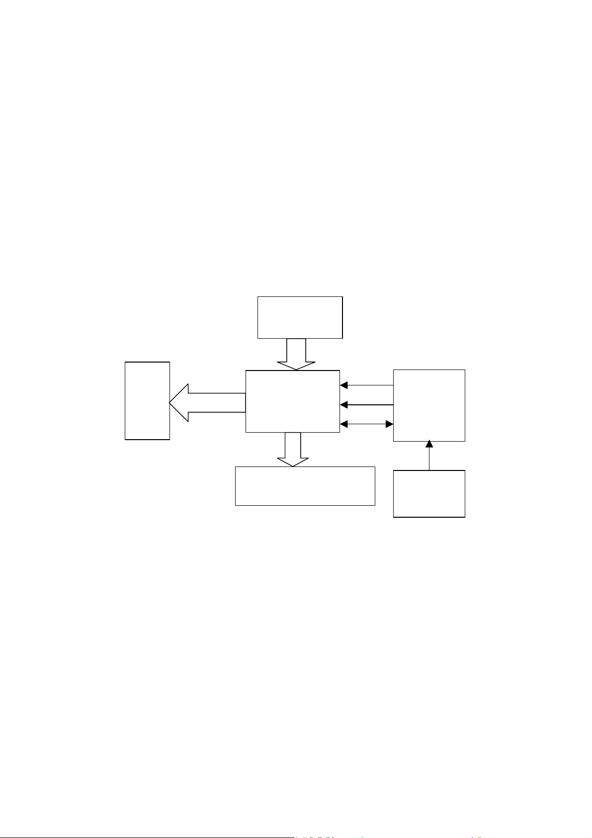
I. Components of the Complete-machine
AV310T (RU) consists of the following seven components:
1. Signal processing board: for signal gating, pre-amplifying and the pre-processing of Karaoke
signals
2. Decoding board: in charge of the control to the whole power amplifier and the digital signal
process;
3. Control Board: VFD Display, the menu button and main volume control
4. Power board and protection circuit: to supply the working voltage needed to unit circuit and
carry out the protection function to the whole power amplifier;
5. Amplifier board: to amplify the power of the 5.1-channel signal and simulated signal;
Page 2

6. Earphone board: to amplify the karaoke input and earphone output signal.
II. Signal Processing Board
1. The six input styles of AV310T (RU): Fiber input, coaxial input, CD, DVD, 5.1-channel and
radio input.
The digital signal of fiber and coaxial input is processed in decoding board through lines. The
simulate input option of AV310T (RU)is realized through the two electric switches, the truth table
is as follows:
CD4052 Truth Table
CD Radio DVD
A 1 0 1
B 1 1 0
The three simulated input status : AV310T(RU)has the three simulated input states: radio, CD,
DVD, which are controlled through signal 4052-A and 4052-B respectively(refer to the truth table).
The gated signal is output from Pin 3 and Pin 13 of N101; then through N111 CD 4052, the main
channel signals of the right and left are output through Pin1 and Pin12; the signal is finally
processed in the decoding board.
The simulated signal input in 5.1 state: The 5.1 simulated signal input of AV310T(RU)controls is
gated by the two IC CD 4053s, Pin 9, Pin 10 and Pin 11 of which is controlled by the signal 5.1CH
output from Pin 4 of M62446. When signal5.1CH becomes high level, the strobe becomes the
State5.1 simulated signal input, under which the digital sound field disappears and all the signals
becomes direct. When signal 5.1 CH becomes low level, the strobe becomes the signal composed
through decoding.
The shift control of direct mode and digital sound field mode: AV310T(RU)has direct mode and
digital sound field mode, its strobe input is controlled by N111 CD 4052 and N102 CD 4053.
When signal 4053-INT becomes high level, the IC is out of working status as it is connected to the
emarginated terminal of N102, thus the main channel signal is output through Pin 6 and Pin 11 of
N111, and directly transmitted to the hi-fi music signal processed by M62446. When 4053-INT
becomes low level, the main channel signal is transmitted to decoding board for digital sound
process, while N102 is still under working status.
2. The signal process of Karaoke
After the signal of Karaoke transmitted from M-board is amplified in coupling amplifier, it is
directly transmitted to Volume and Key Control IC PT 2315 for processing, after the reverberation
delay is adjusted in PT2399, it is transmitted through band pass filter to loudspeaker for
small-signal amplifying. As PT 2315 is controlled by CPU, the user may adjust it through the
remote controller as they like.
While the other signal, after being amplified and rectified, is used to control the switch triode
V201 9014 and in turn to control the high level and low level of the Test Signal P-KT to test
Karaoke signals. When the input Karaoke signal is strong enough to lead the direct current
rectified to triode 9014, and to lower the P-KT signal, which indicates the input of Karaoke signals.
When the system is unable to detect signals in a certain period of time, the system will
automatically becomes soundless in the section of Karaoke and prevent the outside noise from
affecting the audio effect.
3. The switch-on of fan
When the amplifier is loaded, given that the power increases and the temperature raises fast, the
Page 3

power amplifier equipped with fan for heat radiating. When volume is bigger than 45 DB, the
signal of fan becomes high level, V103 and V105 becomes electrified and forms a circuit to switch
on the fan. But when the earphone is loaded, the control line PH-SW becomes high level, then
V104 becomes electrified and lowers the signal of the fan, consequently, no matter how high the
system volume is, the fan will not be switched on.
III. Decoding Board
The main components of the decoding board are listed as follows:
CPU: the controlling core of the power amplifier
IC 493264:the high-performance digital audio decoder, including DOLBY decoding, DTS
decoding and DSP processing.
IC 8415: Serial audio digital signal receiver
IC CS5340:2-channel A/D shift
IC CS 4360:6-channel A/D shift
IC 24C02:status saving
IC 74HC04:multiplex (MPX) inverter
IC BM1117-3.3:3.3V stable voltage IC supplying power to CS8415, CS4923
Working Principle
After the fiber and coaxial signal go through the inductance filter and capacitance filter, it will be
inverted in the inverter and then transmitted to Pin 4, Pin12 and Pin 14 of the serial audio digital
signal receiver IC CS8415, through this IC, the serial audio digital signal is transformed into PCM
signal and output through Pin 16(sampling rate signal), Pin 17(main channel clock signal) and Pin
18(audio data signal) to Pin 25(sampling rate control signal), Pin 26(clock signal) and Pin
22(PCM data input interface 1) of the digital audio decoder IC CS4923, and the data will then be
processed.
After the signal of the simulated right and left channels signal is transmitted through Line XS17 to
decoding board for small-signal pre-processing , it will be transmitted to Pin 10 and Pin 12 of IC
CS5340 for A/D shift, turning the simulated audio signal into PCM signal, and then transmitted
from Pin 4(audio PCM signal), Pin 17(sampling rate signal) and Pin18(clock signal) of CS5340 to
Pin 27, 28 and 29 of CS 4923, i.e. it is transmitted to the other PCM interface of CS4923 for data
processing.
In consequence, the digital sound field processing of simulated signal and the coaxial and fiber
processing are relatively independent, if either of the processing does not work, the problem will
more probably occurs before CS4923.
CS4923 has the function of digital sound field processing, within which DSP processing, PROH
processing and DOBLY/AC-3 processing takes place through the CPU.
The audio PCM signal processed by CS 4923 is transmitted to CS4360 for D/A shift, turning the
PCM signal back to the 6-channel simulated signal, then it filters the noise beyond the frequency
range in the band pass filter, finally it is transmitted to input gating section for choice input.
As the core of the whole machine, CPU is of vital importance. Through it, all control signals
controls the actions and continuously check different signals and the user’s orders to control the
action of every part of the machine. In case the CPU is of bad quality, the whole machine will not
be able to work properly.
In addition, this machine does not have the automatic searching function; instead, it will
Page 4
automatically save and memorize the last working status and the first working status after the
n
machine being switching on.
This machine is qualified with radio function, offering the users a variety of function choices. It
receives the frequency signal through the radio head controlled directly by CPU and outputs the
signal after being amplified through power amplifier. The radio head and LM62446 share the
clock and the data line, while the other control lines are directly connected to CPU, and the L and
R signals processed by the radio head are directly transmitted to the pre-amplifier for strobe input.
Ⅳ.Control Board
The control board mainly consists of VFD display, driver IC PT6311and remote receiver
HSOO38A2 and signal lamp video circuit. It mainly assumes the task of man-computer dialogue
and working status revelation.
Diagram:
Under the control of CPU: the DST status, DCK clock and DDA data control PT6311 to show the
working status of the whole machine, in receiving the user’s orders, they control the circus of the
whole machine, enabling the whole machine to work in a designated status.
When the users operate the board buttons, the order of control is transmitted to PT6311 through
the keyboard scanning circuit; while PT6311 is driven through encoding in the inner, and outputs
the control data to CPU, which in turn control the circuit and VFD through PT6311.
VFD101is a vacuum fluorescence display screen, it is highly characterized by high light. Its
working principle is similar with the picture tube of televisions. Pin 1, 2, 46 and 47 supply power
for the filament of the bulb; CPU ultimately controls SEG polar through its control over PT6311,
enabling the characters appropriate with the working status to be revealed on the screen.
The remote receiving circuit is mainly composed by remote control receiver HS0038A2, among
which Pin 1 is connected to the ground, Pin 2 supplies the power and Pin 3 outputs the received
signals and leads them to CPU to control the appropriate circuit.
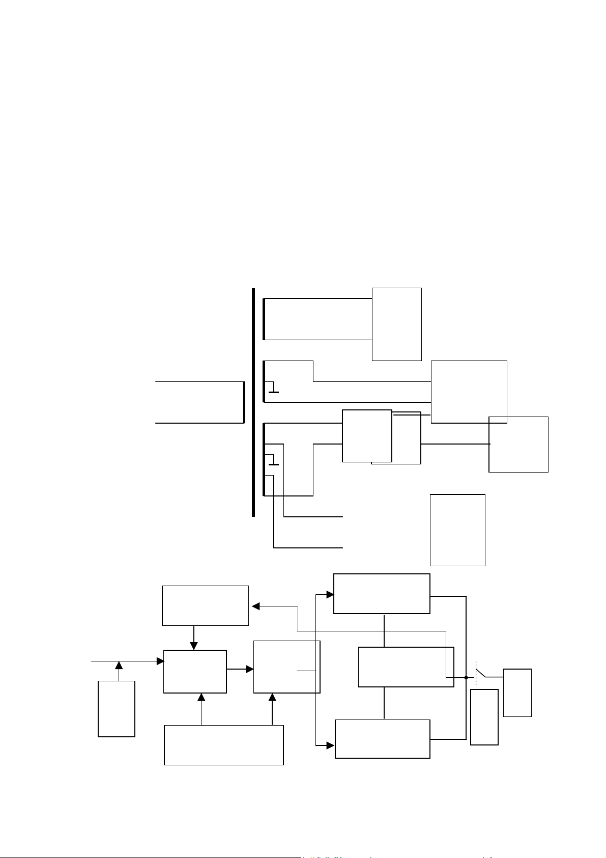
V. Po w er B oa r d
The function of power board is to supply a variety of working voltages needed by the unit circuit
VFD
Display
Control Butto
U401
PT6311
Signal Light Control Area
DDA
DCK
DST
CPU
Remote
Receiver
Page 5
of the whole machine. AV310(RU)applies a annular transformer of 335W. The Central Channel
p
r
r
r
N
r
r
r
and surround channel of AV310(RU)adopt LM1875 and LM4731 respectively, and LM4731 is
amplified IC powered by dual channels, which adopts independent positive power source to
supply electricity, enabling a high separation between the two surrounding channels; Compared
with the previous products, it adds ±VSS power supply, which is illustrated as follows:
1. The two alternating currents of 38V firstly transmitted from the transformer are filtered and
rectified through the four IN5404 and the two electrolysis condenser 15000uF/68V, and then the
±53V power is obtained for power supply of the right and left channels.
2. The two alternating currents of 21V secondly transmitted from the transformer are filtered and
rectified through the four IN5404 and the two electrolysis condenser 47000uF/35V, and then the
±28V power is obtained for power supply of Channel SL/SR/C. In addition, the other ICs and
collinear amplifier supply its IC with powers obtained through regulation from the regulator tube
L7812 and L7912.
~26V
Board
Display
Screen
~220V50HZ
~38.5
Rectifica
V
-tion
filte
R
ectifica
-tion
filte
~2.2V
Filament voltage
Dual-channe
l powe
amplifier
~16.3V
egative feedback
R121,R108,C105
compound amplifie
V132,V112
C,SL,SR
channel
ower
amplifier
L IN
V101
V115
mute
Differential
amplifier
constant current source
circusV104,V107,VD102,VD1
Voltage Ampl
stageV105
ifie
.
Temperature compensatio
stage V106
compound amplifie
stage V133,V113
Relay
Louds
oeake
r
Page 6

V. Loudspeaker Board and Protection circuit
I. Channel L and R Power Amplifying circuit: The channel L and R main loudspeaker circuit of
AV310(RU)consists of discrete components, which is shown as follows: ( e.g: Channel L)
The channel signal is transmitted through coupler R101、R103、C101 to Polar B of
differential amplifier stage V102, V102 and V103 compose the differential amplifier circuit with
one-end input and output. Sound signals are transmitted from Polar C of V102 to Polar B of
voltage amplifier V105, after the voltage is amplified; it is output to compound power amplifier.
V104, V107, VD102 and VD103 compose constant current source circuit, among which VD102
and VD103 supply stable base current to V104 and V107. The emitter resistance of V104 decides
the working current of differential amplifier stage, while the emitter resistance of V107 decides
the working current of voltage amplifier stage. V132 and V112 compose composite tube amplifier,
ensuring that the lowest-level energy of the power amplifier have sound current amplifying
capacity, and they composes positive 1/2 duty cycle amplifying. V133 and V113 compose the
negative duty cycle amplifying,the circuit construction is completely same with that of the upper
tube. Temperature compensation tube V106 has two functions in the circuit: first, it is the base bias
of the upper and lower tubes, its working status decides the stable working current of the
compound amplifier stage, i.e. by adjusting the electric conduction degree of V106, we can set the
static working point of compound amplifier stage , while the common method is to change the
base resistance of V107; it also automatically adjust the working status of the compound amplifier
stage after the temperature rises. The adjustment process is specified as follows:
Total current of output stage= working current +leakage current
When the temperature rises, the leakage current increases and leads to the floating of static
working point, which is harmful.
Meanwhile, the leakage current of V106 increases, Uce decreases and in turn to decrease the
bias-current of output stage, changing the working status and decreasing the working current of
back-end amplifier, as a result, realizes temperature compensation.
In the power amplifying circuit of AV310(RU), the negative feedback of voltage is
induced, which is composed of R121, R109 and C105, and is used to stabilize the static working
point of differentiate stage. AV310(RU)adopts direct output method, R111 and C116 connected
with the output end form Roberl Network which prevents the high-frequency self-oscillation
resulted from alternating current inductance in the loudspeaker voice coil.
2. Working principle of Channel R: (refer to the working principle of Channel L)
3.Mute circuit: When you press the button “Mute”, the remote control receiver transforms the
signal into a signal of “mute” to CPU, form which Pin 35 and 36 send out an order of “high level
mute” electrifying V115, V101 and V116, the left and right channels short-circuited the signal to
the ground, consequently complete the function of mute control.
The Power Amplifying circuit of C, SR and Sl: Compared with the machine in the past, the three
channels of AV310(RU)adopts the exclusive power amplifier LM4731 and IC LM1875. LM4731
has 15 pins, among which Pin 2, 15 and 4 are its negative and positive power pins respectively,
while Pin 7, 8, 12 and 13 are its in-phase input and out-phase input, the fixed output wattage of the
IC with such wattage may reach 20 W and makes it possible for becoming automatic mute when
the machine is on; while 1875 is a high-performance power amplifying IC with 5 pins, its
application circuit is simple and has an output wattage of 15 W in fixed status. Pin 5 and 3 are the
power-supplying pins of positive and negative electrics.
Page 7

5. Protection circuit
f
The channel L, R and C is protected by switching off relay Y100 to switch off the output. Channel
SR and SL are protected through the use of “mute” function. AV310(RU)has the protection mode
of delay-on-start ,over-pressure and over-flow protection and idle protection.
1) Delay-on-start protection circuit: since the circuit is unstable when the machine is turned on, the
impulse current resulted will do great harm to the loudspeaker and wattage amplifying circuit, thus
a delay-on-start protection circuit is established. The delay-on-start protection circuit works in two
steps: first, C, L and R. The working process is as follows: the alternating current output from
transformer is filtered and rectified in VD113 and C110, and sends out a voltage of 22V to
recharge C115 through R108, producing a reverse cutout on VD111 and in turn electrify V105 and
V104, ultimately magnetifies Y100 and achieves the delay. Second, the right and left sound
channels protects the machine from impulse current in the way as follows: when the system of the
machine restores itself, Pin 22 of CPU outputs a high level through R164 to Pin 9 and 14 of
LM4731, enabling LM4731 to output mute; when the delay-on-start begins, Pin 33 of CPU
immediately turns into low level to ensure path SL/SR to be output in normal way.
Over-pressure protection: An over-pressure sampling resistance is connected with the output of
each channel; R116 is connected with Channel L, R117 with Channel R, R118 with Channel C,
and R119 and R120 with SR and SL respectively. In case the voltage of either of the channels
surpass +3.5V or lower than-3.5V, either V101 or V102 is electrified and enables the voltage of
Polar C to step down, in turn V103 is electrified and helps switch off the Relay and switch on the
Protection circuit.
Over-pressure
sampling resistance
linked to channels
﹥+3.5V
R116
with L
﹤+3.5V
V101 ON
V102 ON
Voltage
of Polar
C ↓
V103
ON
Relay OFF,
Protection ON
2. Short- circuit protection: Each output port of Channel L and R is respectively linked with an
over-flowing sampling resistance, the sampling tube of Channel L is V114, the loading resistance
is R126 and R127. The other three channel power amplifying IC possesses over-flowing function
within itself. When over-flowing occurs in Channel C, the step-down of voltage on R126 and
R127 will promptly increases, in case the step-down of voltage on R129 is over than 0.7V, V114 is
turned on, in turn V103 is turned on, and ultimately the Relay will be turned off to start the
protection circuit.
Over-flowing
Sampling troid is
connected with
each channel
V114
withCha
nnelL
When overflow,
R126&R127step
-down↑
V114
ON
Voltage o
PolarC↓
V103
ON
Similarly, when over-flowing occurs in Channel R, the voltage of R159 is over than 0.7V, V129 is
thus turned on , in turn V103 is turned on, ultimately the Relay will be turned off to protect the
RelayOFF,
Protection ON
Page 8

loudspeaker.
Appendix
Appendix I.
F
更 改 数 量 更改单号 签 名 日 期
设 计 审 核
1
23
标 准 化
批 准
AV310TÔ-Àí¿òͼ
4
第 张 共 张
东莞市步步高视听电子工业有限公司
BBK
5
版次:
6
F
DIGITAL AUDIO INPUT
КэЧЦТфЖµ
TUNER
CD
L
DVD
R
L
5.1CH
R
9
8
7
6
5
4
3
2
1
MIC¡¢PHONE BOARD
1
2
3
1
2
3
L/R
L/R
5.1CH(L/R/SL/SR/C/SW)
+5V
PH_SW
PH_L
PH_R
4052_A /4052_B
4052*2
OK_CLK/OK_DATA
E
2*COAXIAL/OPTICAL
L/R
DO/CLK/DAT/CE
P_KT
¼ì²â
4558_B
·Å´ó
4558_A
·Å´ó
·Å´ó
LM4880
E
PT2315
MIC_VOL
TONE
ECHOµ÷½Ú
P_RLY
Ë«½âÂë°å
Ë«½âÂëIC,CPU
P_DISP
CPU
P_RLY
»ìÉÎ
PT2399
CPU I/O :
D
5.1CH
4053_INT
L/R/SL/SR/C/SW
0_LEVEL
STEREO INPUT
REMOTE
VOL&TONE
CLK / DAT/ LAT
2*KEY
VFD
FAN
FUN VOLTUN_L/TUN_R
REMOTE
6311 I/O :
62446 I/O :
M62446
INPUTSET
4053*2
DISPLAY BOARD
2*LED
PT6311
DCL/DDA/DST
»ìºÏ&»º³å
ֱͨ
4558
»ìÉÎÁ¿
CLK/DATA/LAT
DO/CE
OK_CLK/OK_DATA FAN
P_KT
DCL/DDA/DST
REMOTE
P_LRM/P_SCM
P_RLY
P_DISP
KM
D
C
SW
KM
FAN
TUN_L/TUN_R
4052_A /4052_B
5.1CH 4053_INT
C
SL/SR
L/R
C
OK_L/R
OK_C
+12V
AGND
-12V
~VS
RLYC
Diagram 1.Working Principle Diagram
»ìºÏ&»º³å
4558
»ìºÏ&»º³å
5532
»ìºÏ&»º³å
4558
±6.8V
B
A
1
P_LRM/P_SCM
AMP BOARD
+12V
-12V
AGND
功
L
R
C
SL
SR
Vs+ GND Vs-
继
电
器
¼МµзЖчЗэ¶¯
RLYC
主功放电源
POWER BOARD
前置
电源
中环
电源
SW¾²ÒôºÍ¼ÌµçÆ÷״̬¼ì²â
2
3
L
R
45
C
SL
SR
率
放
大
MUTE
过载
SW_OUT
SWM
+6.8V
电源
AGND
-6.8V
+5V~VS
+5V
+5VD
检测
保
护
电
路
Vc+
AGND
Vc-
6
B
A
F
更 改 数 量 更改单号 签 名 日 期
设 计 审 核
1
23
标 准 化
批 准
AV310TÐźŰåÔ-Àíͼ£¨Ò»£©
4
第 张 共 张
东莞市步步高视听电子工业有限公司
BBK
5
版次:
6
F
TUNER_L
TUNER_R
COAX1
COAX2
OPTICAL
DVD
CD
XC103:1
XC103:2
XC103:3
E
V106
XS20
CE
11
DATA
R
L
R
L
R
L
OUTPUT
9
8
7
6
5
4
3
2
1
R
L
R
L
R
L
C101
CLK
47n
DO
R101 1K
R102 47K
R103 47K
R104 1K
R105 1K
9
R106 47K
8
R107 47K
7
R108 1K
R109 1K
6
R110 47K
5
R111 47K
4
R112 1K
3
2
C171
104
1
C105
47u/16V
1
VCC
2
GND
R152
C106
3
104
75
L101
47uH
C109 104
VD5
RX3
RX2
DGND
RX1
AGND
AGND
1
2
3
4
5
6
7
8
9
-12V
10
+12V
R115 1K
3
R116 47K
2
R117 47K
1
R118 1K
R119 1K
6
R120 47K
5
R121 47K
4
R122 1K
R123 1K
9
R124 47K
8
R125 47K
7
R126 1K
10
9
8
7
6
5
4
3
2
1
CON11
XC101:3
XC101:2
XC101:1
XC102
RX178B
XP17
CON9
XP16
CON10
From Audio Decoder
SR
SW
SL
AGND
FR
C
FL
AGND
-12V
+12V
R
L
SR
SL
SW
C
S8050
C102
47u/16V
VD112
10V
C108
10u/16V
C107
10u/16V
5.1CH
E
TUNER_R
D
+12V
L102 47uH
R139 1K
C110
10u/16V
N101
CD4052
12
X0
14
13
X1
X
15
DVD-R
X2
11
CD-R
X3
3
Y
1
Y0
5
TUNER_L
Y1
2
DVD-L
Y2
4
CD-L
4052_B
4052_A
5.1CH
16
Y3
VDD
A+6.8V
6
INH
8
VSS
9
B
B
7
VEE
A-6.8V 4052_B
10
A
A
N111
CD4052
12
X0
14
13
X1
X
15
X2
11
X3
3
Y
1
Y0
5
Y1
2
Y2
4
16
Y3
VDD
A+6.8V
6
INH
8
VSS
9
B
B
7
VEE
A-6.8V
10
A
A
INT
R149 4K7
R150 4K7
N102
CD4053
12
14
FR
X0
X
13
X1
2
15
FL
Y0
Y
1
Y1
5
4
C
Z0
Z
3
Z1
16
VDD
A+6.8V
6
INH
11
8
A
Vss
10
B
7
C9VEE
A-6.8V
N103
CD4053
12
14
SR
X0
X
13
X1
2
15
SL
Y0
Y
1
Y1
5
4
SW
Z0
Z
3
Z1
16
VDD
A+6.8V
6
INH
11
8
A
Vss
10
B
7
C9VEE
A-6.8V
D
Diagram2. Signal Processing Board 1
4053_INT
C
R130
100K
R131
100K
R129
470K
R132
470K
R133
470K
R128
470K
R168 470K
N105:2
6
C153
7
5
4.7u/16V
4558
R136
R135
R134
R127
22K
22K
22K
22K
1
A
4052_A
C109
47n
A+6.8V
4053_INT
5.1CH
C110
47u/16V
B
INT
5.1CH
2
3
4
5
6
C112
4.7u/16V
7
8
C115
4.7u/16V
9
C117
4.7u/16V
10
11
C120
4.7u/16V
12
13
C122
4.7u/16V
14
15
C124
4.7u/16V
16
17
C126
18
822
19
C127
15n
20
C128
0.33u
A-6.8V A+6.8V
C129
C131 47n
47u/16V
C
+12V
R183
470K
R185
R170
680
47K
OUT4
OUT3
OUT2
OUT1
AVDD
SWIN
N104
GNDS
SWOUT
M62446
SRIN
SLIN
GNDC
CIN
GNDR
RIN
GNDL
LIN
BYPASR
BYPASL
LTRE
LBASS3
RBASS3
LBASS2
RBASS2
LBASS121RBASS1
-12V
R137
220/0.5W
VD101
6.8V
C132 47n
47u/16V
B
+12V-12V
R184
N105:1
47n
C123
C125
220/0.5W
42
41
40
39
38
37
36
35
34
33
32
31
30
29
28
27
26
25
24
23
22
R138
VD102
6.8V
8 4
+12V
C113 4.7u/16V
C114 4.7u/16V
C116 4.7u/16V
C118 4.7u/16V
C119 10u/16V
C121 10u/16V
4558
C137 47n
C140
C141
20K
VD110
VD111
1
1N4148
1N4148
C170
10u/16V
-12V
C133
47u/16V
L103 100uH
C134
C135
101
101
A-6.8V
C138
47u/16V
C139
822
15n
0.33u
+12V
2
3
C111
DVDD
CLK
DATA
LATCH
DGND
AGND
SROUT
SLOUT
COUT
ROUT
LOUT
AVSS
CL1
4.7u/16V
CL2
CR1
4.7u/16V
CR2
RTRE
+12V
C130
B
A
1
P_DISP
R186
10K
+5VD
CLK
CLK
DATA
DATA
R141 100
LAT
LAT
SW-1
SW-1
SR-1
SR-1
SL-1
SL-1
C-1
C-1
R-1
R-1
L-1
L-1
2
3
45
XS6
-12V
4-12V
DGND
3
DGND
2
+12V
1
CON4
A
6
Page 9

F
更 改 数 量 更改单号 签 名 日 期
设 计 审 核
1
E
D
C
B
A
1
23
标 准 化
批 准
AV310TÐźŰåÔ-Àíͼ£¨Èý£©
4
第 张 共 张
东莞市步步高视听电子工业有限公司
BBK
5
版次:
6
F
F
更 改 数 量 更改单号 签 名 日 期
设 计 审 核
1
XS12
P_RLY
1
+5V
2
DGND
3
L-1
4
R-1
5
PH_SW
6
GND
7
MIC
8
CON8
SW-1
SW-1
C-1
C-1
L-1
L-1
R-1
R-1
SL-1
SL-1
SR-1
SR-1
OK
OK
V101
2N5401
R142
KM
KM
4.7K
R160
C148
XP14
7
6
5
4
3
2
1
CON7
PH_SW
P_LRM
P_SCM
XS21
1
2
3
CON3
FAN
PH_SW
XS11
1
2
3
CON3
10K
22u/16V
PH_SW
KM
P_RLY
P_LRM
P_SCM
+5VD
VD103
PH_SW
1N4148
VD104
1N4148
VD105
P_LRM
1N4148
VD106
P_SCM
1N4148
R164
10K
R143
FAN
4.7K
R144
V104
PH_SW
9014
4.7K
VD108 1N4004
R145 1
C103
104
R146 1
VD109 1N4004
E
R147 15K
R155
47K
R158
100K
V102
S8050
C149
4.7u/16V
LRM
LRM
SCM
SCM
R165
10K
VD107
1N4148
V103
9014
V105
S8050
R167
1/0.5W
C151
C150
104
2200u/16V
D
R171 47K
R173 22K
8 4
R175 33K
8 4
R181 22K
8 4
R172 1K
C15510u/ 16V
N106:2
5532
7
-12V
N106:1
5532
1
C1
C15710u/ 16V
+12V
L1
C15910u/ 16V
N107:2
5532
7
R1
-12V
C16110u/ 16V
N107:1
5532
1
+12V
R188 100
SL1
N108:2
5532
7
-12V
N108:1
R189 100
5532
1
SR1
+12V
R148 10K
C154 103
C146
6
103
5
C156 47P
R156 20K
2
R174
3
47K
C158 47P
R157 20K
C147
4.7u/16V
R159 15K
6
R176
5
47K
C160 47P
R161 20K
R177 33K
R162 15K
2
R178
3
47K
C162 47P
R179 22K
R163 20K
6
R180
5
47K
C164 47P
R166 20K
2
R182
3
47K
C
Diagram3. Signal Processing Board 2
E
D
C
N109
AMS1085-5
3
Vin
LINE OUT
1
R187
47K
SWM
L1
R1
C1
SL1
SR1
P_RLY
P_RLY
RLYC
RLYC
LRM
LRM
SCM
SCM
+12V +12V
C166
47u/16V
C168
47u/16V
C176
103
1
GND
Vout
C173
1000u/16V
2
B
B
XC104
SW-OUT
2
2
XS9
1
2
3
4
5
6
7
CON7
XS13
From AMP Board
1
2
3
4
5
CON5
C167
104
C169
104
-12V-12V
C175
104
+5VD
3
45
6
A
A
1
23
标 准 化
批 准
AV310TÐźŰåÔ-Àíͼ£¨¶þ£©
4
第 张 共 张
东莞市步步高视听电子工业有限公司
BBK
5
版次:
6
F
+12V
C210 47u/16V
R205
100/0.25W
VD201
9.1V
C201 151
C215
100u/16V
C202 4.7u/16V
R201 33K
R202 4.7K
N201:2
4558
6
7
5
R203
1K
C204
10u/16V
C205 10P
R204 100K
-12V
N201:1
4558
2
1
3
8 4
+12V
C203
MIC
MIC
4.7u/16V
XP18
CON13
LAT
1
CE
2
CLK
3
DATA
4
DO
5
P_DIST
6
OK_DAT
OK_DAT
7
OK_CLK
OK_CLK
8
P_KT
P_KT
9
Remote
10
DST
11
DCK
12
DDA
13
XS15
+5VD
1
2
RLYC
3
NC
4
DDA
5
DCK
6
DST
7
FAN
8
REMOTE
9
CON9
E
N203 PT2315
1
20
OK_CLK
REF
CLK
2
19
VDD
DATA
3
18
AGND
C211
47n
VD202
1N4148
DGND
C212
4
17
TREBL
LOUT
5.6n
C213
5
16
TREBR
ROUT
6
RIN
7
LOUD_R
8
NC
9
LOUD_L
NC10LIN
4.7u/16V
15
BOUT_R
14
BIN_R
13
BOUT_L
12
BIN_L
11
P_KT
C219
V201
103
9014
R207
47K
5.6n
R206 1K
C220
47u/16V
D
OK_CLK
OK_DAT
OK_DAT
C214
C216
68n
C217
68n
R210
5.6K
C218
4.7u/16V
P_KT
N202:2
4558
6
7
5
C
Diagram4. Signal Processing Board 3
4.7u/16V
+12V
C224
4.7u/16V
C230
R224
10K
C233
5.6n
N204
PT2399
C242
47n
R234
220/0.5W
VD203
B
R219 47K
R218 20K
R220 10K
C226
101
-12v
N202:1
2
1
3
4558
8 4
+12v
R222
4.7K
C227
103
C228
R225
4.7u/16V
22K
R226
2.7K
C229
R227
C231
2.7K
103
4.7u/16V
C232
5.6n
12K
15K
10K
10K
R228
R230
R231
R23215K
R229
C236
C234
C235
0.1u
681
681
11
12
13
15
16
F2-I
F1-I
P2-O
F2-O14F1-O
VCC1REF2AG3DG4CLK5VCO6CC17CC0
C238
R233
20K
47u/16V
C240
C241
103
C243
47u/16V
5.1V
2
C244
R221 1K
OK
OK
4.7u/16V
3
C237
0.1u
9
P1-I10P2-I
P1-O
8
C239
0.22u
0.22u
45
6
A
Page 10

F
更 改 数 量 更改单号 签 名 日 期
设 计 审 核
1
23
标 准 化
批 准
½âÂë°åÔ-ͼ(Ò»)
2310TA-1
4
第 张 共 张
东莞市步步高视听电子工业有限公司
BBK
5
版次:
6
F
E
C157
1U/16V
L107
VD2.5
49326_DI
49326_CK
49326_CS
49326_DO
INT_49
DSPRST
SDA
SCK
DARST
9
RR105
8*3.3K
8415_ERR
8415_INT
XTAL2
G101
C103
12.288MHz
30P
R101
1M
C101
104
R102 51
N101:3
5 6
74HC04
N101:5
11 10
74HC04
C159
FB
104
C203
30P
N105
CS49326-3
7
8
C202
9
30P
10
11
12
13
C109
14
104
15
16
17
R109
R113
51
51
C110
104
R114 51
VD3.3
C205
R112 51
30P
R154 470
R153
51
1 2 3 4 5 6 7 8
R152 51
R151 51
R118
10K
R150 51
L101
VD5
FB
C112
C113
1U/16V
104
C114
472
C115
104
VD3.3
VD5
X01
L121
1UH
1 2
N101:2
3 4
74HC04
X02
L122
1UH
R103 51
R104 51
C105
104
147
N101:1
74HC04
XTAL1
C104
30P
E
C108
104
R105
R108
4K7
4K7
MCLK
6
5
4
2
1
44
3
DIN
VD1
EMOE
EMWR
DGND1
SCK
XMT958
GPIO7
GPIO6
GPIO5
GPIO4
CS4923
VD2
DGND2
GPIO3
GPIO2
GPIO1
GPIO0
/CS18DOUT19/INT20EXTMEM21SDATAN22VD323DGND324BCK125WCK126CMPDAT
DIN2
R111
10K
R155
C206
51
30P
1
SDA SCK
SDA/CDOUT
2
AD0/CS
3
EMPH
4
RXP0
5
C111
RXN0
104
6
VA+
7
AGND
8
FILT
9
RST
10
R119
RMCK
11
1.2K
RERR
12
RXP1
13
RXP2
RXP314RXP4
R162
N106
470
104
104
104
C207
C208
C209
75
101
R11675R117
C218 101
C215 101
C219
75
R115
MCLK
SCLK
43
BCK
SCLK2
C204
30P
L117
1UH
L119
1UH
D
R106 51
R107
R110
SDIN2
LRCK
SDIN1
42
41
40
AD0
WCK
/RESET
CLKSEL
CLKIN
27
28
DIN1
SCLK1
LRCK2
SCL/CCLK
AD1/CDIN
DGND
OMCK
SDOUT
OLRCK
OSCLK
CS8415ASO
D
51
51
R120
10K
SDIN3
AD1
39
AD2
38
DC
37
DD
36
35
AGND
34
VAA
33
FILT1
32
FILT2
31
30
29
LR2
R123
10K
BCK2
LRCK1
28
27
26
RXP6
25
RXP5
24
H/S
23
VD+
22
21
20
U
19
INT
18
DIN2
17
16
15
C210
104
R164
X02
470
N101:4
74HC04
C214
98
104
R179
750
R178
47K
R182
0
N101:6
C217
1312
104
750
74HC04
R181
47K
R180
R183
0
Diagram 5. Control Board
C120
471
LRCK2
101
C216
R121
10K
C117
2.2U/16V
R122
33K
C119
103
SCLK2
X01
L116
1UH
C213
101
L120
1UH
L118
1UH
Rin
123456789
XS17
CON9
L104
FB
VD2.5
C121
104
Lin
DIGITAL INPUT
C
R161
51
C116
1U/16V
C118
104
VD3.3
R156
51
R159
VD3.3
L114
1U/16V
FB
VD3.3
L102
FB
C135
1U/16V
C129
VD5 +12V VA5
100U/16V
C130
104
L103
+5VD
RX1
RX2
RX3
VD5
P14
P15
P16
P17
1234567
KM
P_RLYC
P_LRM
P_SCM
N107
CS4360
1
VLS
MUTEC1
2
SDIN1
AOUTA1
3
SDIN2
AOUTB1
4
SDIN3
MUTEC2
SCLK
5
SCLK
AOUTA2
6
LRCK
LRCK
AOUTB2
7
MCLK
MCLK
VA
8
VD
AGND
9
GND
AOUTA3
10
DARST
/RST
AOUTB3
11
SCK
DIF1
MUTEC3
12
SDA
DIF0
VQ
13
M1
FILT+
VLC14M2
L105
C123
1U/16V
FB
VD5
C124
104
L106
C125
1U/16V
FB
VD3.3
C126
104
L113
C155
1U/16V
FB
N108
1
C127
M0
104
10K
C128
C106
104
N109
BM1117-3.3
3
Vin
N110
BM1117-2.5
3
Vin
PH_SW
XS14
CON7
M1
2
MCLK
FILT+
3
VL
REF_GND
4
DIN1
SDOUT
VA
5
GND
AINR
6
VD
VQ
7
SCLK1
SCLK
AINL
LRCK1
LRCK8RST
CS5340
VD3.3
2
Vout
GND
C131
100U/16V
1
VD2.5
2
Vout
GND
C134
1
100U/16V
VD103 1N4004
PH_SW
C
B
A
1
28
27
26
25
24
23
22
21
20
19
18
17
16
15
C156
104
16
15
14
13
12
11
10
9
C154
104
C158
104
DA_L
DA_L
DA_R
DA_R
DA_SL
DA_SL
DA_SR
DA_SR
DA_C
DA_C
DA_SW
DA_SW
L111
C146
104
FB
104
1u/16V
104
1u/16V
C143
C145
C144
C122
R165
0Ohm
C150
104
C153
104
R157
2.2K
C161
C107
104
10U/16V
VA5
C147
1u/16V
L112
C149
VA5
C148
1U/16V
FB
1U/16V
C151
104
Ain-R
Ain-R
C152
1U/16V
Ain-L
Ain-L
V102
5551
R158
C136
100K
VD102
5.6V
104
C133
47U/16V
C132
10U/16V
VA5VD5
163
R
0Ohm
2
3
45
VD2.5VD3.3
6
B
A
F
更 改 数 量 更改单号 签 名 日 期
设 计 审 核
1
23
标 准 化
批 准
½âÂë°åÔ-ͼ(¶þ)
2310TB-1
4
第 张 共 张
东莞市步步高视听电子工业有限公司
BBK
5
版次:
6
F
OK_DAT
OK_CLK
E
D
C
B
A
1
N115
24C04
+5VD
V101
9015
RR102
8*4.7K
1 2 3 4 5 6 7 8
+5V
XS18
CON13
P10
1
LAT
P11
R
2
CE
P12
R
3
CLK
P13
R
4
DATA
P30
R
5
DO
P31
6
P_DIST
R170
7
R
8
P34
9
P_KT
P35
10
Remote
P36
11
DST
P37
12
DCK
P25
13
DDA
P_SCM
P14
P_LRM
P15
VD101
P_RLYC
P16
470
166
470
167
470
168
470
169
P27
470
P26
470
171
1N4148
KM
P17
R172
470
8415_INT
INT_49
+5V
1 2 3 4 5 6 7 8
RR103
8*4.7K
R127
22K
Rin
Rin
Lin
Lin
6
5
R128
100K
R129
10K
R130
2
22K
3
R131
100K
E
R125
C163
5K6
104
C164
-12V
+12V
7
C168
104
1
C170
104
1
2
3
4
5
6
7
8
9
10
11
12
13
14
15
16
17
18
19
PGND
10U/16V
PGND
N116
P10(T2)
P11(T2)
P12
P13
P14
P15
P16
P17
RST/VPD
P30(RXD)
P31(TXD)
P32(INT0)
P33(INT1)
P34(T0)
P35(T1)
P36(WR)
P37(RD)
XTAL2
XTAL1
VSS20P20(A8)
P89C238MBP/B
C166
Ain-R
10U/16V
C169
Ain-L
10U/16V
9
9
R126
10K
C165
331
N111:2
5532
C167
331
N111:1
5532
8 4
D
L108
FB
R124
C162
VD101
10K
104
1N4148
C172
47U/16V
R173
470
40
+5V
VCC
39
P00(AD0)
38
P01(AD1)
37
P02(AD2)
36
P03(AD3)
35
P04(AD4)
34
P05(AD5)
33
P06(AD6)
32
P07(AD7)
31
/EA(VPP)
30
ALE
29
/PSEN
28
P27(A15)
27
P26(A14)
26
P25(A13)
25
P24(A12)
24
P23(A11)
23
P22(A10)
22
P21(A9)
21
+5V
1 2 3 4 5 6 7 8
RR104
8*4.7K
Ain-R
Ain-L
3
4
VSS
SDA5SCL6TEST7VDD
R174
470
49326_DO
DSPRST
SDA
SCK
DARST
49326_DI
49326_CK
49326_CS
8415_ERR
9
PGND
A01A12A2
8
P27
P26
P25
XTAL1
XTAL2
C175
DA_SL
C171
DA_SL
104
10U/16V
+5V
C178
DA_SR
DA_SR
10U/16V
C181
R139
DA_SW
DA_SW
22K
10U/16V
C184
R142
DA_C
DA_C
5.6K
10U/16V
C187
R145
DA_R
DA_R
5.6K
10U/16V
C190
R148
DA_L
DA_L
5.6K
10U/16V
C
R132
10K
C174
R133
5.6K
R136
5.6K
471
R134
6
7
3.9K
5
C176
272
R137
3.9K
2
3
C179
272
R140
6
10K
5
C182
104
R143
2
3.9K
3
C185
272
R146
6
3.9K
5
C188
272
R149
2
3.9K
3
C191
272
B
C137
10U/16V
N112:2
5532
R135
10K
C177
-12V
471
C192
104
1
C138
10U/16V
N112:1
5532
8 4
C193
104
+12V
R138
47K
C180
153
C139
10U/16V
7
N113:2
5532
R141
10K
C183
-12V
471
C194
104
1
C140
10U/16V
N113:1
5532
8 4
C195
104
+12V
R144
10K
C186
471
C141
7
10U/16V
N114:2
5532
R147
10K
C189
-12V
471
C200
104
1
C142
10U/16V
N114:1
5532
8 4
C201
104
+12V
C197
104
XS16
CON10
SR
1
SW
2
SL
3
AGND
4
FR
5
C
6
FL
7
AGND
8
9
10
L110FBL109
C198
C199
47U/16V
47U/16V
FB
A
C196
104
+12V-12V
2
3
45
6
Diagram6. Decoding Board 1
Page 11

F
更 改 数 量 更改单号 签 名 日 期
设 计 审 核
1
23
标 准 化
批 准
½âÂë°åÔ-ͼ(Ò»)
2310TA-1
4
第 张 共 张
东莞市步步高视听电子工业有限公司
BBK
5
版次:
6
F
E
C157
1U/16V
L107
VD2.5
49326_DI
49326_CK
49326_CS
49326_DO
INT_49
DSPRST
SDA
SCK
DARST
9
RR105
8*3.3K
8415_ERR
8415_INT
XTAL2
G101
C103
12.288MHz
30P
R101
1M
C101
104
R102 51
N101:3
5 6
74HC04
N101:5
11 10
74HC04
C159
FB
104
C203
30P
N105
CS49326-3
7
8
C202
9
30P
10
11
12
13
C109
14
104
15
16
17
R109
R113
51
51
C110
104
R114 51
VD3.3
C205
R112 51
30P
R154 470
R153
51
1 2 3 4 5 6 7 8
R152 51
R151 51
R118
10K
R150 51
L101
VD5
FB
C112
C113
1U/16V
104
C114
472
C115
104
VD3.3
VD5
X01
L121
1UH
1 2
N101:2
3 4
74HC04
X02
L122
1UH
R103 51
R104 51
C105
104
147
N101:1
74HC04
XTAL1
C104
30P
E
C108
104
R105
R108
4K7
4K7
MCLK
6
5
4
2
1
44
3
DIN
VD1
EMOE
EMWR
DGND1
SCK
XMT958
GPIO7
GPIO6
GPIO5
GPIO4
CS4923
VD2
DGND2
GPIO3
GPIO2
GPIO1
GPIO0
/CS18DOUT19/INT20EXTMEM21SDATAN22VD323DGND324BCK125WCK126CMPDAT
DIN2
R111
10K
R155
C206
51
30P
1
SDA SCK
SDA/CDOUT
2
AD0/CS
3
EMPH
4
RXP0
5
C111
RXN0
104
6
VA+
7
AGND
8
FILT
9
RST
10
R119
RMCK
11
1.2K
RERR
12
RXP1
13
RXP2
RXP314RXP4
R162
N106
470
104
104
104
C207
C208
C209
75
101
R11675R117
C218 101
C215 101
C219
75
R115
MCLK
SCLK
43
BCK
SCLK2
C204
30P
L117
1UH
L119
1UH
D
R106 51
R107
R110
SDIN2
LRCK
SDIN1
42
41
40
AD0
WCK
/RESET
CLKSEL
CLKIN
27
28
DIN1
SCLK1
LRCK2
SCL/CCLK
AD1/CDIN
DGND
OMCK
SDOUT
OLRCK
OSCLK
CS8415ASO
D
51
51
R120
R121
10K
10K
SDIN3
AD1
39
AD2
38
DC
37
DD
36
35
AGND
34
VAA
33
FILT1
FILT2
LR2
BCK2
RXP6
RXP5
H/S
VD+
INT
N101:4
74HC04
R179
47K
N101:6
74HC04
R181
47K
R183
0
C117
32
31
2.2U/16V
30
29
28
27
26
25
24
23
22
21
20
U
19
18
17
16
15
C210
104
R164
470
98
R182
0
1312
C118
104
L104
R122
R123
FB
33K
10K
LRCK1
C119
VD2.5
103
C120
471
C121
104
C135
1U/16V
DIN2
SCLK2
LRCK2
X01
X02
L116
C214
1UH
104
C213
750
101
R178
L120
1UH
L118
C217
1UH
104
750
RX1
101
Lin
Rin
R180
C216
123456789
XS17
DIGITAL INPUT
CON9
Diagram 7. Decoding Board 2
C
R161
51
C116
1U/16V
VD3.3
R156
51
R159
VD3.3
L114
1U/16V
FB
VD3.3
L102
FB
C129
VD5 +12V VA5
100U/16V
C130
104
L103
+5VD
RX2
RX3
VD5
P14
P15
P16
P17
1234567
KM
P_RLYC
P_LRM
P_SCM
N107
CS4360
1
28
VLS
MUTEC1
2
27
SDIN1
AOUTA1
3
26
SDIN2
AOUTB1
4
25
SDIN3
MUTEC2
SCLK
5
24
SCLK
AOUTA2
6
7
8
9
10
11
12
13
L105
FB
L106
FB
1
2
3
4
5
6
7
GND
1
GND
1
LRCK
MCLK
VD
GND
/RST
DIF1
DIF0
M1
VLC14M2
VD5
VD3.3
N108
M0
MCLK
VL
SDOUT
GND
VD
SCLK
LRCK8RST
CS5340
2
Vout
C131
100U/16V
2
Vout
C134
100U/16V
VD103 1N4004
AOUTB2
AOUTA3
AOUTB3
MUTEC3
REF_GND
23
22
VA
21
AGND
20
19
18
17
VQ
16
FILT+
15
C156
104
16
M1
15
FILT+
14
13
VA
12
AINR
11
VQ
10
AINL
9
VD3.3
C154
104
VD2.5
C158
104
VD2.5VD3.3
LRCK
MCLK
DARST
SCK
SDA
C123
1U/16V
C124
104
C125
1U/16V
C126
104
L113
C155
1U/16V
FB
C127
104
10K
DIN1
C128
C106
104
SCLK1
LRCK1
N109
BM1117-3.3
3
Vin
N110
BM1117-2.5
3
Vin
PH_SW
XS14
CON7
PH_SW
C
B
A
1
DA_L
DA_L
DA_R
DA_R
DA_SL
DA_SL
DA_SR
DA_SR
DA_C
DA_C
DA_SW
DA_SW
L111
C146
104
FB
104
1u/16V
104
1u/16V
C143
C145
C144
C122
R165
0Ohm
C150
104
C153
104
R157
2.2K
C161
C107
104
10U/16V
VA5
C147
1u/16V
L112
C149
VA5
C148
1U/16V
FB
1U/16V
C151
104
Ain-R
Ain-R
C152
1U/16V
Ain-L
Ain-L
V102
5551
R158
C136
100K
VD102
5.6V
104
C133
47U/16V
C132
10U/16V
VA5VD5
163
R
0Ohm
2
3
45
6
B
A
F
更 改 数 量 更改单号 签 名 日 期
设 计 审 核
1
23
标 准 化
批 准
AV310TÃæ¿Ø°å
4
第 张 共 张
东莞市步步高视听电子工业有限公司
BBK
5
版次:
6
F
VD101
1N4148
XP9
SWM
1
L1
2
R1
3
C1
4
SL1
5
SR1
6
GND
7
CON7
XP13
GND
1
P_Rly
2
P_RC
3
P_LRM
4
P_CSM
5
CON5
Vs+
R163
10K
R165
4.7K
R166
4.7K
E
C101
R103
R101
1K
10K
10u/16V
V101
S8050
R161
4.7K
V115
2N5401
R162
C121
10K
22u/16V
S8050
R164
33K
C124
R167
4.7K
10u/16V
V131
S8050
V130
2N5401
R168
C122
10K
22u/16V
C123
22u/16V
R104
R102
47K
100K
R131
10K
C111
R133
1K
10u/16V
R134
R132
47K
100K
R169
47K
C125
R170
820
22u/16V
E
D
C103
47u/100V
R1052KR106
2K
V102
V103
2N5551
2N5551
R108
C104
47
220p
R107 47
R109 1K
C105
100u/16V
V104
2N5551
VD102
1N4148
R110
C107
VD103
510
47u/100V
1N4148
C113
47u/100V
R1352KR136
2K
V117
V118
2N5551
2N5551
R138
C114
47
220pV116
R137 47
R139 1K
C115
100u/16V
V119
2N5551
VD105
1N4148
R140
C117
VD106
510
47u/100V
1N4148
Vs+
C127
53
47n
1
4
2
N104
R171
LM1875
27K
C128
C126
68p
47n
Vs-
R117
100/0.5W
V132
R113
C2073
150
V105
C108
2N5401
33p/500V
R111
R114 2.7K
33K/0.5W
V106
C109
2N5551
R115
47n
1.2K
R112
V107
2N5551
1K
R116
150
R125
100/0.5W
R147
220/0.5W
R143
150
V120
2N5401
C118
33p/500V
R141
R144 2.7K
33K/0.5W
V121
2N5551
C119
R145
47n
1.2K
R142
V122
2N5551
1K
R146
150
R155
220/0.5W
2SD1047C
R126
R120
0.25/7W
100/0.25W
R121
33K
R122
R127
100/0.25W
0.25/7W
V113
V133
2SB817C
A940
V134
C2073
2SD1047C
R156
R150
0.25/7W
100/0.25W
R151
33K
R152
R157
100/0.25W
0.25/7W
V135
V128
2SB817C
A940
C130 1u/50VC129
1u/50V
C158
471
C157
471
D
Diagram 8.Power Amplifying Board
C
B
A
1
XS7
Vc+
V112
R128
4.3K
R130
4.3K
V127
R158
4.3K
R160
4.3K
VD104
1N4148
V114
2N5551
R129
C110
2.7K
1u/16V
N101
C146
L7812
220u/25V
R183
1
Vs+
Vc-
Vc+
VD107
1N4148
V129
2N5551
R159
C120
2.7K
1u/16V
15/2W
R184
Vs-
15/2W
C147
220u/25V
3
Vin
Vout
GND
2
1
GND
2
3
Vin
Vout
N102
100u/16V
L7912
Vc-
C155 47p
R182 33K
R175
N105
C131
22u/16V
R172 47K
R176
47K
C132
22u/16V
C
24K
LM1876
R174
820
7
8
R173 1K
6
11
9
14
R177
1K
13
12
R178
820
3
OUTA
A
C134
104
2
Vs+
VDDA
MUTEA
5
GNDA
MUTEB
15
Vs+
VDDB
STAN-A
STAN-B
C156 47p
C135
10
104
GNDB
4
Vs-
VEE
C136
104
OUTB
1
B
R179
24K
R185 33K
B
C141
C139
47n
4700u/35V
C159
10u/100V
C142
C140
4700u/35V
47n
SWM
1
Rly0
2
P_RC
3
Over
4
CON4
2
C148
100u/16V
C149
XP6
C150
+12V
1
47n
DGND
2
DGND
3
-12V
4
C151
47n
3
CON4
45
XS8
L2
1
R2
2
C2
3
SL2
4
SR2
5
Vc+
6
GND
7
8
Vc-
9
VD111
1N5404
VD112
1N5404
VD113
1N5404
VD114
1N5404
CON9
FL101
T6.3A250V
XS5
C143
0.1u
1
2
3
C144
CON3
0.1u
FL102
T6.3A250V
A
6
Page 12

F
更 改 数 量 更改单号 签 名 日 期
设 计 审 核
1
23
标 准 化
批 准
AV310TÃæ¿Ø°å
4
第 张 共 张
东莞市步步高视听电子工业有限公司
BBK
5
From AMPFrom AMP
E
D
C
B
A
1
C100
22n
VD100
1N5404
VD101
C115
47U/25V
C101 22n
C105 22n
C111 22n
VD111
5.1V
Y100
9
10
11
12
13 14
RELAY-4
1N5404
VD102
1N5404
VD103
1N5404
VD104
1N5404
VD105
1N5404
VD106
1N5404
VD107
1N5404
R110
56K
C108
8200u/63V
C109
8200u/63V
Vc+
C106
0.1u
C107
0.1u
Vc-
C123
103
C112
103
2
3
45
XL101:1
XL100:1
1
5
2
6
3
7
4
SWM
8
RLY0
VD112
1N4148
XL100:1
1
1
1
2
2
2
WP6
WP4
WP4
V105
C9014
V104
C8050
XS2
FL100
XS1
T6.3AL250V
2
1
CON2
~220V 50HZ
XP7
OVER
4
P_RC
3
RLY0
2
SWM
1
SWM
CON4
XP8
1
L2
2
R2
3
C2
4
SL2
5
SR2
6
VC+
VC+
7
GND
8
GND
9
VC-
VC-
CON9
1
TO SWITCH
2
C102
CON2
CT7 472
XS3
1
TO TRANS
2
CON2
VD113
1N4004
R102
1K
C126
VD108
2.2u/16V
R101
V100
C9014
10K
RLY0
N4148
I
R103
47K
R111
4.7/1W
C116 0.1u
R112
4.7/1W
C117 0.1u
R113
4.7/1W
C118 0.1u
R114
4.7/1W
C119 0.1u
R115
4.71W
C120 0.1u
From TRANS
XS4
1
~V1
2
0
3
~V1
4
V-RLY
CON4
C110
100u/35V
R100
47/3W
R104
10K
L100
0.7UH
L101
0.7UH
C122
104
R105
10K
C113
V101
V102
220u/16V
C9014
C9014
C114
220u/16V
R116
51K
R117
51K
R118
47K
R119
47K
R120
47K
FL101
T8AL250V
C103
0.22u
C104
0.22u
FL102
T8AL250V
VD110
IN4148
R106
R108
4.7K
100K
R107
100K
V103
C9015
C121
R109
103
10k
1
1
2
2
XL101:1
XL101:1
WP6
WP6
版次:
6
F
E
D
C
B
A
Diagram 9. Power Board
Appendix II.
1、CS4360
CS4360is a 6-channel audio digital/modulus shift circuit produced by CIRRUS LOGIC, it
adjusts the digital volume through software, the adjusting coefficient of every scale is 1dB;with
a fading range of 119 d, it adopts +3.3V or +5V power voltage. With 28 pins within it, the
features are described as follows:
①、Sampling delicacy of 24 digits
②、highest sampling frequency of 192KHZ
③、Dynamic range:102dB
④、signal to noise ratio:-90 dB
⑤、low power: The power is105mW at the +3.3Vvoltage working mode.
The function of CS4360is as follows:
Pin Name Function Pin Name Function
1 VLS Serial audio power supply,+3.3V 15 M2 Mode 2
6
2 SDIN1 Serial audio Data1input 16 FILT+ In-phase feedback voltage output
3 SDIN2 Serial audio Data1input 17 VQ Out Filter of static working voltage
4 SDIN3 Serial audio Data1input 18 MUTEC3 Output 3 mute control
5 SCLK BCLK 19 AOUTB3 Simulated Audio 3 output
6 LRCK Right and light channel clock 20 AOUTA3 Simulated Audio 3 output
7 MCLK Main clock input 21 GND ground
8 VD Digital power,+3.3V 22 VA Simulated power,+5V
Page 13

9 GND ground 23 AOUTB2 Simulated Audio 2 output
10 RST Restoration input 24 AOUTA2 Simulated Audio 2 output
11 SCL Serial control clock 25 MUTEC2 Output 2 mute control
12 SDA Serial control data 26 AOUTB1 Simulated Audio 1 output
13 CS/M1 Chip choice/mode 1 27 AOUTA1 Simulated Audio 1 output
14 VLC Power-supply for Control port,+3.3V 28 MUTEC1 Simulated Audio 1 output
2、CS 4923
CS4923 is a data processing IC, including DOLBY decoding, DTS decoding and DSP
processing,the function of its main pins are as follows:
PIN 30: main clock input
PIN 31: the alternating internal clock to Clock DSP when port is low
PIN 8-11、14-17:data address output and data input port
PIN 7:I
PIN 19:I
2
Cformula communication clock input port
2
C formula communication data input port
PIN 5:address and data output and input lock
PIN 21:outer memorizing choice
PIN 36:restoration input port
PIN 22:PCM audio data input 1
PIN 27:PCM audio data input 2
PIN 25、28:PCM audio data input clock 1 and 2
PIN 26、29:PCM audio data sampling rate output port
PIN 42:audio data sampling rate output port
PIN 39、40、41:digital audio output port
PIN 43:audio data output position clock
PIN 44:main audio clock
4. CS5340
CS5340 is a dual-channel A/D shift IC, its function is to turn the simulated signal into PCM
signal for CS4923to process the digital sound field. The main functions of its main pins are
as follows:
PIN1、PIN16:mode choice
PIN2:main audio clock
PIN3:digital signal input and output power
PIN4:audio data output
PIN5、PIN14:pin to ground
PIN6:digital power
PIN7:rate sampling control
PIN8:right and left clock signals
PIN9:restoration signal
PIN10、PIN12:input of simulated signals
PIN13: power for simulated sections
PIN15:in-phase reference voltage
5. CS 8415
Page 14

PIN1:input and output control data line
PIN2:bytes control
PIN4、PIN5:serial audio signal input port
PIN12-15,PIN25、26:added serial audio signal input port
PIN6:power supply
PIN9:restoration signal
 Loading...