

Page 1

ENGLISH
AB217
SERVICE MANUAL
Page 2
CONTENTS
NAME OF PINS I/O DESCRIPTION NUMBER OF PINS
VDD
P
DIGITAL POWER INPUT
1
XI N
I
OSCILLATOR INPUT
2
XOUT
O
OSCILLATOR OUTPUT
3
D1 / REQ
I
SIMPLE MODE: D1 DATA INPUT
MICRO CONTROL MODE: DEMAND
SIGNAL
4
D2 / SCK
I
SIMPLE MODE: D2 DATA INPUT
MICRO CONTROL MODE: TIME
PULSE INPUT
5
D3 / DATA
I
SIMPLE MODE: D3 DATA INPUT
MICRO CONTROL MODE: DATA INPUT
6
D4/IDSW
I
SIMPLE MODE: D4 DATA INPUT
MICRO CONTROL MODE:
IDENTIFYING CODE INPUT
7
TEST
I
EXCLUSIVELY FOR THE TEST. BE
GROUNDED WHEN IN DAILY USE.
8
EASY/ U- COM
I
HIGH POTENTIAL£ºSIMPLE MODE
LOW POTENTIAL: MICRO CONTROL
MODE
9
SLEEP
I
HIGH POTENTIAL£ºSLEEP MODE
LOW POTENTIAL: NORMAL MODE
10
D- GND
G
DIGITAL
11
A- GND
G
ANALOG
12
LPF2 OUT
O
LOW PASS FILTER 2 OUTPUT
13
LPF2 I N
I
LOW PASS FILTER 2 INPUT
14
OP2 OUT
O INTEGRATOR 2 OUTPUT 15
OP2 IN
I
INTEGRATOR 2 INPUT
16
CC2
\
CURRENT CONTROL 2
17
CC1
\
CURRENT CONTROL 1
18
REF
\
ANALOG REFERENCE VOLTAGE
£ ¨=1/ 2Vcc£ ©
19
OP1 I N
I
IN INTEGRATOR 1 INPUT
20
OP1 OUT
I
INTEGRATOR 1 OUTPUT
21
LPF1 OUT
\
LOW PASS FILTER 1 OUTPUT
22
LPF1 I N
O
LOW PASS FILTER 1 INPUT
23
Vcc
P
ANALOG POWER INPUT
24
FUNCTIONS OF THE PINS
- 27 -
1 Circuit Makeup.................................................................................................
Block Diagram...................................................................................................
2 Power Supply Circuit........................................................................................
3 Input Circuit.....................................................................................................
4 Volume, Tone and Balance Adjusting Circuits...................................................
5 Microphone Circuits.........................................................................................
5.1 Working Principle of the Front Processing Section..............................................
5.2 Working Principle of the Echo Processing Section...............................................
6 Front Panel Control and Display Circuits..........................................................
6.1 Input Control Section........................................................................................
6.2 Channel and MIC Delay Section.........................................................................
6.2.1 Channel Selection Section.............................................................................
6.2.2 The MIC Delay Selection Section....................................................................
6.3 The Spectrum Analysis Section.........................................................................
7 Power Amplification and Protection Circuits....................................................
7.1 Power Amplification Section..............................................................................
7.2 Protection Circuit.............................................................................................
7.2.1 Delay Switch-on Protection Circuit..................................................................
7.2.2 Midpoint Over-voltage Circuit.........................................................................
7.2.3 Short Circuit Over-current Protection..............................................................
7.3 Multi-channel Control Circuit............................................................................
8 Detailed Circuit Explanations...........................................................................
8.1 The Power Amplifying Board.............................................................................
8.1.1 Main Parts List of The Matin Power Amplifying Board........................................
8.1.2 Schematic Diagram Of The Main Amplifying Board...........................................
8.2 Front Panel's Control Board..............................................................................
8.2.1 Main Parts List of The Front Panel's Control Board...........................................
8.2.2 Schematic Diagram of The Front Panel's Control Board....................................
8.3 Potentiometer Board........................................................................................
8.3.1 Main Parts List of The Potentiometer Board.....................................................
8.3.2 Schematic Diagram of The Potentiometer........................................................
9 The Explanation For Key Components.............................................................
1
2
3
4
5
6
6
6
7
7
9
10
10
11
12
13
13
14
14
15
15
16
16
16
18
19
19
22
24
24
25
26
Page 3
1 Circuit Makeup
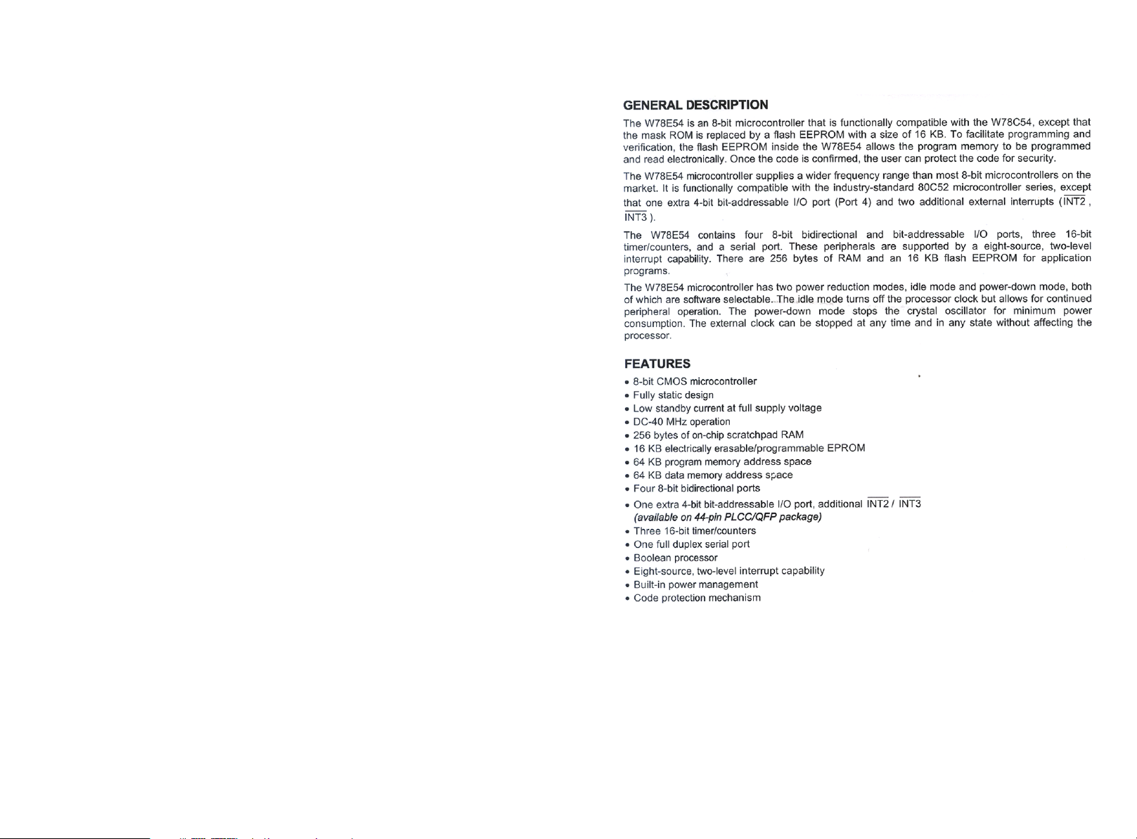
This unit's circuit can be divided into six parts.
1.1 Source Circuit
Supplies power to each circuit unit.
1.2 Input Circuit
Selects one of four lines of input analog signals and sends it to the rear circuit.
1.3 Volume and Tone Adjusting Circuits
Adjusts master volume and treble and bass tone of input signals.
1.4 Power Amplification and Protection Circuits
Amplifies input signals' power to drive speakers to produce sound; Protects circuits of speakers
and power amplifier automatically in abnormal conditions.
1.5 Microphone Circuit
Adjusts volume and tone of signals from the microphone and superimpose them on left and right
channels after echo processing.
1.6 Main Board Control and Display Circuits
Receives control commands and send control signals to achieve control function. Drives the VFD
screen to show the current working mode.
9 The Explanation For Key Components
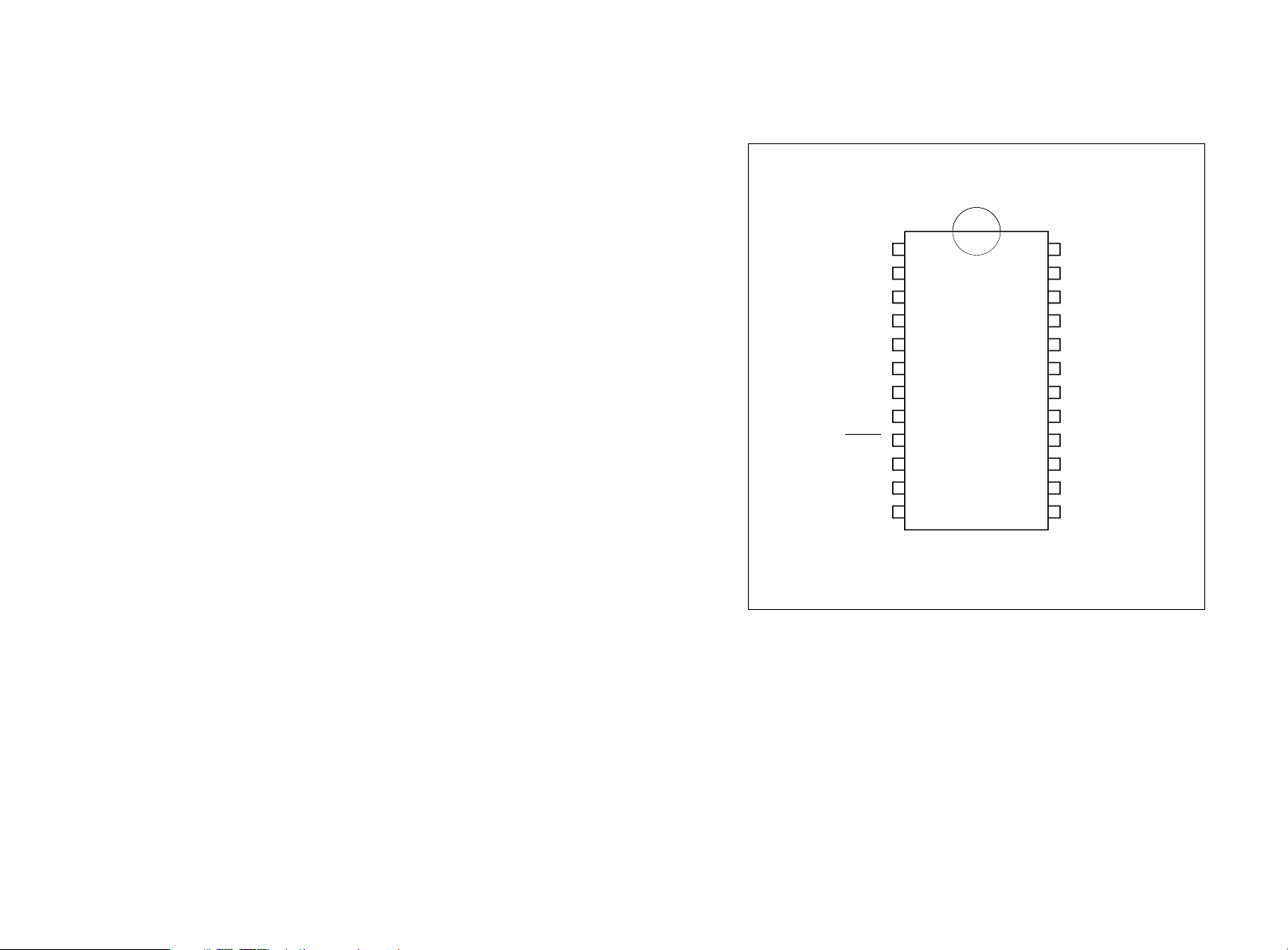
IC Sc6931P
VDD
1
XIN
2
XOUT
3
D1/REQ
D2/SCK
D3/DATA
D4/IDSW
EASY/U-COM
SLEEP
D-GND
A-GND LPF2 OUT
4
5
6
7
TEST
8
9
10
11
12 13
VCC
24
LPF1 IN
23
LPF1 OUT
22
OP1 OUT
21
OP1 IN
20
REF
19
CC1
18
CC2
17
OP2 IN
16
OP2 OUT
15
LPF2 IN
14
- 1 - - 26 -
Page 4
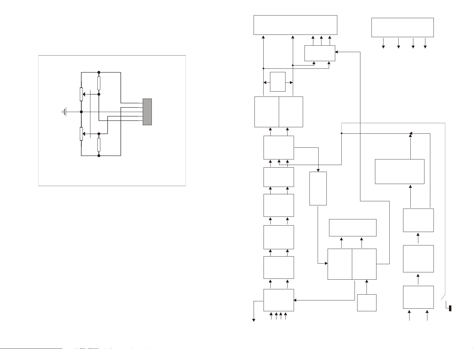
8.3.2 Schematic Diagram of The Potentiometer
Circuit
Speakers
Power
Supply
RPH01A
B50K
RPH01B
B50K
R917
2.2K
R918
2.2k
XP7
1
2
3
4
5
5PIN
L2
R2
GND
R3
L3
R
Power
Left Channel's
RP902
L
Circuit
Protection
Amplification
Power
Right Channel's
Echo
N903
Amplification
RPH01
Balance
Tone
N902
RP903
Adjustment
N901
Buffer
Amplification
C
SR
SL
and
2 CH
5 CH
Switch
BLOCK DIAGRAM (Figure 1)
Amplification
Echo
N905
SC6931
N906A
Amplification
Level Sampling
VFD
Screen
Echo
V601
Processing
Signal
Amplification
Tone
RP603
RP604
N906B
Adjustment
MIC Muffling
N601A
N601B
Level
Master
RP901
Volume
Adjustment
L
REC
R
Input
N401
CD4052
Selection
DVD
VCD
CD
TAPE
Spectrum
Front
Control
Panel's
Comparison
Function
Push
Matrix
Button
Two Lines
Amplification
Simultaneous
RP601
RP602
Volume
Adjustment
MIC1
MIC2
OK-SW
- 2 -- 25 -
Page 5
2. Volume adjustment, sound field processing and EQ adjustment
circuits.
All channel signals are sent to N402 inside which the independent volume adjustment,
EQ adjustment and all sound field modes process are performed.
The sound field processing and EQ adjusting circuit is mainly processing the L&R
channel signals. According to the schematic diagram, the L&R channel signals are
added simultaneously to the pins 15, 17, 13 and 16 of N402. When the unit mode is in
the Hi-Fi mode, the internal circuit of the pins 17&16 is connected and the other input
signals are cut off. At this time, only the L&R channel volume can be adjusted and only
the pins 31&32 send out signals. Therefore, the unit is in the 2CH output mode. The
unit mode is not in the Hi-Fi mode, other input signals are connected but the pins
17&16 signals are cutoff. At this time, all channel volumes can be adjusted
independently and the sound field processing or EQ adjusting of the L&R channels
can be performed. Finally, all channel signals pass out from the pins 31, 32, 33, 34,
35&36. The SW channel signal from the pin 36 reaches the amplified speakers to be
amplified through the SW output terminals. Other channel signals reach to the power
amplifying circuit to be amplified. The L&R channel signals will go through 1 grade
LPF and MIX amplification (Karaoke signals are overlapped into L& R channels).
st
3. Input signals detect, search and frequency spectrum sampling cir
cuits
3.1 Input signals detect and search circuit: The six channel signal lines of the input IC
N402 are connected with 100K sampling resistors R533, R534, R657, R676 and R678
respectively. The signals are mixed by these resistors and added to the opposite-phase
input terminal to be amplified. VD431 and C481 connected to N403B's output end
constitute half-wave rectifying filter circuit. Then the signals reach the voltage comparer
composed of N403A. The output end of N403A (SEARCH)is connected to the pin 28 of
CPU. This control signal is the search and detect signal: when it is low level, it enters the
search mode; when it is high level, it stops searching. Its works as follows:
3.1.1 When this unit is getting started, the A&B control signals from the pins 38&39 in
the domination of the CPU's inter program are added to the input select circuit to
search circularly once. When there are no signals in these four input connectors, the
VCD mode stops automatically. When there are signals in one of the four connectors,
AC signals will appear in all channels of the input N402. These AC signals are
amplified by N403B and rectified and filtered by VD434 and C481 to become DC
signals. At this time, the opposite-phase voltage of N403A is 0.01V. When this DC
voltage surpasses 0.01V, the output end of N403B sends out a high level (SEARCH)
close to positive power supply voltage (A+6V) which reaches the pin 28 of CPU. CPU
keeps searching in the connector in which there are input signals and the unit will play
normally.
1.2.2 When press the SEARCH on the front panel, CPU sends out A&B control
signals again to start searching. Meanwhile, the pin 27 (EX) sends out a high level
which makes V446 inductive. The emitter of V446 sends out a high level which passes
through R498 which makes the opposite-phase voltage of N403A to be 0.4V. That is
to say, if you want to stop searching of CPU, the gained voltage after the input signals
are rectified and filtered must exceed 0.4V. This voltage is higher than 0.01V when
this unit is getting started in order to avoid that the CPU receives signals mistakenly
and stops searching due to the large external interference signals. If the input signals'
amplitude is not high enough, CPU will continue searching. When the amplitude is
high enough, N403A sends out high level to the pin 28 to stop searching. The pin 27
(EX) will become low level again and the opposite-phase voltage of N403A will also
returns back to 0.01V. The whole searching process is finished.
- 3 - - 24 -
Page 6

R640
4.7k
L4
1
101
4558
-12V
N903A
C911
R921
27K
N902B
R908
10K
TREBLE
RP903A
B50K
R907
10K
10k
R905
8 4
3
2
+12V
R920
27k
R919
10k
R2L2L3R3GND
12345
XP7
T obanlance B o ard
7
4558
C907
101
5
6
R911
10K
C905
152
BASS
R909
22K
C906
683
B50K
RP902A
R910
10K
C903
1u/16V
7
N901B
4558
6
10k
R901
RP901A
10k
R906
5
R903
100K
B50K
123
XP4
3PIN
L1
R1
GND
To AMP Board
R924
101
C912
5PIN
+12V
84
R913
10K
RP903B
B50K
TREBLE
R912
10K
C901
-12V
C952
B50K
RP901B
R4
R926
100k
R925
100k
7
27k
4558
N903B
5
6
R923
27K
R922
10K
1
N902A
4558
-12V
C910
101
3
2
R916
10K
C908
152
BASS
R914
22K
683
C909
B50K
RP902B
R915
10K
C904
1u/16V
47u/16V
1
C902
N901A
4558
47u/16V
8 4
C913
+12V
3
2
C953
104
104
R904
100k
10K
R902
R4
12345
XP5
R4
2
N906A
101
R927
470k
-12V
C914
-12V
+12V
L4
6
6PIN
L4
-12V
+12V
GND
To AMP Board
+12V
VD602
1N4148
R643
10k
1k
R642
C636
4.7u/16V
R644
47k
C616
C614
4.7u/16V
C615
R619
15k
+5V
3
4558
8 4
+12V
1
4u7/16V
C603
101
LEVEL
C601
RP601
9014
V601
R641
C635
3.3k
R621
4.7u/16V
4.7u/16V
10k
R620
C630
47u/16V
R635
+12V
C605
47k
R603
-12V
C604
1k
R601
10u/16V
C50K
123
XP6
MIC1
R639
8.2k
R637
220k
R638
C633
4.7u/16V
470u/16V
R624
12K
562
C618
R622
10k
R623
15k
C619
104
561
C617
24
23
21
L1 IN
VCC
L1 OUT22O1 OUT
N905 SC6931
VDD1XIN2XOUT3D1/REQ4D2/SCK5D3/DATA6D4/IDSW7TEST8EASY/CM9SLEEP10DGND11AGND
30p
C628
2M
G601
30p
C629
C631
103
5.1V
VD601
150/0.5W
R618
47k
1
104
N601A
4558
C607
8 4
3
2
C606
47uF/16V
1k
R602
C602
10u/16V
C50K
RP602
4
4PIN
MIC2
GND
K-MUTE
Fr omMI Bo ard
C634
10u/16V
5.6k
100k
R625
10k
C620
20
O1 IN
104
+12V
47uF/16V
47u/16V
C621
REF19CC118CC2
B50k
RP605
4.7k
R946
10k
R636
C627
C623
4.7u/16V
C632
C625
R626
15k
224
C622
224
104
C624
17
16
15
O2 IN
O2 OUT
R634
10k
150mS
180mS
N906B
R610
8.2k
R609
20k
TREBLE
RP603
R608
12k
C610
R607
1.5k
R606
3.9k
10k
R604
C608
103
4.7u/16V
562
10k
15k
2.2k
R629
R628
R627
561
C626
14
13
L2 IN
L2 OUT
12
R630
10k
R631
10k
R632
10k
10k
R633
7
NJM4558
47p
R617
470k
C613
5
6
R616
10k
20k
R615
4.7k
8.2k
C612
104
R611
R612
BASS
B20k
RP604
B20k
471
C611
R614
10k
R613
123
C609
10k
7
N601B
47p
NJM4558
5
6
R605
100K
10u/16V
Page 7

Page 8

47
CD
CD11C 50V1U±20%4×7 1.5 C903,C904,C941
48
CD
CD11C 50V10U±20%5×7 2 C601,C602,C608
49
CD
CD11C 16V47U±20%5×7 2 C620,C630
50
CD
CD11 35V220U±20£¥10× 15
5
C956,C947
51 DIODE 1N4004 VD912,VD914
52 DIODE 1N4148 VD903~VD911,VD916,VD602
53
VOLTAGE
REGULATOR
DIODE
5.1V 1/2W VD601,VD915
54
VOLTAGE
REGULATOR
DIODE
24V 1/2W VD913
55 TRIODE 2N5551 V901
56 TRIODE 9014C V601
57
IC
LM324N DIP N907,N910,N911,N912
58
IC
NJM4558D DIP N901~N903,N906,N601
IC
4558C DIP N901~N903,N906,N601
59
IC
CD4013BCN DIP N908
60
IC
SC6931P DIP N905
61
CRYSTAL
OSCILLATOR
2.00MHz 49-U G601
62 VFD YW-3707A VFD901
63
LIGHT
TOUCH
RESTORE
SWITCH
VERTICAL 6×6×1 S901~S906
64
PCB
9217-4
65
CONNECTION
CORDS
¦µ
0.6 SHAPED 7.5mm
W1~W4,W7~W9,W11~W13,W16,W19~W22,W29,
W31~W34,W37,W38,W43,W46,W49,W52,W54,
W56~W58,W62,W65~W69,W74,W75,W81,W82,W83,
W90~W93,W99,W102,W103,W114,W116,W117
66
CONNECTION
CORDS
¦µ
0.6 SHAPED 10mm
W5,W17,W18,W23~W28,W35,W36,W39,W40,W42,
W47,W48,W59,W64,W70~W72,W76,W84~W86,W94,
W95,W98,W100,W101,W104,W109~W112,W115
67
CONNECTION
CORDS
¦µ
0.6 SHAPED 12.5mm
W10,W14,W15,W30,W44,W51,W61,W77,W78,W88,
W89,W107,W108,R1013
68
CONNECTION
CORDS
¦µ
0.6 SHAPED 15mm
W6,W41,W45,W50,W53,W55,W60,W63,W73,W79,
W80,W87,W96,W97,W113
69
CONNECTION
CORDS
¦µ
0.6 SHAPED 20mm
W105,W106
CORDS 24# 50mm BLACK
70 RAFT CORDS
3P360 2.5 2 PLUG WITH L
NEEDLE
XP3
71 RAFT CORDS
5P60 2.5 2 PLUG WITH L
NEEDLE
XP7
72 RAFT CORDS
3P80 2.5 2 PLUG WITH L
NEEDLE
XP2
73 RAFT CORDS
3P360 2.5 2 PLUG WITH L
NEEDLE , 2P SHIELDED
XP4
74 RAFT CORDS
4P60 2.5 2 PLUG WITH L
NEEDLE, 3P SHIELDED
XP6
75 RAFT CORDS
6P360 2.5 2 PLUG WITH L
NEEDLE, 2P SHIELDED
XP5
76
SOFT SPONGE
SPACER
10×10×5 DOUBLE
FACED, HARD
VFD/PCB
Page 9

Page 10

8.2 Front Panel's Control Board
NO. DESCRIPTION
SPECIFICATIONS / PART
NUMBER
LOCATION SPECIFICATIONS
1
CARBON FILM
RESISTOR
1/4W470¦¸±5% SHAPED
10
R979,R990,R994,R997,R1000,R1003,R1006,R1009,R1010
2
CARBON FILM
RESISTOR
1/4W1K±5% SHAPED 10
R601,R602,R961,R964,R967,R970,R982,R988,R1016,
R1012,R1007,R985,R1014,R642
3
CARBON FILM
RESISTOR
1/4W1.5K±5% SHAPED 10 R607
4
CARBON FILM
RESISTOR
1/4W2.2K±5% SHAPED 10 R629,R1004,R977,R978
5
CARBON FILM
RESISTOR
1/4W3.3K±5% SHAPED 10 R991,R621
6
CARBON FILM
RESISTOR
1/4W3.9K±5% SHAPED 10 R606
7
CARBON FILM
RESISTOR
1/4W4.7K±5% SHAPED 10 R1001,R611,R946,R640
8
CARBON FILM
RESISTOR
1/4W5.6K±5% SHAPED 10 R639
9
CARBON FILM
RESISTOR
1/4W10K±5% SHAPED 10
R901,R902,R905~R908,R910~R913,R915,R916,R919,
R922,R957,R971,R989,R995,R981,R987,R1015,R604,
R613,R614,R616,R620,R622,R625,R627,R630~R634,
R636,R643
10
CARBON FILM
RESISTOR
1/4W12K±5% SHAPED 10 R608,R624
11
CARBON FILM
RESISTOR
1/4W15K±5% SHAPED 10 R623,R626,R628,R619
12
CARBON FILM
RESISTOR
1/4W20K±5% SHAPED 10 R975,R976,R609,R615
13
CARBON FILM
RESISTOR
1/4W22K±5% SHAPED 10 R993,R996,R999,R1002,R984,R1008,R1005,R909,R914
14
CARBON FILM
RESISTOR
1/4W47K±5% SHAPED 10 R973,R974,R980,R983,R959,R960,R603,R618,R644
15
CARBON FILM
RESISTOR
1/4W100K±5% SHAPED10R903,R904,R925,R926,R962,R965,R968,R972,R963,
R966,R969,R992,R958,R605,R638
16
CARBON FILM
RESISTOR
1/4W220K±5% SHAPED
10
R1011,R637
17
CARBON FILM
RESISTOR
1/4W470K±5% SHAPED
10
R927,R617
18
CARBON FILM
RESISTOR
1/4W30K±5% SHAPED 10 R920,R921,R923,R924
19
CARBON FILM
RESISTOR
1/4W8.2K±5% SHAPED 10 R998,R610,R612,R641
20
CARBON FILM
RESISTOR
1/2W2K±5£¥ SHAPED 12.5
R986
21
CARBON FILM
RESISTOR
1/2W150¦¸±5% SHAPED
12.5
R635
22
ROTATING
POTENTIOMETER
A145GOED-H1B503-007 RP901
ROTATING
POTENTIOMETER
A145GOED-H1B503-00701
RP901
ROTATING
POTENTIOMETER
A145GOED-H1B503-00702
RP901
23
ROTATING
POTENTIOMETER
A145GOED-H1B503-008 RP902,RP903
8.2.1 Main Parts List of The Front Panel's Control Board
1. A+25V passes C941 and R983 and adds an instantaneous high level at the Pin 12 of
N907D when this unit gets started. According to the above characteristics, the Pin 14 sends
out a voltage which is comparatively closer to the voltage of the power supply B+23V. This
voltage measures about +17V and is fed back to the Pin 12 through R960. Then this voltage
is divided into about +8.5V by the resistor R959. That is to say, the inphase voltage of the
calculating amplifier N907D keeps at about +8.5V. At the same time, +8.5V is divided by
VD903, R971 and R972 and the voltage of the Pin13 of N907D measures about +7.5V. That
is to say, the inphase opposition of N907D keeps at about +7.5V. At this moment, the inphase
voltage (ca +8.5V) of the calculating amplifier N907D is higher than the inphase opposition
voltage (ca +7.5V). The output Pin 14 also keeps at about +17V. Therefore, the above status
retains. The Pin 14's high level of +17V passes R961 and reaches the display screen and
lightens the VCD indicator. The 0 level is obtained at the controllers A&B of the electronic
switch in the input circuit. According to the real value table, the electronic switch elects the
VCD input mode. C941 is the open restoration capacitor because of which the input mode
is switched to the default VCD. The inphase opposition voltage of another three calculating
amplifiers is +7.5V (Their inphase opposition ports are connected together), but the positive
voltage doesn't exist in the inphase ports. According to the voltage comparing characteristics,
there is not the high level output in the inphase opposition ports. The other three input modes
are shut off.
2. When we select other input modes, for instance, selecting DVD mode, we press the switch
S903. The voltage of B+23V passes R984, S903 and R965 and is divided into about +18V
voltage which is sent to the inphase port of N907A. At the same time, the +18V voltage is
divided by VD905, R971 and R972 and there is about +17V level input at the inphase
opposition port of N907A. The high level from N907A is fed back by R966. When loosening
S903, N907's working voltages (The working principle is the same as that in the abovementioned VCD mode.) are as follows: +8.5V at inphase port, +7.5V at inphase opposition
port, +17V at output port. As mentioned before, the inphase opposition port's voltage is +17V
when the switch is turned on. This voltage also reaches the calculating amplifier N907 in the
VCD mode. Because the inphase port of N907D remains +8.5V and the inphase opposition
port increases to +17V, the original output mode is breached and the high level cannot be
sent out. Therefore, the VCD mode is shut off. At this moment, the high level of +17V of
N907A's output is divided into two lines: One line is sent to the display screen by R967 to
lighten the DVD indicator. Another line is divided by VD908, R974 and R975 and sent to the
Port B of the electronic switch in the input circuit. Now, the Port A of N401 is 0 level and the
Port B of N401 is 1 level. According to the real value table, the electronic switch selects the
DVD mode, and the whole process is finished. When selecting other modes and pressing
other switches, the caused motions are the same as above ones.
- 8 -- 19 -
Page 11

6.2 Channel and MIC Delay Selection
The delay circuit is made up of the D triggers N908A, N908B and voltage comparers N910B,
N910C, N911A. The inching switch S905 is the channel selection button in the front panel.
S906 is the MIC delay selection button.
The Real Value Table of the D Trigger
Input Port
CLK
/
/
D
0
1
0
R
/
0
0
0
0
D, R and S are the controllers. It's low level when R is grounded. CLK is the triggering port
whose output mode overturns when a high level comes. When A+25V passes through R980
and R991, the inphase opposition voltage of those four voltage comparers is divided into
about +1.6V. The working modes are as follows. (Figure 8)
Figure 8
S
1
0
0
0
Output Port
Q
1
1
0
1
~
O
0
0
1
0
R990
VD916
V-5CH
XP3
1
2
3
A
B
Ex
8.1.2 Schematic Diagram Of The Main Power Amplifying Board
L
R
V427
C9014
V426
Y401
1 2
3 4
1N4148
VD418
VD405
1N4148
C9014
V421
C411
1u/16V
+33V
R433
V409
D718
V407
2N5551
2N5551
V430
220
R459
R409
150
V404
2N5401
R404
4k7
R403
4k7
V401
2N5551
C439
47u/35V
C9014
DC 24V
1N4004
VD407
5 6
10k
VD409
12V
R448
R447
1M
R446
47k
R461
2.7k
R435
3.9k
R414
220
22k
R413
V402
2N5551
C417
10u/50V
C416
C415
220u/25V
V425
10k
C9015
10k
R445
V424
C9014
R444
10k
47k
R462
1k
R443
V423
C9014
VD406
1N4148
104
R439
10/2W
C413
3.9k
R434
V410
B688
-33V
R416
R415
0.25/3W
0.25/3W
C433
R411
C404
680
R408
C402
R402
C401
2N5401
V408
10p
3k
V406
33
C403
R405
10k
271
22k
10u/16V
V431
2N5401
R412
1.2k
C9014
C405
47u/25V
V403
220
R401
R460
R410
150
V405
2N5551
33
22k
R407
VD402
1N4148
VD401
1N4148
2N5551
R406
1k
C440
47u/35V
R4
L4
C436
C435
DC 24V
Y402
220u/25V
220
R463
C
10u/50V
10u/50V
123456
C412
1u/16V
+33V
2N5551
V432
220
R425
150
C441
47u/35V
220
R417
SL
SR
~25V
C438
10u/50V
C437
10u/50V
V422
C9014
D718
V419
2N5551
V417
V414
2N5401
R420
4k7
R419
4k7
C406
VD408
1N4004
C418
100u/35V
V435
VD419
1N4004
V434
C9014
R442
10k
R441
10k
R440
10/2W
2.7k
R438
3.9k
R436
V412
V411
10u/16V
R437
R431
R432
0.25/3W
0.25/3W
R430
220
10p
C434
22k
R429
3k
R427
R428
1.2k
C409
33
V416
C9014
C410
680
2N5551
R424
C408
47u/25V
10k
R421
271
C407
2N5551
22k
R418
FL401
R450
47/3W
VD410
1N5404
C9014
220/3W
R451
R453
V428
2N5551
+12V
104
C414
3.9k
33
V413
-33V
B688
V420
V418
2N5401
V433
2N5401
R464
R426
150
V415
22k
R423
2N5551
VD404
1N4148
VD403
1N4148
2N5551
R422
1k
C442
47u/35V
From Tra ns
0
~25V
224
C420
C419
224
FL402
T6.3A/250V~
VD411
1N5404
C421
6800u/35V
+33V
C423
470u/25V
3k3
VD415
12V
C425
47u/16V
C427
100u/16V
220
+12V
6.8V
VD417
R4671kR4681kR4691kR4701kR4711kR4721kR4731kR474
VCD R
T6.3A/250V~
VD413
1N5404
VD412
1N5404
C422
6800u/35V
R452
220/3W
C424
-33V
470u/25V
R454
3k3
VD414
12V
V429
2N5401
C426
47u/16V
C428
100u/16V
-12V
XS4
102
C432
C431
1k
R4571kR458
1k
R455
C429
47u/16V
VCD L
3
X13Y
168
N401
CD4052
X012X114X215X311Y01Y15Y22Y3
4
CD L
CD R
DVD R
102
R 1
6A10B9
INH
DVD L
12345
6
XS5
6PIN
R4
L4
-12V
+12V
To VFD Board
123
L 1
To VFD Board
123
XS3
3PIN
VEE
7
VD416
TAPER
3PIN
A
B
Ex
R466
47K
R465
47K
C444
10u/16V
C443
10u/16V
1k
R456
-12V
6.8V
C430
47u/16V
1k
TAP EL
REC L
REC R
- 9 - - 18 -
Page 12

6.2.1 Channel selection section.
30 CD CD11 25V220U±20%8×12 3.5 C415,C416
31 CD CD11 35V470U±20%10×20 5 C423,C424
32 CD CD11 50V1U±20%5×11 2 C411,C412
33 CD CD11 50V10U±20%5×11 2 C435,C436,C437,C438,C417
34 CD CD11 35V47U±20%6×12 2.5 C439,C440,C441,C442
35 CD CD11 35V100U±20%8×12 3.5 C418
36 CD
LUA 35V6800U±20£¥30×45 10
C421,C422
37 DIODE 1N4004 VD407,VD408,VD419
38 DIODE 1N4148 VD401~VD406,VD418
39 DIODE 1N5404 VD410~VD413
40
VOLTAGE
REGULATOR
DIODE
12V 1/2W VD415,VD414,VD409
41
VOLTAGE
REGULATOR
DIODE
6.8V 1/2W VD417,VD416
42 TRIODE 2N5401 V404,V408,V414,V418,V429,V431,V433
43 TRIODE 2N5551
V401,V402,V403,V405,V407,V411~V413,V415,V417,
V428,V430,V432
44 TRIODE 9014C
V406,V416,V421,V422,V423,V424,V426,V427,V434,V4
35
45 TRIODE 9015C V425
46 TRIODE KB688O V410,V420
TRIODE KB688Y V410,V420
47 TRIODE KD718O V409,V419
TRIODE KD718Y V409,V419
48 IC CD4052BCN DIP N401
49 RELAY JH4237-024-2H DC24V Y401,Y402
50 PCB
4217£-3
51
TERMINAL
SOCKET
AV6-8.4-3B XC2
52
TERMINAL
SOCKET
AV4-8.4-3B XC1
53 SOCKET 3 PIN 2.5mm XS3,XS4
54 SOCKET 6 PIN 2.5mm XS5
55
SOCKET FOR
EXTERNAL
CORDS
WP6-1B XL1
56 POLE SOCKET WP4-10A XC3
57
CONNECTION
CORDS
¦µ
0.6 SHAPED 7.5mm
W29,W32,W35,W36,W39,W48,W54,W58,W13
58
CONNECTION
CORDS
¦µ
0.6 SHAPED 10mm
W10~W12,W15,W19~W21,W27,W31,W33,W34,
W37,W43,W44,W47,W51,W53,W55
59
CONNECTION
CORDS
¦µ
0.6 SHAPED 12.5mm
W14,W16,W49,W50,W56
60
CONNECTION
CORDS
¦µ
0.6 SHAPED 15mm
W5,W7,W17,W18,W22,W23~W26,W28,W30,W45,W46
,
W40,W41,W52
61
CONNECTION
CORDS
¦µ
0.6 SHAPED 20mm
W38,W42,W57
62 FUSE TUBE T6.3AL 250V FL401,FL402
63
LARGE
RADIATOR
204×80×61 AB217 CONNECT TO THE MAIN AMP BOARD
64 FUSE HOLDER 0 FL401,FL402
65 SMALL CHIP AB207 FIX THE TRIODES V406 AND V416
66 TAPPING SCREW PB 3×12H COLOR ZINC 2 FOR SMALL CHIP AND LARGE RADIATOR
67 TAPPING SCREW PWT 3×8×8 COLOR ZINC 2 FOR PCB/RADIATOR
68
MACHINE
SCREW
PWM 3×16×8 COLOR ZINC 4 FOR POWER TUBE / LARGE RADIATOR
69 SCREW NUT M3 POWER TUBE SCREW
70 SCREW SPACER
¦µ
3×7.2×0.5
POWER TUBE SCREW
71 SPRING SPACER
¦µ
3
POWER TUBE SCREW
72 MICA SPACER 24×20×0.1 4 FOR POWER TUBE / LARGE RADIATOR
When this unit gets started, +5V is charged by C943 and adds an instantaneous high level
at the Port S. The Port R is grounded and is low level. According to the real value table, the
Port Q sends out high level and the Port Q' sends out low level. Although the Port S becomes
low level because C943 is full of charges, the Port D still keeps the original output modes for
it stays in low level caused by the connection between the Ports Q and Q'. The high level of
the Port Q of N908A is about 5V and reaches the inphase port of N910 through R1015.
However, the inphase opposition of N910A is about 1.6V. Thereby, the output port of N910A
sends out high level according to the voltage comparison characteristics. The level is sent
by R1016 to the display screen to lighten 2CH indicator. This unit switches to the 2CH mode
automatically when it gets started.
When pressing the switch S905, a triggered high level is sent to CLK. The output mode is
revered. Port Q becomes low level and Port Q' becomes high level. Because Port Q' is
connected to Port D, Port D also remains high level. Let go the switch S905, the input mode
remains due to the reaction of Port D. Because Port Q is low level, the positive voltage of the
inphase opposition of N910A will disappear. According to the voltage comparison characteristics, there's no high level sent out from the output port of N910A and thus the 2CH mode is
shut off. Meanwhile, the high level passes through R989 and reaches the inphase port of
N911A. The high level from the output of N911A is divided by R990 into two lines: One line
reaches the display screen to lighten the 5CH indicator. Another line reaches to the amplification circuit via VD916 to switch on the multi-channel output relay Y402. The channels C,
SR, SL are opened and there will be 5CH outputs. When pressing the switch S905, the output
mode is reversed once and returns to the 2CH mode.
6.2.2 The MIC delay selection section.
Its working principle is approximately the same to the channel selection. The difference is
that output Q and Q' will be divided into two lines: One line is sent to the voltage comparer.
Another line is sent to the Pins 4&6 of the echo processing IC N905 to control the delay time
of MIC signals in the echo circuit.
- 10 -- 17 -
Page 13

6.3 The spectrum analysis section (Figure 9)
NO. DESCRIPTION
SPECIFICATIONS / PART
NUMBER
LOCATION SPECIFICATIONS
1
CARBON FILM
RESISTOR
1/4W680¦¸±5% SHAPED 10
R408,R424
2
CARBON FILM
RESISTOR
1/4W1K±5% SHAPED 10 R467-R474,R455,R456,R457,R458,R443,R406,R422
3
CARBON FILM
RESISTOR
1/4W3K±5% SHAPED 10 R411,R427
4
CARBON FILM
RESISTOR
1/4W3.3K±5% SHAPED 10 R453,R454
5
CARBON FILM
RESISTOR
1/4W3.9K±5% SHAPED 10 R433,R434,R436,R437
6
CARBON FILM
RESISTOR
1/4W4.7K±5% SHAPED 10 R403,R404,R419,R420
7
CARBON FILM
RESISTOR
1/4W10K±5% SHAPED 10 R405,R421,R445,R448,R444,R446,R441,R442
8
CARBON FILM
RESISTOR
1/4W22K±5% SHAPED 10 R402,R407,R413,R418,R423,R429
9
CARBON FILM
RESISTOR
1/4W47K±5% SHAPED 10 R462,R465,R466,R461
10
CARBON FILM
RESISTOR
1/4W1M¦¸±5% SHAPED 10
R447
11
CARBON FILM
RESISTOR
1/4W1.2K±5% SHAPED 10 R412,R428
12
CARBON FILM
RESISTOR
1/4W220¦¸±5% SHAPED 10
R401,R417
13
CARBON FILM
RESISTOR
1/4W150¦¸±5% SHAPED 10
R409,R410,R425,R426
14
CARBON FILM
RESISTOR
1/4W2.7K±5% SHAPED 10 R435,R438
15
CARBON FILM
RESISTOR
3W220¦¸±5% R-SHAPED 20×8
R451,R452
16
CARBON FILM
RESISTOR
1/2W220¦¸±5% SHAPED 12.5
R459,R460,R463,R464,R414,R430
17
CARBON FILM
RESISTOR
2W10¦¸±5£¥ R-SHAPED 20×8
R439,R440
18
CARBON FILM
RESISTOR
3W47¦¸±5£¥ R-SHAPED 20×8
R450
19
CEMENT
RESISTOR
3W0.25¦¸±5£¥ R-SHAPED 25×8
R415,R416,R431,R432
20
PORCELAIN
CAPACITOR
50V 10P ±10% NPO 2.5mm C433,C434
21
PORCELAIN
CAPACITOR
50V 33P ±10% NPO 5mm C404,C405,C409,C410
22
PORCELAIN
CAPACITOR
50V 271 ±5% NPO 5mm C402,C407
23
PORCELAIN
CAPACITOR
50V 102 ±10% 5mm C431,C432
24
TERYLENE
CAPACITOR
100V 104 ±10% 7mm C413,C414
25
TERYLENE
CAPACITOR
100V 224 ±10% 8mm C419,C420
26 CD CD11 16V10U±20%5×11 2 C401,C406,C443,C444
CD CD11 25V10U±20%5×11 2 C401,C406,C443,C444
27 CD CD11 16V47U±20%5×11 2 C425,C426,C429,C430
28 CD CD11 16V100U±20%6×12 2.5 C427,C428
29 CD CD11 25V47U±20%5×11 2 C403,C408
We have mentioned a LEVEL signal in Chapter 4 Volume, Tone and Balance Adjusting
Circuits. That signal is the spectrum analysis source. It was sent to 6-band spectrum level
display circuit composed of 6 voltage comparers: N911D, N911C, N911B, N912D, N912C
and N912B.
8 Detailed Circuit Explanations
8.1 The Power Amplifying Board
8.1.1 Main Parts List of The Matin Power Amplifying Board
The stronger the source
signal is and the more
the luminescent bands
there are, the higher the
indicated level.
LEVEL
The detailed working process: The inphase opposition voltages of these six voltage
comparers have their corresponding voltages respectively for the distributing resisters
are connected differently. We call these separate voltages valve voltages: N912Bca 0.2V,
N912Cca 0.4V, N912Dca 0.8V, N911Bca 1.6V, N911Cca 3.5V, N911Dca 5.2V. It's obvious
that their valve voltages increase by degrees. The LEVEL signal is coupled by R1010,
commutated and filtered by VD911 and C946. The output DC voltage is added at the inphase
port of these six voltage comparers. According to the voltage comparison characteristics,
when the source signal's voltage surpasses the valve voltage, the corresponding voltage
comparer's outputs will export high level to lighten the display screen's illuminant. For
instance, when input signal's voltage is 0.3V which exceeds the inphase opposition port's
0.2V valve voltage of the bottom N912B. Then the output of N912B exports high level to
lighten the bottommost illuminant on the display screen. On the other hand, 0.3V voltage
does not exceed the valve voltage of another five voltage comparers, so they will not export
high level. Neither the display screen can be lightened. When the input signal exceeds 5.3V
which is beyond the valve voltage of these six voltage comparers. Therefore, these six
voltage comparers' output ports will sent out high level and all six-band illuminants on the
display screen are lightened to achieve maximum display. Because the music signals are
changing continuously, these six illuminants will rise or fall accompanying with strong or
weak music signals. This is the basic working principle of the spectrum display circuit.
N911D
N911C
N911B
N912D
N912C
N912B
(Figure 9)
PL6
PL5
PL4
PL3
PL2
PL1
- 11 -
Illuminant
- 16 -
Page 14

7.2.3 Short Circuit over-current Protection
7 Power Amplification and Protection Circuits
The channel R's output end is parallel connected with a over-current sampling triode V421.
R415 and R416 are over-current sampling resistor. When current soars up sharply due to
short circuit, the potential difference between R415 and R 416 also increases. The current
passes to the base and emitter of V421 through R433 and R434. When their potential difference is beyond 0.7V, V421 is conducted and its collector's potential decreases. Finally, the
current passes VD405 and R443 to make V425 conducted and thus the relay is shut off.
Over
Current
Potential Difference
Between R415 and R416
Increases
V421
Conducted
V425
Conducted
Relay
Shut Off
7.3 Multi-channel Control Circuit
In the front panel circuit introductions, we have explained that when we choose the multichannel output mode, N911A's output end sends out high level which reaches the base of
a compound tube composed of V434 and V435 through R441. V434 and V435 are
conducted and there is current in the coil Y402. Y402 is switched on. Channels C, SR and
SL pick up signals from channels R and L and then send them out.
The power amplification circuit is this unit's hard core which is working under high voltage
and large current volume, so its failure rate is very high. A protection circuit is added to the
power amplification's output to protect the amplifier and speakers' circuits. In addition, a
multi-channel switching circuit is also connected to the output of AB217. We take the R
channel as an ample to analyze the circuit as shown in the figure 10.
R
INPUT
AC Negative
Feedback R413,
R408,C403
Difference
Amplification
V401,V402
Mirror Image Constant
Current Source
V403,V405
VD401,VD402
Voltage
Amplification
V404
Compound Power
Amplification(NPN)
V430,V407,V409
Temperature
Compensation
V406
Compound Power
Amplification(PNP)
V431,V410,V408
Speakers
Protection
Circuit
- 15 -
Figure 10
- 12 -
Page 15

7.1 Power amplification section
Over +4V V424 Conducted
Outp ut End
V425
Conducted
Relay Shut
Off
Below -4V V423 Conducted
7.2.1 Delay switch-on protection circuit
The R channel signals are coupled by R401 and C401 and sent to the base of difference
amplification section V401. V401 and V402 comprise the difference amplification circuit
of single input and output. The sound signal is sent from the collector of V401 to the base
of the voltage amplification section V404. The amplified signals reach the compound power
amplification section. V403, V405, VD401 and VD402 constitute the mirror image constant
circuit. VD401 and VD402 provide a constant base current to V403 and V405. The emitter
resistor of V403 determines the working current of the difference amplification section and
the V405's emitter resistor determines the working current of the voltage amplification section.
V430, V407 and V409 constitute the upper tube (NPN) of the compound power amplification
section. V430 and V407 are first parallel-connected to function as a triode (To raise the power)
and then compound V409 to constitute a NPN type compound tube (To make amplification
multiplied). V431, V408 and V410 constitute the bottom tube (PNP) of the compound power
amplification. Its circuit construction is the same as that of the upper tube except that it's PNP
typed after compounding. The temperature compensation section V406 has the following two
functions in the circuit: First, it is composed of the voltage reversed triodes of the same
parameters, so its working mode determines the static working current of the compound power
amplification section. That is to say, we can set up the static working point of compound power
amplification section through adjusting the V406 conducting level. The usual way is to change
the base resistor of V406. Second, it functions as automatically adjust the working mode of the
compound power amplification section when temperature rises. The adjusting process goes
as follows:
TOTAL OUTPUT CURRENT = WORKING CURRENT + LEAK CURRENT
When temperature rises, the leak current increases thus the total current increases (unfavorable condition). At the same time, the base current of V406 increases and Uce
decreases thus the output section's bias current decreases. Therefore, the working status
changes and the back working current decreases. The total current is limited in a certain range.
When this unit is getting started, +26V passes through R447 to charge C417. The positive
end voltage of C417 increases slowly. When the voltage supersedes 12V, VD409 (12V
voltage regulator diode) is penetrated and its negative end outputs high level which makes
the compound tube composed of V426 and V427 conductive. Therefore, their collectors'
potential is dragged down and there is current in the relay Y401. The relay is switched on.
The delay time depends on the constant of R447 and C417 charging time. The positive end
voltage of C417 is a key point through detecting which whether there is the voltage over +12V
to judge whether the whole protection circuit is started. When there is a voltage over +12V
and the relay is not switched on, it indicates that the problem only exists in the back components VD409, V426, V427 and Y401. When there is a voltage below +12 and the relay is
switched on, it indicates that the protection circuit is started and you need only to check the
corresponding circuits.
+26V
R447
charges
C417
Penetrates
VD409
V426 & V427
conducted
Y401
switched
on
7.2.2 Midpoint Over-voltage Circuit
A midpoint over-voltage sampling resistor R462 is connected to the output end of Channel
R (Channel L is R461). Because the power amplifying circuit is provided by twin power
supplies, the output end usually has two conditions: positive or negative voltage. They will
be analyzed respectively as follows. This protection circuit's protecting range is the voltage
above +4V or below 4V.
When the output end voltage surpasses +4V, the base receives a voltage above +0.7V
due to the voltage division by R462 and R445. V424 is conducted and the collector's
potential is dragged down.
7.2 Protection Circuit
The protection of the power amplifier's output section is performed by a relay series connected between the output end and the speaker. The power amplifying circuit is not stable when
getting started and an impact current output will occur. If the output end has already been
connected to the speaker when getting started, BOO sound will come out of the speaker.
This is very harmful to the speaker. Therefore, we serial connect a relay between the output
end and speaker. In this way, when this unit is getting started, the relay is switched off and
the output end and the speaker will not be connected and thus the impact current will not
occur. The relay will open only when the circuit works stably. Therefore, the protection is
realized. In a similar way, when the circuit goes wrong and a high voltage and large current
will occur in the output end, the protection circuit will also cut off the relay to realize the
protection function. AB217 boasts its three protection functions: delay switch-on protection
circuit, midpoint over-voltage protection circuit and short circuit over-current protection
circuit. The working power of the protection circuit comes from a half-wave commutating
circuit composed of VD408 and C418. It's about +26V.
- 13 -
When the output end voltage is below 4V, the base of V423 receives a voltage below 0.7V
due to the voltage division by R462 and R445. V423 is conducted and the collector's
potential is dragged down..
According to the above statements, the collector's voltage will be dragged down whether
the output end potential is over +4V or below 4V. This low potential passes R444 and
makes the base's voltage of V425 decrease. V425 is conducted and thus its emitter's
voltage decreases. That is to say, the positive end voltage of C417 decreases and the
relay is shut off, thus the protection function starts.
- 14 -
 Loading...