

Page 1

Principle, Knowledge and Maintenance of
AV215T (RU)
Contents
Chapter One Product Description
Chapter Two Operating Principle
Section One Overall Structure
Section Two Volume Board
Section Three Signal Processing Board
Section Four CPU Board
Section Five Control Panel
Section Six Power Panel
Section Seven Power Amplifier Board and Protection Circuit
Chapter Three Maintenance Process
Page 2

Chapter One Product Description
AV215T (RU) is an advanced power amplifier with complete functions that adds
LCD to its predecessor as well as 16 kinds of spectrum displays in the sky-blue
background which makes it more extraordinary. The radio reception makes this type
of device the best choice for users who are fond of radios. Its main features are as
follows:
1. Built-in 5-track power amplifier that can adapt to AC-3/DTS and stereo music
playback. It is powerful with 80W main channel and 15W centre surround sound.
2. Mixing input interface of AC-3/DTS, VCD and DVD and DBB and stereo output
interface.
3. 6-channel volume control and independent level control as well as 7-band EQ.
4. Bass Enhancer system, cyber logic and Hi-Fi playback.
5. One button for movie, music and karaoke.
6. Multiple EQ modes that adapt to different music styles.
7. Automatic spectrum analysis and compensation, automatic signal compensation.
8. Multiple spectrum display modes.
9. Complete karaoke function including microphone independent volume control,
overall volume control, pitch adjustment, voice compensation, delay and echo
adjustment as well as the newly added earphone output.
10. Karaoke wide sound field function.
11. T uning function.
12. Intelligent protection of over-current and over-voltage.
Chapter Two Operating Principle
Section One Overall Structure
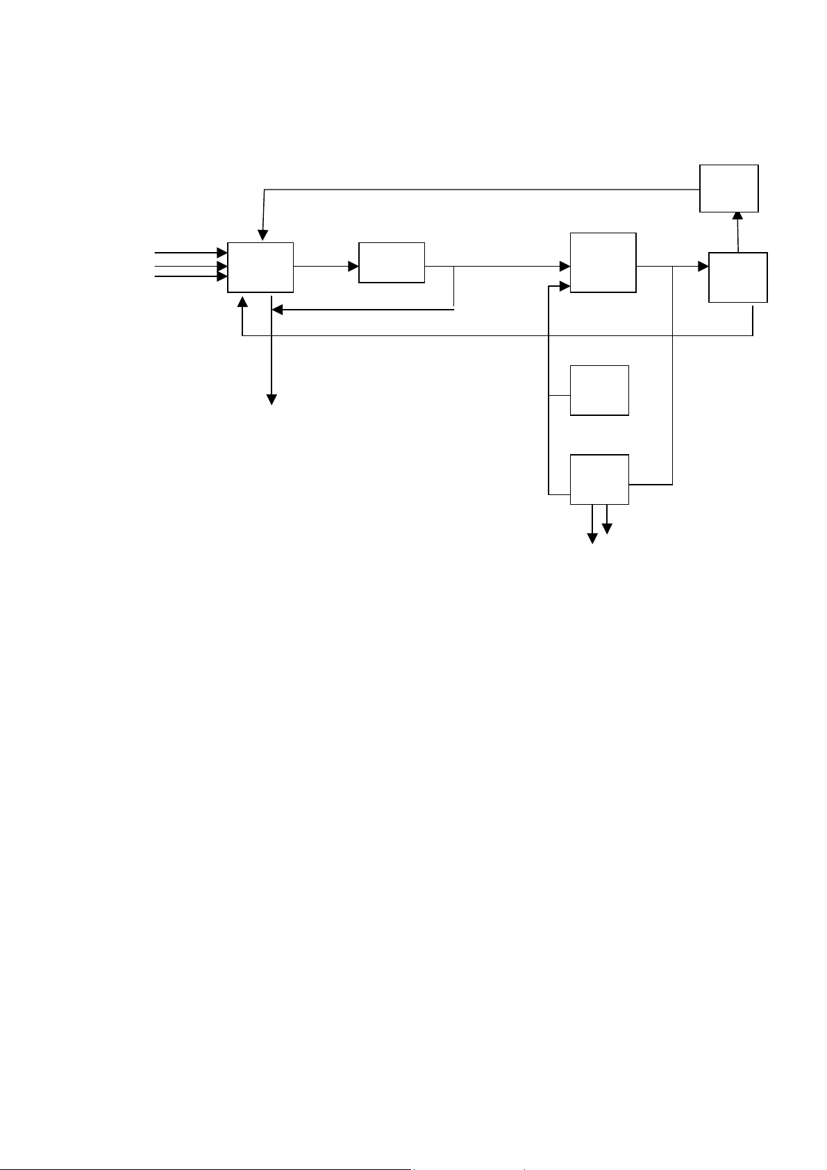
AV215T (RU) mainly consists of the following seven parts:
I. Volume Board: Select input signal source, cyber logic and bass enhancer.
II. Signal Processing Board: Karaoke signal processing and 5.1CH signal
amplification.
III. CPU Board: Overall control, frequency point gating, automatic circuit search.
IV. Control Panel: LCD display, remote control keyboard and backlight display.
V. Power Panel and Protection Circuit: Provide operating voltage required by unit
circuits and overall protection.
VI. Power Amplifier Board: Power amplification of 5.1CH signal or analog signal.
VII.
AV215T (RU) has four input modes: Radio input, VCD, DVD and 5.1CH.
The cyber logic function of AV215T (RU) is to get C/SR/SL/SW track signals by sampling
from L/R track and then processing through low-pass filter and adder subtractor. Mode
Tuner: Receive radio signal and send to amplifier for signal-processing.
Section Two Volume Board
Page 3
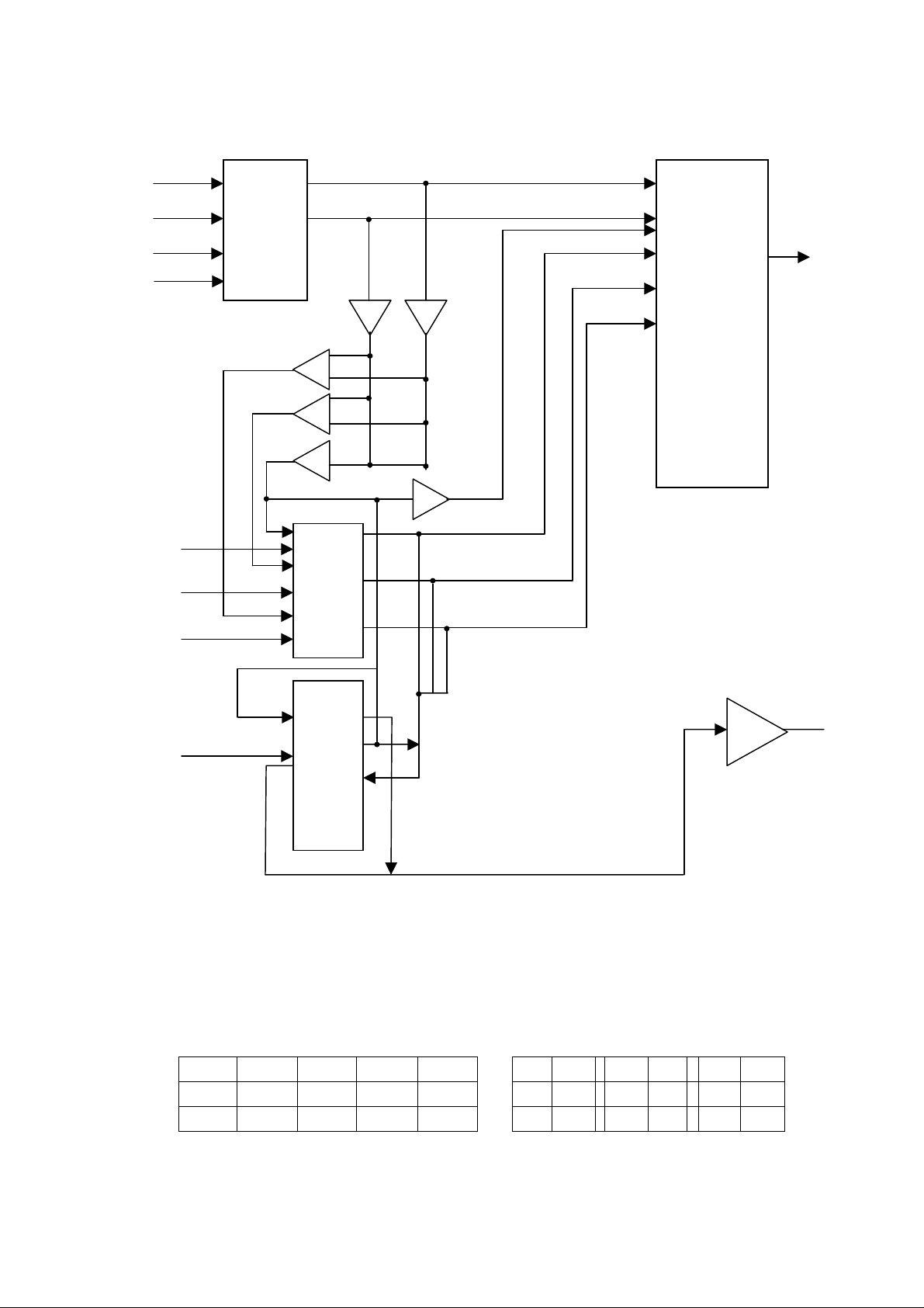
switch is achieved by using electronic analog switch. The signal flow chart is as follows:
N
N
N
N
N
N
N
N
Tuner
VCD
DVD
5.1CH
C
SR
SL
CD405
2
Electronic
switch
N101
S-C
S-SR
S-SL
107B
105B
105A
L
R
104A
CD
4053
Electro
nic
switch
OUT
N106
M62446
104B
107A
SWIN
CD
S-C
4053
SW
Electro
nic
switch
103
Input selection and sound field processing mode
The input selection of AV215T (RU) is achieved via electronic switches CD4052
and CD4053, the truth tables of which are as follows:
CD4052 Truth Table CD4053 Truth Table
Tuner VCD DVD 5.1 A X B Y C Z
A 0 0 1 1 0 X0 0 Y0 0 Z0
B 0 1 0 1 1 X1 1 Y1 1 Z1
108B
DISPLY
I.
5.1CH input mode: Now A/B/5.1CH control pins of M62446 are of high level. L/R
Page 4

track signal of 5.1 input is outputted from pin 3/13 of N101 and sent to IC N106 for
volume and tone adjustment; meanwhile, C/SR/SL signal on 5.1 input terminal is
respectively sent from pin 14/15/4 output of N410 to IC N106 for independent
volume adjustment. And SW signal is outputted via pin 4 of N103 and then send to
M62446 after being amplified by N107A.
Three analog input modes: AV215T (RU) totally has three analog input modes:
Tuner receiving signal/VCD/DVD, which are controlled via A/B signal respectively
(see details in truth tables).
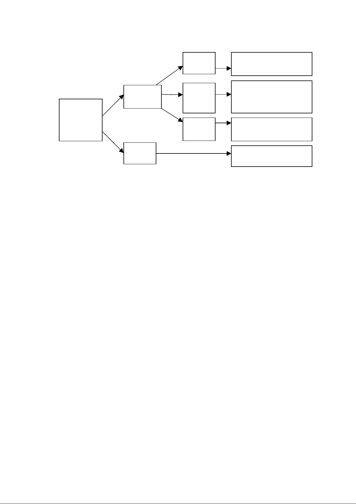
AV215T (RU) totally has three sound field modes: standard sound field, cyber logic
and Hi-Fi.
1. Standard sound field: Under overall CPU control, when bass enhancer is off, L/R
channel and subwoofer output are available; when bass enhancer is on, only L/R
channel output is available.
2. Hi-fi: Under overall CPU control, only L/R tracks output is available to M62446;
3. Cyber logic:
Pin 9/10 of electronic switch N101 (CD4052) select a series of analog L/R track
input signals according to the truth table. L/R signals are outputted from pin 13/3
via the internal electronic switch of N101, and divided into two ways. One way is
respectively sent into pin 13/15 of M62446, for electronic volume and tone control.
The other way produces SW/S-SR/S-SL/S-C signals via buffer, adder-subtractor
and low-pass filter. SW/S-SR/S-SL signals are sent to pin 12/2/5 of N102. N102
select cyber logic signal input (see truth table of CD4053) from cyber logic and
5.1CH signals, outputs C/SR/SL signals and sends into pin 11/8/9 of M62446 for
volume control. Still another way of SW signal directly sends to pin 6 of M62446
after being outputted from N107A. 5.1CH signal sent into M62446 is outputted
from pin 31-36 after volume and tone control, and then outputted to signal board
by XS20 power distributor.
The relation between sound sources in input circuit and sound processing modes is as
illustrated below.
II. Control circuit
Pin 23/26/27 of CPU (N100) output data, PVST and clock signal and send to pin
39/40/41 of M62446 to control pin 1/2/3/4 of M62446 to output control level, so as to
select input signal and spectrum sampling signal. It is worth noting that PVST signal
is a latch control signal. When data and clock of CPU are sent to M62446, an
identification signal will be added, indicating that this signal can only be used by
M62446 while other IC of I2C bus cannot use current data and clock signal.
Page 5
b
t
eld
d
t
d
d
Hi-fi
mode
Press INPUT
utton to
circularly
select
Two analog
input modes
Standard
sound
fi
Cyber
logic
5.1 inpu
mode
III. Frequency spectrum sampling circuit
Only S-C/S-SR/S-SL/SW signals are sampled during frequency spectrum sampling in
AV215T(RU)and added to pin 14 via a 150K sampling resistance. Another S-C cyber logic
signal is added to pin 1 of N103, called S-C. 5.1CH and LR-T of M62446 select sampling
signals. When cyber logic is selected, the control signal of 5.1CH is of low level while pin
9/11 of N103 is of low level. According to the truth table, it is known that the outputs are
X0/Z0. Sampling signal is grounded while LR-T is of H level. Select Y1, S-C'signal is
outputted from pin 15 of N103 to N108B, adding to OK-R signal for the amplification of
frequency spectrum signal, and then sent to frequency point gating and auto search circuits.
. Ⅳ Tuning function
This device has the tuning function which provides users a good functional option. It
directly controls radio-head and receives audio frequency signal mainly via CPU and then
outputs after amplified via power amplifier. The clock and data line of radio-head are
shared with LM62446 and the other two control lines are connected to CPU directly. L, R
signal processed by radio-head can be sent to N101 IC CD4052 directly to input the
selected track.
L/R channel output only. Soun
filed and EQ setup not available.
L/R/SW output only. Concer
hall sound filed and EQ setup
available
6CH output. Theater sound file
and EQ setup available
6CH output. Theater sound file
and EQ setup available
Section Three Signal Processing Board
The signal processing board superposes, mixes and amplifies 5.1CH signal sent from the
volume board, voice signals from the voice board and karaoke signal.
I. AV215T(RU)Karaoke Circuit
1. Function: this circuit processes human voice through power amplifier and
reproduces it via speaker. It includes human voice beautification circuit, wide sound field
processing circuit, karaoke echo and delay adjusting circuit.
Page 6
IC and its functions for karaoke
IC serial
number
N201 4558 Transmittal. Preamplification for karaoke signal
N200 PT2315 Volume control of karaoke, including tone control
N205 CD4053 Electronic switch
N209 PT2399 Karaoke echo processing
N207 CD4051 Karaoke delay adjustment
N208 CD4051 Karaoke echo control
N204 4558 Phase inverter
PT2315 functional pin
S/N Name of pin Description Remarks
1 REF Reference voltage (1/2VDD)
2 VDD Power supply
3 AGND Analog
4 TREB L
5 TREB R
6 RIN R channel input
7 LOUD-R R channel loudness control pin
9 LOUD-L L channel loudness control pin
11 LIN L channel input
12 BIN L
13 BOUT L
14 BIN R
15 BOUT R
16 RFOUT R channel output
17 LFOUT L channel output
18 DGND Digital
19 DATA (DATA)control data of sequence
20 LCK Clock input of sequence
8,10 NC Not connected
3. Flow chart of karaoke signal
Name of IC Functions
L/R channel treble control pins
L channel bass control input/output
R channel bass control input/output
transmission (DATA)
transmission
pin
pin
Page 7
MIC
N
N
N
N
N
N
N
N
N
N
201
200
B
202
203B
209
N205
204
202
207
100
V200
CP
208
Karaoke
mixed output
When the microphone is inserted, MIC signal is sent via MIC to the transmittal circuit
combined by N201A for amplification. Amplified MIC signal gives CPU a MIC
identification signal after N202A amplification, followed by VD201 rectification and
filtering control triode V200. CPU sends PKM signal, which is of low level, causing cutoff
of triode V103/V105 and enabling output of MIC signal; another way reaches pin 6/11 of
PT2315 after C219/C222 coupling, outputs from pin 16/17 after internal volume and tone
control, mixed into one way and sent to N202B and then reversely send to N203B for
amplification. Signals amplified by N203B are divided into two ways. One way is directly
outputted. The other way is outputted from pin 14 after being coupled by R222/C247 to
PT2399 for internal delayed reverberation adjustment, reversed by N204 and outputted by
mixing with karaoke signal. While OK-R is outputted from pin 14 after being gated by
N205 and superposed to L/R track.
In this circuit, the bass boost network made up of triode V201 connected to the
negative terminal of N202B is primarily for bass boost of 75HZ low frequency signal.
During delay adjustment for PT2399, first control signal is given to CPU, which
controls N207 after being expanded via N211 IC CD4049 and connects with pin 6 of
PT2399 by selecting different resistance values for purpose of delay adjustment.
Reverberation control is to change the resistance value at the connection point to R229,
so as to change the superposition on through connect signal for reverberation control.
The broadband processing control signal of SOK’s karaoke is in broadband mode
when it is of high level, when the signal of OK-R is the OK signal inverted by N204A.
A sense signal of OK-SW on the MIC plug conducts MIC signal detection together
with the network made up of V200. When MIC is not plugged, it is of low signal; when
plugged, it is of high signal.
Karaoke auto mute is also available. When P-KT fails to detect signal for a continuous
time, CPU will send a P-KM signal to mute karaoke and avoid MIC receiving noise, which
may affect on sound effect.
Signal flow chart of profiles
Pass
Page 8
AV215T (RU) has a special function that switching between 5 profiles is available
N
N
N
N
N
N
N
without karaoke. Its flow chart is as follows:
204
205
203
209
204
B
Mixed output
207
208
CD4094
When pin 9/10 are of high level, sampled L/R/C signals are outputted via pin 3 N205
gating, and sent to the internal of PT2399 after amplification by N203B for reverberation
delay adjustment (by IC CD4049), and then superposed to L/R/C track to form different
profiles.
In this circuit, MIC shall not be inserted and is only available in 5.1CH mode. N203A
is for the purpose of reversal.
In addition, this device is added earphone output function. PHSW is low level and
each track has output when earphone is not inserted. But when earphone is inserted, PHSW
will be high level for the mechanical settings thus LRM and SCM signal change into high
level at the same time and realize muting in each track, so the signal is only outputted from
earphone, i.e. there is no signal output with each track when connecting with earphone
output.
II. Bass enhancer circuit
P-BURST is the switch signal of burst driver. When it is of high level and added to the
base electrode of V102, V102 will be switched into conduction. When the collector
electrode outputs low level, V107 will be cut off; when the collector electrode is of low
level, V107 will also be cut off. SW signal is normally outputted to external terminal.
Meanwhile, the high level signal of P-BURST is added to the emitter electrode of V108.
V108 is positively biased and switched into conduction. The collector electrode adds high
level to the base electrode of V101. V101 is positively biased and switched into conduction,
Page 9

and ground SW signal, not superposing it to L/R track signal.
In reverse, when P-BURST is of high level, V100 will be switched into conduction and
SWM signal cannot be outputted from external terminal. Meanwhile, V101 is cut off and
SW signal is superposed to L/R track signal.
The burst driver of AV215T (RU) can be divided into three steps. This principle is to
change the volume of burst driver by changing the SW output volume of M62446.
Meanwhile, SWM signal is added to relay via XS9. When the relay is off, SW signal will
be grounded, disabling the output at super bass port.
III. Mixing and amplification circuit of 5.1 signal and karaoke
When L/R track signal of 5.1 signal is superposed with SW signal and amplified by
N101B/N100B, it is sent to the reverse phases of N101A/N100A. Meanwhile, OK-R/OK-L
signals are also respectively added to the reverse phases of N101A/N100A. After mixing
and amplification by N101A/N100A, they are outputted respectively from pin 1 of
N100A/N101A to power amplification circuit for power amplification.
Meanwhile, the C-1 signal sent by volume board is added to the reverse phase of pin 6 of
N102B and added to the reverse phase of N102A after amplification. Now C1-1 signal after
electronic reverberation processing is also added to the reverse phase of N102A and sent to
power amplification circuit after mixing and amplification.
SR-1/SL-1 of another volume board is also added to the reverse phases of N103B and
N104B for amplification and then sent to N103A and N104A for further amplification, and
later sent to power amplification circuit.
One way of 5.1 signal being mixed and amplified is sent to power amplification circuit
passing through XS9, and the other way forms DIST (distortion error detecting signal)
signal passing through R111-R113/R142/R145/VD100-VD104, which will be added to
CPU for automatic gain, so as to control volume output.
Section Four CPU Board
Achieve overall control, automatically search input signal and analyze spectrum
1. CPU Overall Control
N100, the overall CPU, is the overall control center, inputting all kinds of control
instructions to controlled circuits to achieve all kinds of control functions. It adopts +5V
supply with pin 40 as its supply pin. Pin 18 and pin 19 connect externally with 12M crystal
oscillator to provide working clock frequency for itself. Pin 9 is its reset pin. When starting,
+5V charges C106 via R100. The voltage of two ends of capacitance cannot be mutated,
thus B-pole of triode V100 is low level, that is, V100 conduction gives a high-level reset
signal to CPU. When capacitance C106 finishes charge, V100 stops and then reset finishes.
The form of this reset circuit is to reset high level and keep low level.
When the machine is working, the static information of start log in the screen and
Chinese characters are stored in CPU internal static memory. N101, a status memory, can
record the current working status of machine when cutting off and show the status when
next starting up, avoiding users to re-adjust. The sound mode set by users is also stored in it
and can be activated when necessary.
Ⅱ. Detect Input Signal and Automatically Search Circuits
Page 10

DISPLAY signal from volume board is sent to N103A to amplify and limit level, then
N
N
N
N
N
3
sent to inverse end of voltage comparator N103B after capacitance coupling. It inputs from
pin 7 of N103B and then is sent to pin 16 of CPU via VD103, V101, R109 and R107.
When N103B inputs a high level, VD103 is in reverse cut-off status, B-pole of switch tube
V101 is high level and is in conducting status, then gets an about +5V high level (signal
input) to CPU after VD101’s stabilization and stop searching. When the output end of
N103B outputs a low level, VD103 is in conducting status, B-pole of switching tube V101
is low level and is in cut-off status, and then CPU detects the low level (no signal input). Its
working principles are:
①After starting up, under CPU internal program’s control, a data signal is outputted via
pin 23 to M62446, and then M62446 scans each input port of N101, N102 and N103 by
emitting high and low levels. When the input ports have no signal input, it automatically
becomes standby status. When any of ports has signal input, track paths of input N101,
N102 and N103 has A/C signal which is amplified and limited level by N108B and N103A
of CPU board, then compares with pin 5 of N103B and gets plus-minus level close to
supply power. The co-phase voltage of N103B is about 0.1V. After the direct current
voltage is over 0.1V, the output end of N103B outputs low level is close to negative-power
voltage, VD103 positive-bias conducts, switch tube V101 (S9014) stops, emitter outputs a
low level to pin 16 of CPU which by controlling IC M62446 makes search level lock on the
port through which signal inputs, to enter normal play.
②When pressing “search” key of remote controller, it is converted from optical signal to
electric signal by the remote receiving head of panel. Pin 14 of CPU emits a high level to
conduct V102 and search according to the same previous process.
Ⅲ. Spectrum Analysis Circuit (see the following illustration)
Spectrum analysis circuit is divided into three parts:
DISPLAY
+5V
104
CD4051
Gain
adjustment
of
automatic
spectrum
V103
105C
+
}
CPU
.
.
102B
7-segment
band-pass filte
-
+
A/D conversion
35HZ
108
134HZ
300HZ
1KHZ
2.2KHZ
6.3KHZ
16KHZ
r
102A
V105
V104
CD4051
Frequencypoint gating
Pin 12 of CPU
Pin 28 of CPU
}
CPU
3
Page 11

1. Automatic spectrum gain adjustment circuit: To avoid two situations that spectrum
N
display amplitude is too low when input signal is too weak or spectrum display is in full
screen when input signal is too strong, AV215T (RU) sets automatic spectrum gain
adjustment circuit, using a single-track one-from-eight electronic analog switch, its true
value diagram is as follows:
Its main working principle is to change the value of inverse ground resistance of transmittal
N104 to change the transmittal gain multiple. Let’s see the detailed work of the whole
circuit. We’ve referred that spectrum analysis signal source (display) is sent to the co-phase
input end of transmittal N105C to amplify. Its amplification factor is determined by the
value of the resistance connecting with the electronic switch of its inverse end N104. When
CD4051Truth Table
X0 X1 X2 X3
A
B
C
0
0
0
1
0
000
0
1
X4 X5 X6 X7
1
1
0
0
1
1
0 1
1
0
1
1
1
1
the main volume is large, CPU will automatically increase the value of ground resistance
and decrease the amplification factor; when the main volume is small, CPU will
automatically decrease the value of ground resistance and increase the amplification factor.
Frequency-point gating circuit: signal amplified by N105C is sent via C115 coupling
2.
to seven band-pass filters composed of transmittals. By setting its capacity of feedback
capacitance, its frequency-band range can be determined. The frequency value of
superscript of the output points is the central frequency-point of the frequency band. The
output end of each band-pass filter is connected with a half-wave rectifier circuit. The
amplified A/C signal is rectified to direct current. The circuit is mainly to achieve
frequency-point sample. It can display the amplitude of all frequency-points of the whole
sound signal via direct-current voltage. If the low frequency of sound signal is stronger, the
current voltage of output end of 35HZ and 100HZ band-pass filter is higher. When high
frequency is stronger, the current voltage of 10K and 16K band-pass filter is higher. The
output ends of the seven band-pass filter are connected with the seven input ends of
electronic switch N108 (CD4051). These electronic switches will quickly circularly-switch
among frequency points (referring to previous true value diagram). Pin 3 output end of
N108 will output a string voltage value representing frequency point signal amplitude (see
next diagram).
V
35HZ
100HZ
300HZ
1KHZ
3KHZ
10KHZ
16KHZ
35HZ
ote: The voltage amplitude
in diagram is uncertain.
T
Page 12

Frequency-point circle
gating period
3. A/D conversion and output circuit display (two situations):
1. When no signal input, pin 28 of CPU sends a high level to B-pole of V104. The positive
end of N102B is low voltage, the inverse end of N102B gets partial voltage of R189 and
R172, making N102B output a low level, that is, triode V105 stops and C-pole of V105
will give a high level to pin 12 of CPU to let CPU not conduct AD conversion (pin 6/7/8 of
CPU are inactive and keep high level).
2. When the machine has detected the signal (the inverse end of N102B has a current
The panel control circuit is the window for man-machine interaction. It can communicate
V
100HZ
35HZ
V
Discharge of high level
35HZ
100HZ
T
T
(Fig 6)
Interval of switch
Time for charge
Time for charge
voltage representing 35HZ signal amplitude), pin 28 of CPU is converted into low level
and +5V voltage charges for C137 via V103. When reaching the voltage value of inverse
end, the comparator converts and N102B outputs high level. Once CPU receives
low-level signal, it stops 35HZ level gating and converts into next frequency point
100HZ. During conversion, pin 28 of CPU outputs an instant high level to conduct V104,
leak the voltage capacity of C137 and make the co-phase end of N102B restart to charge
100HZ from 0-level. When the charge of 100HZ finishes, the charge and discharge of
next frequency point begin, and such process occurs circularly under the control of CPU.
The charge time form 0-level to the occurrence of output conversion represents the
signal amplitude of current frequency point—the larger the amplitude, the longer the
time and the amplitude displaying in screen is higher; the smaller the amplitude, the
shorter the time and the amplitude displaying in screen is lower. Digital pulse outputted
from N102B output end is added by V105’s inverse to pin 12 of CPU which handle it
and output to panel to display dynamic frequency in screen. The display of original
frequency points is sequential. However, the above circular process is extremely quick,
thus, what we see in screen is the progress of the whole spectrum displaying
synchronously.
Section Five Control Panel
Page 13

the operation command with CPU to finish kinds of artificial operations. At the same time,
it is the window of the complete machine by which human can predominate the complete
machine’s working status. It is also an important element to its appearance. The AV215T
(RU)panel control circuit block diagram are showed as follows:
LCD display
Power supplyDrive circuit
Button
CPU
Remote-control
Power supply circuit
(1)
1. AV215T (RU) has two groups of voltage of +3.3V and +5V in control panel.
Voltage of +5V after voltage stabilization from signal panel supply power to N102,
N103, IC CD4013 and N101 PT2222 after voltage reduction via two diodes of
VD105、VD106、VD107、VD108.
(2) LCD display driver and button circuit
This circuit is made up of N101, N102, N103 and LCD.
Working principle: display of this device is directly controlled by P0 interface of CPU
and IC is bound inside of LCD. Working voltage of display is 3.3V and voltage of
control line sent out from CPU is 5V, so the level between CPU and LCD display is
transferred via two ICs of 74VHC245 thus control the display screen by transferring
control level of 5V from CPU to 3.3V.
Button circuit of this device is an equivalent to remote controller. After being
received by PT 2222, signal of button matrix controls the conducting degree of triode
V100 via pin 7 thus makes the signal sent by diode VD100 of infrared luminescent and
processed by CPU after being received by receiver of remote controller.
Section Six Power Board
Page 14

It is used for providing all kinds of needed working voltage for units of the whole
t
L
machine. AV215T (RU) adopts a ring transformer with 335W power. The middle and
surround channel of AV215T (RU) respectively adopt LM1875 and LM1876.
LM1876, the dual-channel power amplification IC, supplies power by separate
positive power, ensuring there is high separating degree between two surrounds. It
adds ±VSS supply comparing with previous machines. The diagram of power supply
circuit is as following:
1. Two A/C 38V of transformer first level output is rectified and filtered by four
IN5404 and two big electrolytic capacitors (15000uF/68V) and gets plus-minus
53V power to supply for right and left channels.
2. Two A/C 21V voltage outputted by second level of transformer is rectified and
filtered by four IN5404 and two electrolytic capacitors (4700uF/35V) and gets
plus-minus 28V power to supply for SL/SR/C channels. Other ICs and operational
amplifiers are stabilized by stabilizing tube L7812 and L7912 and gets power to
supply for other IC.
Panel
~26V
display
Filament
voltage
Power-amplifier
stage of righ
and left channels
~220V50HZ
~38.5V
~2.2V
Rectifier
filter
Rectifier
~16.3V
filter
Power-amplifier
stage of C, S
and SR channels
Section Seven Power-amplification Board and Protective Circuit
Ⅰ. Power amplification circuit of L and R channels: L and R main power amplification
circuits of AV215T (RU) are composed of separate elements. The block diagram is as
following (taking L channel for example)
Page 15

,
p
r
p
A/C negative feedbac
k
y
R121, R108, C105
Compound powe
amplification V132,
V112
L IN
V101
V115
Differential
amplification
level V102, V103
Image constant-current
source V104
V107, VD102,
Voltage
amplifi
cation
stage
V105
Temperature
com
.
ensation level V106
Rela
Compound power
amplificationV133,
V113
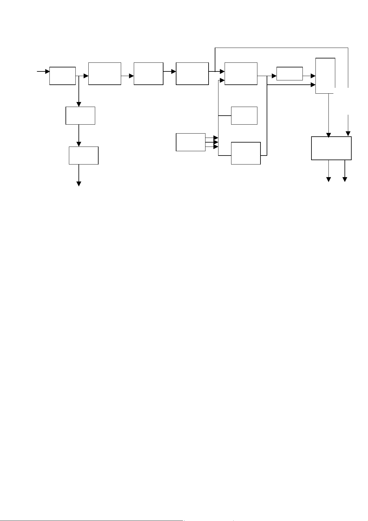
L-track signal is sent by coupling of R101, R103 and C101 to B-pole of differential
amplification stage V102. V102 and V103 compose of differential amplification circuit of
single-end input and output. Speech signal is outputted from C-pole of V102 to B-pole of
voltage amplification stage V105, and then to compound power amplification stage after
amplifying voltage. V104, V107, VD102 and VD103 compose of image constant-current
source circuit. VD102 and VD103 provide constant base current for V104 and V107. The
emitter resistance of V104 defines the working current of differential amplification stage
and the emitter resistance of V107 decides the working current of voltage amplification
stage. V132 and V112 compose of compound tube amplification, making the final stage of
power amplification with strong current amplification, which compose of wave plus
half-circle amplification. V133 and V113 compose of wave minus half-circle amplification,
whose circuit structure is completely the same to the previous tube. Two functions of
temperature compensation tube V106 are: firstly, it is the base-level bias of upper and
lower tubes. Its working status determines the static working current of compound power
amplification. That is, we can set the static working point of compound power
amplification stage by adjusting V106 conduction. The common way is to change the base
resistance of V107. It can also automatically adjust the working status of compound power
amplification stage when the temperature arises. The adjusting process is:
Total current of output stage = working current + leakage current
When temperature arises, leakage current also arises, causing the static working point flow
(bad). At the same time, the leakage current of V106 arises and Uce decreases, causing the
bias current of output stage decreases, working status changes and working current of back
pole decreases, in order to compensate temperature.
Voltage negative feedback is introduced in power amplification circuit of AV215T (RU),
composing of R121, R109 and C105, stabilizing the static working point of differential
stage. AV215T (RU) adopts direct output. R111 and C116 of its output end compose of
Zobel Filter, preventing high-frequency self-excitation caused by A/C inductive reactance
of loudspeaker speech coil.
S
eaker
Ⅱ. The principle of R-track is same to that of L-track. No more words here.
Page 16

Ⅲ. Mute circuit: when pressing mute key of remote controller, a photoelectric conversion
h
p
t
mute signal by remote receiving head is sent to CPU, whose pin 35 and 36 emit a
high-level mute instruction to conduct V115, V101 and V116 and L and R-track signal
short pass ground, achieving the mute control.
Ⅳ. C, SR and SL power amplification circuit: Compared with previous machines, these
three tracks of AV215T (RU) adopt special power amplification LM1876 and IC LM1875.
LM1876 has 15 pins. The pin 2, 15 and 4 are respectively its plus-minus power pins. The
pin 7/8/12/13 are its co-phase and inverse input ends. The rated output power of each track
of the power IC can reach 20W with automatic mute function when starting up. 1875, five
pins, is a power amplification IC with better performance and extremely simple application
circuit which has 15W power output in rated status. Its pin 5 and 3 is plus-minus power
supply pin.
V. Protective circuit
The protective way of L, R and C tracks is to cut off relay Y100 when starting up to cut off
its output. SR and SL tracks protect by mute. AV215T (RU) has functions of starting delay
protection, mid-point over-voltage and over-current protection and standby protection.
1. Starting delay response protective circuit: because the circuit is unstable when
starting up and its dash current does great harm to sound box and power
amplification circuit, the delay response protective circuit is set. There are two
steps for starting delay response protective circuit: Firstly, C, L and R. Its working
process is: the A/C of transformer is rectified and filtered by VD113 and C110 to
form a 22V voltage, then R108 charges C115 to inversely breakdown VD111 and
V105 and V104 forward conduct, finally the Y100 responses and delay forms.
Secondly, L and R surround tracks take starting anti-dash protection by following
ways: when the system resets, pin 33 of CPU outputs a high level, passing R164 to
pin 9 and 14 of LM1876 which outputs mute. After machine succeeds in delaying
starting, pin 33 of CPU switches into low level and SL/SR path normally outputs.
2. Mid-point over-voltage protection: the output end of each track is connected with
a SL are respectively R119 and R120. As long as any mid-point voltage of tracks is
over +3.5V or lower than -3.5V, V101 or V102 conducts to decrease their C-pole
voltage, then V103 conducts to finally cut off relay to protect circuit starting.
Each channel is
connected wit
a over-voltage
sampling
resistance
L-channel
is R116
Over +3.5V
Lower than -3.5V
V101 conducts
V102 conducts
C-pole
voltage
decrease
V103
conduct
Cut off relay to
rotect circui
starting
Page 17

3. Over-current and short-circuit protection: output load resistances of L- and
d
n
y
t
R-track are connected with an over-current sampling triode. The sampling tube of
L-track is V114 and load resistance is R126 and R127. The power amplification IC
of other three tracks has functions of over-current protection. As long as
over-current occurs in L-track, the voltage drop of R126 and R127 will rapidly
increase. Once the voltage drop of R129 is over 0.7V, V114 will conducts, and then
V103 conducts and finally relay cuts off to protect circuit starting.
Each channel
is connecte
with a
over-current
sampling
triode
L-channel
is V114
The voltage
drop of R126
and R127
increases
when
over-current
V114co
nducts
C-pole
voltage
decrease
V103
conducts
Cut off rela
to protec
circuit starting
With the same manner, voltage of R159 will be over 0.7V to conduct V129, then
conduct V103 and finally cut off relay to protect loudspeaker.
4. Energy-saving protection: when standby time reaches 10 minutes and still needs
continuing, CPU pin 34 output PRC signal is high level which saturates and conducts
V100 via VD108 and R101, then conducts V103 and finally cuts off relay to save
standby energy.
Maintenance and Repair Flow
Ⅰ. Malfunction Phenomenon: Sound fault
Analysis:Generally, such fault can be checked by signal injection step by step. If the
speaker of any step has no disturbance, there must be problems with this step. In general,
this method should be carried out from rear step to front step. Another method is signal
detection, which is carried out from front step to rear step. If there be no sound with any
step, this step must be the fault point. Specific examine and repair flow for this fault is
showed as follows:
Page 18

No NoN
f
d
f
f
f
r
h
T
No No N
N
N
o microphone
Check C219,C222 to confirm i
there be sound or not
Check circuit for N210 an
microphone
Yes
Check R219 and R220 to confirm i
there be sound or not
Check PKCK, PKDA signal o
PT2315 and CPU
Yes
Check R215T to confirm i
there be sound or not
Check N202 and its power supply
circuit
Yes
Check C245 and C246 to
confirm there be sound or not
Check N203 and its powe
supply circuit
Yes
Base electrode of V104 and V105
is 0.7AV or not?
o
Check if V104 or V105 have
been brokendown or not
Yes Yes
The E-electrode of V103 is hig
level or not?
o
V103 fault
MICDET be high level? PK
be low level?
o
CPU fault
Microphone fault
V200 fault
Page 19

Ⅱ.Fault phenomenon: No spectrum display
N
N
N
N
m
N
NOKN
N
N
N
f
o spectru
If there be any change between high level
and low level on collect electrode of V105
V105 itself and its power supply is
normal or not?
OK
VD118 is normal or not?
OK
102B forward terminal
voltage jump or not?
102B reversal has high
level and low level or not?
Y
Check CPU and
2
C bus
I
Check power supply, V105
and peripheral circuit
Replace
VD118
Check the circuits
with V103 and V104
Check N102 and
peripheral circuit
OK
108 and CPU control pin
work properly or not?
Check control signal, N108
and peripheral circuit
OK
Check the auto-gain regulation circuit made o
seven-segment band-pass filter, C115 and N105
Page 20

Ⅲ. Fault phenomenon:Automatic search fault
h
N
d
d
N
y
d
N
N
d
Automatic searc
fault
DISPLAY signal be delivered to
103A reversal or not?
Y
Voltage be supplied to N103B
reversal or not?
Y
Co-phased terminals of N103B
are low level or not?
Y
VD103 be normal or not?
Y
Check spectrum sampling an
amplifying circuit, N103 an
Check N103A amplifying
circuit and power suppl
Check N102 an
peripheral circuit
Replace VD103
Check VD101, CPU, V101 an
peripheral circuit
Page 21

Ⅳ. Starting up protection
d
t
Y
Check if there is Mid-Point Voltage or not?
Check which sound track outpu
DC and check this sound track
N
Check if signal or main volume should be
Y
augmented for protection
Check if overcurrent protect diode or triode is
damaged, or capacitor C115 is
poor
N
Check if resistance R111 an
N Y
R141 are open circuit
Replace resistance
Check if resistance R108 is
open circuit
N Y
Check if RLY inspecting signal
works properly
Replace resistance
Check if resistance R201 is
N Y
Y
Vibration protection or not?
open circuit on CPU board
Replace relay
Page 22

R130 1K
TUNER_R
R132 47K
R152 47K
R197 1K
TUNER_L VCD-L
R111 1K
XC101A
3
R112 47K
R
2
XC101B
XC102A
XC102B
XC102C
R113 47K
1
R114 1K
L
R115 1K
6
R116 47K
R
5
R117 47K
4
R118 1K
L
R119 1K
3
R120 47K
R
2
R121 47K
1
R122 1K
L
R103 1K
6
R104 47K
R
5
R105 47K
4
R106 1K
L
R107 1K
9
R108 47K
R
8
R109 47K
7
R110 1K
L
N104B
6
4558
7
5
C105
221
C107
-12V
47u/16V
N104A
2
4558
1
3
C108
C106
47u/16V
221
8 4
+12V
VCD
DVD
R
L
SR
SL
SW
C
R1241KR125
R137 56K
R138 56K
R139 100K
C109 101
R140 47K
R141 22K
R142 33K
220/0.5W
XS22
1
2
P_CLK
3
P_DATA
4
P_LT62446
5
6
7
8
+12V
9
-12V
CON5
XS19
9
8
7
6
5
+12V
TUNER_L
4
3
TUNER_R
2
1
CON8
R174
47K
R175
47K
R176
47K
R177
47K
R178
47K
XS20
SR1
1
SL1
2
C-1
3
R-1
4
L-1
5
SW1
6
7
8
DISP
9
OK-R
10
CON10
+12V
R129
VD100
6.8V
C103 47n
R131
220/0.5W
VD101
C104
6.8V
47u/16V
N101
CD4052
12
X0
14
VCD-R
15
DVD-R
11
5.1CH-R
DVD-L
5.1CH-L
B
B
10
A
A
12
S-C
13
5.1CH-C
S-SR
5.1CH-SR
S-SL
5.1CH-SL
11
10
5.1CH
5.1CH
12
13
SW
11
10
LR-T
R195
R126
56K
1K
1K
2
3
R143
27K
6
5
13
X1
X
X2
X3
3
Y
1
Y0
5
Y1
2
Y2
4
16
A+6.8V
Y3
VDD
6
INH
8
VSS
9
B
7
A-6.8V
VEE
A
N102
CD4053
14
X0
X
X1
2
15
Y0
Y
1
Y1
5
4
Z0
Z
3
Z1
16
VDD
6
2
1
5
3
6
C110 101
A+6.8V
INH
8
A
Vss
B
7
C9VEE
A-6.8V
R134
R135
R136
150K
150K
N103
CD4053
14
X0
X
X1
15
Y0
Y
Y1
4
Z0
Z
Z1
16
VDD
A+6.8V
INH
8
A
Vss
B
7
C9VEE
A-6.8V
S-C
-12V
N105A
C111
4558
1
4.7u/16V
8 4
+12V
N105B
4558
7
S-SR S-SL
150K
R133
150K
R149 22K
R148 30K
R144 47K
R145 22K
R146 33K
C142
47u/16V
822
SR1
SL1
C-1
R-1
L-1
L101 100uH
C141
101
A-6.8V
C132
47u/16V
C148
103
C102 47n
C140
101
D+5V
R163 100
R164 100
R165 100
C139
101
-12V
A-6.8V A +6.8V
C101
47u/16V
R156
R155
R154
R153
22K
22K
22K
22K
1
B
B
A
A
LR-T
LR-T
A+6.8V
C115
47u/16V
C113
221
R150 22K
-12V
N107A
2
4558
3
8 4
+12V
C112 101
R147
27K
N107B
6
4558
5
5.1CH
5.1CH
C116
47n
R157
100K
R160
100K
R161
100K
R162
100K
R158
100K
R159
100K
1
7
R167
100K
R168 27K
R191
100K
C124
15n
C125
0.33u
2
3
4
5
6
C117
4.7u/16V
7
8
C118
4.7u/16V
9
C119
4.7u/16V
10
11
C120
4.7u/16V
12
13
C121
4.7u/16V
14
15
C122
4.7u/16V
16
17
C123
18
822
19
20
R169 68K
C145
10n
OUT4
OUT3
OUT2
OUT1
AVDD
SWIN
GNDS
SRIN
SLIN
GNDC
CIN
GNDR
RIN
GNDL
LIN
BYPASR
BYPASL
LTRE
LBASS3
LBASS2
LBASS121RBASS1
R196 100K
C114 22P
6
5
R170 75K
2
3
C143
47n
42
DVDD
41
CLK
40
DATA
39
LATCH
38
DGND
37
AGND
N106
M62446
N108B
4558
C146
3.9n
-12V
N108A
4558
8 4
+12V
C138 4.7u/16V
36
SWOUT
C137 4.7u/16V
35
SROUT
C136 4.7u/16V
34
SLOUT
C135 4.7u/16V
33
COUT
C134 22u/16V
32
ROUT
C133 22u/16V
31
LOUT
30
AVSS
29
CL1
C131 47n
C130
4.7u/16V
28
CL2
27
CR1
C129
4.7u/16V
26
CR2
C128
25
RTRE
24
RBASS3
C127
15n
23
RBASS2
C126
0.33u
22
C144
C149
C150
103
103
103
7
DISP
C147
1
47u/16V
FAN
HEADPHONE
XS23
1
2
3
CON3
Volume Board
LINE OUT
XC100
1
SW-OUT
P_TCE
P_CLK
P_DATA
P_RLY
RLYC
LRM
SCM
R104
22K
P_TCE
P_TDO
P_CLK
P_DATA
P_LT62446
A+5V
+12V
-12V
R100
2
47K
XS9
SWM
1
L1
2
R1
3
C1
4
SL1
5
SR1
6
7
From AMP Board
CON7
XS13
1
P_RLY
2
RLYC
3
LRM
4
SCM
5
CON5
VD100
1N4148
VD101
1N4148
DIST
DIST
VD103
1N4148
VD104
1N4148
R105
22K
XP22
1
2
3
4
5
6
7
8
9
CON9
C100
R109
1K
BURST
L-1
R-1
C-1
XP20
1
2
3
4
5
6
7
8
9
10
CON10
DISP
OK-R
OK-L
KM
C1-1
XS24
1
2
3
CON3
FAN
HEADPHONE
R170 1
R171 1
SR-1
SL-1
C-1
R-1
L-1
SW1
DISP
OK-R
OK-L
KM
C1-1
VD106 1N4004
VD107 1N4004
22u/16V
C115
R167
4.7K
R168
4.7K
R169 4.7K
BURST
R152 2.2K
9014
R110 1K
R151 2.2K
R153
4.7K
C119
22u/16V
VD108
1N4148
V110
9014
V109
V111
S8050
9014
V107
2N5401
R139
10K
V102
R106
22/0.5W
1000u/16V
R162
10K
+12V
V108
2N5401
V101
S8050
R163
10K
V104
S8050
V103
2N5401
V105
S8050
R143
10K
N107 7805
1
Vin
C130
C128
47n
10u/16V
V100
R115
100K
S8050
C101
R116
100K
10u/16V
R118
100K
D+5V
3
Vout
GND
C129 47n
C134
220u/16V
2
C142 100u/16V
D+5V
C143
C144
47n
47n
C103 47P
R120 22K
R132 27K
N100B
R127 39K
4558
6
5
R128 22K
R122 39K
6
5
R129 20K R124 12K
6
5
+12V +12V
C124
47u/16V
C125
47u/16V
C105 47P
R133 27K
C107 47P
R134 22K
C113
7
4.7u/16V
N101B
4558
C114
7
4.7u/16V
N102B
4558
C118
7
4.7u/16V
C121
47n
C122
47n
-12V-12V
R121 22K
R137 12K
R123 22K
R140 12K
R108 7.5K
R158
220
R161
220
C104 47P
R101 43K
-12V
N100A
4558
2
1
3
8 4
C106 47P
R102 43K
2
3
8 4
C108 47P
R103 47K
2
3
8 4
R1
C13110u/16V
+12V
-12V
N101A
4558
1
L1
C13210u/16V
+12V
R111 4.7K
-12V
N102A
4558
1
+12V
R112 4.7K
C1
R142 47K
R145 47K
SR1
SL1
P_TDO
P_LT62446
C137
C135
103
C138
103
103
Signal Processing Board(一)
Page 23

MIC-DET
8
5
0
7
7
MIC1
GND
GND
XS25
1
2
3
4
5
CON5
XS12
1
2
3
4
CON4
HEADPHONE
P_LT4094
P_DATA
P_CLK
D+5V
DGND
R-1
L-1
HEADPHONE
C217
10u/16V
R243
10K
HEADPHONE
R207 5.1K
+12V
1
-12V
A+5V
C207 47u/ 16V
103
2
P_REM
3
P_D0
4
P_D1
5
P_D2
6
P_D3
7
P_D4
8
P_D5
9
P_D6
10
P_D7
11
P_RST
12
P_RS
13
P_MICDET
14
P_E
15
CON15
R228
100K
R244
150K
N209
PT2399
1
16
VCC
F1-I
C250
REF
AG
DG
CLK
VCO
CC1
CC08P1-O
561
15
F1-O
14
F2-O
C251
561
13
F2-I
12
P2-O
C233
0.1u
11
P2-I
10
P1-I
C232
0.1u
9
2
3
4
R258
5
56K
6
C213
7
0.22u
C214
0.22u
D+5V
C200 151
R200 39K
-12V
N201A
4558
2
3
8 4
+12V
P_MICDET
V202
9014
N210 CD4094
1
STR
2
DATA
3
CLK
9
Qs
10
Q`s
8
VSS
15
OUTB
16
VDD
D+5V
N211 CD4094
1
STR
2
DATA
3
CLK
9
Qs
10
Q`s
8
VSS
15
OUTB
16
VDD
D+5V
N207 CD4051
13
X0
R254 15K
14
X1
R218 20K
X215VDD
R223 27K
12
X3
R260 30K
1
X4
R255 36K
5
X5
R262 43K
2
X6
R256 62K
4
X7
R257 120K
+12V
VD200
9.1V
C219 10u/16V
R213 2K
1
10u/16V
4
FAN
Q1
5
LED
Q2
6
Q3
7
BURST
Q4
14
RLYC LRM
Q5
13
Q6
12
Q7
11
Q8
4
Q1
5
Q2
6
Q3
7
Q4
14
Q5
13
Q6
12
Q7
11
Q8
3
XCOM
6
INH
16
+6.8V
8
VSS
7
VEE
-6.8V
11
A(0)
10
B(1)
9
C(2)
C202 47u/16V
R204
100/0.25W
C211
C225
47n
5.6n
C226
5.6n
C208
100u/16V
C236 10P
R240 220K
C252
-12V
N202A
VD201
4558
2
1
3
FAN
BURST
RLYC LRM
R259 1
R215 2K
R272 3.3K
R270 6.8K
R266 8.2K
R271 12K
R261 18K
R269 33K
1N4148
8 4
+12V
VD203
1N4148
VD204
1N4148
VD206
1N4148
VD205
1N4148
R275
10K
N208 CD4051
13
XCOM
X0
14
X1
X215VDD
12
X3
1
X4
5
X5
2
X6
4
X7
1
2
3
4
5
6
7
8
9
INH
VSS
VEE
A(0)
B(1)
C(2)
N200 PT2315
REF
VDD
AGND
TREBL
TREBR
RIN
LOUD_R
NC
LOUD_L
NC10LIN
R209 1K
C205
47u/16V
SCMKM
R265
10K
3
6
16
8
7
11
10
9
20
P_SCL
CLK
19
P_DATA
DATA
18
DGND
17
LOUT
ROUT
BOUT_R
BIN_R
BOUT_L
BIN_L
SCMKM
R220 10K
C221
16
10u/16V
C227
15
68n
C228
14
68n
13
R216
5.6K
12
11
P_OKT
C237
V200
103
9014
R241
47K
+12V
R263
220/0.5W
C212
47n
C206 47u/16V
VD202
5.1V
C239
+6.8V
-6.8V
XS102
P_D0
1
P_D1
2
P_D2
3
P_D3
4
P_D4
5
P_D5
6
P_D6
7
P_D7
8
CON8
P_TDO
N202B
4558
5
7
6
C234
3.9n
R247 3.9K
+12V
R242
R211
330
1K
V201
9014
C231
68n
C240
R246
39K
0.47u/16V
R210
1K
R2482KR249
R202
20K
R230 15K
XS103
P_RST
1
P_RS
2
3
P_E
4
P_REM
5
LED
6
DGND
7
DGND
8
D+5V
9
D+5V
CON9
R231 47K
N203B
4558
6
5
N205
CD4053
12
X0
13
X1
2
Y0
1
Y1
5
Z0
3
Z1
VDD
6
INH
11
A
Vss
10
B
R238
C9VEE
10K
2K
-12V
C247 4.7u/16V
R222 10K
C242
5.6n
C248 4.7u/16V
R221 12K
R284 22K
R224 10K
R232 15K
R264
4.7K
R225 10K
R226 15K
C243 5.6n
C238
103
C249
4.7u/16V
R227
10K
R229
100K
R267 10K
N204B
4558
6
7
5
P_RLY
1
DISP
2
DIST
3
P_OKT
4
P_CLK
5
P_TCE
6
P_LT62446
7
P_LT4094
8
P_SCL
9
P_DATA
10
11
DGND
12
D+5V
13
DGND
14
DGND
15
R233 200K
CON15
R234 200K
R235 200K
7
14
X
15
Y
4
Z
16
R250 2K
8
7
-6.8V
R251 2K
R252 2K
R268 10K
C235
101
-12v
N204A
4558
2
3
8 4
+12v
P_RLY
DISP
DIST
P_CLK
P_TCE
P_LT62446
P_DATA
D+5V
L-1
R-1
+12v
84
N203A
4558
3
1
2
1
C1-1
-12v
R253 10K
C245 4.7u/16V
OK-L
C246 4.7u/16V
OK-R
+6.8V +1 2V
C215
R239
10u/16V
680
C216
R274
10u/16V
680
-6.8V -12V
+12V +12V
C203
47u/16V
C204
47u/16V
+12V
+12V
DGND
DGND
-12V
-12V
R236 510
R273 510
L-1
R-1
C-1
C1-1
OK-L+6.8V
OK-R
C209
47n
C210
47n
-12V-12V
XS6
1
2
3
4
CON4
Signal Processing Board(二)
C135
154
C134
R162
154
R164
R165
10K
13
12
R163
4.7K
C131
R157
683
10K
10
R158
4.7K
103
C128
R152
C143
223
10K
R153
4.7K
C125
R148
103
10K
R149
4.7K
R143
C122
10K
472
R144
4.7K
C145
C119
R138
152
10K
R139
4.7K
C146
103
C116
R133
561
10K
13
12
R134
4.7K
C115
10u/16V
C114
DISPLAY
10u/16V
129
13
0K
128
14
0K
127
15
K
126
12
K
125
1
K
124
5
3K
123
2
2K
4
122
5K
VD114
100K
1K
1N4148
14
N106D
LM324
C132
683
R159
VD113
9
100K
1N4148
8
N106C
LM324
C129
223
R154
100K
-12V
VD112
2
1N4148
1
3
N106A
LM324
C144
4 11
+12V
103
C126
103
R150
VD111
100K
6
1N4148
7
5
N106B
LM324
C123
472
R145
VD110
100K
6
1N4148
7
5
N105B
LM324
C120
152
-12V
R140
100K
103
VD109
2
1N4148
1
3
N105A
LM324
4 11
+12V
C117
561
R135
VD108
100K
1N4148
14
N105D
LM324
R132
10
22K
R131
10K
3
X0
X
X1
16
VCC
X2
8
GND
6
X3
INH
7
X4
VEE
X5
11
X6
A
10
B
9
X7
C
N104
CD4051
35Hz
C136
R166
2.2u/50V
10K
R160
1K
134Hz
R161
C133
10K
2.2u/50V
R155
1K
300Hz
R156
C130
10K
2.2u/50V
R151
1K
1KHz
R186
C127
10K
2.2u/50V
R146
1K
2.2KHz
R147
C124
10K
2.2u/50V
R141
1K
6.3KHz
R142
C121
10K
2.2u/50V
R136
1K
16KHz
R137
C118
10K
2.2u/50V
N105C
LM324
8
9
R130
470K
R118
+6.8V
C113
470/0.25W
10P
C111
10u/16V
C112
10u/16V
-6.8V
R117
+12V
VD106
10K
6.8V
VD107
6.8V
-12V
R119
P_GNA
470/0.25W
P_GNB
P_GNC
DIST
C139
R180
47K
10u/25V
+12V
C140
100u/16V
C141
100u/16V
-12V
N108
13
14
15
12
C149
103
3
2
3
X0
X
X1
16
VCC
+6.8V
X2
8
GND
6
X3
INH
1
7
X4
VEE
5
2
4
CD4051
84
C150
103
R116
-6.8V
X5
11
P_ADSELA
X6
A
10
P_ADSELB
B
9
P_ADSELC
X7
C
+12V
C110
N103A
4.7u/16V
4558
1
47K
-12V
R115
470k
C151
+12V
84
R181
103
100
3
2
C152
103
-12V
R182
100
R183
22K
+12V
103
C147
+12V
84
4558
N102A
3
R167
2
100K
C148
-12V
103
+5V
N103B
6
5
R114
1.5K
1N4148
4558
7
+12V
R111
R113
4.7K
180K
V102
9014
R112
2.2K
R189
10K
R184
VD119
5.6K
1
N107A
1N4148
4558
+5V
R169
470K
1
R170
1K
R172
10K
R173
5.6K
VD115
VD116
1N4148
1N4148
VD103
C109
2.2u/50V
-12V
P_SELECT
P_DIST
R185
4.7K
D+5V
P_RST
P_RS
P_MICDET
P_E
P_ADSELA
P_ADSELB
P_ADSELC
P_GNB
RESET
P_GNC
P_SELECT
P_ADINT0
P_REM
P_CHARGE
P_DIST
P_SEARCH
P_OKT
R209 22
R210 1M
G100
C103
30P
R187
10K
24.576M
P_KT
+12V
VD117
3.3V
N102B
6
4558
7
5
V103
2N5401
V104
R175
C137
0.1u
R174
4.7K
2.2K
9014
+12V
R110
22K
V101
9014
VD102
R109
1N4148
15K
R107
100
R108
VD101
10K
4.7V
L100
100uH
R203 470
R204 470
R205 470
R206 470
R225 470
R224 470
R223 470
R222 470
R221 470
R207 470
R208 470
R220 470
R219 470
R218 470
R217 470
R216 470
R215 470
R177
1K
C138
0.22u/16V
C102
C100
47u/16V
1
2
3
4
5
6
7
8
9
10
11
12
13
14
15
16
17
18
19
C104
30P
VD118
1N4148
104
L101
RH-357508
N100
SM79164
P10(T2)
P11(T2)
P00(AD0)
P12
P01(AD1)
P13
P02(AD2)
P14
P03(AD3)
P15
P04(AD4)
P16
P05(AD5)
P17
P06(AD6)
RST
P07(AD7)
P30(RXD)
EA/Vpp
P31(TXD)
P32(INT0)
P33(INT1)
P27(A15)
P34(T0)
P26(A14)
P35(T1)
P25(A13)
P36(WR)
P24(A12)
P37(RD)
P23(A11)
XTAL2
P22(A10)
XTAL1
P21(A9)
GND20P20(A8)
+5V
R179
10K
P_ADINT0
V105
9014
R178
10K
P_CHARGE
+5V
C155
C142
103
104
40
Vcc
R231470
39
38
37
36
35
34
33
32
31
10K
30
ALE
29
PSEN
28
27
26
25
24
23
22
21
P_SCL
P_SDA
012345678
R230470
R229470
R228470
R227470
R202470
R201470
R200470
R212
R226470
R199470
R195470
R196470
R192470
R191470
R198470
R197470
R213
10K
+5V
+5V
C108
104
RR100
8*4.7K
P_D0
P_D1
P_D2
P_D3
P_D4
P_D5
P_D6
P_D7
P_GNA
P_RLY
P_CLK
P_SCART
P_LT4094
P_LT62446
P_SCL
P_SDA
R214
10K
+5V
N101
8
VDD
7
TEST
6
SCL
5
24C02
R+5V
R100
R101
P_SEARCH
C105
RESET
V100
9014
22K
4.7K
103
R211
C106
4.3K
4.7u/16V
P_RLY
1
DISP
2
DIST
3
P_OKT
4
P_CLK
5
P_SCART
6
P_LT62446
7
P_LT4094
8
P_SCL
9
P_SDA
10
11
DGND
12
D+5V
13
DGND
14
DGND
15
CON15
XP100
+12V
1
-12V
2
P_REM
3
P_D0
4
P_D1
5
P_D2
6
P_D3
7
P_D4
8
P_D5
9
P_D6
10
P_D7
11
P_RST
12
P_RS
13
P_MICDET
14
P_E
15
CON15
R104
1
A0
0
2
A1
3
A2
VSS4SDA
C107
104
Page 24

CON8
R
22n
XP105
CON8
CPU Board
P_RST'
1
P_RS'
2
3
P_RE'
4
P_D0'
5
P_D1'
6
P_D2'
7
8
P_D3'
1
P_D4'
2
P_D5'
3
P_D6'
4
P_D7'
5
+3V3
6
7
8
C105
R107
R100
473
S8050
1
VD100
LED
V100
C100
C101
220
N102 74VHC245
2
3
4
5
6
7
8
9
1
1
2
3
4
5
6
7
8
9
G100
10
151
11
151
455KHz
A0
B0
A1
B1
A2
B2
A3
B3
A4
B4
A5
B5
A6
B6
A7
B7
E19VCC
DIR
GND
N101 PT2222
KI2
KI3
KI4
KI5
KI6
KI7
REM
VDD
SEL
OSCO
OSCI
VSS12LMP
KI/O0
KI/O1
KI/O2
KI/O3
KI/O4
KI/O5
KI/O6
KI/O7
18
17
16
15
14
13
12
11
+3V3
20
C102
10
104
24
KI1
23
KI0
22
CCS
21
20
19
18
17
16
15
14
13
XP102
P_D0
1
P_D1
2
P_D2
3
P_D3
4
P_D4
5
P_D5
6
P_D6
7
P_D7
8
CON8
S100
S106
KEY
KEY
S101
KEY
S102
KEY
S103
KEY
S104
KEY
S105
KEY
VD101
S107
1N4148
VD102
KEY
S108
1N4148
KEY
VD103
S109
1N4148
VD104
KEY
1N4148
VD109
S111
1N4148
KEY
S110
P_RST'
P_RS'
P_RE'
N103 74VHC245
2
3
4
5
6
7
8
9
1
18
A0
B0
17
A1
B1
16
A2
B2
15
A3
B3
14
A4
B4
13
A5
B5
12
A6
B6
11
A7
B7
E19VCC
DIR
GND
D+5V +3V3
10
47u/16V
VD105
1N4148
C108
VD108 1N4148
C103
104
1N4148
VD106
VD107
1N4148
C109
103
+3V3
20
R104
15K
C110
47u/16V
R103
V101
9014
C107
47u/16V
D+5V
47
LED
N100
REMOT
R106
1K
XP103
P_RST
1
P_RS
2
3
P_E
4
P_REM
5
LED
6
DGND
7
DGND
8
9
CON9
R101
10K
1
OUT
VS3GND
2
C106
R105
473
4.7K
~220V 50HZ
OVER
P_RC
RLY0
SWM
From AMPFrom AMP
XP8
L2
R2
C2
SL2
SR2
VC+
GND
GND
VC-
CON9
Control Panel
VD100
1N5404
VD101
FL100
XS1
T6.3AL250V
2
1
CON2
XP7
4
3
2
1
CON4
1
2
3
4
5
6
7
8
9
C102
CT7 472
VD108
RLY0
IN4148
SWM
VC+
VC-
XS2
1
TO SWITCH
2
CON2
XS3
1
TO TRANS
2
CON2
VD113
R100
47/3W
1N4004
R102
1K
R101
1K
R103
47K
R111
4.7/1W
R112
4.7/1W
R113
4.7/1W
R114
4.7/1W
R115
4.71W
C116 0.1u
C117 0.1u
C118 0.1u
C119 0.1u
C120 0.1u
R104
10K
V100
C9014
C126
103
L100
0.7UH
L101
0.7UH
R105
10K
V101
C9014
From TRANS
XS4
~V1
0
~V1
V-RLY
CON4
C110
220u/35V
V102
C9014
R116
51K
R117
51K
R118
47K
R119
47K
R120
47K
1
2
3
4
C122
R106
104
4.7K
C113
R109
220u/16V
10k
C114
220u/16V
1
2
XL101A
WP6
FL101
T8AL250V
C103
0.22u
C104
0.22u
FL102
T8AL250V
VD110
IN4148
R108
100K
R107
100K
C115
V103
47U/25V
C9015
C121
103
1
2
XL101A
WP6
C101 22n
C105 22n
C111 22n
VD111
5.1V
9
10
11
12
13 14
Y100
RELAY-4
VD112
1N4148
1N5404
VD102
1N5404
VD103
1N5404
VD104
1N5404
VD105
1N5404
VD106
1N5404
VD107
1N5404
C123
103
C112
103
XL100A
1
2
Vc+
C106
0.1u
C107
0.1u
Vc-
XL100A
1
2
WP4
WP4
V105
C9014
C108
8200u/63V
C109
8200u/63V
R110
56K
XL101A
1
1
5
2
2
6
3
7
4
8
SWM
RLY0
WP6
V104
C8050
Page 25

Power Board
C103
47u/100V
R1052KR106
47u/100V
V102
2N5551
C113
V117
2N5551
C104
220p
R107 47
100u/16V
V104
2N5551
R110
C107
47u/100V
R1352KR136
C114
220p
R137 47
100u/16V
V119
2N5551
R140
C117
47u/100V
2K
V103
2N5551
R108
47
R109 1K
C105
VD102
1N4148
510
VD103
1N4148
2K
V118
2N5551
R138
47
R139 1K
C115
VD105
1N4148
510
VD106
1N4148
10K
V101
VD101
1N4148
XP9
SWM
1
L1
2
R1
3
C1
4
SL1
5
SR1
6
GND
7
CON7
XP13
GND
1
P_Rly
2
P_RC
3
P_LRM
4
P_CSM
5
CON5
S8050
R161
4.7K
V115
2N5401
R162
C121
10K
22u/16V
V116
S8050
10u/16V
R104
R102
47K
100K
R131
10K
C111
R133
1K
10u/16V
R134
R132
47K
100K
C101
R103
R101
1K
Vs+
R163
10K
R164
33K
C124
R167
4.7K
R165
4.7K
C122
22u/16V
R166
4.7K
C123
22u/16V
10u/16V
R169
V131
2K
S8050
V130
2N5401
R168
C125
22u/16V
10K
Vs+
C127
53
47n
1
4
2
N104
LM1875
R171
24K
R170
820
C128
C126
68p
47n
Vs-
33p/500V
R111
33K/0.5W
33p/500V
R141
33K/0.5W
2N5551
R112
2N5551
R142
C108
R114 2.7K
V106
R115
1.2K
1K
C118
R144 2.7K
V121
R145
1.2K
1K
R117
220/0.5W
V132
R113
2SC5248
150
V105
2N5401
2N5551
R116
R143
2N5401
R146
V107
150
150
V120
V122
2N5551
150
220/0.5W
220/0.5W
220/0.5W
100/0.25W
R121
C109
33K
47n
100/0.25W
V133
2SA1964
R125
R147
V134
2SC5248
100/0.25W
R151
C119
33K
47n
100/0.25W
V135
2SA1964
R155
1u/50V
C158
471
C157
471
Vc+
V112
2SD1047C
R128
4.3K
R126
R129
R120
0.25/7W
2.7K
R122
R127
0.25/7W
R130
4.3K
V113
2SB817C
Vc-
Vc+
V127
2SD1047C
R158
4.3K
R156
R159
R150
0.25/7W
2.7K
R152
R157
0.25/7W
R160
4.3K
V128
2SB817C
Vc-
C130 1u/50VC129
22u/16V
R172 47K
VD104
1N4148
V114
2N5551
C110
1u/16V
N101
C146
L7812
220u/25V
R183
1
Vs+
VD107
1N4148
V129
2N5551
C120
1u/16V
C155 47p R182 33K
N105
R173 1K
LM1876
R174
820
7
8
6
MUTEA
11
MUTEB
9
STAN-A
14
STAN-B
R177
1K
13
12
R178
820
C131
R176
47K
C132
22u/16V
Vs-
R175
30K
3
OUTA
A
C134
104
2
VDDA
5
GNDA
15
VDDB
C135
10
GNDB
4
VEE
C136
104
OUTB
1
B
R179
30K
Vin
22/3W
R184
2
Vin
30/2W
C147
N102
220u/25V
L7912
Vs+
Vs+
10u/100V
104
Vs-
C148
100u/16V
3
Vout
Vout
C141
C142
4700u/35V
3
100u/16V
C150
47n
C151
47n
C149
VD111
1N5404
VD112
1N5404
VD113
1N5404
VD114
1N5404
GND
2
1
GND
C139
47n
4700u/35V
C159
C140
47n
FL101
T6.3A250V
FL102
T6.3A250V
XS7
SWM
1
Rly0
2
P_RC
3
Over
4
CON4
XP6
+12V
1
DGND
2
DGND
3
-12V
4
CON4
XS8
L2
1
R2
2
C2
3
SL2
4
SR2
5
6
Vc+
GND
7
8
9
Vc-
CON9
XS5
C143
0.1u
1
2
3
C144
CON3
0.1u
Power-amplificati on Board and Protective Circuit
 Loading...