

Page 1
SERVICE MANUAL
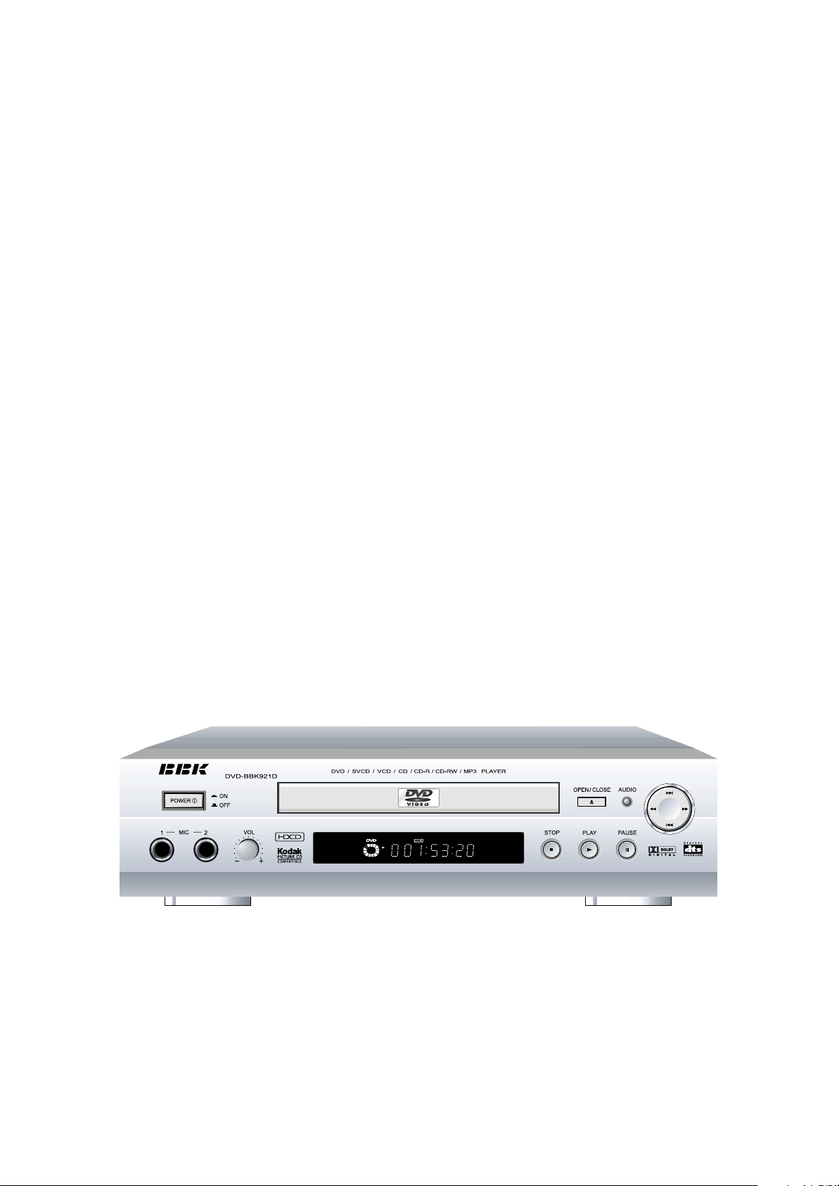
BBK921D
Page 2

CONTENTS
1. SAFETY PRECAUTIONS
1.1 GENENRAL GUIDELINES
2. PREVENTION OF ELECTRO STATIC DISCHARGE(ESD)TO ELECTROSTATICALLY
SENSITIVE(ES) DEVICES
3. PRECAUTION OF LASTER DIODE
4. GENERAL DESCRIPTION
5. PREVENTION OF STATIC ELECTRICITY DISCHARGE
5.1 GROUNDING FOR ELECTROSTATIC BREAKDOWN PREVENTION
5.1.1 WORKTABLE GROUNDING
5.1.2 HUMAN BODY GROUNDING
5.1.3 HANDING OF OPTICAL PICKUP
5.2 HANDING PRECAUTIONS FOR TRAVERSE UNIT(OPTICAL PICKUP)
6. ASSENBLING AND DISASSEMBLING THE MECHANISM UNIT
6.1 DISASSEMBLY PROCEDURE
6.2 TERMINAL PCB
6.3 CLAMP PLATE UNIT
6.4 TRAY
2
2
2
3
4
6
6
6
6
6
6
7
7
7
8
8
6.5 TRAVERSE BLOCK
6.6 TRAVERSE GEAR
6.7 OPTICAL PICKUP UNIT
6.7.1 PRECAUTIONS IN OPTICAL PICKUP REPLACEMENT
6.8 DISASSEMBLING THE MIDDLE CHASSIS
6.9 DISASSENBLING THE TRAVERSE GRAR A
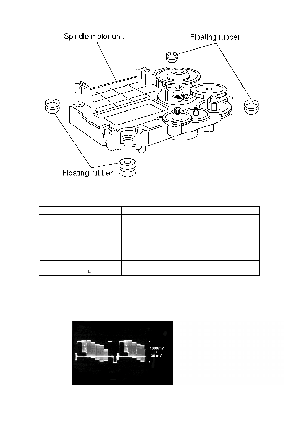
6.10 DISASSEMBLING THE SPINDLE MOTOR UNIT
7. ELECTRICAL CONFIRMATION
7.1 VIDEO OUTPUT(LUMINANCE SIGNAL)CONFIRMATION
7.2 VIDEO OUTPUT(CHROMINANCE SIGNAL)CONFIRMATION
8. MPEG CHECK WAVEFORM
9. IC BLOCK DIAGRAM & DESCRIPTION
10. SCHEMATIC & PCB WIRING DIAGRAM
11. SPARE PARTS LIST
9
9
10
10
12
12
13
13
13
14
15
16
32
45
1
Page 3

1.SAFETY PRICAUTIONS
1.1 GENERAL GUIDELINES
1.When servicing,observe the original lead dress.ifa short circuit is found,replace all parts which have
been overheated or damaged by the short circuit.
2.After servicing,see to it that all the protective devices such as insulation bamiers,insulation papers
shields are properly installed.
3.After servicing,make the following leakage current checks to prevent the customer from being exposed
to thock hazards.
2.PREVENTION OF ELECTRO STATIC DISCHARGE(ESD) TO ELECTROSTATECALLY
SENSITIVE(ES) DEVICES
Some semiconductor(solid state)devices can be damaged easily by static electricity.Such components
commonly are called Electrostatically Sensitive(ES)Devices.Examples of typical ES devices are integrated
circuits and some field-effect transistorsand semiconductor chip components.The following techniques
should be used to help reduce the incidence of component damage caused by electro static discharge(ESD).
1.Immediately before handling any semiconductor component or semiconductor-equipped assembly,drain
off any ESDon your body by touching a known earth ground.Alteatively,obtain and wear a commercially
availabel discharging ESD wrist strap,which should be removed for potential shock reasons prior to
applying power to the unit under test.
2.After removing an electrical assembly equipped with ES devices,place the assembly on a conductive
surface such as alminum foil,to prevent electrostatic charge buildup or exposure of the assembly.
3.Use only a grounded-tip soldering iron to solder or unsolder ES devices.
4.Use only an anti-static solder removal device.Some solder removal devices not classified as anti-static
(ESD protected)can generate electrical charge sufficient to damage ES devices.
5.Do not use freon-propelled chemicals.These can generate electrical charges sufficient to damage ES
devices.
6.Do not remove a replacement ES device from its protective package until immediately before you are
ready to install if.(Most replacement ES devices are packaged with leads electrically shorted together by
conductive foam,alminum foil or comparable conductive material).
7.Immediately before removing the protective material from the leads of a aeplacement ES device,touch
the protective material to the chassis or circuit assembly into which the device will be installed.
Caution
Be sure no power is applied to the chassis or circuit,and observe all other safety precautions.
8.Minimize bodily motions when handling unpackaged replacement ES devices.(Otherwise hamless motion
such as the brushing together of your clothes fabric or the lifting of your foot from a carpeted floor can
generate static electricity(ESD)
notice (1885x323x2 tiff)
2
Page 4
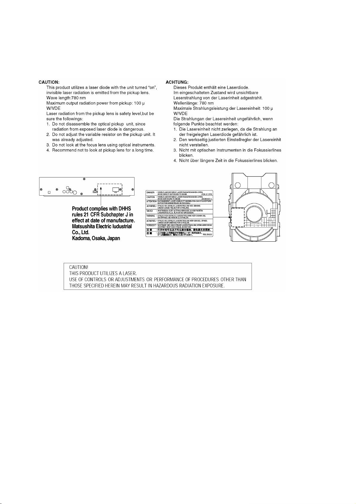
3. Precaution of L aster Diode
3
Page 5
4
Page 6
5
Page 7
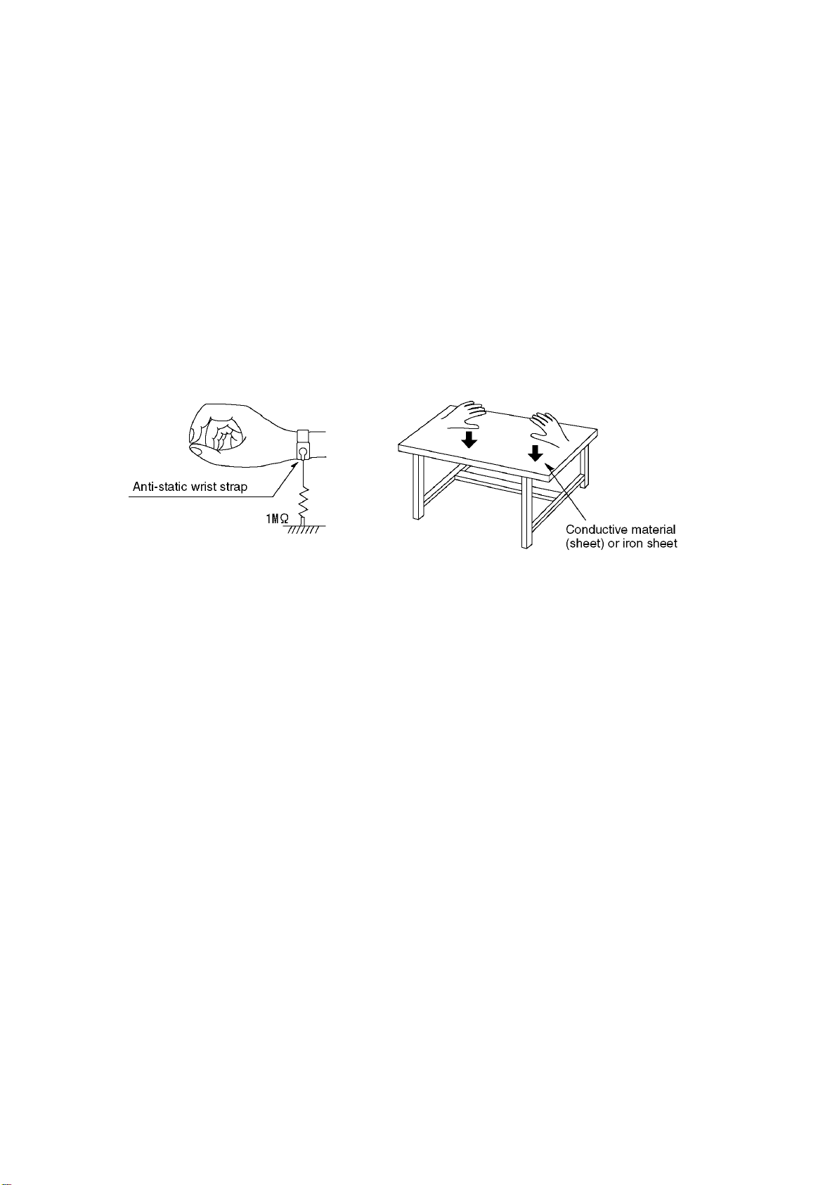
5.PREVERTION OF STATIC ELECTRICITY DISCHARGE
The laser diode in the traverse unit (optical pickup)may brake down due to static electricity of clothes or human
Some devices such as the DVD player use the optical pickup(laser diode)and the optical pickup will be damaged
by static electricity in the working environment.Proceed servicing works under the working environment where
1.Put a conductive material(sheet)or iron sheet on the area where the optical pickup is placed,and ground thesheet.
3.The flexible cable may be cut off if an excessive force is applied to it.Use caution when handling the cable.
6
body.Use due caution to electrostatic breakdown when servicing and handling the laser diode.
5.1.Grounding for electrostatic breakdown prevention
grounding works is completed.
5.1.1. Worktable grounding
5.1.2.Human body grounding
1 Use the anti-static wrist strap to discharge the static electricity form your body.
safety_3 (1577x409x2 tiff)
5.1.3.Handing of optical pickup
1.To keep the good quality of the optical pickup maintenance parts during transportation and before
installation,the both ends of the laser diode are short-circuited.After replacing the parts with new ones,
remove the short circuit according to the correct procedure.(See this Technical Guide).
2.Do not use a tester to check the laser diode for the optical pickup .Failure to do so willdamage the laser
diode due to the power supply in the tester.
5.2.Handing precautions for Traverse Unit (Optical Pickup)
1.Do not give a considerable shock to the traverse unit(optical pickup)as it has an extremely high-precise
structure.
2.When replacing the optical pickup,install the flexible cable and cut is short land with a nipper.See the
optical pickup replacement procedure in this Technical Guide.Before replacing the traverse unit,remove
the short pin for preventingstatic electricity and install a new unit.Connect the connector as short times as
possible.
4.The half-fixed resistor for laser power adjustment cannot be adjusted.Do not turn the resistor.
Page 8
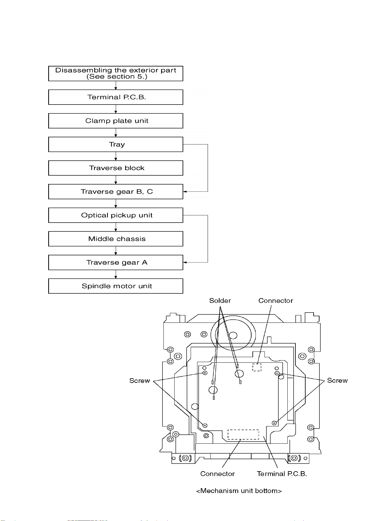
6.ASSEMBLING AND DISASSENBLING THE MECHANISM UNIT
7
6.1Disassembly Procedure
6.2 Terminal P.C.B.
1.Unscrew the screws.
2.Remove the solders.
3.Remove the connectors
5
Page 9

6.3 Clamp Plate Unit
8
1.Spread the stopper with hand to silde the tabs and remove the clamp plate unit.
6.4 Tray
1.Lift the tray.
6
Page 10

6.5 Traverse Block
9
1.Lift the traverse block while spreading the hook of the mechanical chassis chassis unit.
2.Disengage the tabs from the holes of the mechanical chassis unit.
6.6. Traverse Gear
1.Disengage the tabs from the traverse gear
2.Remove the traverse gears B and C.
7
Page 11

5.6 Mechanism Unit
10
1.Unscrew the screws.
2.Remove the connectors.
6.7 Optical Pickup Unit
1. Unscrew the screws.
5.7 Terninal P.C.B.
2.Remove the spring holders and the springs.
3.Pull out of the drive shaft and guide shaft.
1.Unscrew the screws
2.Remove the solders.
3.Remove the connectors.
Page 12
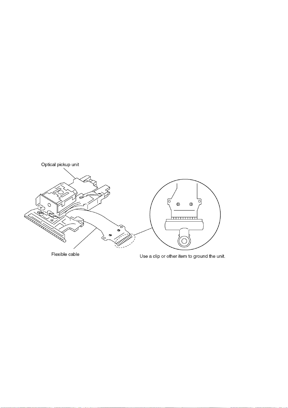
The optical pickup can be damaged by static electricity from you body.Be sure to take static electricity countermeasures
when working around the optical pickup.(Refer to the related page in this Manual about the countermeasures.
3.The use of soldering iron with anti-static feature is recommended when providing short-circuit to laser diode or when
-When using the soldering iron without anti-static feature,short-circuit the flexible cable terminal with a clip before
6.7.1. Precautions in optical pickup replacement
11
1.Do not touch laser diode,actuator and their peripheries.
2.Do not use tester to check laser diode.(Laser diode can be damaged easily.)
removing it.
4.Solder the land on flexible cable of optical pickup unit.
Page 13
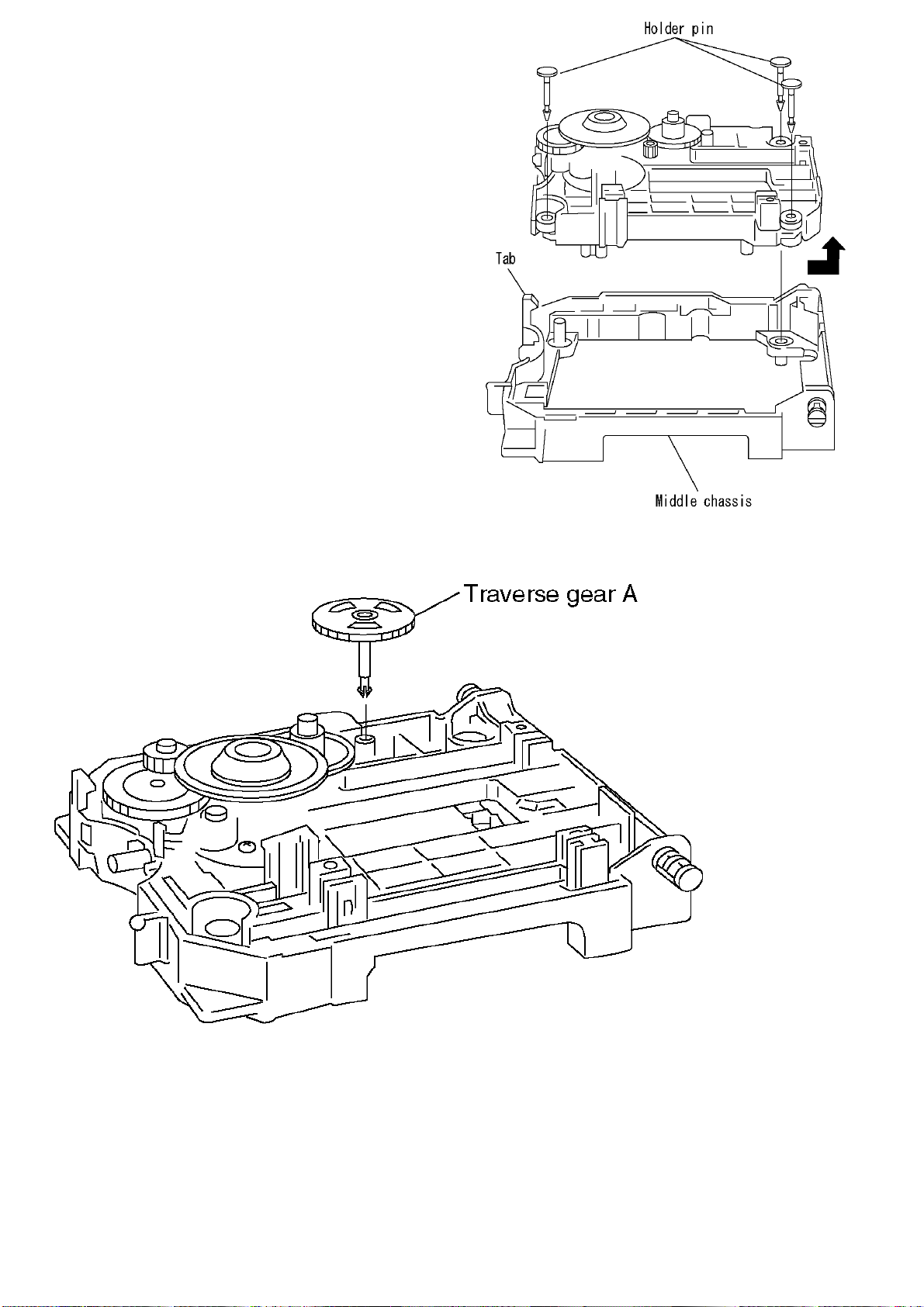
6.8. Disassenbling the Middle Chassis
12
1.Remove the holders pins.
2.Remove the tab.
3.It lifts while pulling it in the direction of the arrow.
6.9. Disassenbling the Traverse Gear A
1.Remove the traverse gear A.
Page 14
7. Electrical Confirmation
13
7.1. Video Output (Luminance Signal) Confirmation
DO this confirmation after replacing a P.C.B.
Measurement point
Mode Disc
Color bar 75%
Video output terminal
Measuring equipment,tools
200mV/dir,10 sec/dir
Purpose:To maintain video signal output compatibility.
1.Connect the oscilloscope to the video output terminal and terminate at 75 ohms.
2.Confirm that luminance signal(Y+S)level is 1000mVp-p±30mV
PLAY(Title 46):DVDT-S15
PLAY(Title 12):DVDT-S01
Confirmation value
1000mVp-p±30mV
DVDT-S15
or
DVDT-S01
Page 15

7.2. Video Output (Chrominance Signal) Confirmation
Screwdriver,Oscilloscope
141
Do the confirmation after replacing P.C.B.
Measurement point
Mode Disc
Color bar 75%
Video output terminal
Measuring equipment,tools Confirmation value
200mV/dir,10 sec/dir
Purpose:To maintain video signal output compatibility.
1.Connect the oscilloscope to the video output terminal and terminate at 75 ohme.
2.Confirm that the chrominance signal(C)level is 621 mVp-p±30mV
PLAY(Title 46):DVDT-S15
PLAY(Title 12):DVDT-S01
621mVp-p±30mV
DVDT-S15
or
DVDT-S01
Page 16

8.MPEG BOARD CHECK WAVEFORM
2. IC5L0380R PIN.2 WAVEFORM DIAGRAM
1. 27MHz WAVEFORM DIAGRAM
15
Page 17

PRELIMINARY
16
ES60X8 PINOUT DIAGRAM
The identical device pinouts for the ES6008, ES6018, ES6028
and ES6038 are shown in Figure 2.
HIOCS16#/CAMCLK/AUX3[4]
HA1/AUX4[3]
VSS
VEE
HA2
/AUX4[4]
VEE
AUX[0]
AUX[1]
AUX[2]/IOW#
VSS
VEE
AUX[3]/IOR#
AUX[4]
AUX[5]
AUX[6]
AUX[7]
LOE#
VSS
VCC
LCS0#
LCS1#
LCS2#
LCS3#
VSS
LD0
LD1
LD2
LD3
LD4
VEE
VSS
LD5
LD6
LD7
LD8
LD9
LD10
LD11
VSS
VEE
LD12
LD13
LD14
LD15
LWR LL#
LWRHL#
VSS
VEE
CAMIN0
CAMIN1
LA0
LA1
LA2
LA3
VSS
HA0/AUX4[2]
154
155
156
157
158
159
160
161
162
163
164
165
166
167
168
169
170
171
172
173
174
175
176
177
178
179
180
181
182
183
184
185
186
187
188
189
190
191
192
193
194
195
196
197
198
199
200
201
202
203
204
205
206
207
208
1
2 3 4 5 6 7 8 910111213141516171819202122232425262728293031323334353637383940414243444546474849505152
HWR#/DCI_CLK/AUX4[5]
HRD#/DCI_ACK#/AUX4[6]
HCS3FX#/AU X 3[6]
153
VEE
HCS1FX#/AU X 3[7]
152
VSS
HIORDY/AUX3[3]
HIRQ/DCI_ERR#/AUX4[7]
HRST#/AUX3[5]
HRRQ#/AUX4[0]
143
144
145
146
147
148
149
150
151
VSS
HD13/AUX2[5]/SP
HD12/AUX2[4]/C2PO
HD11/AUX2 [3]//IRQ
HD10/AUX2[2]/SQSK
HWRQ#/DCI_REQ#/AUX4[1]
HD15/A UX2[7]/IR
HD14/AUX2[6]/SQSI
VCC
138
139
140
141
142
HD9/AUX2[1]/SQSO
133
134
135
136
137
ES6008/18/28/38
208-Pin PQFP Package
HD8/DCI_FDS#/AUX2[0]/VFD_CLk
132
ES6008/18/28/38 DATA SHEET
ES60X8 PINOUT DIAGRAM
HD4/DCI4/AUX1[4]
HD5/DCI5/AUX1[5]
HD6/DCI6/AUX1[6]/VFD_DOUT
HD2/DCI2/AUX1[2]
HD3/DCI3/AUX1[3]
VSS
HD7/DCI7/AUX1[ 7 ]/VFD_DIN
VEE
128
129
130
131
HD1/DCI1/AUX1[1]
HD0/DCI0/AUX1[0]
VCC
VSS
HSYNC#/CAMIN7/AUX3[0]
PCLK2XSCN/CAMIN4
YUV7/CAMIN3
YUV6/VDAC
PCLKQSCN/CAMIN5/AUX3[2]
VSYNC#/CAMIN6/AUX3[1]
118
119
120
121
122
123
124
125
126
127
YUV5/YDAC
VSS
ADVEE
YUV4/RSET
YUV3/COMP
YUV2/CDAC
YUV1/VREF
YUV0/CAMIN2/UDAC
DCLK
105
106
107
108
109
110
111
112
113
114
115
116
117
104
103
102
101
100
96
94
93
91
57
99
98
97
95
92
90
89
88
87
86
85
84
83
82
81
80
79
78
77
76
75
74
73
72
71
70
69
68
67
66
65
64
63
62
61
60
59
58
56
55
54
53
VEE
VSS
DSCK
DQM
DCS0#
VEE
VSS
DCS1#
DB15
DB14
DB13
DB12
VEE
VSS
DB11
DB10
DB9
DB8
DB7
DB6
VSS
VCC
DB5
DB4
DB3
DB2
DB1
DB0
VSS
VEE
DMBS1
DMBS0
DRAS#
DWE#
DOE#/DSCK_EN
DCAS#
VEE
VSS
DMA11
DMA10
DMA9
DMA8
DMA7
DMA6
VSS
VEE
DMA5
DMA4
DMA3
DMA2
DMA1
DMA0
VEE
LA4
LA5
LA6
LA7
LA8
LA9
VSS
VCC
VSS
LA11
LA10
LA12
LA13
VEE
LA14
LA15
LA16
LA20
LA17
LA18
LA19
LA21
RESET#
TDMDX/RSEL
VSS
VEE
TDMDR
TDMCLK
VSS
VCC
TDMFS
TDMTSC#
TWS/SEL_PLL2
TSD2
TSD0/SEL_PLL0
TSD1/SEL_PLL1
NC
MCLK
TBCK
SPDIF/PLL3
VSS
TSD3
VCC
RSD
RWS
NC
RBCK
XIN
AVEE
XOUT
VSS
Figure 2 ES60x8 Pinout
SAM0400-100401 ESS Technology, Inc.
Page 18

ES6008/18/28/38 DAT A SHEET
17
PRELIMINARY
ES60X8 PIN DESCRIPTION
ES60X8 PIN DESCRIPTION
Table 1 lists the identical pin descriptions for the ES6008,
ES6018, ES6028 and ES6038.
Table 1 ES60x8 Pin Description
Name Number I/O Definition
VEE 1,18, 27, 59, 68,
75, 92, 99, 104,
130, 148, 157,
159, 164, 183,
193, 201
VSS 8, 17, 26, 34, 43 ,
52, 60, 67, 76,
84, 91, 98, 103,
112, 120, 129,
138, 147, 156,
163, 171, 177,
184, 192, 200,
208
LA[21:0] 23:19, 16:10,
7:2, 207:204
VCC 9, 35, 44, 83,
121, 139, 172
RESET# 24 I Reset input, active low.
TDMDX
RSEL I ROM Select.
25
I I/O power supply.
I Ground.
O Device address output.
I Core power supply.
O TDM transmit data.
RSEL Selection
016-bit ROM
1 8-bit ROM
TDMDR 28 I TDM receive data.
TDMCLK 29 I TDM clock input.
TDMFS 30 I TDM frame sync.
TDMTSC# 31 O TDM output enable.
TWS
O Audio transmit frame sync.
SEL_PLL2 I System and DSCK output clock frequency selection is made at the rising edge of
RESET#. The matrix belo w list s the avai lable c lock freque ncies and their res pective
PLL bit settings.
32
TSD0
SEL_PLL0 I Refer to the description and matrix for SEL_PLL2 pin 32.
33
TSD1
SEL_PLL1 I Refer to the description and matrix for SEL_PLL2 pin 32.
36
O Audio transmit serial data port 0.
O Audio transmit serial data port 1.
SEL_PLL2 SEL_PLL1 SEL_PLL0 Clock Type
0 0 0 VCO off.
0 0 1 DCLK
0 1 0 Bypass mode
0 1 1 DCLK x 2
1 0 0 DCLK x 4.5
1 0 1 DCLK x 3
1 1 0 DCLK x 3.5z
1 1 1 DCLK x 4
TSD[2] 37 O Audio transmit serial data output 2.
TSD[3] 38 O Audio transmit serial data output 3.
ESS Technology, Inc. SAM0400-100401
Page 19

PRELIMINARY
18
Table 1 ES60x8 Pin Description (Continued)
Name Number I/O Definition
MCLK 39 I/O Audio master clock for audio DAC.
TBCK 40 O Audio transmit bit clock.
SPDIF
SEL_PLL3 I Clock source select.
41
NC 42, 48 No connect pins. Leave open.
RSD 45 I Audio receiv e serial data.
RWS 46 I Audio receive frame sync.
RBCK 47 I Audio receive bit clock.
XIN 49 I Crystal input.
XOUT 50 O Crystal output.
AVEE 51 I Analog power for PLL.
DMA[11:0] 66:61, 58:53 O DRAM address bus [11:0].
DCAS# 69 O DRAM column address strobe.
DOE# 70 O DRAM output enable.
DSCK_EN O DRAM clock enable.
DWE# 71 O DRAM write enable.
DRAS# 72 O DRAM row address strobe.
DMBS0 73 O SDRAM bank select 0.
DMBS1 74 O SDRAM bank select 1.
DB[15:0] 96:93, 90:85,
82:77
DCS[1:0]# 97,100 O SDRAM chip select [1:0].
DQM 101 O Data input/output mask.
DSCK 102 O Output clock to SDRAM.
DCLK 105 I 27 MHz clock input to PLL.
YUV0
CAMIN2 I Camera input 2.
UDAC O Video DAC output.
O S/PDIF output.
SEL_PLL3 Clock Source
0 Crystal oscillator
1 DCLK input
I/O DRAM data bus [15:0].
O YUV0 pixel output data.
ES6008/18/28/38 DATA SHEET
ES60X8 PIN DESCRIPTION
Mode YDAC UDAC VDAC CDAC
A Y C Composite C
B Y Composite Composite C
C Y U Composite V
106
DYUCV
Y: Luma component for YUV and Y/C processing.
C: Chrominance signal for Y/C processing.
U: Chrominance component signal for YUV mode.
V: Chrominance component signal for YUV mode.
SAM0400-100401 ESS Technology, Inc.
Page 20

ES6008/18/28/38 DAT A SHEET
19
ES60X8 PIN DESCRIPTION
PRELIMINARY
Table 1 ES60x8 Pin Description (Continued)
Name Number I/O Definition
YUV1 107 O YUV1 pixel output data.
VREF I Internal voltage reference to video DAC. Bypass to ground with 0.1 µF capacitor.
YUV2
CDAC O Video DAC output. Refer to description and matrix for UDAC pin 106.
YUV3 109 O YUV3 pixel output data.
COMP I Compensation input. Bypass to ADVEE with 0.1 µF capacitor.
YUV4 110 O YUV4 pixel output data.
RSET I DAC current adjustment resistor input.
ADVEE 111 I Analog power for video DAC.
YUV5 113 O YUV5 pixel output data.
YDAC O Video DAC output. Refer to description and matrix for UDAC pin 106.
YUV6 114 O YUV6 pixel output data.
VDAC O Video DAC output. Refer to description and matrix for UDAC pin 106.
YUV7 115 O YUV7 pixel output data.
CAMIN3 I Camera YUV 3.
PCLK2XSCN 116 I/O 27-MHz video output pixel clock.
CAMIN4 I Camera YUV 4.
PCLKQSCN 1 17 O 13.5-MHz video output pixel clock.
CAMIN5 I Camera YUV 5.
VSYNC# 118 I/O Vertical sync, active low.
CAMIN6 I Camera YUV 6.
HSYNC# 119 I/O Horizontal sync, active low.
CAMIN7 I Camera YUV 7.
HD[5:0]
DCI[5:0] I/O DVD channel data I/O [5:0].
AUX1[5:0] I/O Aux1 data I/O [5:0].
HD[6]
DCI[6] I/O DVD channel data I/O [6].
AUX1[6] I/O Aux1 data I/O [6].
VFD_DOUT I VFD data output.
HD[7]
DCI[7] I/O DVD channel data I/O [7].
AUX1[7] I/O Aux1 data I/O [7:0].
VFD_DIN I VFD data input.
HD[8]
DCI_FDS# I/O DVD input sector start.
AUX2[0] I/O Aux2 data I/O 0.
VFD_CLK I VFD clock input.
HD[9]
AUX2[1] I/O Aux2 data I/O [1] when selected.
SQSQ I Subcode-Q data.
HD[10]
AUX2[2] I/O Aux2 data I/O [2] when selected.
SQSK I Subcode-Q clock.
108
127:122
128
131
132
133
134
O YUV2 pixel output data.
I/O Host data I/O [5:0].
I/O Host data I/O [6].
I/O Host data I/O [7].
I/O Host data bus 8.
I/O Host data bus line 9.
I/O Host data bus line10.
ESS Technology, Inc. SAM0400-100401
Page 21

PRELIMINARY
20
Table 1 ES60x8 Pin Description (Continued)
Name Number I/O Definition
HD[11]
AUX2[3] I/O Aux2 data I/O [3] when selected.
IRQ O IRQ output.
HD[12]
AUX2[4] I/O Aux2 data I/O [4] when selected.
C2PO I C2PO error correction flag from CD-ROM.
HD[13]
AUX2[5] I/O Aux2 data I/O [5] when selected.
SP I 16550 UART serial port input.
HD[14]
AUX2[6] I/O Aux2 data I/O [6] when selected.
SQSI I Subcode-Q sync.
HD[15]
AUX2[7] I/O Aux2 data I/O [7] when selected.
IR I IR remote control input.
HWRQ#
DCI_REQ# O DVD control interface request.
AUX4[1] I/O Aux4 data I/O 1.
HRRQ# 143 O Host read request.
AUX4[0] I/O Aux4 data I/O 0.
HIRQ
DCI_ERR# I/O DVD channel data error.
AUX4[7] I/O Aux4 data I/O 7.
HRST# 145 O Host reset.
AUX3[5] I/O Aux3 data I/O 5.
HIORDY 146 I Host I/O ready.
AUX3[3] I/O Aux3 data I/O 3.
HWR#
DCI_CLK I/O DVD channel data clock.
AUX4[5] I/O Aux4 data I/O 5.
HRD#
DCI_ACK# O DVD channel data valid.
AUX4[6] I/O Aux4 data I/O 6.
HIOCS16#
CAMCLK I Camera port pixel clock input.
AUX3[4] I/O Aux3 data I/O 4.
HCS1FX# 152 O Host select 1.
AUX3[7] I/O Aux3 data I/O 7.
HCS3FX# 153 O Host select 3.
AUX3[6] I/O Aux3 data I/O 6.
HA[2:0] 158, 155:154 I/O Host address bus.
AUX4[4:2] I/O Aux4 data I/Os [4:2].
AUX[1:0] 160 I/O Auxiliary ports 1:0.
135
136
137
140
141
142
144
149
150
151
I/O Host data bus line11.
I/O Host data bus line12.
I/O Host data bus line13.
I/O Host data bus line14.
I/O Host data bus line15.
O Host write request.
I/O Host interrupt.
I/O Host write.
OHost read.
I Device 16-bit data transfer.
ES6008/18/28/38 DATA SHEET
ES60X8 PIN DESCRIPTION
SAM0400-100401 ESS Technology, Inc.
Page 22

ES6008/18/28/38 DAT A SHEET
21
LICENSING REQUIREMENTS
PRELIMINARY
Table 1 ES60x8 Pin Description (Continued)
Name Number I/O Definition
AUX[2] 162 I/O Auxiliary port 2.
IOW# O I/O Write strobe.
AUX[3] 165 I/O Auxiliary port 3.
IOR# O I/O Read strobe.
AUX[7:3] 169:166 I/O Auxiliary ports 7:3.
LOE# 170 O Device output enabl e.
LCS[3:0]# 176:173 O Chip select [3:0].
LD[15:0] 197:194,
191:185,
182:178
LWRLL# 198 O Device low-byte write enable.
LWRHL# 199 O Device high-byte write enable.
CAMIN0 202 I Camera YUV 0.
CAMIN1 203 I Camera YUV 1.
I/O EPROM device data bus.
LICENSING REQUIREMENTS
Dolby Digital Licensing
Dolby Digital audio enabling softwa re is provid ed with the
Vibrat to seri es of DVD proc essors. Dolby is a tra demark of
the Dolby Labora tories. Supply of th is implementation of
Dolby Technology does not convey a license or imply a
right under any patent, or any other Industrial or
Intellectual Property Ri ght of Dolby Laboratories, to use
this implementation i n any end-user or ready-to -use final
product. Companies planning to us e this implementation
in products must obtain a license from Dolby Laboratories
Licensing Corporation before designing such products.
Additional per-chip royalties may be required and are to be
paid by the purchaser to Dolby Labor atories, Inc. Details
of the OEM Dolby Digital license may be obtained by
writing to:
Dolby Laboratories Inc.
Dolby Laboratories Licensing Corporation
Attn.: Intellectual Property Manager
100 Potrero Avenue
San Francisco, CA 94103-4813
Macrovision Licensing
Macrovision Copy Protection is su pported in the Vibratto
series of DVD processors. The use of Macrovision’s Copy
Protection technology in the device must be authorized by
Macrovision and is intended for home and other limited
pay-per-view uses only, unless otherwise authorized in
writing by Macrovision.
Reverse engineering or disassembly is prohibited. A valid
Macrovision license must be in effect between the Vibratto
purchaser and Macrovision Corporation. Additional perchip royalties ma y be required and are to be paid by th e
purchaser to Macrovision Corporation. Details of the
Macrovision license may be obtained by writing to:
Macrovision Corporation
1341 Orleans Avenue
Sunnyvale, CA 94089
ESS Technology, Inc. SAM0400-100401
Page 23

PRELIMINARY
22
FUNCTIONAL DESCRIPTION
Figure 3 shows the internal block diagram for the basic Vibratto DVD processor.
SRAM
Interface
ESS RISC
Processor
DMA
Controller
Host/ATAPI/UDF
Loader Interface
Serial Audio
Interface
DCI Loader
Interface
MPEG
Decoder
System
Demultiplexer
DVD
Descramble
Interface
2Kx32 ROM
512x32 SRAM
Processor
Video Output
On Screen
Display
Sub-Picture
Decoder
Encoder
Processor
Interface
Host/ATAPI
UDF
Interface
HCS[1,3]FX#
Serial
Audio
Interface
DCI
Interface
LA[21:0]
LCS#[3:0]
LD[15:0]
LWRHL#
LWRLL#
LOE#
HA[2:0]
HD[15:0]
HWRQ#
HRDQ#
HIRQ#
HRST#
HIORDY
HWR#
HRD#
HIOCS16#
RSD
RWS
RBCK
SPDIF
TBCK
MCLK
TSD[3:0]
TWS
DCI_ACK#
DCI_CLK
DCI_ERR#
DCI_REQ#
DCI_FDS#
DCI[7:0]
DRAM
Video
Video
ES6008/18/28/38 DATA SHEET
FUNCTIONAL DESCRIPTION
DSCK_EN
DSCK
DQM
DCS#[1:0]
DMA[11:0]
DWE#
DOE#
DRAS#[2:0]
DB[I5:0]
DCAS#
YUV[7:0]
PCLK2XSCN
PCLKQSCN
VSYNC#
HSYNC#
DRAM
Screen
Display
CDAC
YDAC
UDAC
VDAC
VREF
COMP
RSET
TDM
Interface
TDMCLK
TDMDR
TDMDX
TDMFS
TDMTSC#
TDM
Interface
Registers
Clock
AUX[7:0]
RESET#
XIN
XOUT
Clock,
Aux Ports
and Reset
Figure 3 Vibratto Block Diagram
Vibratto Device Architecture
The Vibratto device architecture includes a RISC
processor, CRT controller, transport mechanism, video
encoder, memory controller, on-screen display (OSD)
controller and video processor.
ESS RISC Processor
Embedded in the Vibratto is a 32-bit data pipelin ed RISC
processor, with a combined 16 kb instruction and data
done mostly in C. Fo r applications involving an external
host processor the communication between a host
processor and the Vibratto is ha ndled by a host inte rface
module. The host interface can also be used for high
speed data input and output.
The ESS RISC processor instruction and data cache
subsystem is organ iz ed as a t wo- way s et a ss ocia tiv e. O n
a cache load-miss and write-miss, the cache lines are
allocated into the cache memory.
cache subsystem. Programming of the RISC processor is
SAM0400-100401 ESS Technology, Inc.
Page 24

2 Megabit (256 K x 8-Bit)
IC BLOCK DIAGRAM & DESCRIPTION
IC U214 Am29F002B/Am29F002NB
23
CMOS 5.0 Volt-only Boot Sector Flash Memory
DISTINCTIVE CHARACTERISTICS
■ Single power supply operation
— 5.0 Volt-only operation for read, erase, and
program operations
— Minimizes system level requirements
■ Manufactured on 0.32 µm process technology
— Compatible with 0.5 µm Am29F002 device
■ High performanc e
— Access times as fast as 55 ns
■ Low power consumption (typical values at
5 MHz)
— 1 µA standby mode current
— 20 mA read current
— 30 mA program/erase current
■ Flexible sector architecture
— One 16 Kbyte, two 8 Kbyte, one 32 Kbyte, and
three 64 Kbyte sectors
— Supports full chip erase
— Sector Protection features:
A hardware method of locking a sector to
prevent any program or erase operations within
that sector
Sectors can be loc k ed v ia pr ogr ammi ng eq uipme nt
T emporary Sector Unprotect feat ure allows code
changes in previously locked sectors
■ Top or bot tom boot blo ck co nfigurations a vaila ble
■ Embedded Algorithms
— Embedded Erase algorithm automatically
preprograms and erases the entire chip or any
combination of designated sectors
— Embedded Program algorithm automatically
writes and verifies data at specified addresses
■ Minimum 1,000,000 write cycle guarantee per
sector
■ 20-year data retention at 125°C
— R eliable operation for the life of the system
■ Package option
— 32-pin PDIP
— 32-pin TSOP
— 32-pin PLCC
■ Compatibility with JEDEC standards
— Pinout and software compatible with
single-power supply Flash
— Super ior inadvertent write protection
■ Data# Polling and toggle bits
— Provides a software method of detecting
program or erase operation completion
■ Erase Suspend/Erase Resume
— Suspends an erase operation to read data from,
or program data to, a sector that is not being
erased, then resumes the erase operation
■ Hardware reset pin (RESET#)
— Hardware method to reset the device to reading
array data (not available on Am29F002NB)
Page 25

PRODUCT SELECTOR GUIDE
IC BLOCK DIAGRAM & DESCRIPTION
24
Family Part Number Am29F002B/Am29F002NB
= 5.0 V ± 5% -55
V
Speed Option
Max access time, ns (t
Max CE# access time, ns (t
Max OE# access time, ns (t
CC
= 5.0 V ± 10% -70 -90 -120
V
CC
)557090120
ACC
)557090120
CE
) 30303550
OE
Note: See “AC Characteristics” for full specifications.
BLOCK DIAGRAM
V
CC
V
SS
RESET#
n/a Am29F002NB
Sector Switches
Erase Voltage
Generator
DQ0
–
DQ7
Input/Output
Buffers
WE#
CE#
OE#
A0–A17
State
Control
Command
Register
VCC Detector
PGM Voltage
Generator
Timer
Chip Enable
Output Enable
STB
Logic
Address Latch
Y-Decoder
X-Decoder
STB
Data
Latch
Y-Gating
Cell Matrix
Page 26

CONNECTION DIAGRAMS
IC BLOCK DIAGRAM & DESCRIPTION
25
RESET#
NC
A16
A15
A12
A7
A6
A5
A4
A3
A2
A1
A0
DQ0
DQ1
DQ2
V
SS
NC on Am29F002NB
1
2
3
4
5
6
7
8
9
10
11
12
13
14
15
16
PDIP
32
31
30
29
28
27
26
25
24
23
22
21
20
19
18
17
V
CC
WE#
A17
A14
A13
A8
A9
A11
OE#
A10
CE#
DQ7
DQ6
DQ5
DQ4
DQ3
A7
A6
A5
A4
A3
A2
A1
A0
DQ0
5
6
7
8
9
10
11
12
13
14
A12
4
15
DQ1
A15
3
DQ2
A16
2
PLCC
17
SS
V
NC on Am29F002NB
RESET#
VCCWE#
31 30
1
32
19 2016
18
DQ3
DQ4
DQ5
A17
29
28
27
26
25
24
23
22
21
DQ6
A14
A13
A8
A9
A11
OE#
A10
CE#
DQ7
NC on Am29F002NB
A11
A9
A8
A13
A14
A17
WE#
V
CC
RESET#
A16
A15
A12
A7
A6
A5
A4
1
2
3
4
5
6
7
8
9
10
11
12
13
14
15
16
Standard TSOP
32
31
30
29
28
27
26
25
24
23
22
21
20
19
18
17
OE#
A10
CE#
DQ7
DQ6
DQ5
DQ4
DQ3
V
SS
DQ2
DQ1
DQ0
A0
A1
A2
A3
Page 27

PIN CONFIGURATION
IC BLOCK DIAGRAM & DESCRIPTION
26
A0–A17 = 18 addresses
DQ0–DQ7 = 8 data inputs/outputs
CE# = Chip enable
OE# = Output enable
LOGIC SYMBOL
18
A0–A17
8
DQ0–DQ7
WE# = Write enable
RESET# = Hardware reset pin, active low
(not available on Am29F002NB)
= +5.0 V single power supply
V
CC
V
SS
NC = Pin not connected internally
(see Product Selector Guide for
device speed ratings and voltage
supply tolerances)
= Device ground
CE#
OE#
WE#
RESET#
N/C on Am29F002NB
Page 28

4 Banks x 1M x 16Bit Synchronous DRAM
IC BLOCK DIAGRAM & DESCRIPTION
IC U206 SDRAM-HY57V65162B
27
DESCRIPTION
The Hyundai HY57V651620B is a 67,108,864-bit CMOS Synchronous DRAM, ideally suited for the Mobile applications which require low power consumption and extended temperature range. HY57V651620B is organized as 4banks
of 1,048,576x16.
HY57V651620B is offering fully synchronous operation referenced to a positive edge of the clock. All inputs and outputs are synchronized with the rising edge of the clock input. The data paths are internally pipelined to achieve very
high bandwidth. All input and output voltage levels are compatible with LVTTL.
Programmable options include the length of pipeline (Read latency of 2 or 3), the number of consecutive read or write
cycles initiated by a single control command (Burst length of 1,2,4,8 or Full page), and the burst count
sequence(sequential or interleave). A burst of read or write cycles in progress can be terminated by a burst terminate
command or can be interrupted and replaced by a new burst read or write command on any cycle. (This pipelined
design is not restricted by a `2N` rule.)
FEATURES
• Single 3.3V ± 10% power supply
• All device pins are compatible with LVTTL interface
• JEDEC standard 400mil 54pin TSOP-II with 0.8mm
of pin pitch
• All inputs and outputs referenced to positive edge of
system clock
• Data mask function by UDQM or LDQM
• Internal four banks operation
ORDERING INFORMATION
Part No. Clock Frequency Power Organization Interface Package
HY57V651620BTC-7I 143MHz
HY57V651620BTC-75I 133MHz
HY57V651620BTC-10SI 100MHz
HY57V651620BLTC-7I 143MHz
HY57V651620BLTC-75I 133MHz
HY57V651620BLTC-10SI 100Mhz
Normal
• Auto refresh and self refresh
• 4096 refresh cycles / 64ms
• Programmable Burst Length and Burst Type
- 1, 2, 4, 8 or Full page for Sequential Burst
- 1, 2, 4 or 8 for Interleave Burst
• Programmable CAS Latency ; 2, 3 Clocks
power
4Banks x 1Mbits
x16
Lower
Power
LVTTL 400mil 54pin TSOP II
This document is a general product description and is subject to change without notice. Hyundai Electronics does not assume any
responsibility for use of circuits described. No patent licenses are implied.
Rev. 0.4/Nov.00
Page 29

PIN CONFIGURATION
IC BLOCK DIAGRAM & DESCRIPTION
28
VDD
DQ0
VDDQ
DQ1
DQ2
VSSQ
DQ3
DQ4
VDDQ
DQ5
DQ6
VSSQ
DQ7
DD
V
LDQM
/WE
/CAS
/RAS
/CS
BA0
BA1
A10/AP
A0
A1
A2
A3
DD
V
1
2
3
4
5
6
7
8
9
10
11
12
13
14
15
16
17
18
19
20
21
22
23
24
25
26
27
54pin TSOP II
400mil x 875mil
0.8mm pin pitch
VSS
54
DQ15
53
VSSQ
52
DQ14
51
DQ13
50
VDDQ
49
DQ12
48
DQ11
47
VSSQ
46
DQ10
45
DQ9
44
VDDQ
43
DQ8
42
SS
V
41
NC
40
UDQM
39
CLK
38
CKE
37
NC
36
A11
35
A9
34
A8
33
A7
32
A6
31
A5
30
A4
29
SS
V
28
PIN DESCRIPTION
PIN PIN NAME DESCRIPTION
CLK Clock
CKE Clock Enable
CS Chip Select Enables or disables all inputs except CLK, CKE and DQM
BA0,BA1 Bank Address
A0 ~ A11 Address
RAS, CAS, WE
LDQM, UDQM Data Input/Output Mask Controls output buffers in read mode and masks input data in write mode
DQ0 ~ DQ15 Data Input/Output Multiplexed data input / output pin
VDD/VSS Power Supply/Ground Power supply for internal circuits and input buffers
VDDQ/VSSQ Data Output Power/Ground Power supply for output buffers
NC No Connection No connection
Row Address Strobe,
Column Address Strobe,
Write Enable
The system clock input. All other inputs are registered to the SDRAM on the
rising edge of CLK
Controls internal clock signal and when deactivated, the SDRAM will be one
of the states among power down, suspend or self refresh
Selects bank to be activated during RAS activity
Selects bank to be read/written during CAS activity
Row Address : RA0 ~ RA11, Column Address : CA0 ~ CA7
Auto-precharge flag : A10
RAS, CAS and WE define the operation
Refer function truth table for details
Page 30

FUNCTIONAL BLOCK DIAGRAM
I/O Buffer & Logic
IC BLOCK DIAGRAM & DESCRIPTION
29
1Mbit x 4banks x 16 I/O Synchronous DRAM
Self refresh logic
CLK
CKE
CS
RAS
CAS
WE
UDQM
LDQM
& timer
Row active
State Machine
refresh
Column
Active
Internal Row
counter
Row
Pre
Decoders
Column
Pre
Decoders
1Mx16 Bank 3
X decoders
1Mx16 Bank 2
X decoders
X decoders
1Mx16 Bank 1
1Mx16 Bank 0
X decoders
Memory
Y decoders
Cell
Array
Sense AMP & I/O Gate
DQ0
DQ1
DQ14
DQ15
Bank Select
A0
A1
A11
BA0
BA1
Address buffers
Address
Registers
Mode Registers
Column Add
Counter
Burst
Counter
CAS Latency
Data Out Control
Pipe Line Control
Page 31

ABSOLUTE MAXIMUM RATINGS
IC BLOCK DIAGRAM & DESCRIPTION
30
Parameter Symbol Rating Unit
Ambient Temperature TA -40 ~ 85 °C
Storage Temperature TSTG -55 ~ 125 °C
Voltage on Any Pin relative to VSS VIN, VOUT -1.0 ~ 4.6 V
Voltage on VDD relative to VSS VDD, VDDQ -1.0 ~ 4.6 V
Short Circuit Output Current IOS 50 mA
Power Dissipation PD 1 W
Soldering Temperature ⋅ Time TSOLDER 260 ⋅ 10 °C ⋅ Sec
Note : Operation at above absolute maximum rating can adversely affect device reliability
DC OPERATING CONDITION (TA= -40 to 85°C)
Parameter Symbol Min Typ. Max Unit Note
Power Supply Voltage VDD, VDDQ 3.0 3.3 3.6 V 1
Input High Voltage VIH 2.0 3.0 VDDQ + 2.0 V 1,2
Input Low Voltage VIL VSSQ - 2.0 0 0.8 V 1,3
Note :
1.All voltages are referenced to VSS = 0V
2.VIH (max) is acceptable 4.7V AC pulse width with ≤3ns of duration
3.VIL (min) is acceptable -2.0V AC pulse width with ≤3ns of duration
AC OPERATING CONDITION (TA= -40 to 85°C, VDD=3.3V ± 0.3V, VSS=0V)
Parameter Symbol Value Unit Note
AC Input High / Low Level Voltage VIH / VIL 2.4/0.4 V
Input Timing Measurement Reference Level Voltage Vtrip 1.4 V
Input Rise / Fall Time tR / tF 1 ns
Output Timing Measurement Reference Level Voutref 1.4 V
Output Load Capacitance for Access Time Measurement CL 50 pF 1
Note :
1. Output load to measure access time is equivalent to two TTL gates and one capacitor (50pF)
For details, refer to AC/DC output circuit
Page 32

! 3-Termainal Regulators
IC WS7805
POSITIVE-VOLTAGE REGULATORS
25
V
)
WS7805DP
TO-220
WS7805CV
O
C
I
TO-252
IC BLOCK DIAGRAM & DESCRIPTION
31
! Output Current Up to 1.5 A
! No External Components
! Internal Thermal Overload Protection
! High Power Dissipation Capability
! Internal Shot-Circuit Current Limiting
! Output Transistor Safe-Area
Compensation
DESCRIPTION
This series of fixed-voltage monolithic integrated-circuit
voltage regulators designed for a wide range of
applications. These applications include on-card
regulation for elimination of noise and distribution
problems associated with single-point regulation. Each
of these regulators can deliver up to 1.5 amperes of
output current. The internal current limiting and thermal
shutdown features of these regulators make them
O
C
I
(TO-252)
essentially immune to overload.
ABSOLUTE MAXIMUM RATINGS OVER OPERATING TENPERATURE
RANGE (UNLESS OTHERWISE NOTE
WS7805 PARAMETER UNIT
Input voltage, V
Continuous total dissipati on at 25℃ free-air temperature
Lead temperature 1.6mm (1/16 inch) from case 10 seconds 260
Storage temperature range, T
I
stg
RECOMMEMDED OPERATING CONDITIONS
Input voltage, V
Output current, I
Operating virtual junction temperature, T
I
O
J
35 V
2W
-65 to 150
MIN MAX UNIT
7
1.5 A
070
℃
℃
℃
Page 33

101
32
10. SCHEMATIC & P.C.B WIRING DIAGRAM
FRONT SCHEMATIC DIAGRAM
R417
10K
VCC
VFDCK
VFDAT
KEY1
KEY2
KEY3
KEY4
33K
33K
R401
R402 33K
R403 33K
R404
11
12
13
14
VCC
15
SEG1
16
SEG2
17
SEG3
18
SEG4
19
SEG5
20
SEG6
21
SEG7
22
SEG8
KEY3
KEY4
VDD
S1
S2
S3
S4
S5
S6
S7
S8
R414
33K
33K
R413
R412
33K
R411
33K
R416
10K
VCC C406
GND
VFDST
4DO5
8
9
STB
DIN6VSS7CLK
KEY110KEY2
U401
UPD16312
SW11SW22SW33SW4
U403
HS0038A2
123
101
C403
101
C404
10K
R406
R407 10K
SW4
SW3
SW2
MSW
OSC
VSS
LED1
LED2
LED3
LED4
VDD
G1
G2
G3
G4
C405
IR
10K
10K
R408 10K
R409
R410
R405
33K
44
43
42
41
40
39
38
37
36
35
34
C407
100uF/16V
104
R415
100
VCC
VCC
C402
100uF/16V
104
C401
GND
VCC
GRID1
GRID2
GRID3
GRID4
XS401
23415
VCC
-25V
FIL-
GND
R418
33R
FIL+
VCC
R419
470R
12
LED401
XS402
XS05
IR
GND
XS05
23415
VFDST
VFDCK
VFDAT
S923S1024S1125S12/G126VEE27S13/G128S14/G929S15/G830S16/G731G632G5
33
-25V
SEG11
SEG10
SEG9
SEG12
SEG13
GRID1
GRID2
GRID3
GRID4
FIL+
1
F12F1
GRID5
4
5G
91G82G73G64G5
NC
SEG16
GRID5
SEG14
SEG15
SEG16
FIL-
SEG1
SEG2
SEG3
SEG4
SEG5
SEG6
SEG7
SEG8
SEG9
SEG10
SEG11
SEG12
SEG13
SEG14
SEG15
31
29
P1225P1124P10
P1326P1427P15
28
F232F2
P16
23P922P821P720P619P518P417P316P215P114NC13NC12NC11NC10
D403
1N4148
SEG3
D402
SEG2
D401
SEG1
K409
1N4148
K408K404
K405
1N4148
K401
K407K403
K406
K402
KEY4
KEY3
KEY2
KEY1
VFD401
VFD-32
Page 34

33
FRONT SCHEMATIC DIAGRAM
Page 35

CN503
34
POWER BOARD SCHEMATIC DIAGRAM
XS10
TC508
100uF/16V
SA+5V
2341568
9107
CN504
23415
XS06
6
3
CN502
CN505
1
SD+5V
234
DGND
DGND
L505
10uH/1A
C507
XS04
+12V
+9V
101
XS06
23415
6
SD+5V
SA+5V
DGND
C508
TC504
TC503
+9V
DGND
DGND
104
470uF/16V
470uF/16V
D508
HER105
OUT
U504
LM7805
GND
2
IN
1
TC507
470uF/10V
L508
FB
TC511
C510
+5V
TC506
1000uF/10V
L507 10uH/2A
TC505
1000uF/10V
HER303
C509
101
D510
+3.3V
104
TC510
1000uF/10V
L506
10uH/2ABC502
TC509
1000uF/10V
C511
101
D509
SR303
D512
100uF/16V
101
C513
HER105
D511
-9V
DGND
+3.3V
+5V
DGND
+9VOKAGND
VOICE-DET
-9V
R511
220R/1W
HER105
C514
+3.3V
ZD502
9.1V/1W
TC513
100uF/16V
5.1V
ZD501
R510
4.7K
R508
3.3K
R507
1K
330
R506
TC512
47uF/50V
101
-9V
+9V
AGNDOKDET
+5V
CN501
FL+
C515
104
23415
FL-
-21V
DGND
K
U503
XS05
+5V
R509
10K
R
A
LM431A
10
11
16T501
!
C502
103/1KV
R503
39K/2W
R502
120K/2W
D504
D503
1N4007
D502
1N4007
D501
12
13 14 15
2 3 4 6
D505
HER107
C503
101/1KV
TC501
1N4007
47uF/400V
1N4007
9
EI28/8
7
C505
101
D506
HER105
R505
TC502
33ohm
47uF/50V
R504
1M
C504
104
FB
L503
~275V 104
4
1
FB
D
2
3
GND
VCC
U501
5L0380R
!
U502
2501
C506
223
BC501
~275V 104
RV501
07D471
R501
680K 2W
BC503
~400V 221
!
!
!
~220V
BCN501
F501
!
L502
L501
!
!
!
T1.6A/250V
!
BCN502
SW-SPST
Page 36

35
POWER BOARD SCHEMATIC DIAGRAM
Page 37

C619
36
OK SCHEMATIC DIAGRAM
102
R626
1K
TC610
4.7uF/16V
7
U602B
27K
C620 101
R629
R628
4.7K
TC611
R613
-9VA
30K
C607 101
4558
C616
5
6
4.7uF/16V
392
C608
R614
15K
TC613
4.7uF/16V
1
U602A
4558
8 4
+9VA
TC621
2
4.7uF/16V
R612
10K
103
C615
392
C614
R621
10K
C613
R624
10K
C612
R618
15K
10K
R616 5.6K
R617 10K
R623
50K
R620
C610
R622 4.7K
TC607
U603
PT2399
9
104
10
11
104
12
13
561
14
15
16
561
4.7uF/16V
XS601
XS06
23415
6
OK
GND
+9V
-9V
DET
OP1-OUT
OP1-IN
OP2-IN
OP2-OUT
LPF2-IN
LPF2-OUT
LPF1-OUT
LPF1-IN
+5V
C623
CC2
8
CC1
7
VCO
6
CLKO
5
DGND
4
AGND
3
REF
2
VDD
1
+5V
104
C622
104
R615
18K
TC609
47uF/16V
C609
104
TC608
100uF/25V
VR601
10K
TC603
4.7uF/16V
1
U601A
4558
8 4
+9VA 3
R609 30K
C605 101
R607
1K
OK
TC605
22uF/16V
3
2
R603
560R
TC601
4.7uF/16V
9MIC602
L602
54321
678
R605
10K
C603
103
R601
22K
FB
1K
R619
R610
R611
1K
TC604
4.7uF/16V
7
U601B
30K
R608
1K
TC606
4558
C606
101
R606
10K
5
6
C604
R604
560R
22uF/16V
TC602
4.7uF/16V
L601
FB
54321
678
9
103
R602
22K
R632
R633
C602
104
TC616
10R/0.25W
10R/0.25W
100uF/25V
C601
104
TC615
100uF/25V
+9V +9VA -9V -9VA
DET
MIC601
Page 38

37
OK SCHEMATIC DIAGRAM
Page 39

R224
38
MIAN SCHEMATIC DIAGRAM
0R(DNS)
C284
104
VCC5A
VCC5A
3
OUT
U211
R245
GND
+9V
1
2
IN
GND
4.7K(OPEN)
5
VCC5A
VDD
NC1GND2NC
U210
78L05
UPA[20..0]
VCC
R206
4.7K
MA1
MA2
MA3
R2165 22R
R2166 22R
R2167 22R
R2168 22R
TC201
10uF/16V
C215
104
C214
104
C213
104
C212
104
C211
104
C210
104
C209
104
C208
104
C207
104
C206
104
VCC3.3
C205
104
C204
104
C203
104
VCC VCC VCC
VCC
R2169 22R
DMA0 MA0
DMA1
DMA2
DMA3
DMA4 MA4
TC209
10uF/16V
C286
104
VCC3.3E
TC203
10uF/16V
VCCVCC
C223
104
VCC
TC202
10uF/16V
C222
104
C221
104
C220
104
C219
104
C218
104
VCC2.5
C217
104
C216
104
AUX1
AUX0
R208
1K
R207
1K
8
7
6
5
SCL
VCC
SDA
RST/WP
U202
AT24C01/X4050
DC/NC1RST_/NC2WP/RST_3VSS
C289
102
4
WRLL#
R221
0R
AUX2
RST#
C242
C224
104
VCC
4
C290
104
RES
V6300
3
R246
0R(OPEN)
R211
Q201
9015C(OPEN)
AUX2
MA5
MA6
MA7
R2170 22R
R2171 22R
R2172 22R
R2173 22R
DMA5
DMA6
DMA7
DMA8 MA8
VGND
R2189
4.7K
R2191
4.7K
TC208
C285
VCC3.3P
VCC2.5
Q203
8050
L250
FBSMT
L249
FBSMT
VCC3.3 VCC3.3VCC3.3P VCC3.3E
RST#
101(OPEN)
44WE43A842
RESET
U203
RY/BY1A182A173A65A56A38A29A011CE
4.7K
R210 0R(OPEN)
R209
10K(OPEN)
MA9
MA10
33RTSD2 TSD2-
33R
33RTSD1 TSD1-
R249
R247
R248
R2174 22R
R2175 22R
DMA9
DMA10
TSD0 TSD0-
R2190
4.7K(OPEN)
R2192
4.7K(OPEN)
10uF/16V
104
159
172
139
121
83
44
35
9
201
193
183
164
157
148
130
111
104
99
92
75
68
59
51
27
18
1
29
30
28
25
31
LA9
WR#
LA19
LA18
RAS0#
R2177 22R
DRAS0#
LA10
LA12
LA13
LA11
41
38
A9
A1040A1139A1337A1436A16
A7
4
7
LA8
LA7
LA6
LA5
CAS#
WE#
R2178 22R
R2179 22R
DCAS#
DWE#
C201
MCLK
RBCK
TSD0
RWS
39
40
32
TBCK
MCLK
TWS/SEL_PLL1
VPP
VCC25
VCC25
VCC25
VCC25
VCC25
VCC25
VCC25
VCC33
VCC33
VCC33
VCC33
VCC33
VCC33
VCC33
VCC33
VCC33
VCC33
VCC33
VCC33
VCC33
VCC33
VCC33
VCC33
VCC33
VCC33
TDMFS
CLK
RESET24LCS0
105
173
174
LA14
LA15
LA16
LA17
LA0
LD7
LD6
LD5
LD4
DB15
DB14
DB13
DB12
DB11
DB10
VCC3.3VCC3.3
46
52
54
49
30
29
31
32
34
33
A1535VSS
A12
BYTE
A110VSS
A4
13
12
0R(OPEN)
R212
LA4
LA3
LA2
LA1
LCS2#
LCS3#
BANK0
BANK1
R216 33RDQM DQMX
R217 33R
R218 33R
DBANK0
DBANK1
22pF
25
24
23
27
VCC
DQ526DQ628DQ7
DQ4
DQ14
DQ12
DQ13
DQ15/A_1
DQ219DQ117DQ015DQ816OE
DQ9
14
18
DQ1020DQ321DQ11
LD[0..7]
8M_FLASH/16M_FLASH
22
0R
R213
LD0
LD1
LD2
LD3
LEO#
CKE
R220 33R
R222 33R
R223 33R
DMA11 MA11
DCKE
DCS0# CS0#
C2140
104
VCC3.3E
C2141
TSD1
TSD2
SPDIF
RSD
R292 33R
36
38
47
46
45
41
42
RSD
RWS
RBCK
TSD237TSD3
TSD0/SEL_PLL033TSD1/SEL_PLL2
TDMCLK
TDMDR
TDMDX/RSEL
TDMTSC
LCS1
LCS2
LCS3
175
176
SPDIF_DOBM
LWRLL
LWRHL
LOE
LA0
LA1
LA2
LA3
198
199
170
204
205
206
207
104
HSYNC
VSYNC
R2193
UDAC
VREF
CDAC
YDAC
116
117
119
118
106
107
108
109
110
113
YUV0
YUV1
YUV2
YUV3
YUV4
HSSCN
VSSCN
PCLKQSCN
PCLK2XSCN
SPDIF_DIBM
LA42LA53LA64LA75LA86LA97LA1010LA1111LA1212LA1313LA1414LA1515LA1616LA1719LA1820LA1921LA2022LA2123LD0
53
DB[0..15]
U204
SDRAM-HY57V651620B
VSS
VDD
DQ02VDDQ3DQ25VSSQ6DQ48VDDQ9DQ611VSSQ
1
DB0
VSSQ
VSSQ
VDDQ
DQ1
DQ3
4
7
10
DB1
DB2
DB3
DB4
DB5
DCLK
IORDY
INTRQHIRQ
4.7K
47R
47RHIOCS16# /IOCS16
47RHIORDY
R225
R227
R228
R226
VCC
4.7K
R229
DSCK
VGND
DCS0#
DRAS0#
240R
VDAC
114
115
100
97
DCS0
DCS1
YUV5
YUV6
YUV7
DBANK0
DRAS072DRAS173DRAS2
DBANK1
DCAS#
74
69
DWE#
DCKE
DQM
71
70
101
DWE
DCAS
10R
DMA[0..11]
R214
DMA0
DMA1
DMA2
102
DQM
DSCK
DMA053DMA154DMA255DMA457DMA356DMA558DMA661DMA762DMA863DMA9
DOE/DSCK_EN
U201
SWAN ES4438
LD1
LD2
LD3
LD4
LD5
LD6
LD7
178
179
180
181
182
185
186
187
188
DSCK
C226
15pF
DB9
DB8
DQMX
CKE
39
38
40
43
41
44
DQ1045DQ1147DQ1248DQ1350DQ1451DQ15
DQ5
DB6
37
NC
CLK
VSS
DQ842DQ9
UDQM
VDDQ
VDD
DQ7
16
14
13
12
DB7
DQMX
WE#
CAS#
RAS0#
MA5
MA6
MA7
MA8
MA9
MA11
34
36
35
NC
CKE
RAS18CAS17LDQM15/WE
/CS
19
CS0#
BANK0
28
A429A530A631A732A833A9
/SD-CS1
/SD-BS020BS1
VSS
A023A124A225A3
A10/AP
VDD
26
22
27
21
MA10
MA1
MA2
MA3 MA4
MA0
BANK1
TC204
10uF/16V
C233
104
C232
104
C231
104
C230
104
C229
104
MA[0..11]
C228
104
C227
104
VCC3.3
C240
151(OPEN)
XIN
HCS1FX
10uF/16V
R242
DB6
153
10K(OPEN)
DB7
HCS3FX
144
U205C
Q202
DB8
DB9
88
HIRQ/DCI_ERR
HA0
154
155
RST#
R244
HCU04
5 6
9015C(OPEN)
TC237
10uF/16V(OPEN)
DB10
DB11
DB12
DB13
DB1089DB1190DB1293DB1394DB1495DB1596AUC0
HA1
HA2
HD0/DCI[0]
HD1/DCI[1]
158
122
123
124
C241
15pF
AUDCLKMCLK
33R(OPEN)
R235
220R
R243
10K(OPEN)
XIN
C239 102(OPEN)
R282 33R
C292
L207 3.3uH(OPEN)
R281
4.7K(OPEN)
20pF(OPEN)
DCLK
DB14
DB15
AUX0
AUX1
AUX2
AUX3
AUX4
AUX5
AUX6
AUX7
160
161
162
165
167
166
168
169
AUX1
AUX2
AUX3
AUX5
AUX4
AUX6
HD2/DCI[2]
HD3/DCI[3]
HD4/DCI[4]
HD5/DCI[5]
HD6/DCI[6]
HD7/DCI[7]
HD8/DCI_FDS
HD10
HD9
HD11
125
126
127
128
131
132
134
133
135
136
C291
20pF(OPEN)
27MHz(OPEN)
X202
R219 0R(OPEN)
49
50
48
C202
151(OPEN)
XIN
AUX7
XOUT
APLLCAP
VSS
208
VSS
200
VSS
192
VSS
184
VSS
171
VSS
163
VSS
156
VSS
147
VSS
138
VSS
129
VSS
120
VSS
177
VSS
112
VSS
103
VGND
VSS
98
VSS
91
VSS
84
VSS
76
VSS
67
VSS
60
VSS
52
VSS
43
VSS
34
VSS
26
VSS
17
VSS
8
NC
203
NC
202
HD12
HD13
HD14
HD15
137
140
141
C238
15pF
R231
FBSMT C237
C236
VCC
R230
X201
27MHz
121
R232
FBSMT
U205B
HCU04
104
7 14
3 4
TC205
VCC
C235
20pF
100R
U205A
HCU04
VD201
1 2
1N4148(OPEN)
C234
20pF
DB[0..15]
DMA3
DMA4
DMA5
DMA6
DMA7
DMA8
DMA9
DMA10
DMA11
DB0
DB1
DB2
DB3
DB4
DB5
64
66
DB077DB178DB279DB380DB481DB582DB685DB786DB887DB9
DMA1065DMA11
LD8
LD10
LD9
LD11
LD12
LD13
LD14
LD15
HRST
HRD/DCI_ACK
HWR/DCI_CLK
HRDQ
HWRQ/DCI_REQ
HIORDY
HIOCS16
191
189
192
194
195
196
197
145
150
149
143
142
146
151
152
VCC
DCLK
TDMDX
R205 4.7K(DNS)
R204 4.7K
R203 4.7K(DNS)
R202 4.7KTDMDX
R201 4.7KRWS
R2101 4.7K(DNS)
TSD0
RST#
LCS3#
WRLL#
LEO#
LA0
LA1
LA2
LA3
LA4
LA5
LA6
LA7
LA8
LA9
LA10
LA11
LA12
LA13
LA14
LA15
LA16
LA17
LA18
LA19
LA20
LA21
LD0
LD1
LD2
LD3
LD4
LD5
LD6
LCS2#
LA[0..21]
LD7
LD[0..7]
HRST#
HRD#
HWR#
HIORDY
HIOCS16#
HCS1#
HCS3#
HIRQ
HA0
HA1
HA2
HD0
HD1
HD2
HD3
HD4
HD5
HD6
HD7
HD8
HD9
HD10
HD11
HD12
HD13
HD14
HD15
HA[0..2]
HD[0..15
Page 40

BLUE
39
MIAN SCHEMATIC DIAGRAM
111013
C276
FBSMT
U
VIDEO_U
20pF(OPEN)
R276
VD212
1N4148
REDV
JK202
S-VIDEO
JK201
V-OUT2
VGND
C277
L222
FBSMT
20pF(OPEN)
75R
20pF(OPEN)
VIDEO_V
C268
101
L214
1.8uH
C266
101
L247
0R
VGND VGND
VD213
1N4148
VCC3.3
YDAC
3
L216
VIDEO_Y
C270
20pF(OPEN)
VD210
1N4148
CDAC
1 2
C273
4
L217
FBSMT
FBSMT
VIDEO_C
C271
L215
1.8uH
C269
L248
0R
R280
VD211
1N4148
20pF(OPEN)
VGND
C272
20pF(OPEN)
101
101
VGND VGND
75R
WHITE
21
18
Lt
RED
BLACK
VIN1VCC2GND
JK202
JK204
JK201
V-OUT3
171619
20
Rt
VCC
R257
R256 330R
C252
1011
U205E
1213
U205F
R254
10M(OPEN)
C253
R253
R252
VCC
91R
AGND
104
89
HCU04
U205D
HCU04
HCU04
R255
1M(OPEN)
104
330R
100R
3
OPTICAL
R2103
68R
C261
VCC3.3
V-OUT5
576
C274
L219
FBSMT
R250
2.2R
TC210
220uF
C262
101
L212
1.8uH
20pF(OPEN)
VD216
1N4148
C260
L245
0R
R270
VD217
1N4148
UDAC
VGND
20pF(OPEN)
101
C264
20pF(OPEN)
R273
VGND VGND
75R
VD214
1N4148
VCC3.3
GREEN
15
12
14
C275
20pF(OPEN)
L220
FBSMT
L221
Y
VIDEO_Y
VIDEO
C265
101
L213
1.8uH
C263
101
C267
L246
0R
75R
VDAC
VGND VGND
VD215
1N4148
VCC3.3
SPDIF
CS
SCK
DATA
#OKA
C257
104
C256
104
C255
104
C254
104
AUX4
GND
AUX6
AUX7
AUX3
R2104
4.7K
L239 FBSMT
IR
IRCSSCK
23415
L240 FBSMT
L241 FBSMT
L242 FBSMT
DATA
XS201
XS05
VCC
VCC
+9V-9V +5V VCC3.3
VOICE-DET
OKA
#OKA
L201 FBSMT
L202 FBSMT
2341568910711
GND
L204 FB
L203 FB
TC207
220uF/16V
C244
104
TC206
220uF/16V
C243
104
C245
104
C246
104
MGND
A5V
L205 FB
L206 FB
12
XS202
XS12
LD[0..7]
LD0
LD1
VCC
D013D114D215D317D418D519D620D7
A012A111A210A39A48A57A66A75A827A926A10
U208
LA0
LA1
LD2
LD3
LD4
LD5
LD6
LD7
2
21
LA2
LA3
LA4
LA5
LA6
LA7
LA8
LA9
A11
A124A1328A1429A153A162A1730A1831A19
23
25
LA10
LA11
LA12
LA13
LA[0..21]
32
16
VCC
GND
OE24CE
27C080
1
22
LA14
LA15
LA16
LA17
LLA18
LLA19
LEO#
OPEN
OPEN
OPEN
R21070RR2108
R21800RR2181
R21820RR2183
LA18
WR#
LA19
LA18
LCS3#
LCS2#
4
CLK
ADDR
RESET
WE
U209
ROM-4
1
3
RST#
WR#
LA21
Page 41

+9V
40
MIAN SCHEMATIC DIAGRAM
VD206
1N4148
TC235
47uF/16V
VCC5A
VCC
VCC3.3
TC236
10uF/16V
R2185
0R(OPEN)
C297
104
LLLSRR
LFERSCC
MUTE1
R2184
0R
R233
0R
R234
0R(DNS)
MUTE2
28
27
26
25
MUTEC1
AOUTB1
AOUTA1
VLS1SDIN12SDIN23SDIN34SCLK5LRCK6MCLK7VD8GND9RST10SCL11SDA12CS13VLC
U207
C2139
104
TC231
10uF/16V
TSD2-
TSD1-
TSD0-
C225
104
OKA
C2116
R2132
22K
22K
C2111 101
R2129
MUTE3
24
23VA22
21
20
19
18VQ17
GND
MUTEC2
RBCK
102
+9V
MUTEC3
AOUTB2
AOUTB3
AOUTA2
AOUTA3
RWS
AUDCLK
AUX1
AUX0
AUX5
AGND
R2136 6.8K
C2122
122
C2112
102
R2131
4.7K
R2130
4.7K
3
2
U219A
4580
4 8
-9V
1
TC232
10uF/16V
TC233
10uF/16V
C288
104
C2137
104
AGND
16M215
FILT+
CS4360
14
R287
0R
R2148 6.8K
R2156
22K
R2135
4.7K
AGND
R2134
4.7K
6
22K
C2114 101
+9V
R2133
7
RRRSLL
10uF/16V
TC22510uF/16V
TC226
683
C2132
R
L
6.8K
C2129
122
C2115
102
AGND
22K
5
U219B
4580
4 8
R2137
-9V
C2130
122
R2152
C2118
R2139
4.7K
R2138
4.7K
3
2
U220A
C2117 101
+9V
1
LS
TC227
TC228
10uF/16V
10uF/16V
SR
683
C2119
683
C2131
R21536.8K
102
AGND
4580
4 8
-9V
R2143
R2142
22K
R2141
C2120 101
+9V
LFE
TC229
10uF/16V
SL
SW
C2138
683
C2133
122
C2121
102
4.7K
AGND
4.7K
22K
5
6
U220B
4580
R2145
4 8
-9V
7
VOICE-DET
CC
TC230
10uF/16V
C
6.8K
R2154
C2135
122
R2147
4.7K
C2124
R2146
4.7K
3
2
U221A
C2123 101
+9V
1
Q219
1015C2134
MUTE-1
VD205
1N4148
Q218
1015
Q212
2SC1815-Y
R241
R240
102
4580
4 8
-9V
1K
1K
+9V
VCC
AGND
R2149
Q211
TC238
2.2uF/16V
1K
R2105
R2106
VD207
1N4148
VD208
1N4148
MUTE1
MUTE2
683
6.8K
R2155
R2151
R2150
C2126
22K
101
6
+9V
7
VD204
1N4148
AGNDR236
R239
150R
R238
10K
AGND
TC234
47uF/16V
10K
R237
330R
-9V
1015
1K
VD209
1N4148
MUTE3
683
C2128
C2136
122
4.7K
C2127
102
4.7K
5
U221B
4580
4 8
-9V
AGND
AGND
TC240
10uF/16V
TC224
TC223
TC222
TC221
TC241
10uF/16V
CH-L
CH-R
R2117
1K
Q205
2SC1815-Y
ROUT
L232
FBSMT
Rt
7
JK201
R2119
R2118
C2100
R2111
C299
1K
1K
C2102
102
100K
R2112
100K
AGND
C2101
47pF
47pF
Lt
9
8
10uF/16V
CH-SR
R21211KR2120
1K
Q206
2SC1815-Y
102
LOUT
L234
FBSMT
L233
FBSMT
4
MUTE-1
R2123
R2122
1K
Q207
2SC1815-Y
C2104
102
R2113
100K
AGND
C2103
47pF
5
10uF/16V
CH-SL
1K
R2124
1K
R2125
1K
R2126
1K
Q208
2SC1815-Y
C2106
102
R2114
100K
C2105
47pF
L235
FBSMT
6
Q209
C2108
102
R2115
100K
C2107
47pF
L236
FBSMT
1
10uF/16V
CH-SW
R2127
1K
R2128
1K
2SC1815-Y
2SC1815-Y
C2110
102
R2116
100K Q210
AGND
C2109
47pF
L237
FBSMT
3
2
A/V-O3
10uF/16V
CH-C
C280
104
C279
104
C278
104
+9V
C283
104
C282
104
C281
104
-9V
AGND
AGND
Page 42

VHALF
41
MIAN SCHEMATIC DIAGRAM
LDCUR
C335
104
A+3.3V
D+3.3V
FB
L322
TC301
100uF/16V
47K
GND
C334
104
C333
104
C332
104
C331
104
DMV
FBSMT
4.7K
47K
15K
C329 102
R331
R333
VD301 1N4148 L321
R332
RFENVASTE
GND
15K
15K
4.7M
R327
R328
R329
R330
C326 102
C327 102
C328 472
FE
15K
15K
15K
TE
GND
NARF
ARF
FODRV
R324
R325
R326
C319 222
C321 821
C322 102
C323 331
C324 331
C325 102
8.2K
8.2K
C318 222
C320 102
R322
R323
VREF2
TRDRV
C317 682
C316 681
C313 224
1M
C315 104
C314 47pF
R320 15K
R321
VHALF
C359
104
GND
C312 153
68K
R319
C311 103
C310
104
1K
C309
103
R318
GND GND
A+3.3V
108
107
106
105
104
103
102
101
100
99
98
97
96
95
94
93
92
109
110
111
112
113
114
115
116
117
118
119
120
121
122
123
124
125
126
127
128
129
130
131
132
VSS
VDD3
MONI0
MONI1
MONI2
MONI3
NDASP
NCS3FX
NCS1FX
DA2
DA0
DA1
/IOCS16
INTRQ
NDMACK
IORDY
NIORD
NIOWR
HDD15
HDD0
HDD14
HDD1
HDD13
HDD2
HDD12
HDD3
HDD11
HDD4
HDD10
HDD5
HDD9
HDD6
HDD8
HDD7
VDDH
MASTER
C330
R335 0R
133
134
135
136
137
138
139
140
141
142
143
144
145
146
147
148
149
150
151
152
153
154
155
156
157
158
159
160
161
162
163
164
165
166
167
168
169
170
171
172
173
174
175
176
104
NCS3FX
NCS1FX
DA2
DA0
NPDIAG
DA1
NOSCS16
INTRQ
NDMACK
VDD3
VSS
IORDY
NIORD
NIOWR
DMARQ
HDD15
HDD0
HDD14
VDD18
PO
DATASEL
VSS
VDD3
HDD1
HDD13
HDD2
HDD12
HDD3
VDD3
VSS
HDD11
HDD4
HDD10
HDD5
HDD9
VDD3
VSS
HDD6
HDD8
HDD7
VDDH
NRESET
MASTER
MINTO1NINT12VDD33VSS4MINT25WAITODC6NMRST7DASPST8CPUADR179CPUADR1610CPUADR1511CPUADR1412CPUADR1313CPUADR1214CPUADR1115CPUADR1016CPUADR917VDD1818VSS19DRAMVDD1820DRAMVSS21CPUADR822CPUADR723CPUADR624CPUADR525CPUADR426CPUADR327CPUADR228CPUADR129CPUADR030VDD331VSS32DRAMVDD3333NCS34INWR35NDR36CPUDT737CPUDT638CPUDT539CPUDT440CPUDT341CPUDT242CPUDT143CPUDT0
R304 47K
R303 47K
R302 47K
R301 47K
NINTO
ODCIRQ
NEOECT
NTRYCL
NDASP
TECAPA
ADSCIRQ
WAITSODC
RST
CPUADR17
CPUADR16
AD0
AD1
AD2
AD3
AD4
AD5/CAPAC2
AD6/CAPAC1
CPUADR15
CPUADR14
CPUADR13
CPUADR12
CPUADR11
CPUADR10
ARF
NARF
DAC0
DAC1
AVSS
AVDD
U301
CPUADR9
AVDD
JITOUT
MN103S26EGA
C377
104
C376
104
TC211
10uF/6.3V
R251
0R
CPUADR8
CPUADR7
CPUADR6
GND
RV1
PLPG
AVSS
DSLF1
DSLF2
VREFH
VHALF
CPUADR5
CPUADR4
CPUADR3
CPUADR2
CPUADR1
RFDIF
AVDD
PLFLT1
PLFLT2
NSODCCS
NWEL
CPUADR0
91
AVSS
LRFIN
HPFIN
CMPIN
CSLFLT
LRFOUT
HPFOUT
NRD
CPUDT7
CPUDT6
CPUDT5
CPUDT4
CPUDT3
CPUDT2
CPUDT1
GND
89
TRCRS90VCOF
AVDD
88
LOUT
87
ROUT
86
AVSS
85
JLINE
84
VFOSHORT
83
TSTSG
82
VSS
81
OSCCO1
80
OSCCI1
79
VDD3
78
VSS
77
VDD18
76
IDGT
75
DTRD
74
TX
73
TILTN
72
TILT
71
TILTP
70
FG
69
SPDTV
68
TRSDRV
67
TGAL
66
TBAL
65
PWM8
64
PWM7
63
PWM6
62
PWM5
VSS
DRAMVSS
DRAMVDD18
VDD3
PMW4
PMW3
PWM2
PWM1
BDO
OFTR
SDATA
SCLOCK
MSTPOL
MRST
MMOD
CLKOUT1
44
4.7K
61
60
59
58
57
R313
56
55
54
53
52
51
50
49
48
47
46
45
GND
R317 1K
100R
R316
X301
16.9MHz
R315
1M
R312 7.5K
R311 7.5K
R310 56K
22K
R309
4.7K
C302
393
C303
822
R314
L320 100uH
C375
332
D+1.8V
TRV-SW+
NRST
R308
47K
R307 220R
R306 10K
D+3.3V
CPUDT0
CLK16M
R305 10K
FB
GND
C308
104
TSTSG
C307
20pF
C306
20pF
GAINH/L
ACTMUTE
DMMUTE
SPDRV
TRVSDRV
FBAL
TBAL
C304
104
C305
104
VHALF
FEPENB
FEPCLK
FEPDATA
C350
BD0
OFTR
C340
104
D+3.3V
C338
104
C337
104
C336
104
104
C349
104
C348
104
C347
104
C346
104
C345
104
C344
104
C343
104
C342
104
C341
104
FB
+9V +5V
A5V
D+1.8V
ARF
NARF
TSTSG
RFENV
LDCUR
TRV-SW+
GND
L301 FB
MGND
C301
104
L302 FBSMT
L303 FBSMT
L304 FBSMT
L305 FBSMT
L306 FBSMT
L307 FBSMT
L308 FBSMT
L325 FB
L309 FBSMT
TRY-REF
TRYDRV
SPDRV
TRDRV
FODRV
DMV
TRV-MUTE
ACTMUTE
VREF2
DMMUTE
TRVSDRV
TRYDRVSEL
L310 FBSMT
L311 FBSMT
L312 FBSMT
L313 FBSMT
L314 FBSMT
L315 FBSMT
A3.3V
L316 FBSMT
L317 FBSMT
L318 FBSMT
L319 FBSMT
BD0TEFEASVHALF
L331 FBSMT
L332 FBSMT
L333 FBSMT
L334 FBSMT
L335 FBSMT
L336 FBSMT
L337 FBSMT
L338 FBSMT
L340 FBSMT
L339 FBSMT
TBAL
FEPENB
FEPCLK
OFTR
FEPDATA
23415689107111214151613171820212219232426272825293032333431363738353940424344414546484950
XS301
TC302
100uF/16V
L324
HFMON
GAINH/L
FBAL
L341 FBSMT
L342 FBSMT
L343 FBSMT
47
D1.8V
GND
TC303
100uF/16V
L323
D3.3V
XS50
Page 43

HDD6
42
MIAN SCHEMATIC DIAGRAM
HDD9
HDD4
HDD11
HDD2
HDD13
HDD0
HDD15
HRD#
HWR#
R397 22R
R398 22R
R399 22R
R3104 22R
R382 22R
R383 22R
R384 22R
R385 22R
R386 22R
R387 22R
R388 22R
R389 22R
R390 22R
R391 22R
R392 22R
R393 22R
R394 22R
R395 22R
R396 22R
C361
104
HD15 HDD7
HD0 HDD8
HD14
HD1
HD13 HDD5
HD2 HDD10
HD12
HD3
HD11 HDD3
HD4 HDD12
HD10
HD5
HD9 HDD1
HD6 HDD14
HD8
HD7
NIOWR
NIORD
C360
104
CPUADR17
CPUDT15
CPUDT7
CPUDT14
CPUDT6
CPUDT13
CPUDT5
CPUDT12
CPUDT4
CPUDT11
CPUDT3
CPUDT10
CPUDT2
CPUDT9
CPUDT1
CPUDT8
CPUDT0
NRD
NROMCS
CPUADR1
TC306
100uF/16V
C363
CPU3.3V
48
A16
A151A142A133A115A106A88NC9XWE11XRESET
U303
C3FBJG000008
CPUADR16
41
35
38
44
43
40
39
37
36
R374 OPEN
CPUADR20
DO4
DO12
NC10NC
R375 OPEN
CPUADR21
NWEL
34D933
DO2
DO10
DO11
CPU+3.3V
14
13
12
R376 OPEN
RST
CPUADR19
45
46
47
VSS
DO7
DO642DO5
DO13
DO14
XBYTB
DO15/A-
A12
A9
4
7
CPUADR15
CPUADR14
CPUADR13
CPUADR12
CPUADR11
CPUADR10
CPUADR9
26
31
32
DO8
25
27
A0
XCE
VSS
XOE28DO130DO029DO9
A619A1717RDY/XBSY15NC16NC
A520A421A3
A7
18
A124A2
22
23
R377 OPEN
CPUADR18
CPUADR8
CPUADR7
CPUADR6
CPUADR5
CPUADR4
CPUADR3
CPUADR2
IN
OUT
GND
U304
LM1117MP-1.8
104
3
2
1
C362
104
OUT
GND
IN
U305
BA033FP
C365
3
2
1
FB
D1.8V +5V
TC307
47uF/16V
TRV-SW+
L328
A3.3V D3.3V +5V
VCC3.3
HFMON
TRYDRV
TRV-MUTE
GND
TRY-REF
TRYDRVSEL
DA1 HA1
104
C364
104
R215 0R
HA0
HA2
HCS1#
HCS3#NCS3FX
C374
C370
10pF
R3100 22R
R3101 22R
R3102 22R
R3103 22R
C369
10pF
C368
10pF
NCS1FX
DA2
DA0
GND
234
1
R378 10K
R379 10KVDDH
10pF
C373
10pF
C372
10pF
C371
10pF
GND
XS303
XS04
C367
10pF
NDASP
NDMACK
10K
10K
C366
10pF
R380
R381
L330 FBSMT HRST#NRST
MASTER
XS302
XS02
2
1
CPU3.3V
R360 27K
R354 47K
R353 47K
69
71
74
R352
R351
10K
CPU3.3V
ADSCIRQ
ODCIRQ
NINTO
RST
CPUDT0
CPUDT1
CPUDT2
CPUDT3
CPUDT4
CPUDT5
CPUDT6
CPUDT7
CPUDT8
CPUDT9
CPUDT10
CPUDT11
CPUDT12
CPUDT13
CPUDT14
CPUDT15
OPEN
75
NMI
76
77
78
79
80
81
82
83
84
85
86
87
88
89
90
91
92
93
94
95
96
97
98
99
100
ADSCIRQ
P73/SBT170P74/SBI1
ODCRO
P75/SBO172PULLUP173PULLUP0
PA2/SWO
PA3/HOSTSEL
PA4/DECSEL
PA5/ADSEP
RST
VDD
PO0/D0
PO1/D1
PO2/D2
PO3/D3
PO4/D4
PO5/D5
PO6/D6
PO7/D7
VSS
P10/D8
P11/D9
P12/D10
P13/D11
P14/D12
P15/D13
P16/D14
P17/D15
R356 10K
R357 OPEN
R355 47K
L327
FBSMT
60
61
63
64
65
67
68
66
VDD
P70/AGC
P72/TRY-SW+
P71/TRY-OPEN
AVSS
P96/DSLFT
P94/UDE-H62P95/ERROR
P97/DALFC
U302
MN102H60GHA
R362 1K
R361 1K
R363 27K
GND
R358 22K
R359 33K
51
52
53
54
55
56
57
58
P9259P93
P91/HFMON
SBI3
SBO3
SBT3
50
P81/SW1
49
P80
VREF/(VDD)
P90/TRVDV2
P85/FEPRESET
P87/TRYDRV1
P86/TRY-MUTE
48
P47
47
P46
46
P45
45
P44
44
VREF/(VSS)
43
P43
42
P42
41
A17/P41
40
A16/P40
39
A15
38
A14
37
A13
36
A12
35
AVDD
34
A11
33
A10
32
A9
31
A8
30
A7
29
A6
28
A5
27
A4
26
R364
47K
R365
47K
R366
47K
R367
47K
R368
10K
R369
OPEN
R370 100K
R371 100K
CPUADR21
CPUADR20
CPUADR19
CPUADR18
CPUADR17
CPUADR16
CPUADR15
CPUADR14
CPUADR13
CPUADR12
CPUADR11
CPUADR10
CPUADR9
CPUADR8
CPUADR7
CPUADR6
CPUADR5
CPUADR4
WAIT/P601NRD/P612WEL/P623P634P505CSI/P516P527P538P54/SW29P55/SW310P5611P5712A0/P2013A1/P2114A2/P2215A3/P2316VDD17(OPEN)18VSS19XI20XO21VDD22OSCI23OSCO24MODE
C358
25
R350 OPEN
R349 OPEN
R348 OPEN
R347 OPEN
R346 OPEN
R345 OPEN
R344 OPEN
R343 OPEN
CPU3.3V
47K
R342 OPEN
R341 OPEN
R340 OPEN
R338 10K
R336 10K
R339 OPEN
R337 OPEN
NWEL
NRD
WAITSODC
47K
R372
R373
CPUADR0
CPUADR1
CPUADR2
NROMCS
NSODCCS
CPUADR3
GND
CLK16M
104
C357
104
C356
104
C355
104
C354
104
C353
104
C352
104
C351
104
CPU3.3V
TC305
100uF/16V
L326
FB
A3.3V
Page 44

43
MIAN SCHEMATIC DIAGRAM
Page 45

44
MIAN SCHEMATIC DIAGRAM
Page 46

BBK921D RU MATERIAL LIST
11. SPARE PARTS LIST
45
1
DECODE BOARD
NO
1 CHIP RESISTOR 1/16W 0Ω ±5% 12
2 CHIP RESISTOR 1/16W 2.2Ω ±5% 1
3 CHIP RESISTOR 1/16W 10Ω ±5% 1
4 CHIP RESISTOR 1/16W 22Ω ±5% 37
5 CHIP RESISTOR 1/16W 33Ω ±5% 10
6 CHIP RESISTOR 1/16W 47Ω ±5% 3 R226,R227,R228
7 CHIP RESISTOR 1/16W 68Ω ±5% 1 R2103
8 CHIP RESISTOR 1/16W 75Ω ±5% 4 R270,R273,R276,R280
9 CHIP RESISTOR 1/16W 91Ω ±5% 1 R257
10 CHIP RESISTOR 1/16W 100Ω ±5% 2 R252,R316
11 CHIP RESISTOR 1/16W 150Ω ±5% 1 R239
12 CHIP RESISTOR 1/16W 220Ω ±5% 2 R235,R307
13 CHIP RESISTOR 1/16W 270Ω ±5% 1 R2193
14 CHIP RESISTOR 1/16W 330Ω ±5% 3 R237,R253,R256
15 CHIP RESISTOR 1/16W 1K ±5% 22
16 CHIP RESISTOR 1/16W 4.7K ±5% 24
17 CHIP RESISTOR 1/16W 6.8K ±5% 6 R2136,R2148,R2152,R2153,R2154,R2155
18 CHIP RESISTOR 1/16W 7.5K ±5% 2 R311,R312
19 CHIP RESISTOR 1/16W 8.2K ±5% 2 R322,R323
20 CHIP RESISTOR 1/16W 10K ±5% 13
21 CHIP RESISTOR 1/16W 15K ±5% 7 R320,R324~R328,R331
22 CHIP RESISTOR 1/16W 20K ±5% 8
23 CHIP RESISTOR 1/16W 22K ±5% 2 R309,R358
24 CHIP RESISTOR 1/16W 27K ±5% 2 R360,R363
25 CHIP RESISTOR 1/16W 33K ±5% 1 R359
26 CHIP RESISTOR 1/16W 47K ±5% 16
27 CHIP RESISTOR 1/16W 56K ±5% 1 R310
28 CHIP RESISTOR 1/16W 68K ±5% 1 R319
29 CHIP RESISTOR 1/16W 100K ±5% 9 R370,R371,R2111~R2116,R281
30 CHIP RESISTOR 1/16W 1MΩ ±5% 2 R315,R321
31 CHIP RESISTOR 1/16W 4.7MΩ ±5% 1 R329
32 CD CD11 50V2.2U±20%5×11 2 3 TC232,TC233,TC238
33 CD CD11 16V10U±20%5×11 2 15
34 CD CD11C 16V47U±20%5×7 2 15
35 CD CD11 16V220U±20%6×12 2.5 3 TC206,TC207,TC210
36 CHIP CAPACITOR 50V 10P ±5% NPO 0603 9 C366~C374
37 CHIP CAPACITOR 50V 20P ±5% NPO 0603 2 C306,C307
MATERIAL SPECIFICATIONS/PART NUMBER QUANTITY LOCATION
R213,R335,R287,R2184,L245~L248,R221,L32
0,R233,R251
R250
R214
R382~R399,R2165~R2175,R2177~R2179,
R3100~R3104
R216~R218,R220,R222,R223,R247~R249,
R292
R207,R208,R240,R241,R317,R318,R361,
R362,R2105,R2106,R2117~R2128
R201,R202,R204,R211,R225,R206,R313,
R314,R330,R2104,R2130,R2131,R2134,R
2135,R2138,R2139,R2142,R2143,R2146,R
2147,R2150,R2151,R2189,R2192
R236,R238,R305,R306,R336,R338,R351,
R357,R368,R378~R381
R2129,R2132,R2133,R2137,R2141,R2145,
R2149,R2156
R301~R304,R308,R332,R333,R353~R355,
R364~R367,R372,R373
TC208,TC209,TC221~TC230,TC240,TC241,T
C211
TC205,TC231,TC234~TC236,TC301~TC
303,TC305~TC307 TC201~TC204
Page 47

38 CHIP CAPACITOR 50V 22P ±5% NPO 0603 1 C201
CHIP
CHIP
CHIP
46
39 CHIP CAPACITOR 50V 47P ±5% NPO 0603 8
40 CHIP CAPACITOR 50V 101 ±5% NPO 0603 14
41 CHIP CAPACITOR 50V 331 ±5% NPO 0603 2 C323,C324
42 CHIP CAPACITOR 50V 681 ±5% NPO 0603 1 C316
42.1 CHIP CAPACITOR 50V 681 ±10% 0603 1 C316
43 CHIP CAPACITOR 50V 821 ±10% 0603 1 C321
44 CHIP CAPACITOR 50V 102 ±10% 0603 21
45 CHIP CAPACITOR 50V 122 ±10% 0603 6 C2122,C2129,C2130,C2133,C2135,C2136
46 CHIP CAPACITOR 50V 222 ±10% 0603 2 C318,C319
47 CHIP CAPACITOR 50V 332 ±10% 0603 1 C375
48 CHIP CAPACITOR 50V 472 ±10% 0603 1 C328
49 CHIP CAPACITOR 50V 682 ±10% 0603 1 C317
50 CHIP CAPACITOR 50V 822 ±10% 0603 1 C303
51 CHIP CAPACITOR 50V 103 ±10% 0603 2 C309,C311
52 CHIP CAPACITOR 50V 153 ±10% 0603 1 C312
53 CHIP CAPACITOR 16V 393 ±10% 0603 1 C302
54 CHIP CAPACITOR 16V 683 ±10% 0603 6 C2119,C2128,C2131,C2132,C2134,C2138
55 CHIP CAPACITOR 50V 104 +80%-20% 0603 96
55.1 CHIP CAPACITOR 25V 104 +80%-20% 0603 96
56 CHIP CAPACITOR 16V 224 +80%-20% 0603 1 C313
57 CHIP CAPACITOR 50V 27P ±5% NPO 0603 1 C292
58
59
60
61
62 CHIP DIODE 1N4148 15 VD204~VD217,VD301
63 TRIODE S8050D 1 Q203
64 TRIODE C1815Y 7 Q205~Q210,Q212
65 TRIODE 2SA1015 3 Q211,Q218,Q219
66 IC HA178L05PA TO-92M 1 U211
67 IC NJM4558M SOP 3 U219,U220,U221
68 IC MM74HCU04M SOP 1 U205
CHIP MAGNETIC
BEADS
62.1 CHIP DIODE LS4148 15 VD204~VD217,VD301
62.2 CHIP DIODE LL4148 15 VD204~VD217,VD301
67.1 IC 4580 SOP 3 U219,U220,U221
67.2 IC 4558 SOP 3 U219,U220,U221
1.8UH ±10% 1608 4 L212~L215
RH354708 11 L203~L206,L301,L322~L326,L328
3.3uH ±10% 1608 1 L207
FCM1608K-221T05 55
C299,C314,C2101,C2103,C2105,C2107,C
2109,C291
C260,C262,C263,C265,C266,C268,C269,
C271,C2111,C2114,C2117,C2120,C2123,
C2126
C289,C320,C322,C325,C326,C327,C329,
C2100,C2102,C2104,C2106,C2108,C2110,
C2112,C2115,C2116,C2118,C2121,C2124,
C2127,C239
C203~C225,C227~C233,C236,C243~C246
,C252,C253,C278~C286,C288,C290,C297,
C301,C304,C305,C308,C310,C315,C330~
C338,C340~C365,C2137,C2139,C2140,C2
141,C376~C377
C203~C225,C227~C233,C236,C243~C246
,C252,C253,C278~C286,C288,C290,C297,
C301,C304,C305,C308,C310,C315,C330~
C338,C340~C365,C2137,C2139,C2140,C2
141,C376~C377
L201,L202,L216,L217,L219~L222,L232~
L237,L239~L242,L249,L250,L302~L319,
L321,L327,L330~L343,R219
Page 48

68.1 IC HCU04 SOP 1 U205
TERMINAL
TERMINAL
47
69 IC MT48LC4M16A2-75C SOP 1 U204
69.1 IC D4564163G5-A80 SOP 1 U204
69.2 IC HY57V641620HGT-H TSOP 1 U204
70 IC CS4360 SSOP 1 U207
71 IC AT24C01A SOP 1 U202
72
73 IC ES6018F QFP 1 U201
74 IC MN102H60GHC LQFP 1 U302
75 IC MN103S26EGA LQFP 1 U301
76 IC BA033FP TO252-3 1 U305
77 IC LM1117MP-1.8 SOT-223 1 U304
78 IC V6300F SOT-23 5L 1 U210
79
80
81
82
83 PCB 2923-3 1
84
85
86 SOCKET 5 PIN 2.0mm 1 XS201
87 SOCKET 2 PIN 2.0mm 1 XS302
88 SOCKET 11 PIN 2.5mm 1 XS202
89 CABLE SOCKET
电光转换器
72.1
电光转换器
SOFTWARE
PROGRAM FLASH
SOFTWARE
PROGRAM FLASH
CRYSTAL
OSCILLATOR
CRYSTAL
OSCILLATOR
GP1F32T 1 JK204
TX178A 1 JK204
ROM921DS-0A(8M) 1
2M
220
16.9344MHZ 49-U 1 X301
27.00MHz 49-U 1 X202
AV12-8.4-2G 1 JK201
CS-09 1 JK202
50 PIN 0.5mm CHIP WITHOUT
CLASP
1
1 XS301
POWER BOARD
2
NO
1
2
3
4
5
6
7
8
9
10
CARBON-FILM
RESISTOR
CARBON-FILM
RESISTOR
CARBON-FILM
RESISTOR
CARBON-FILM
RESISTOR
CARBON-FILM
RESISTOR
METAL FILM
RESISTOR
METAL FILM
RESISTOR
METAL OXIDE
FILM RESISTOR
METAL OXIDE
FILM RESISTOR
METAL OXIDE
FILM RESISTOR
MATERIAL SPECIFICATIONS/PART NUMBER QUANTITY LOCATION
1/4W33Ω±5% SHAPED 10 1 R505
1/4W330Ω±5% SHAPED 10 1 R506
1/4W10K±5% SHAPED 10 1 R507
1/4W4.7K±5% SHAPED 10 1 R510
1/4W1MΩ±5% SHAPED 10 1 R504
1/4W4.7K±1% 1 R508
1/4W12K±1% SHAPED 10 1 R509
1W330Ω±5% R-SHAPED 15×8 1 R511
2W39K±5% FLAT- SHAPED 15×9 1 R503
2W120K±5% SHAPED 15 1 R502
Page 49

11
VOLTAGE
VOLTAGE
48
12
13
14
15
16
17
18
19 CD GZ16V100U±20%6×12 2.5 3 TC508,TC511,TC513
20 CD CD11 16V470U±20%8×123.5 2 TC503,TC504
21 CD CD11 50V47U±20%6×12 2.5 2 TC502,TC512
22 CD CD11 10V1000U±20%8×16 3.5 4 TC505,TC506,TC509,TC510
23 CD LS 400V47U±20%22×25 10 1 TC501
24
25 CHOKE COIL VERTICAL 10UH 1A 5mm 1 L505
26 CHOKE COIL VERTICAL 10UH 2A 5mm 2 L506,L507
27
28 DIODE HER105 4 D506,D508,D511,D512
29 DIODE HER306 1 D510
30 SCHOTTKY DIODE SR360 1 D509
31 DIODE HER107 1 D505
HIGH VOLTAGE
RESISTOR
PORCELAIN
CAPACITOR
PORCELAIN
CAPACITOR
PORCELAIN
CAPACITOR
PORCELAIN
14.1
CAPACITOR
PORCELAIN
CAPACITOR
CERAMIC
CAPACITOR
CERAMIC
16.1
CAPACITOR
TERYLENE
CAPACITOR
TERYLENE
CAPACITOR
TERYLENE
18.1
CAPACITOR
19.1 CD CD11 16V100U±20%6×12 2.5 3 TC508,TC511,TC513
19.2 CD CD110 16V100U±20%6×12 2.5 3 TC508,TC511,TC513
19.3 CD CD11C 16V100U+20%-15%6×7 2.5 3 TC508,TC511,TC513
19.4 CD CD11C 16V100U±20%6×7 2.5 3 TC508,TC511,TC513
22.1 CD CD11 10V1000U±20%8×14 3.5 4 TC505,TC506,TC509,TC510
22.2 CD GS 10V1000U±20%8×16 3.5 4 TC505,TC506,TC509,TC510
22.3 CD GS 10V1000U±20%8×14 3.5 4 TC505,TC506,TC509,TC510
23.1 CD LP3 400V47U±20%22×28 10 1 TC501
MAGNETIC BEADS
INDUCTANCE
SWITCH POWER
TRANSFORMER
1/2W680K±5% 1 R501
50V 100P ±10% 5mm 6 C505,C507,C509,C511,C513,C514
50V 104 ±20% 5mm 4 C504,C508,C510,C515
1000V 101 +80%-20% 7.5mm 1 C503
1000V 101 ±10% 7.5mm 1 C503
1000V 103 +80%-20% 7.5mm 1 C502
CT81 400V 221±20% 10mm 1 BC503
CT81 400V221±10% 10mm 1 BC503
100V 223 ±10% 5mm 1 C506
275V 104 ±20% 15mm 1 BC501
275V 104 ±10% 15mm 1 BC501
RH354708 1 L503
BCK-4025B-2876 1 T501
32
33
34 DIODE 1N4007 4 D501~D504
35 IC 5L0380R YDTU 1 U501
36 IC LM431ACZ TO-92 1 U503
REGULATOR
REGULATOR
36.1 IC TL431C TO-226AA(LP) 1 U503
36.2 IC 431L TO-92 1 U503
36.3 IC KA431AZ TO-92 1 U503
5.1V 1/2W 1 ZD501
9.1V 1W 1 ZD502
Page 50

37
GROUND CHIP OF
49
38
39 IC LM7805 GOLD SEALED TO-220 1 U504
40 PCB 5907KB-2 1
41 SOCKET 5 PIN 2.0mm 1 CN501
42 SOCKET 9 PIN 2.5mm 1 CN503
43 SOCKET 2 PIN 2.5mm 1 CN502
44 SOCKET 6 PIN 2.5mm 1 CN504
45 SOCKET 2 PIN 8.0mm 2# 2 BCN501,BCN502
46
47
48
49 FUSE HOLDER T1.6AL 250V 1 F501
50 FUSE HOLDER BLX-2 1 USED FOR F501
51 RADIATOR BOARD 11×15×25 AB009K 2 U501,U504 FOR HEAT RADIATION
POWER GRID
FILTER
PHOTOELECTRIC
COUPLER
PHOTOELECTRIC
38.1
COUPLER
PHOTOELECTRIC
38.2
COUPLER
PHOTOELECTRIC
38.3
COUPLER
PHOTOELECTRIC
38.4
COUPLER
CONNECTION
CORDS
CONNECTION
CORDS
CONNECTION
CORDS
51.1 RADIATOR BOARD 11×15×25 WHITE AB905 2 U501,U504 FOR HEAT RADIATION
UT-20 40mH ±20% 10×13 1 L502
NEC2561 1 U502
PC817 1 U502
NEC2501 1 U502
HS817 1 U502
817D 1 U502
Φ0.6 SHAPED 7.5mm 2 J502,J503
Φ0.6 SHAPED 10mm 3 L501,J501
Φ0.6 SHAPED 12.5mm 1 J504
52
53 TAPPING SCREW BT 3×8 BLACK 2 FIX THE RADIATOR BOARD
KARAOKE BOARD
3
NO
1
2
3
4
5
6
7
8
9
10
THE POWER
MATERIAL SPECIFICATIONS/PART NUMBER QUANTITY LOCATION
CARBON-FILM
RESISTOR
CARBON-FILM
RESISTOR
CARBON-FILM
RESISTOR
CARBON-FILM
RESISTOR
CARBON-FILM
RESISTOR
CARBON-FILM
RESISTOR
CARBON-FILM
RESISTOR
CARBON-FILM
RESISTOR
CARBON-FILM
RESISTOR
CARBON-FILM
RESISTOR
AB903 2 G501~G502
1/6W560Ω±5% SHAPED 7.5 2 R603,R604
1/6W1K±5% SHAPED 7.5 5 R607,R608,R611,R619,R626
1/6W4.7K±5% SHAPED 7.5 3 R622,R628,R623
1/6W5.6K±5% SHAPED 7.5 1 R616
1/6W10K±5% SHAPED 7.5 7 R605,R606,R612,R617,R620,R621,R624
1/6W22K±5% SHAPED 7.5 2 R601,R602
1/6W10Ω±5% SHAPED 7.5 2 R632,R633
1/6W15K±5% SHAPED 7.5 2 R614,R618
1/6W18K±5% SHAPED 7.5 1 R615
1/6W27K±5% SHAPED 7.5 1 R629
Page 51

11
GROUND CHIP
50
12
13
14
15
16
17
18 CD CD11 16V22U±20%5×11 2 2 TC605,TC606
19 CD CD11 10V47U±20%5×7 2 1 TC609
20 CD CD11 25V100U±20%6×12 2.5 3 TC615,TC616,TC608
21 CD CD11 16V4.7U±20%5×11 2 9
22
23 IC NJM4558D DIP 2 U601,U602
24 IC PT2399 DIP 1 U603
25 PCB 6923-1 1
26 RAFT CORDS
27 MIC SOCKET CK3-6.35-106 2 MIC601,MIC602
28
CARBON-FILM
RESISTOR
VOLTAGE
REGULATOR
POTENTIOMETER
PORCELAIN
CAPACITOR
PORCELAIN
CAPACITOR
PORCELAIN
CAPACITOR
PORCELAIN
CAPACITOR
PORCELAIN
CAPACITOR
19.1 CD CD11C 16V47U±20%5×7 2 1 TC609
MAGNETIC BEADS
INDUCTANCE
CONNECTION
CORDS
1/6W30K±5% SHAPED 7.5 3 R613,R609,R610
R0901N-BA1-B10K 1 VR601
50V 100P ±10% 5mm 4 C607,C620,C605,C606
50V 561 ±10% 5mm 2 C610,C612
50V 103 ±10% 5mm 4 C603,C604,C616,C619
50V 104 ±20% 5mm 7 C601,C602,C609,C622,C623,C613,C614
50V 392 ±10% 5mm 2 C608,C615
TC601~TC604,TC610,TC611,TC613,TC6
21,TC607
RH354708 2 L601,L602
6P120 2.5 2 PLUG WITH
NEEDLES SAME DIRECTION
Φ0.6 SHAPED 7.5mm 2 J602.J601
1 xs601
29
MAIN FRONT PANEL
4
NO
1
2
3
4
5
6
7
THE POWER
MATERIAL SPECIFICATIONS/PART NUMBER QUANTITY LOCATION
SOFT SPONGE
SPACER
SOFT SPONGE
SPACER
CARBON FILM
RESISTOR
CARBON FILM
RESISTOR
CARBON FILM
4.1
RESISTOR
CARBON FILM
RESISTOR
CARBON FILM
5.1
RESISTOR
CARBON FILM
RESISTOR
CARBON FILM
6.1
RESISTOR
PORCELAIN
CAPACITOR
AB903 3 G601~G603
15×7×3.5 DOUBLE SIDED TAPE 3
10×10×9 DOUBLE SIDED TAPE 1
1/4W2.2Ω±5% SHAPED 10 1 R418
1/4W100Ω±5% 1 R415
1/4W100Ω±5% SHAPED 10 1 R415
1/4W10K±5% 7
1/4W10K±5% SHAPED 10 7
1/4W33K±5% 9 R401~R405,R411~R414
1/4W33K±5% SHAPED 10 9 R401~R405,R411~R414
50V 100P ±10% 5mm 3 C403,C404,C406
CONNECT VFD DISPLAY WITH THE
FRONT PANEL'S PCB
CONNECT THE INFRARED SENSOR
WITH PCB
R406
R406
R410,R416,R417
R410,R416,R417
Page 52

8
INFRARED
51
9 CD CD11C 10V100U±20%5×7 2 2 C402,C407
10 DIODE 1N4148 3
11 IC D16312GB QFP 1 U401
12 VFD HNV-05SS32 1 U402
13
14 PCB 4921-0 1
15
16
17 RAFT CORDS
18
PORCELAIN
CAPACITOR
PORCELAIN
8.1
CAPACITOR
11.1 IC PT6312LQ QFP 1 U401
LIGHT TOUCH
RESTORE SWITCH
CONNECTION
CORDS
CONNECTION
CORDS
50V 103 +80%-20% 2.5mm 2 C401,C405
50V 103 ±20% 2.5mm 2 C401,C405
D401
VERTICAL 6×6×1 9
Φ0.6 SHAPED 10mm 6 JP401,JP402,JP404~JP407
Φ0.6 SHAPED 15mm 1 JP403
5P240 2.0 2 PLUG WITH L
NEEDLES, REVERSED
HS0038A2 1 U403
2 XS401,XS402
K401
D403
K409
 Loading...