

Page 1

BeoSound 3000
Type 2671, 2672, 2673, 2674, 2675, 2676, 2677, 2680
Service Manual
English, German, French, Italian, Spanish
illustration
Page 2
1.1Survey of modules
2 Interface f/µPH8 .................................................. diagram E
page 2.14
3 µPH8 Microcomputer ......................................... diagram E
page 2.14
5 Display ............................................................ diagram F, M
page 2.15, 2.25
9 Light and motor control .................................... diagram F
page 2.15
12 Power Supply, Input select & Pre-amp. .....diagram G, H, I
page 2.17, 2.18, 2.19
14 Master Link Audio interface ............................. diagram H
page 2.18
15 Transformer ..........................................................diagram I
page 2.19
18 Headphone ........................................................ diagram G
page 2.17
20 IR receiver and left door sensor ...................... diagram F, J
page 2.15, 2.21
21 Door sensor right .................................................diagram J
page 2.21
28 Light supply ........................................................ diagram F
page 2.15
86 Tuner-FM/AM-RDS-Stereo decoder ...... diagram A, B, C, D
page 2.9, 2.10, 2.11, 2.12
89 Interface f/CD PRO MKI ......................................diagram K
page 2.23
99 CD PRO MKI ........................................................ diagram L
page 2.24
9
20
90*/99
5
87*/
89
21
18
* for CD PRO MKII
28
3
2
15
86
14
12
Page 3

1.2
SPECIFICATION GUIDELINES FOR SERVICE USE BeoSound 3000
With FM, AM and RDS Type 2671 EU (230V)
Type 2672 GB (240V)
Type 2673 USA-CDN (120V)
Type 2674 J (100V)
Type 2675 AUS (240V)
Type 2676 TWN (120V)
Type 2677 KOR (220V)
Type 2680 LAT (230V)
Preamplifi er section
Total harmonic distortion + Noise R,L < 0.1%/1 kHz
Response vs. frequency:
AUX in 20-20,000Hz ±1dB
Input sensitivity/impedance
AUX 200 mV
Input impedance, AUX >22 kΩ
Max. input signal, AUX 2.0 V
Signal-to-noise ratio:
AUX, A-weighted >80 dB
Channel separation 10kHz, AUX >60 dB
Channel unballance ±1.5 dB
Bass control at 100Hz ±9 dB
Treble control at 10kHz ±9 dB
Output:
Source seperation >65 dB
Tone regulation Bass, 100 Hz 9.0 dB ± 2 dB
Tone regulation Treble 10 kHz 9.0 dB ± 2 dB
Headphones 3.5 V / 235 Ω
Specifi cation guidelines
Tuner, FM section
FM range (50 kHz grid) 87.5-108 MHz
FM range for type 2674 - Japan 76-90 MHz
FM aerial impedance 75 Ω
Usable sensitivity mono 14 dBf - 1.4 µV
Usable sensitivity stereo 19 dBf - 2.5 µV
50 dB quieting sensitivity mono 21 dBf - 2.5 µV
50 dB quieting sensitivity stereo 40 dBf - 28 µV
Signal-to-noise ratio mono 68 dB
Signal-to-noise ratio stereo 62 dB
Frequency response stereo 30 - 15,000 Hz +1/-3 dB
THD + noise mono 0.63 %
THD + noise stereo 0.6 %
Intermodulation distortion stereo 50 dB
Stereo channel separation 35 dB
Subcarrier product rejection 50 dB, stereo
Tuner, AM section
AM range EU (9 kHz grid) LW 153 - 279 kHz
MW 522 - 1611 kHz
GB (9 kHz grid) LW 153 - 279 kHz
MW 522 - 1611 kHz
USA MW (10 kHz grid) 520 kHz - 1710 kHz
Japan MW (9 kHz grid) 522 kHz - 1629 kHz
AUS MW (9 kHz grid) 522 kHz - 1611 kHz
Taiwan MW (9 kHz grid) 522 kHz - 1611 kHz
Korea MW (9 kHz grid) 522 kHz - 1611 kHz
LW sensitivity 20 dB S/N ratio 80 - 72 dBµV/m (10 - 4 mV/m) TYP 4mV/meter
MW sensitivity 20 dB S/N ratio 68 - 60 dBµV/m (2.5 - 1mV/m) TYP 2mV/meter
Number of programmes 60
IR Operation Beo4
Page 4
Specifi cation guidelines
CD player
CD, disc types 12 cm (5”), 8 cm (3”)
Frequency response 20 - 20,000 Hz ±1 dB
SNR (digital zero) >96 dB / 101 dB A-weighted
Dynamic range >98 dB
Channel difference ±0.3 dB
D/A converter Bitstream + Analog fi lter
Dimensions
W x H x D / Weight 32 x 36 x 16 cm / 7 kg
Cabinet fi nish Black / aluminium
Power consumption Typical 23 watts / stand-by 3 watts
Accessories
Type 2051 Stand, silver, black, blue, green, red
Type 2052 Center wall bracket, black
Type 2087 System wall bracket, black
V-antenna with coax cable 8720039
AM loop antenna 8720043
Connections
Master Link Pin 1 Data- -0.25V
Pin 2 Data+ +0.25V
Pin 3 ML sence 0-5V
Pin 4-10 N.C.
Pin 11 Supply voltage -7V > -15V, stand-by -3V > -15V
Pin 12 Supply voltage 7V > 15V, stand-by 3V > 15V
Pin 13 Audio L 1V bal., R
Pin 14 Audio L+
1V bal., Rin 2.2MΩ, Rout 75Ω
Pin 15 Audio R 1V bal., Rin 2.2MΩ, Rout 75Ω
Pin 16 Audio R+
1V bal., Rin 2.2MΩ, Rout 75Ω
in 2.2MΩ, Rout 75Ω
1.3
Audio Aux Link Pin 1 Audio L out 1V RMS, Rout 1KΩ
Pin 2 GND
Pin 3 Audio L in 0.25V RMS to 2V RMS, Rin 47KΩ
Pin 4 Audio R out 1V RMS, Rout 1KΩ
Pin 5 Audio R in 0.25V RMS to 2V RMS, Rin 47KΩ
Pin 6-7 Not used
Power Link Power up (ON = >2.7V -1mA)
Pin 2 Signal GND
Pin 3 Audio L out 0V to 2V RMS
Pin 4 Speaker ON (ON = >2.7V -1mA)
Pin 5 Audio R out 0V to 2V RMS
Pin 6 Datalink out (High = >4V, Low = <0.2V)
Pin 7 Data GND
Pin 8 PL+ ON
Headphones 4.1V / 235Ω
Mains Cable included,
100V AC, J type 2674
120V AC, USA-CDN type 2673-2676
220V AC, KOR type 2677
230V AC, EU-LAT type 2671-2680
240V AC, GB-AUS type 2672-2675
Subject to change without notice
Page 5
1.4
2
2
Wiring of transformer
Wiring of transformer, PCB15
Type 2671, 2677, 2680
EU, LAT 230V~
KOR 220V~
T1p
1B
16
15
30V
L1p
0.4mH
12
1
3
2
1C
C13p
D9
D10
TF1
1C
1C
1C
1000µ
4
8
6
7
5
14
11
10
13
9
120V
100V
230V
100V
120V
240V
120V
Type 2672, 2675
GB, AUS 240V~
L1p
0.4mH
1C
40V
C13p
1000µ
D10
D9
TF1
1C
1C
1C
T1p
1B
1
3
2
4
8
6
7
5
16
15
12
14
11
10
13
120V
100V
230V
100V
120V
240V
120V
9
Page 6
Type 2673, 2676
USA-CDN, TWN 120V~
Wiring of transformer
T1p
1B
16
15
1.5
120V
R1p
1B
3M3
L1p
0.4mH
12
1
3
2
1C
C13p
D9
D10
TF1
1C
1C
1C
1000µ
4
8
6
7
5
14
11
10
13
9
120V
100V
230V
100V
120V
240V
120V
Type 2674
JPN 100V~
100V
L1p
0.4mH
T1p
1B
1
3
2
1C
C13p
D9
D10
TF1
1C
1C
1C
1000µ
4
8
6
7
5
16
15
12
14
11
10
13
120V
100V
230V
100V
120V
240V
120V
9
Page 7

1.6 Brief operation guide
Brief operation guide
For more detailed operation see
User’s guide
Tune in radio stations
RADIO
TUNE
FM ?
m
p
PLAY
FM 88.9
m
p
0 – 9
Press RADIO to switch
on the radio
Press TUNE to access the
tuning function. FM ?
appears
Switches from FM to
AM, or vice versa
Press PLAY to select AM
or FM. FM or AM and
the current frequency
appears
Press to search for a
radio station – up or
down the frequency
band
Or, key in the exact
frequency
Switch on the radio
RADIO
0 – 9
m
p
•
r
u
MUTE
Note: Pressing 0 will swap between present and
previous radio station
Press RADIO to switch
on the radio
Use the number keys to
select a stored station
Step through all stored
stations
Switch to standby
Adjust the volume up or
down
Silences the speakers
immediately. Press again
to recall the sound
PLAY
FINE 0
m
p
PLAY
STEREO ?
m
p
PLAY
P 15 ?
m
p
0 – 9
PLAY
STORED
Press PLAY to accept*.
FINE 0 appears
Press to fi ne tune, if
necessary
Press PLAY to accept.
STEREO ? appears
Switches from STEREO
to MONO
Press PLAY to accept –
the fi rst available
program number
appears
Press to switch to a
different program
number
Or, key in the program
number you want
Press PLAY to store the
station on the displayed
program number.
STORED appears,
indicating that the
station is stored
Play a CD
CD
0 – 9
m
p
STOP
PLAY
n
l
Plays the CD in the
compartment
Plays specifi c track
numbers
Plays the next track
Plays the previous track
Pauses playing
Resumes playing
Searches forwards on
the CD
Searches backwards on
the CD
Keep the button pressed
down until you have
reached the point you
want
*Note: When the requested station is found, you
can skip the fi ne tune and stereo/mono selection
by pressing STORE instead of PLAY. Now just enter
a program number and press PLAY or STORE to
store the station.
Page 8

Brief operation guide
1.7
Set the built-in clock
CLOCK
14 : 45
m
p
0 – 9
PLAY
23 AUG
m
p
PLAY
2000
m
p
PLAY
STORE ?
STORE
STORED
Press CLOCK to access
the clock function. The
time appears
Press to change to the
exact time, if necessary
Alternatively key in the
exact time
Press PLAY to accept.
The date appears
Press to change the date,
if necessary
Press PLAY to accept.
The year appears
Press to change the year,
if necessary
Press PLAY to accept.
STORE ? appears
Press STORE to store the
new setting.
STORED appears
Using the Beo4
RADIO
CD
m
or
p
n
or
l
STOP
GO
r
u
•
Turns on the radio
Starts the CD player
Press to step through
your radio programs or
tracks on a CD
Alternatively, key in the
exact number, using the
number keys
Searches through a CD
Searches backwards
through a CD
Pauses playback any time
Press to resume
playback
Raises the volume
Lowers the volume
Switches off
Option programming
For the Beo4 terminal the key sequence is the following:
•
then
LIST
GO
LIST
then
1
Press and hold
Press to access the setup function. The Beo4 display reads [OPTION?] - let go of
both buttons
Press to access Option-programming
Press to display [V.OPT] CTV, or
[A.OPT] audio, or
[L.OPT] link room products
Key in the number of the approiate Option, e.g. 1
The digit sequence to be used depends on the setup.
Option 0 = No IR reception
Option 1 = Two IR-eyes in the same main room
Option 2 = One IR-eye in the main room
Page 9
2.1
Explanation of diagram
Explanation of diagram
Component print and coordinate system
Control circuit
Wiring connections
Type numbers of transistors and ICs are indicated on the diagrams. If the position
is followed by an asterisk the spare part number must always be used because the
component in question has been specially selected, e.g. TR102*.
The largest PCBs have component prints and a coordinate system on both the print
and the component side.
On the diagrams every component has a coordinate number. This indicates in which
coordinate on the PCB the component is situated. The coordinate numbers are
written in smaller print types than the position numbers.
In certain control circuits the active mode is indicated by a function term or by an
abbreviation. This may be e.g. ST.BY. = low in the stand-by mode or ST.BY. = high
in the stand-by mode.
The wiring connections on the diagrams are assembled in ‘bundles’. The individual
wires are provided with one of the following codes:
INTERNAL CONNECTION ON ONE DIAGRAM PAGE
12
Internal connections on a diagram page are indicated by a number.
The bend of the wire indicates in wich direction the other end of the wire is found.
CONNECTION TO ANOTHER DIAGRAM PAGE
DIAGRAM A
C3
C32 A32
A connection to another diagram page is indicated by a number as well as by a
letter of the diagram to which the connection leads.
Supply Voltages
All supply voltages in the diagrams are indicated by an arrow and a voltage indication.
Ground symbols
Three different ground symbols are used in the set.
= RF - OSC - SH - IF1 - IF2 - A
= Chassis
20
DIAGRAM C
1220
A3
Symbol of safety components
= D
When replacing components with this symbol, components with identical part
numbers must be used. The new component must be mounted in the same way
as the one replaced.
Page 10
Measuring conditions
Caution
Explanation of diagram
All DC voltages have been measured in relation to ground with a voltmeter with
an input impedance of 10 Mohms.
The DC voltages are stated in volts (V), e.g. 0.7V.
All oscillograms and AC voltages have been measured in relation to ground with
an oscilloscope or a voltmeter with an input resistance of 1Mohm.
AC voltages are stated in millivolts (mV), e.g. 660mV.
The use of any controls, adjustments or procedures other than those specifi ed
herein may result in hazardous radiation exposure.
2.2
CD laserdiode
Lithium battery
CLASS 1
COMPACT
LASER PRODUCT
DIGITAL AUDIO
The black and yellow label on the compact disc player serves as a warning that the
apparatus contains a laser system and is classifi ed as a class 1 laser product. The
apparatus must be opend by qualifi ed servicemen only.
Wavelenght 780 nm ±20 nm, 30ºC
Effect 2 mW ±0.1 mW, 30ºC
WARNING
Short-circuit and overcharging of some types of lithium batteries may result in a
violent explosion.
When replacing the lithium battery in this set, note the following:
Use only batteries at the same make and type as mentioned in this service manual
(see page 3.1).
Place the battery exactly like the old one.
Explanation of the fuse symboles used in the set
Replace with the same type 1 ampere 250 volts quick acting fuse.
Replace with the same type 2.5 ampere 250 volts slow acting fuse.
Explanation des symboles de fusible utilisés dans l’appareil
Remplacer par un fusible rapide de même type et de 1 ampères 250 volts.
Remplacer par un fusible retardè de même type et de 2.5 ampères 250 volts.
Page 11
Wiring diagram
2.4 Wiring diagramWiring diagram 2.4
2.4
Page 12
2.5
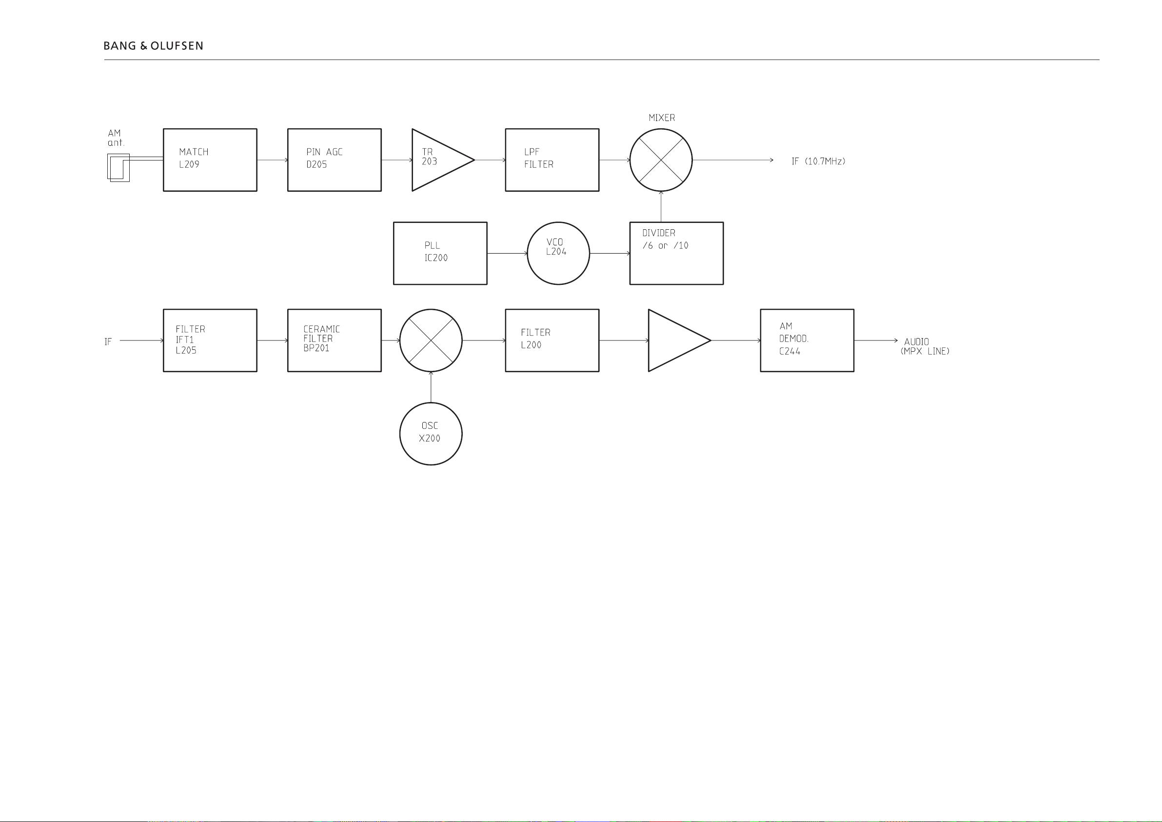
Block diagram for frontend tuner
2.5 Block diagramBlock diagram 2.5
Page 13
AM block diagram
2.6 Block diagramBlock diagram 2.6
2.6
Page 14
2.7
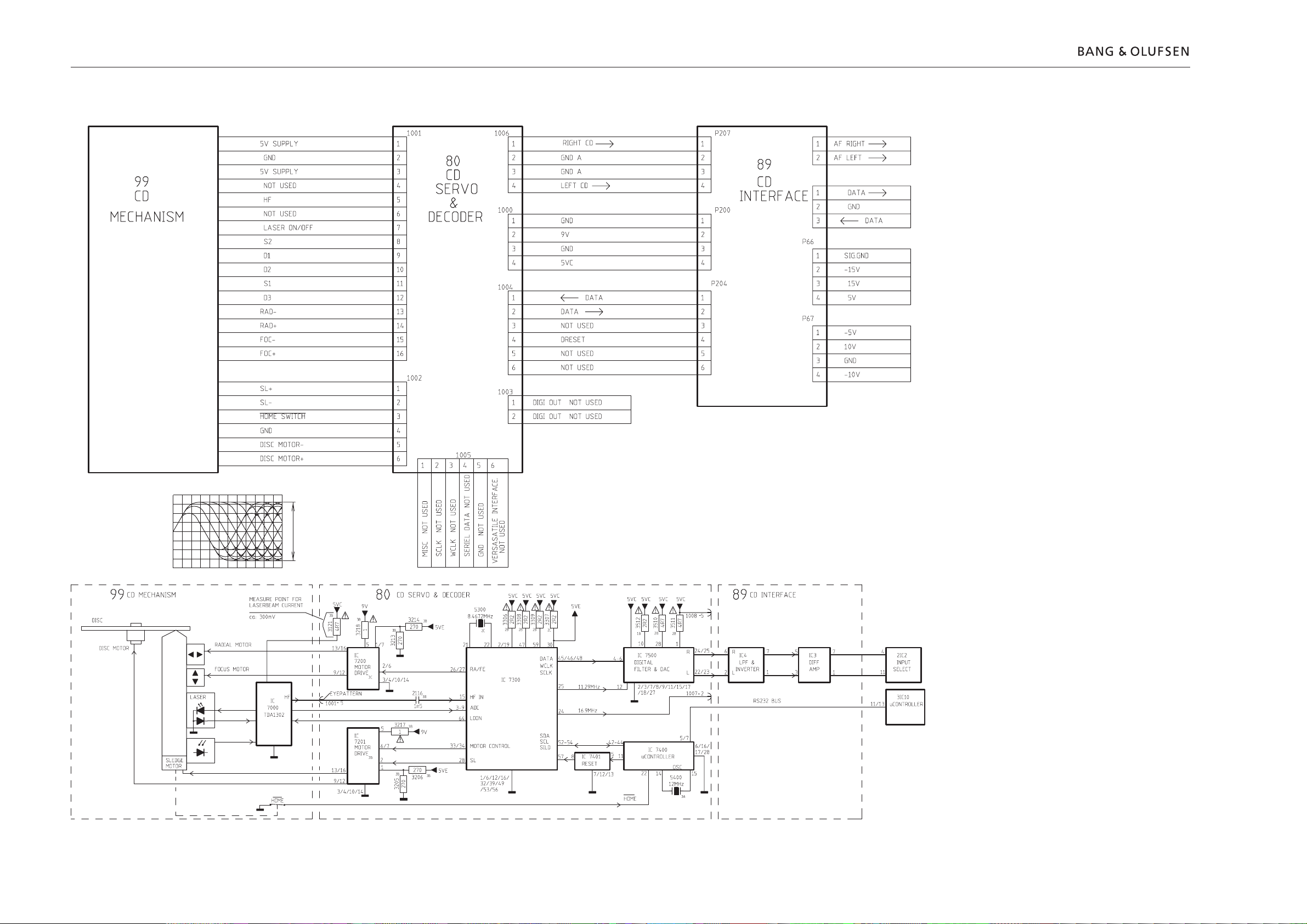
Block diagram for CD PRO
2.7 Block diagramBlock diagram 2.7
EYEPATTERN
2.5V
0.5µs/DIV
1.3V
Page 15
Block diagram for system key controle
2.8 Block diagramBlock diagram 2.8 2.8
Page 16
2.9
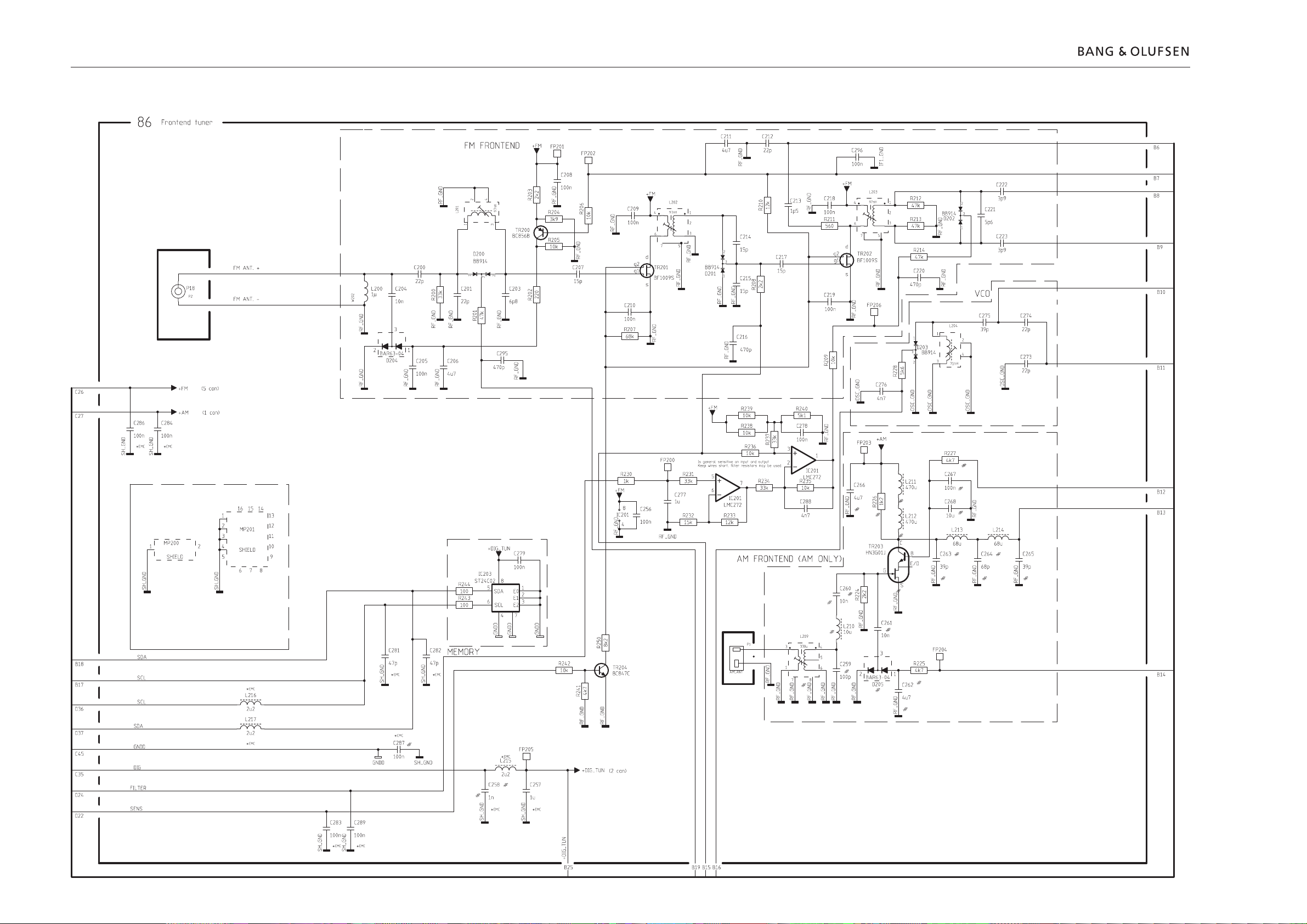
Diagram A – Frontend tuner PCB drawing for PCB86 see page 2.13
2.9 Diagram ADiagram A 2.9
Page 17
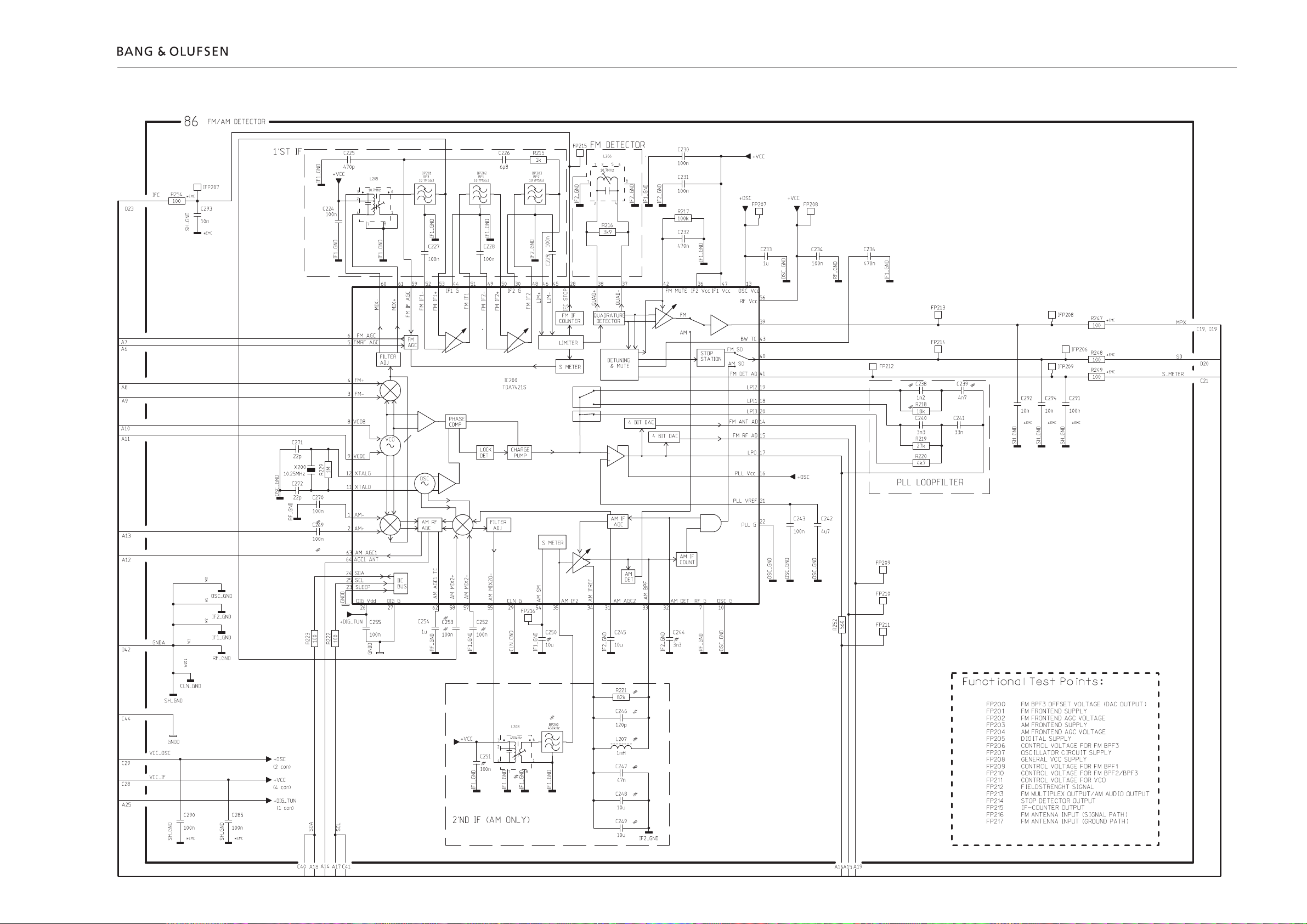
Diagram B – FM/AM Detector PCB drawing for PCB86 see page 2.13
2.10 Diagram BDiagram B 2.10
2.10
Page 18
2.11
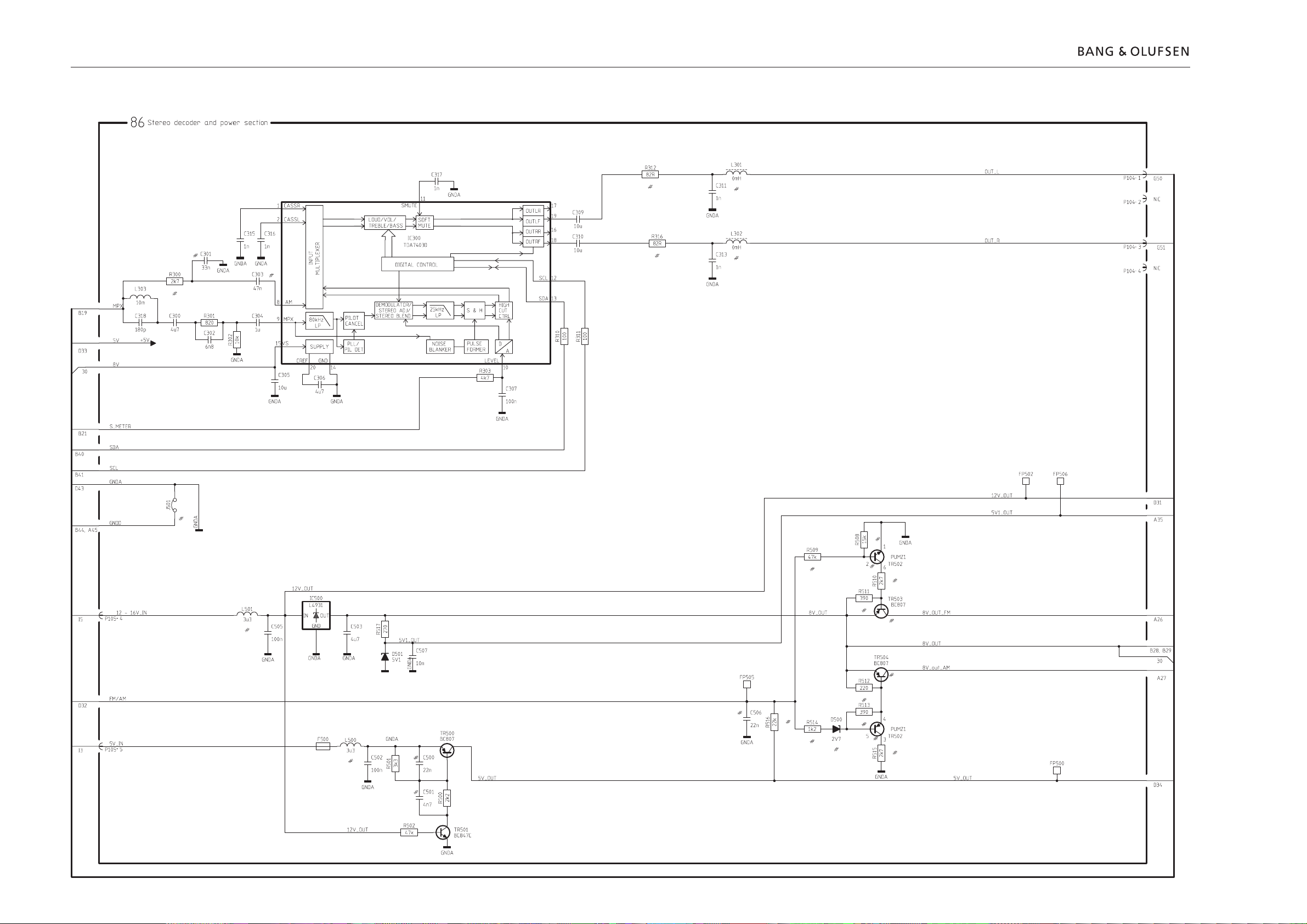
Diagram C – Stereo decoder and power section PCB drawing for PCB86 see page 2.13
2.11 Diagram CDiagram C 2.11
Page 19
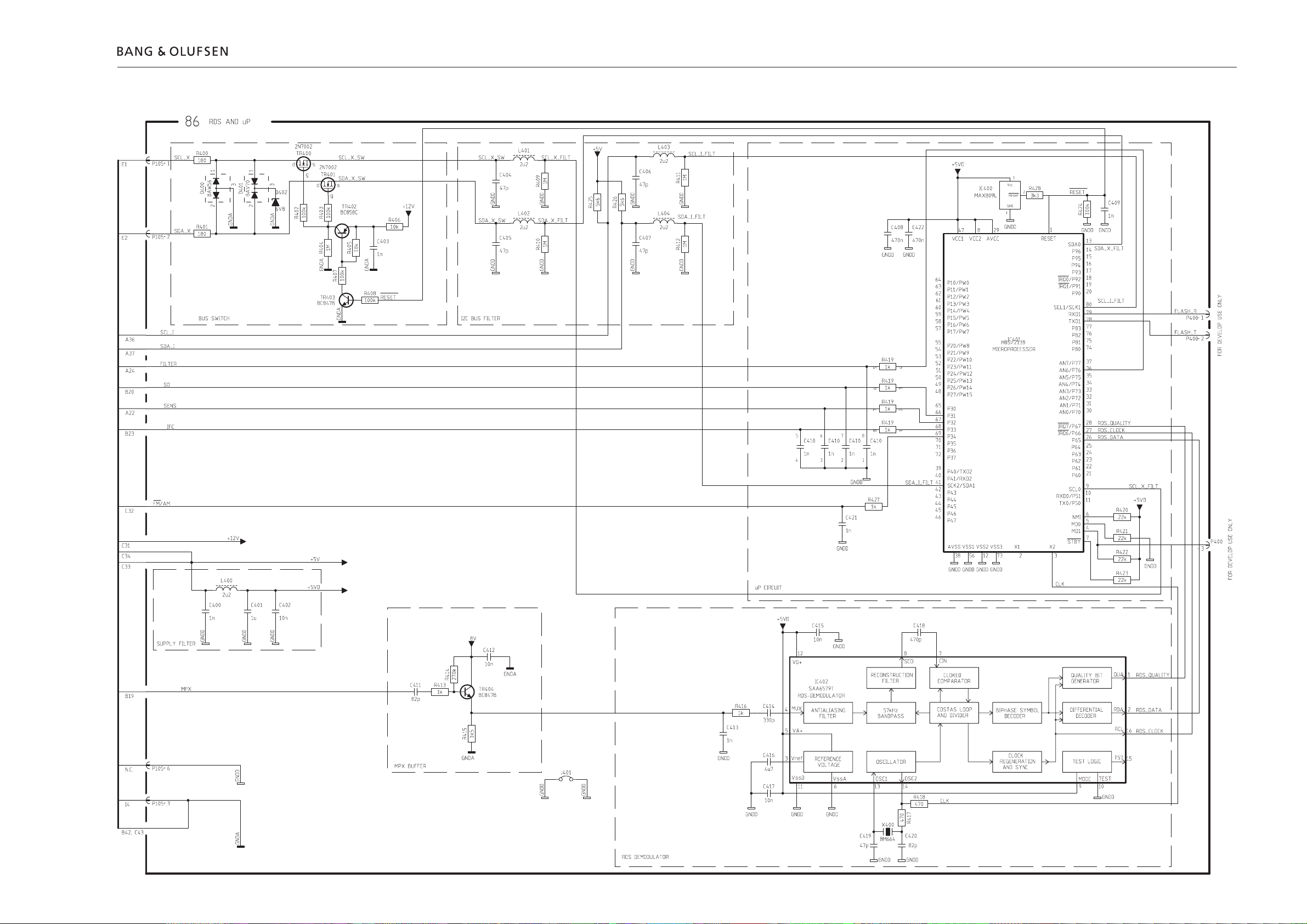
Diagram D – RDS, µP & IIC bus fi lter PCB drawing for PCB86 see page 2.13
2.12 Diagram DDiagram D 2.12
2.12
Page 20
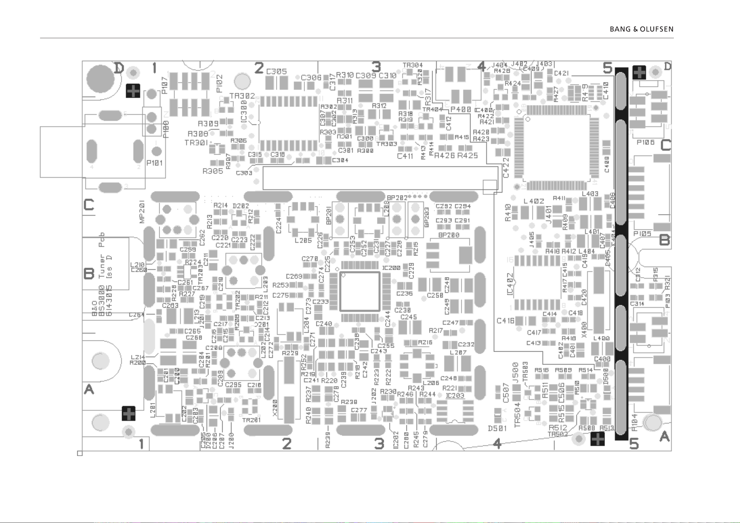
PCB86, Tuner-FM/AM-RDS-Stereo decoder
2.13 PCB drawingPCB drawing 2.132.13
Page 21
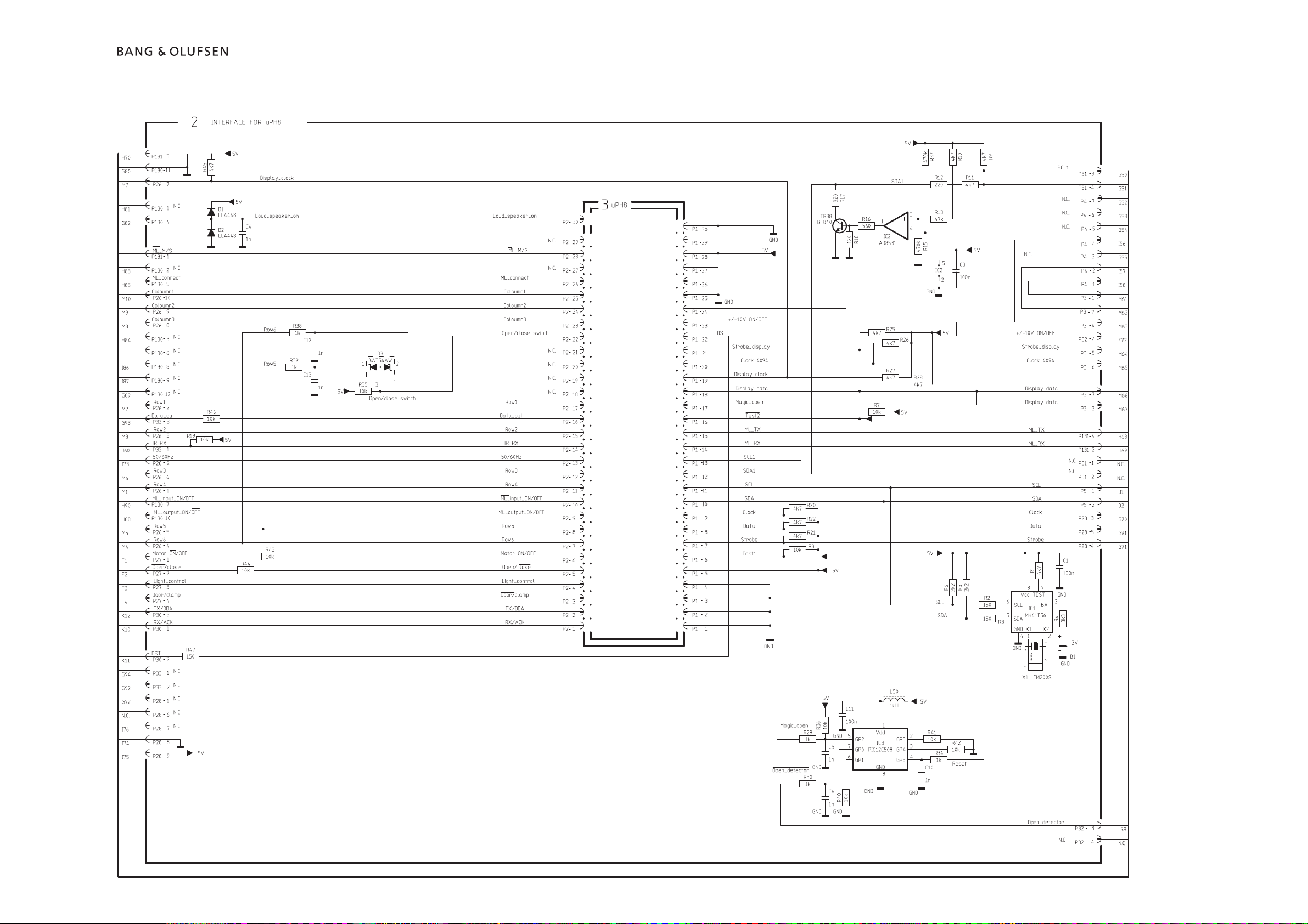
Diagram E – Interface for µP & µPH8 PCB drawing for PCB2 see page 2.16
2.14 Diagram EDiagram E 2.14
2.14
Page 22

2.15
Diagram F – Light and Motor control, Light supply & IR PCB drawing for PCB9 see page 2.16
2.15 Diagram FDiagram F 2.15
Page 23

PCB9, Light and motor control
PCB2, Interface f/µPH8
2.16 PCB drawingPCB drawing 2.16 2.16
Page 24

2.17
Diagram G – Input select PCB drawings for PCB12 see page 2.20
2.17 Diagram GDiagram G 2.17
Page 25

Diagram H – Master Link Interface PCB drawings for PCB12 see page 2.20
2.18 Diagram HDiagram H 2.18
2.18
Page 26

2.19
Diagram I – Power Supply & Transformer PCB drawings for PCB12 see page 2.20 PCB drawing for PCB15 see page 2.22
2.19 Diagram IDiagram I 2.19
Page 27

PCB12, Power Supply, Input select & Pre-amplifi er
2.20 PCB drawingsPCB drawings 2.20 2.20
Page 28

2.21
Diagram J – Door sensor PCB drawings for PCB20 & PCB21 see page 2.22
2.21 Diagram JDiagram J 2.21
Page 29

PCB20, IR receiver and left door sensor
2.22 PCB drawingsPCB drawings 2.22 2.22
PCB21, Door sensor right MKII
PCB15, Transformer
Page 30

2.23
2.23 Diagram KDiagram K 2.23
Diagram K – CD Interface
PCB5, Display
Page 31

Diagram L – CD Servo & Decoder
EYEPATTERN
2.24 Diagram LDiagram L 2.24
2.24
2.5V
0.5µs/DIV
1.3V
Page 32

2.25
Diagram M – Display & Keyboard PCB drawing for PCB5 see page 2.23
2.25 Diagram MDiagram M 2.25
Page 33

List of electrical parts
List of electrical parts 3.1
Resistors not referred to are standard, see page 3-9
PCB2, 8006796 Interface f/µPH8
PCB3, 8006797 µPH8 Microcomputer
IC1∆ 8342397 149 Memory/clock
M141T56M6
TR38* 8320740 51 BF 840
D1- 8300606 250 LL 4448
D2
D3 8301120 69 BAT 54AW
C1 4011135 100nF -20+80% 16V
C3 4010274 100nF -20+80% 25V
C4- 4010237 1nF 10% 50V
C6
L50 8021301 Coil 1µH 20%
X1 8090230 Crystal 32.768KHz
B1 8700027 Battery lithium 3V
P1- 7221357 Socket 30 pole
P2
P3- 7221378 Socket 7 pole
P4
P5 7221272 Plug 2 pole
P26 7221359 Plug 10 pole
P27 7221329 Plug 4 pole
IC2∆ 8343699 169 AD 8531
IC3∆ 8343682 151 PIC 12C508
C10 4010237 1nF 10% 50V
C11 4010316 100nF 10% 25V
C12- 4010237 1nF 10% 50V
C13
P28 7221356 Plug 9 pole
P30 7221330 Plug 3 pole
P31- 7221329 Plug 4 pole
P32
P33 7221330 Plug 3 pole
P130 7221361 Plug 12 pole
P131 7221329 Plug 4 pole
PCB5, 8001362 Display
∆ indicates that static electricity may destroy
the component
* specially selected or adapted sample
IC1∆ 8341025 150 4094B
IC2∆ 8343771 147 SN74ALS156
IC3∆ 8341079 151 µPD 7228
TR1- 8320755 51 BC 847B
TR6
TR8 8320755 51 BC 847B
TR13- 8320753 51 BC 856B
TR16
D1- 8300482 250 LL 4148
D2
DP1 8330259 Display, lower
DP2 8330468 Display, upper
R14- 5011912 1.2KΩ 1% 1/8W
R15
R18- 5011912 1.2KΩ 1% 1/8W
R19
R29 5011914 5.1KΩ 1% 1/8W
IC4∆ 8341226 150 4001B gate 4x2
input
TR17- 8320936 51 BC 847C
TR20
TR24 8320811 51 BC 857B
TR25 8320955 57 PMBF 4393
TR26 8320811 51 BC 857B
D3 8300577 250 Z3.9V 2% 0.5W
D4 8300661 250 Z4.3V 2% 0.5W
R39 5210006 LDR 3.3KΩ 33%
R40 5011912 1.2KΩ 1% 1/8W
R49 5012069 2KΩ 1% 1/8W
R56 5370435 1KΩ
R78 5370400 10KΩ
Page 34

3.2 List of electrical parts
Resistors not referred to are standard, see page 3-9
PCB9, 8001550 Light and motor control
C1- 4010166 100nF -20+80% 50V
C2
C4- 4010166 100nF -20+80% 50V
C5
C6 4000241 100pF 5% 50V
C8 4000241 100pF 5% 50V
X1 8030221 Crystal 455KHz
P41 7220714 Plug 7 pole
P42 7220717 Plug 10 pole
P43 7220710 Plug 3 pole
IC1∆- 8341420 136 TCA0372
IC2∆
TR1- 8320755 51 BC 847B
TR2
TR3- 8320811 51 BC 857B
TR7
TR8- 8320755 51 BC 847B
TR11
TR13 8320755 51 BC 847B
D1- 8300482 250 LL 4148
D2
D4 8300774 250 Z5.1V 5% 0.5W
D5- 8300482 250 LL 4148
D8
D9 8300723 250 Z8.2V 2% 0.5W
C9- 4010170 2.2nF 10% 50V
C12
C13- 4000241 100pF 5% 50V
C19
C20 4010157 10nF 10% 50V
C21 4200517 2.2µF 20% 50V
P44 7210853 Socket 13 pole
P45 7220710 Plug 3 pole
P46 7220724 Plug 2 pole
IC3∆ 8341041 138 LM 324
TR14 8320425 32 BD 436
TR21 8320507 18 BC 337-25
TR22 8320497 18 BC 547B
TR23 8320811 51 BC 857B
TR24 8320755 51 BC 847B
TR25 8320811 51 BC 857B
TR30 8320811 51 BC 857B
D10 8300577 250 Z3.9V 2% 0.5W
D14 8300772 250 Z24V 5% 0.4W
D16- 8300482 250 LL 4148
D19
D24 8300482 250 LL 4148
∆ indicates that static electricity may destroy
the component
R27 5010064 2.2KΩ 5% 1/4W
R28 5010069 3.9KΩ 5% 1/4W
R29 5010700 3.9KΩ 5% 1/2W
R31 5011378 0.82Ω 5% 1/4W
R32 5011845 8.2Ω1% 1/4W
R33 5011834 845Ω 1% 1/8W
R35 5011845 8.2Ω 1% 1/4W
R37 5011834 845Ω 1% 1/8W
R38 5011527 12KΩ 1% 1/8W
R39 5011752 12.7KΩ 1% 1/8W
R40 5011527 12KΩ 1% 1/8W
R41 5011752 12.7KΩ 1% 1/8W
R42 5021151 1.5Ω 1% 1/4W
R43 5011834 845Ω 1% 1/8W
R45 5021151 1.5Ω 1% 1/4W
C1 4010220 100nF 10% 50V
C3 4010220 100nF 10% 50V
C4 4200524 10µF 20% 25V
C5- 4000287 220nF -20+80% 25V
C6
C7 4200515 4.7µF 20% 25V
C11 4010157 10nF 10%
R47 5011854 2.1KΩ 1% 1/4W
R48 5011598 24.9KΩ 1% 1/8W
R49 5011838 18KΩ 1% 1/8W
R50 5011760 23.7KΩ 1% 1/8W
R67 5011601 200KΩ 1% 1/8W
R68 5011600 100KΩ 1% 1/8W
R69- 5011601 200KΩ 1% 1/8W
R71
R74- 5011595 26.7KΩ 1% 1/8W
R75
R78 5011600 100KΩ 1% 1/8W
R82- 5011598 24.9KΩ 1% 1/8W
R83
R101 5011600 100KΩ 1% 1/8W
C12 4010166 100nF -20+80% 50V
C13 4200524 10µF 20% 25V
C14- 4010157 10nF 10%
C16
Page 35

List of electrical parts 3.3
PCB12, 8001833 Power Supply, Input
select & Pre-amplifi er
P76 7220714 Plug 7 pole
P77 7220711 Plug 4 pole
P78- 7220709 Plug 2 pole
P80
IC1∆ 8341025 151 4094B
IC2∆ 8341059 151 4052
IC3∆ 8341025 151 4094B
IC4∆ 8342238 151 TDA 7318D
IC5∆ 8341225 151 LM 3578
TR1 8320427 32 BD 437
TR2- 8320428 32 BD 438
TR4
TR5 8320443 32 BD 442
TR6- 8320755 51 BC 847B
TR7
TR8- 8320512 18 BC 337-25
TR9
TR10- 8320523 17 BC 327-25
TR12
TR13 8320753 51 BC 856
TR14 8320755 51 BC 847B
TR15- 8320811 51 BC 857B
TR16
TR17- 8320755 51 BC 847B
TR19
TR20- 8320816 51 BC 846B
TR21
TR22 8320811 51 BC 857B
TR23 8320755 51 BC 847B
TR24 8320753 51 BC 856B
TR25- 8320755 51 BC 847B
TR33
P81 7220710 Plug 3 pole
IC6∆ 8341231 151 LF 347
IC7∆ 8341022 151 4558
IC8∆ 8340205 151 LF 347-TL074
IC10∆ 8341022 151 4558
IC11∆ 8341747 151 TL 7705BCD
TR34 8320936 51 BC 847C
TR35- 8320755 51 BC 847B
TR41
TR42- 8320811 51 BC 857B
TR45
TR46- 8320755 51 BC 847B
TR47
TR48- 8320759 51 BC 817-25B
TR49
TR50- 8320811 51 BC 857B
TR53
TR54- 8320856 54 2N7002
TR55
TR56 8320899 54 BSS 84P-50V
TR57- 8320811 51 BC 857B
TR59
TR60- 8321080 51 FMMT 491ATA
TR63
TR64 8320811 51 BC 857B
TR65 8320941 51 2SC 4213
TR66 8320753 51 BC 856B
TR67 8320755 51 BC 847B
TR68 8320941 51 2SC 4213
D1- 8300907 250 GF 1B
D2
D3- 8300520 250 Z6.8V 5% 0.5W
D6
D7- 8300562 250 Z5.6V 2% 0.5W
D8
D9- 8300605 250 Z10.0V 5% 0.5W
D10
D11- 8300606 250 LL 4448
D23
D24 8300562 250 Z5.6V 2% 0.5W
D25- 8300606 250 LL 4448
D34
D35 8301045 250 BAS 216
D36 8300607 250 Z3.3V 5% 0.4W
D37- 8300606 250 LL 4448
D40
R4 5011557 10KΩ 1% 1/8W
R8 5011332 10MΩ 10% 1/8W
R9 5011557 10KΩ 1% 1/8W
R10 5011792 4.75KΩ 1% 1/8W
R11- 5011599 49.9KΩ 1% 1/8W
R12
R13- 5011632 1.5KΩ 1% 1/4W
R16
R17- 5011912 1.2KΩ 1% 1/8W
R18
R19- 5011914 5.1KΩ 1% 1/8W
R21
D41 8300914 250 SS 14
D42- 8300644 250 Z6.2V 2% 0.5W
D43
D44 8300645 250 Z3.3V 2% 0.5W
D45 8300677 250 Z4.7V 5% 0.5W
D46- 8300723 250 Z8.2V 2% 0.5W
D47
D48- 8300726 250 Z7.5V 2% 0.5W
D49
D50 8300762 250 Z9.1V 2% 0.5W
D51 8300914 250 SS 14
D52 8300482 250 LL 4148
D55- 8300606 250 LL 4448
D56
R74 5011903 180Ω 1% 1/4W
R263 5011982 698Ω 1% 1/8W
R264 5011871 365Ω 1% 1/8W
R265 5011984 5.62KΩ 1% 1/8W
R266 5011987 28.7KΩ 1% 1/8W
R267 5011988 22KΩ 1% 1/8W
R268 5012057 6.8KΩ 1% 1/8W
R269 5012317 46.4KΩ 1% 1/10W
R271- 5012331 10KΩ 1% 1/10W
R272
R273 5012350 27.4KΩ 1% 1/10W
R274 5021542 0.22Ω 5% 1/4W
∆ indicates that static electricity may destroy
the component
C1- 4000233 220pF 5% 50V
C4
C5 4000277 22pF 5% 50V
C6 4000351 1.5nF 5% 50V
C7 4000412 100pF 5% 50V
C8 4000381 820pF 5% 50V
C9- 4000408 47pF 5% 50V
C14
C15- 4000412 100pF 5% 50V
C16
Page 36

3.4 List of electrical parts
Resistors not referred to are standard, see page 3-9
C17 4000418 330pF 5% 50V
C18- 4000416 220pF 5% 50V
C24
C25 4000418 330pF 5% 50V
C26 4000420 470pF 5% 50V
C27- 4000457 1.5nF 5% 50V
C28
C29 4000420 470pF 5% 50V
C30- 4000461 1nF 5% 50V
C33
C34 4010132 1nF 10% 50V
C35 4010209 47nF 10% 50V
C36 4000461 1nF 5% 50V
C37 4010132 1nF 10% 50V
C38 4010176 10nF -20+80% 50V
C39 4010237 1nF 10% 50V
C40- 4010262 1.8nF 10% 50V
C41
C42- 4010269 6.8nF 10% 50V
C43
C44- 4010271 10nF 10% 50V
C45
C48- 4010237 1nF 10% 50V
C50
C51 4010263 2.2nF 10% 50V
C52- 4010271 10nF 10% 50V
C56
C59- 4010271 10nF 10% 50V
C65
C66- 4010274 100nF -20+80% 25V
C67
C68 4010334 220nF 10% 16V
C69 4010271 10nF 10% 50V
C70- 4010316 100nF 10% 25V
C71
C72 4010316 100nF 10% 25V
C73- 4130307 150nF 10% 63V
C76
C77 4201256 470µF 20% 25V
C78 4010271 10nF 10% 50V
C79 4200824 22µF 20% 50V
C80- 4010271 10nF 10% 50V
C81
C82- 4010272 22nF -20+80% 50V
C84
C85 4010274 100nF -20+80% 25V
C86 4010314 220nF -20+80% 25V
C87- 4201174 2.2µF 20% 50V
C88
C89 4201301 220µF -20+50% 16V
C90 4200824 22µF 20% 50V
C91- 4201173 10µF 20% 50V
C95
C96 4200824 22µF 20% 50V
C97 4201537 1000µF 20% 35V
C98- 4201173 10µF 20% 50V
C99
C100- 4201173 10µF 20% 50V
C106
C107 4201474 330µF 20% 63V
C108- 4201171 1µF 20% 50V
C109
C110 4201173 10µF 20% 50V
C111- 4201170 0.47µF 20% 50V
C112
C113- 4201173 10µF 20% 50V
C121
C122- 4201174 2.2µF 20% 50V
C123
C124 4000287 220nF -20+80% 25V
C125 4010272 22nF -20+80% 50V
C126- 4010274 100nF -20+80% 25V
C127
C128 4200961 220µF 20% 10V
C129- 4010237 1nF 10% 50V
C133
C134 4000290 22nF 10% 50V
L1 8021274 Coil 330µH 10%
L2- 8020821 Coil 2.2µH 5%
L3
F1 6604038 Fuse 1AF 250V
P1 7210418 Socket 7 pole DIN
P2- 7210689 Socket 8 pole DIN
P3
P4 7210904 Socket 16 pole
ML-socket
P11- 7220711 Plug 4 pole
P13
P14- 7220709 Plug 2 pole
P15
P16 7220712 Plug 5 pole
P17 7220714 Plug 7 pole
P18 7220710 Plug 3 pole
L4- 8021003 Coil 100µH 5%
L7
P19 7220712 Plug 5 pole
P20 7220716 Plug 9 pole
P21 7220709 Plug 2 pole
P22 7220711 Plug 4 pole
P23 7220710 Plug 3 pole
P25 7220711 Plug 4 pole
P100 7211195 Socket 10 pole
P103- 7220711 Plug 4 pole
P104
P105 7211186 Socket 8 pole
P107 7220711 Plug 4 pole
P108 7220719 Plug 12 pole
Page 37

List of electrical parts 3.5
PCB14, 8001771 Master Link Audio interface
PCB15, 8001834 Transformer EU
IC1∆- 8341022 138 4558
IC7∆
TR3 8320811 51 BC 857B
TR4- 8320755 51 BC 847B
TR5
R2 5011841 11.8KΩ 1% 1/8W
R4 5011841 11.8KΩ 1% 1/8W
R5- 5011531 5.9KΩ 1% 1/8W
R6
R8 5011841 11.8KΩ 1% 1/8W
R10 5011841 11.8KΩ 1% 1/8W
R11- 5011531 5.9KΩ 1% 1/8W
R12
C1- 4000277 22pF 5% 50V
C2
C3- 4000241 100pF 5% 50V
C4
C6- 4000241 100pF 5% 50V
C7
TR1 8320427 32 BD 437
TR2- 8320428 32 BD 438
TR4
D1- 8300023 209 1N 4002
D4
IC8- 8341024 150 4066
IC10
TR6 8320811 51 BC 857B
R14- 5011557 10KΩ 1% 1/8W
R15
R19- 5011557 10KΩ 1% 1/8W
R20
R23- 5011571 75Ω 1% 1/8W
R26
C11- 4010166 100nF -20+80% 50V
C14
C100- 4000345 1nF 5% 50V
C101
D5- 8300907 250 DO-214BA
D14
PCB15, 8006798 Transformer US
R10 5020625 2.7Ω 5% 0.3W
C1- 4010166 100nF -20+80% 50V
C6
C7- 4010216 22nF 10% 100V
C9
C10 4201111 6800µF 20% 16V
C11 4201426 3300µF 20% 16V
L1 8022295 Coil 2 x 0.4mH
T1 8013501 Mains transformer 100V-120V-230V-240V
F1- 6600155 Fuse 1.6 AT 250V
F4
F5 6600067 Fuse 2.5 AT 250V
P24 7220715 Plug 8 pole
7219087 Mains socket
R1 5000194 3.3Mohm 10% 1/2W
F1- 6600162 Fuse 1.6 AT 125V
F4
F5 6600081 Fuse 2.5 AT 125V
All other electrical parts see PCB15, Transformer EU
C12 4201425 6800µF 20% 16V
C13 4200821 1000µF -20+50% 6.3V
C14- 4201098 4700µF 20% 35V
C15
C16- 4010166 100nF -20+80% 50V
C19
PCB18, 8001817 Headphone
∆ indicates that static electricity may destroy
the component
Page 38

3.6 List of electrical parts
Resistors not referred to are standard, see page 3-9
PCB20, 8005738 IR receiver and left door sensor
IC1∆ 8341041 138 LM 324
TR1- 8320740 51 BF 840
TR2
TR3- 8320755 51 BC 847B
TR7
TR12- 8320755 51 BC 847B
TR16
D1 8300482 250 LL 4148
D3- 8300482 250 LL 4148
D6
R20 5011985 13.3KΩ 1% 1/8W
R28- 5012258 215KΩ 1% 1/8W
R30
R31 5012331 10KΩ 1% 1/10W
R53- 5012164 1MΩ 1% 1/8W
R56
R57 5012240 100KΩ 1% 1/10W
C1 4010257 15nF 10% 50V
C2- 4000408 47pF 5% 50V
C5
C6- 4000414 150pF 5% 50V
C13
C14- 4000420 470pF 5% 50V
C19
C20- 4010263 2.2nF 10% 50V
C21
C22- 4010271 10nF 10% 50V
C23
L1 8020562 Coil 455KHz
TR17 8320769 51 BC 849C
TR18- 8320811 51 BC 857B
TR21
TR22 8321072 19 ZTX 690B
TR23 8321073 19 ZTX 790A
D7- 8330145 244 Ir detector
D8
R66 5012467 13.3Ω 1% 1/10W
R67 5012466 22.1Ω 1% 1/10W
R68- 5020981 1.8Ω 10% 0.35W
R69
R70 5021047 10Ω 5% 0.14W
R71- 5012365 11KΩ 1% 1/10W
R73
C24 4010314 220nF -20+80% 25V
C25 4010195 2.7nF 5% 50V
C26- 4010316 100nF 10% 25V
C29
C30 4130313 470nF 20% 63V
C32 4200510 10µF 20% 16V
C33 4010316 100nF 10% 25V
C34 4200510 10µF 20% 16V
C35 4010316 100nF 10% 25V
C217 4200510 10µF 20% 16V
C219 4200961 220µF 20% 10V
PCB21, 8006799 Door sensor right
symbol of safety components, see page 2.1
∆ indicates that static electricity may destroy
the component
BP1 8030056 Cer. fi lter 455KHz
P46 7220726 Plug 4 pole
P47 7220725 Plug 3 pole
P49 7220725 Plug 3 pole
P50 7220728 Plug 6 pole
IC1∆ 8341041 138 LM 324
TR3 8320755 51 BC 847B
TR7 8320755 51 BC 847B
TR32 8320755 51 BC 847B
R2 5011632 1.5KΩ 1% 1/4W
R5 5012240 100KΩ 1% 1/10W
R6 5012331 10KΩ 1% 1/10W
R10 5012164 1MΩ 1% 1/8W
R12 5012258 215KΩ 1% 1/8W
R15 5012164 1MΩ 1% 1/8W
R17 5012258 215KΩ 1% 1/8W
R20 5012164 1MΩ 1% 1/8W
P83 7220693 Contact pin 2 pole
P132 7220730 Plug 8 pole
P133 7220729 Plug 7 pole
P250 7220727 Plug 5 pole
TR36- 8320755 51 BC 847B
TR37
TR47 8320811 51 BC 847B
R22 5012258 215KΩ 1% 1/8W
R25 5012164 1MΩ 1% 1/8W
R38 5012466 22.1Ω 1% 1/10W
R39 5012467 13.3Ω 1% 1/10W
R53 5021047 10Ω 5% 0.14W
R65- 5012365 11KΩ 1% 1/10W
R67
Page 39

List of electrical parts 3.7
PCB28, 3358279 Light supply
PCB86, 8006800 Tuner-FM/AM-RDSStereo decoder EU/US
C2 4010316 100nF 10% 25V
C4 4010263 2.2nF 10% 50V
C8- 4000414 150pF 5% 50V
C9
C13- 4000414 150pF 5% 50V
C14
C18 4000414 150pF 5% 50V
C19 4000229 150pF 5% 50V
C23- 4000414 150pF 5% 50V
C24
P1 7220710 Plug 3 pole
P2 7220728 Plug 6 pole
P3 7220727 Plug 5 pole
TR1 8320425 32 BD 436
D1- 8300557 250 BYM10
D4
C1- 4000345 1nF 5% 50V
C3
IC200∆ 8343626 147 TDA 7421S
IC201∆ 8343652 151 LMC 272
IC203∆ 8342519 151 EEPROM
M24C02-MN6T
Advanced adjustments procedure when
replacing this component. Replacement of
PCB86 is recommended 8006800.
C27 4010157 10nF 10% 50V
C30 4010271 10nF 10% 50V
C33 4200826 10µF 20% 16V
C49 4010195 2.7nF 5% 50V
C52 4200961 220µF 20% 10V
C57- 4010316 100nF 10% 25V
C58
C59 4200510 10µF 20% 16V
C60 4010316 100nF 10% 25V
IC300∆ 8343681 136 TDA 7403
IC400∆ 8343809 170 MAX 809L
IC401∆ 8343673 147 µP H8S/2138
IC402∆ 8342568 136 SAA 6579T
IC500∆ 8343733 168 L 4931
TR200 8320753 51 BC 856B
TR201- 8321276 53 Mosfet 9V 1GHz
TR202
TR203 8321277 169 HN 3G01J
TR204 8320936 51 BC 847C
TR301 8321198 136 PUM X1
TR302 8320778 51 BC 857
TR303- 8321080 51 FMMT 491ATA
TR304
TR400- 8320856 68 2N 7002
TR401
D200- 8301140 252 BB 914
D203
D204- 8301143 267 BAR 63-04
D205
D400 8300894 69 BAW 56
R208 5013156 2.2KΩ 1% 1/16W
R209 5012331 10KΩ 1% 1/10W
R216 5013244 3.9KΩ 1% 1/16W
R226 5013152 1.2KΩ 5% 1/16W
R231 5012238 33KΩ 1% 1/10W
R234 5012238 33KΩ 1% 1/10W
R235- 5012331 10KΩ 1% 1/10W
R236
R237 5012238 33KΩ 1% 1/10W
R238- 5012331 10KΩ 1% 1/10W
R239
R240 5012559 5.1KΩ 1% 1/10W
TR402 8320778 51 BC 857
TR403- 8320755 51 BC 847B
TR404
TR500 8320971 51 BC 807-40
TR501 8320936 51 BC 847C
TR502 8321196 136 PUM Z1
TR503- 8320971 51 BC 807-40
TR504
D401 8300895 252 BAV 70
D402 8300520 250 Z6.8V 5% 0.5W
D500 8301056 250 Z2.7V 2% 0.4W
D501 8301064 250 Z5.1V 2% 0.4W
R300 5013242 2.7KΩ 1% 1/16W
R301 5013236 820Ω 1% 1/16W
R400- 5011903 180Ω 1% 1/4W
R401
R415 5013239 1.5KΩ 1% 1/16W
R419 5030051 4 x 1KΩ 5% 1/16W
R425- 5013246 5.6KΩ 1% 1/16W
R426
R428 5013243 3.3KΩ 1% 1/16W
R514 5013238 1.2KΩ 1% 1/16W
R517 5021532 270Ω 1% 1/4W
∆ indicates that static electricity may destroy
the component
C200 4000404 22pF 5% 50V
C201 4001127 22pF 5% 50V
C203 4001121 6.8pF 50V
C204 4011122 10nF 10% 50V
C205 4011134 100nF 10% 16V
C206 4010419 4.7µF 10% 10V
C207 4001125 15pF 5% 50V
C208 4011134 100nF 10% 16V
C209- 4011135 100nF -20+80% 16V
C210
C211 4010434 4.7µF
C212 4000404 22pF 5% 50V
C213 4001118 3.9pF 5% 50V
C214- 4001125 15pF 5% 50V
C215
C216 4001143 470pF 5% 50V
Page 40

3.8 List of electrical parts
Resistors not referred to are standard, see page 3-9
C217 4001125 15pF 5% 50V
C218- 4011135 100nF -20+80% 16V
C219
C220 4001143 470pF 5% 50V
C221 4001120 5.6pF 5% 50V
C222- 4001118 3.9pF 5% 50V
C223
C224 4011135 100nF -20+80% 16V
C225 4001143 470pF 5% 50V
C226 4001121 6.8pF 50V
C227- 4011134 100nF 10% 16V
C231
C232 4010387 470nF 10% 16V
C233 4010323 1µF -20+80% 16V
C234 4010274 100nF -20+80% 25V
C236 4010387 470nF 10% 16V
C238 4000493 1.2nF 10% 50V
C239 4000494 4.7nF 10% 50V
C240 4000495 3.3nF 10% 50V
C241 4000496 33nF 10% 50V
C242 4010419 4.7µF 10% 10V
C243 4011134 100nF 10% 16V
C244 4000495 3.3nF 10% 50V
C245 4010420 10µF 10% 10V
C246 4001136 120pF 5% 50V
C247 4011130 47nF 10% 16V
C248- 4010420 10µF 10% 10V
C250
C251 4010316 100nF 10% 25V
C252- 4011134 100nF 10% 16V
C253
C254 4010421 1µF 10% 16V
C255 4011134 100nF 10% 16V
C256 4010316 100nF 10% 25V
C257 4010323 1µF -20+80% 16V
C258 4010237 1nF 10% 50V
C259 4001135 100pF 5% 50V
C260- 4011122 10nF 10% 50V
C261
C262 4010419 4.7µF 10% 10V
C263 4001130 39pF 5% 50V
C264 4001133 68pF 5% 50V
C265 4001130 39pF 5% 50V
C266 4010322 4.7µF -20+80% 16V
C267 4011134 100nF 10% 16V
C268 4010420 10µF 10% 10V
C269- 4011134 100nF 10% 16V
C270
C271- 4001127 22pF 5% 50V
C274
C275 4001130 39pF 5% 50V
C276 4000494 4.7nF 10% 50V
C277 4010421 1µF 10% 16V
C278 4010316 100nF 10% 25V
C279 4011134 100nF 10% 16V
C281- 4000408 47pF 5% 50V
C282
C283- 4010274 100nF -20+80% 25V
C287
C288 4000494 4.7nF 10% 50V
C289- 4010274 100nF -20+80% 25V
C290
C291 4011134 100nF 10% 16V
C292- 4011122 10nF 10% 50V
C294
C295 4001143 470pF 5% 50V
C296 4011135 100nF -20+80% 16V
C300 4010419 4.7µF 10% 10V
C301 4011128 33nF 10% 25V
C302 4011120 6.8nF 10% 50V
C303 4011130 47nF 10% 16V
C304 4010421 1µF 10% 16V
C305 4010435 10µF -20+80% 25V
C306 4010419 4.7µF 10% 10V
C307 4011134 100nF 10% 16V
C309- 4010420 10µF 10% 10V
C310
C311 4010237 1nF 10% 16V
C313 4010237 1nF 10% 16V
C315- 4011110 1nF 10% 50V
C317
C318 4001138 180pF 5% 50V
C400 4011110 1nF 10% 50V
C401 4010321 470nF -20+80% 16V
C402 4011122 10nF 10% 50V
C403 4010237 1nF 10% 16V
C404- 4001131 47pF 5% 50V
C407
C408 4010321 470nF -20+80% 16V
C409 4011110 1nF 10% 50V
C410 4011056 4 x 1nF 10% 50V
C411 4001134 82pF 5% 50V
C412 4011122 10nF 10% 50V
C413 4011110 1nF 10% 50V
C414 4001141 330pF 5% 50V
C415 4011122 10nF 10% 50V
C416 4010419 4.7µF 10% 10V
C417 4011122 10nF 10% 50V
C418 4001143 470pF 5% 50V
C419 4001131 47pF 5% 50V
C420 4001134 82pF 5% 50V
C421 4011110 1nF 10% 50V
C422 4010321 470nF -20+80% 16V
C500 4010315 22nF 10% 25V
C501 4010267 4.7nF 10% 50V
C502 4010316 100nF 10% 25V
C503 4010434 4.7µF
C505 4010316 100nF 10% 25V
C506 4010315 22nF 10% 25V
C507 4011122 10nF 10% 50V
L200 8021078 Coil 1µH 10%
L201 8021319 Coil 97nH
L202- 8021320 Transformer 97nH
L203
L204 8021318 Coil 71nH
L205 8021322 Transformer 10.7MHz
L206 8021321 Coil 10.7MHz
L207 8021325 Coil 1mH
L208 8021323 Transformer 450KHz
L209 8020909 Coil 330µH 10% 796KHz
L210 8021324 Coil 10µH
Page 41

3.9 List of electrical partsList of electrical parts 3.9 3.9
PCB86, 8006801 Tuner-FM/AM-RDSStereo decoder JAP
PCB89, 8001867 Interface f/CD PRO MKI
L211- 8020626 Coil 470µH 5%
L212
L213- 8020714 Coil 68µH 10%
L214
L215- 8020821 Coil 2.2µH 5%
L217
L301- 6000064 Jumper
L302
BP200 8030391 Cer. fi lter 450KHz ±KHz
BP201- 8030400 Cer. fi lter 10.7MHz
BP203
X200 8090274 Crystal 10.25MHz X400 8090206 Crystal 8.664MHz
F500 6604039 Fuse 200mA
P100 7210612 Socket antenna mini-jack
P101 7221373 Male connector
P102 7221082 Plug 2 pole
P103 7211221 Socket 4 pole
P104 7221131 Plug 4 pole
MP100 3302584 Shield f/FM-tuner
MP200 3320430 Shield radio
IC203∆ 8342519 151 EEPROM M24C02-MN6T
Advanced adjustments procedure when replacing this component.
Replacement of PCB86 is recommended 8006801.
C248- 4010420 10µF 10% 10V
C250
All other electrical parts see PCB86, Tuner EU/US
IC1 8340796 105 7805 2% 5V
IC2∆ 8341041 138 LM 324
TR2 8320755 51 BC 847B
TR3 8321050 19 ZTX 788-STZ
D3 8300201 250 Z6.2V 5% 0.4W
L303 8021345 Coil 10mH
L400- 8020821 Coil 2.2µH 5%
L404
L500- 8020822 Coil 3.3µH 5%
L501
P105 7221157 Plug 6/6 pole
P106 7211222 Socket 6 pole
P107 7221082 Plug 2 pole
P400 7211221 Socket 4 pole
MP201 3320431 Shield
IC3- 8341022 138 4558
IC4
TR4 8320755 51 BC 847B
TR5 8320811 51 BC 857B
Standard resistors
Resistors SMD 2% 1/8 W
SMD 5% 1/8 W
Glue dots, approx. 200, part no. 3181932
0.55mm
3.2mm
1.6mm
Resistors SMD 5% 1/10 W
Glue dots, approx. 200, part no. 3181932
0.55mm
2.0mm
1.25mm
5% 2% 2% 2% 2% 2% 5% 2%
x1 x10 x100 x1K x10K x100K x1M x10M
1.0 5011623 5011647 5011218 5011227 5011241 5011256 5011267 5011730
1.1 5011624 5011648 5011669 5011681 5011689 5011694 5011707
1.2 5011625 5011649 5011219 5011682 5011490 5011257 5011708
1.3 5011626 5011650 5011670 5011683 5011242 5011258 5011709
1.5 5011627 5011651 5011220 5011228 5011243 5011259 5011710
1.6 5011628 5011652 5011671 5011684 5011690 5011695 5011711
1.8 5011629 5011653 5011672 5011229 5011244 5011260 5011712
2.0 5011630 5011654 5011673 5011685 5011691 5011696 5011713
2.2 5011216 5011655 5011674 5011230 5011245 5011261 5011714
2.4 5011634 5011656 5011675 5011686 5011246 5011697 5011715
2.7 5011635 5011657 5011497 5011231 5011247 5011262 5011716
3.0 5011731 5011658 5011499 5011500 5011692 5011698 5011717
3.3 5011217 5011659 5011676 5011232 5011248 5011263 5011718
3.6 5011636 5011660 5011677 5011687 5011249 5011264 5011719
3.9 5011637 5011661 5011221 5011233 5011491 5011699 5011720
4.3 5011638 5011662 5011498 5011688 5011492 5011700 5011721
4.7 5011639 5011269 5011222 5011234 5011250 5011265 5011722
5.1 5011640 5011663 5011678 5011235 5011493 5011701 5011723
5.6 5011641 5011664 5011223 5011236 5011251 5011702 5011724
6.2 5011642 5011665 5011224 5011237 5011693 5011703 5011725
6.8 5011643 5011666 5011225 5011238 5011252 5011704 5011726
7.5 5011644 5011667 5011679 5011239 5011253 5011705 5011727
8.2 5011645 5011270 5011226 5011240 5011254 5011266 5011728
9.1 5011646 5011668 5011680 5011489 5011255 5011706 5011729
x1 x10 x100 x1K x10K x100K x1M x10M
0.0 6000072
1.0 5011920 5011932 5011944 5011956 5011968 5011980 5012275
1.2 5012326 5011921 5011933 5011945 5011957 5011969 5012267
1.5 5012379 5011922 5011934 5011946 5011958 5011970 5012268
1.8 5012380 5011923 5011935 5011947 5011959 5011971 5011989
2.2 5011924 5011936 5011948 5011960 5011972 5012220
2.7 5011925 5011937 5011949 5011961 5011973 5012269
3.3 5011926 5011938 5011950 5011962 5011974 5012261
3.9 5011927 5011939 5011951 5011963 5011975 5012270
4.7 5012472 5011928 5011940 5011952 5011964 5011976 5012271
5.6 5011929 5011941 5011953 5011965 5011977 5012272
6.8 5011930 5011942 5011954 5011966 5011978 5012273
8.2 5011931 5011943 5011955 5011967 5011979 5012274
∆ indicates that static electricity may destroy
the component
R27- 5011986 15.4KΩ 1% 1/8W
R28
R29- 5012290 4.87KΩ 1% 1/10W
R30
R31- 5012297 5.62KΩ 1% 1/10W
R32
C1- 4000351 1.5nF 5% 50V
C2
C3- 4000414 150pF 5% 50V
C4
C5- 4000416 220pF 5% 50V
C6
C11- 4010314 220nF -20+80% 25V
C13
C14- 4010272 22nF -20+80% 50V
C16
C17- 4010274 100nF -20+80% 25V
C19
P65 7220709 Plug 2 pole
P66- 7220711 Plug 4 pole
P67
P68 7220710 Plug 3 pole
R34- 5012331 10KΩ 1% 1/10W
R35
R36- 5011557 10KΩ 1% 1/8W
R39
R40- 5012331 10KΩ 1% 1/10W
R41
C20- 4201173 10µF 20% 50V
C21
C23- 4201174 2.2µF 20% 50V
C24
C25 4200524 10µF 20% 25V
C26 4010274 100nF -20+80% 25V
C30 4010272 22nF -20+80% 50V
C31 4010166 100nF -20+80% 50V
C37 4010314 220nF -20+80% 25V
C38 4010274 100nF -20+80% 25V
C39 4010271 10nF 10% 50V
P200 7220711 Plug 4 pole
P204 7220713 Plug 6 pole
P207 7220711 Plug 4 pole
Resistors SMD 5% 1/16 W
0.45mm
1.6mm
0.8mm
x1 x10 x100 x1K x10K x100K x1M x10M
1.0 5013201 5013213 5013225 5013237 5013249 5013261 5013273 5013285
1.2 5013202 5013214 5013226 5013262 5013274
1.5 5013203 5013215 5013227 5013263
1.8 5013204 5013216 5013228 5013240 5013276
2.2 5013205 5013217 5013229 5013241 5013253 5013265 5013277
2.7 5013206 5013218 5013254 5013266 5013278
3.3 5013207 5013231 5013040 5013255 5013267 5013279
3.9 5013208 5013220 5013268 5013280
4.7 5013209 5013221 5013233 5013245 5013257 5013269 5013281
5.6 5013210 5013222 5013234 5013258 5013270 5013282
6.8 5013211 5013223 5013235 5013259 5013271 5013283
8.2 5013212 5013224 5013135 5013260 5013272 5013284
Page 42

List of mechanical parts
Front
9001
9002
4.1 List of mechanical partsList of mechanical parts 4.14.1
9021
6
9022
9023
9024
6
9025
1
1
1
1
9
1
9008
9009
9003
9004
9005
9006
9007
9026
9027
2
2
2
2
9005
7
7
7
9011
0501
9012
9013
0502
0503
05DP2
0504
5
4
90/99
6
6
9024
9025
9024
9025
9027
4
5
9010
3
9014
0505
0501
9012
3
9013
0502
0503
05DP1
0504
3
9014
0506
9015
3
9016
3
9017
3
3
9018
87/89
9019
3
9028
9020
9029
Page 43

4.2 List of mechanical partsList of mechanical parts 4.2 4.2
Front
9001 3162622 Cover, left
9002 3162830 Glass, left
9003 2802056 Ring f/clamper with magnet strips
9004 3017028 Wheel
9005 2830111 Cylinder pin
9006 3162652 Clamper
9007 3152726 Cover f/clamper
9008 2819251 Spring
9009 3164877 Cover
9010 3904124 Alu foil w/tape
9011 3162461 Cover f/CD
9012 8230100 PCB w/lamp
9013 3131356 Light cabinet
9014 3322145 Window
9015 3322137 Window
9016 2572045 Spacer
9017 7500270 Contact spring
9018 2816257 Ground spring
9019 2776665 Set of buttons
9020 3451632 Front piece, complete
9021 2917025 Ball
9022 2816235 Spring
9023 2311045 Magnet top
9024 3333017 Rubber damping
9025 2812132 Compression spring
9026 3112418 Chassis
9027 2810254 Tension spring
9028 3162623 Cover, right
9029 3162831 Glass, right
Screws
05Module 8001362 Display
0501 8330286 LED backlight module
0502 7500272 Contact rubber
0503 2574079 Rubber pad
0504 3370148 Foil
0505 3151285 Holder, upper
0506 3151292 Holder, lower
05DP1 8330259 Display, lower
05DP2 8330468 Display, upper
09module 8001550 Light and motor control
87Module 8001823 Interface f/CD PRO MKII introduced from serial no. _________________
89Module 8001867 Interface f/CD PRO MKI
90Module 8420240 CD PRO MKII incl. pos. no. 9021, 9022 and 9023 introduced from
serial no. _________________
99Module 8420218 CD PRO MKI incl. pos. no. 9021, 9022 and 9023
1 2013144 Screw 3 x 8mm
2 2036036 Screw 2.5 x 4mm
3 2013118 Screw 3 x 8mm
4 2013172 Screw 3 x 6mm
5 2036085 Screw 2.5 x 6mm
6 2038118 Screw 3 x 6mm
7 2038133 Screw 3 x 11mm
Page 44

4.3 List of mechanical partsList of mechanical parts 4.34.3
9
Chassis
3
8
9
9101
1M1
9102
9102
9103
9104
9105
10
101111
11
10
12
13
13
13
12
9106
9108
3
9109
9110
9111
9112
9126
9120
91M2
10
9121
12
9
10
3
10
13
13
13
11
11
3
11
3
9122
9122
9123
9124
9125
9127
9107
9128
16
12
9129
2001
2002
003
004
114
115
115
17
18
17
17
17
1
17
1
20
9130
9130
1
9131
3
19
9132
20
3
9133
8
3
28
3
86
20
1
1
1
3
9116
9116
9116
1
9134
18
9148
9149
9148
9148
1201
9150
9151
9152
9137
9138
9139
14
12
29
22
29
1
23
23
24
25
25
1
24
26
27
32
27
9162
27
9153
27
9154
27
9155
28
15
28
28
9156
9157
30
2
9158
31
1
21
31
1
30
3
30
9159
160
161
9117
9118
9119
21
9119
9119
22
9119
22
8
22
9115
9117
9117
9118
9119
9135
9136
9142
9143
9144
9145
9146
9147
23
23
24
24
25
25
26
26
26
24
25
24
25
26
24
25
24
25
23
23
26
9140
9141
9137
23
23
9138
9139
9142
9143
9145
9144
Page 45

4.4 List of mechanical partsList of mechanical parts 4.4 4.4
Chassis
9101 2722055 Belt pulley
9102 2831070 Shaft
9103 3151277 Holder
9104 2732076 Belt
9105 2722054 Belt pulley
9106 2700152 Gear wheel, complete
9107 2819295 Spring
9108 6276391 Wire w/switch
9109 3035062 Slide shoe
9110 2819254 Spring
9111 2700092 Gear wheel
9112 2854153 Arm
9114 3114455 Chassis incl. pos. no. 9117, 9118, 9119, 9133 and 9152
9115 3947546 Copper tape - 1.6m
9116 3152747 Wire holder
9117 3103303 Foot
9118 2642030 Clamp
9119 2311029 Clip
9120 3151276 Holder
9121 2722055 Pulley
9122 2831071 Shaft
9123 2732092 Belt
9124 6276391 Wire w/switch
9125 2722053 Belt pulley
9126 2700093 Gear wheel
9127 2724087 Cord pulley
9128 2815029 Ground spring
9129 2815032 Leaf spring
9130 2311030 Clip
9131 2548254 Bracket
9132 3010033 Stop f/transport screw
9133 3031587 Bracket
9134 2810133 Tension spring
9135 2810155 Spring
9136 3955042 Cord
9137 2391086 Locking piece
9138 3152727 Holder
9139 2391087 Locking piece
9140 2548247 Bracket
9141 3013088 Guide rail incl. pos. no. 9137, 9138 and 9139
9142 2391086 Locking piece
9143 3152727 Holder
9144 2391087 Locking piece
9145 3035060 Slide shoe
9146 3013089 Guide rail incl. pos. no. 9142, 9143, 9144 and 9145
9147 2548247 Bracket
9148 3030116 Hinge
9149 3358275 Heat sink
9150 3358274 Heat sink
9151 3152730 Holder
9152 3124121 Mounting plate
9153 3430605 Rear cover
9154 3164900 Cable cover
9155 3151321 Strap
9156 3300120 Screen
9157 3031682 Frame
9158 6100273 Mains cable, type 2671 (EU)
6100329 Mains cable, type 2672 (GB)
6100307 Mains cable, type 2673-2676 (USA-CDN-TWN)
6100331 Mains cable, type 2674 (JPN)
6100332 Mains cable, type 2675 (AUS)
9159 3031689 Holder f/PCB3
9160 2560279 Rail
9161 3124129 Counterweight
9162 3152757 Holder f/antenna
Screws, washers etc.
02Module 8006796 Interface f/µPH8
03Module 8006797 µPH8 Microcomputer
12Module 8001833 Power supply, Input select & Pre-amplifi er
1201 3152799 Holder
Sockets, see wiring diagram
14Module 8001771 Master Link Audio interface
15Module 8001834 Transformer EU
Sockets, see wiring diagram
15Module 8006798 Transformer US
Sockets, see wiring diagram
18Module 8001817 Headphone
20Module 8005738 IR receiver and left door sensor
2001 3300124 Screen, inner
2002 3300123 Screen, outer
2003 3304135 Shielded box
2004 3300129 Screen
91D1 6277348 Wire - Plug with reception diode
91D2 6277061 Wire - Plug with transmitter diode, left
91D3 6277061 Wire - Plug with transmitter diode, left
21Module 8006799 Door sensor right
91D4 6277348 Wire - Plug with reception diode
91D5 6277118 Wire - Plug with transmitter diode, right
91D6 6277118 Wire - Plug with transmitter diode, right
1 2013144 Screw 3 x 8mm
3 2013118 Screw 3 x 8mm
8 7530119 Solder tag
9 2011310 Screw 2.2 x 4.5mm
10 2938237 Bushing
11 2930074 Spacer
12 2390001 Lock washer
13 2036061 Screw 2.6 x 6.5mm
16 2013190 Screw 3 x 8mm
17 2038149 Screw 3 x 8mm
18 2013218 Screw
19 2625002 Washer
20 2389064 Nut
21 2380145 Nut
22 2058017 Screw 3 x 8mm
23 2036066 Screw 2.5 x 2.7mm
24 2724078 Cord pulley
25 2364019 Rivet
26 2011050 Screw 3 x 8mm
27 2038094 Screw 3 x 10mm
28 2039064 Screw 3 x 12mm
29 2039062 Screw 3 x 5mm
30 2039035 Screw 3 x 8mm
31 2622052 Washer
32 2038116 Screw 3 x 20mm
91M1 8400190 Motor
91M2 8400189 Motor
Page 46

4.5 List of mechanical partsList of mechanical parts 4.54.5
Wire bundles
Accessories
Packing
User’s Guide
See wiring diagram page 2.4
The part no. is printed on the diagram above the wire bundle, as shown.
See specifi cation guidelines page 1.3
3392405 Outer carton
3397824 Foam packing
3946038 Foil
3508252 Danish
3508253 Swedish
3508254 Finnish
3508255 English
3508256 German
3508257 Dutch
3508258 French
3508259 Italian
3508260 Spanish
3508261 Japanese
3508262 Taiwanese
3508263 Korean
3508264 Greek
3508265 Hebrew
3508266 Brazilian
Stand, type 2051
1205111, silver
1205194, green
1205196, black
1205198, blue
1205199, red
Reference book
3505687 Danish
3505688 Swedish
3505689 Finnish
3505690 English
3505691 German
3505692 Dutch
3505693 French
3505694 Italian
3505695 Spanish
3505696 Japanese
3505697 Taiwanese
3505698 Korean
3505699 Greek
3505700 Hebrew
3505701 Brazilian
9501 3451589 Cover plate, silver
3451591 Cover plate, green
3451592 Cover plate, black
3451593 Cover plate, blue
3451594 Cover plate, red
9502 3458890 Cover plate, bottom
9503 2752043 Bottom
9504 3013094 Guide rail, right
9505 3013094 Guide rail, left
a 3103313 Foot, spike
b 3103322 Foot, soft
c 2046040 Screw 6 x 63mm
c 2046041 Screw 6 x 66mm
3502921 Setting-up guide
3397953 Foam packing
3392423 Outer carton
Page 47

Center wall bracket, black, type 2052
1205266
List of mechanical parts 4.6
9510 2777052 Handle, right
2777053 Handle, left
9511 1205266 Wall bracket
9512 2038130 Screw 3 x 25mm
9513 2043016 Screw 4 x 10mm
2930126 Bush
3390432 Wire holder
3502922 Setting-up guide
Page 48

4.7 List of mechanical parts
System wall bracket, black, type 2087
1208766
9520
9521
9522
9523
9524
9525
9520 3152790 Holder f/antenna
9521 2038116 Screw 3 x 20mm
9522 2777052 Holder, right
2777053 Holder, left
9523 2038130 Screw 3 x 25mm
9524 3031319 Wall plate
9525 1208726 System wall bracket, complete
3390341 Screw assortment
3390342 Wire holder assortment
3502996 Setting-up guide
3392185 Outer carton
3397774 Foam packing
Page 49

TM (test mode) names/function for adjustments and service
Tuner test modes
TM 01: Automatic offset-adjustment for FM
TM 02: Manual offset-adjustment for FM
TM 03: Status for offset-adjustment
TM 04: Variant status
TM 06: Check RDS name
TM 07: Setting up of tuner variant
Master test modes
TM 20: Test of display functions
TM 21: Open ML-out
TM 22: Test of keyboard functions
TM 23: Software version
TM 24: Service operation counter
TM 25: Open ML-in
TM 27: Service of error detection
TM 28: Validity test for ROM/RAM/EEPROM
TM 32: Read-out of product ID
TM 34: Read-out of options
TM 35: Power down ON
TM 36: Power down OFF
Testmodes, English 5.1
CD test modes
Test mode activating
Deactivating
TM 61: Focus on
TM 62: Focus off
TM 63: Starts turntable motor
TM 64: Stops turntable motor
TM 65: Light pen to outermost position
TM 66: Light pen to the innermost position
TM 67: Starts CD
TM 68: Stops CD
Wait 20 - 30 sec. after connecting to mains.
By means of keyboard from St.by mode: Press SOUND 0 2 5 8 with no more than
2 sec. between the individual enterings.
By means of remote control from St.by (can only be done if the product is not in
option 0) :
Press SHIFT 9 0 2 5 8 with only 2 sec. between.
The remote control has to be in RADIO or CD option.
In TM the tuner is fully functional and may overwrite the display but the TM will
continue.
Press
• and the display shows “TM OFF” or disconnect from mains.
Page 50

5.2 Testmodes, English
Glass doors lock
TM01
When the glass doors are locked it is not possible to open them by magic open.
The glass doors can only be locked if the product is in St. by, the glass doors are
closed and only by remote control.
Press SHIFT 9 0 3 6 9 with no more than 2 sec. between the individual entering.
The display shows “LOCKED”.
To unlock the glass doors press SHIFT 9 0 3 6 9 with no more than 2 sec. between
the individual entering.
The display shows “UNLOCKED”.
The function will be remembered in NVRAM after disconnecting from mains.
From TM01 to TM09.
- Wait 20 - 30 sec. after connecting to mains.
- By keyboard from St.by mode: Press SOUND 0 2 5 8 RADIO with no more than
2 sec. between the individual entering. Then key in the TM no.
- By remote control from St.by (can only be done if the product is not in option 0):
- Press SHIFT 9 0 2 5 8 with no more than 2 sec. between the individual entering.
Then key in TM no.
Automatic offset-adjustment for FM is done by letting the tuner search for the
frequency 100 MHz (84 MHz for Japan) and when the signal is found the offset
will be calculated and stored in NVRAM. The display shows “A OFFSET”.
If failure the display shows “TM ERROR”.
TM02
TM03
TM04
TM06
Manual offset-adjustment for FM is done by key-in a frequency. The tuner search
tunes for this frequency and the offset will be calculated and stored in NVRAM.
The display shows “M OFFSET”.
If failure the display shows “TM ERROR”.
Read-out offset status.
If the offset-adjustment is needed the display shows “TM ERROR”.
If the result of the offset-adjustment is positive the display shows “OFFSET n”.
If the result of the offset-adjustment is negative the display shows “OFFSET -n”.
The fi gure n is in steps of 12.5 kHz.
Read-out variant status: EUROPA (EU) FM, EUROPA (EU) FM/AM, USA (US) and
JAPAN (JP). The display shows e.g. “EU FM/AM”.
If failure the display shows “TM ERROR”.
Checking that the RDS name of the radio programme in question is RDS-PS.
The display shows “TM OK”.
If wrong RDS name or if name is missing the display shows “TM ERROR”.
Page 51

TM07
Testmodes, English 5.3
Tuner variant setup:
If from EU or AUS to US:
Key in the 3 digits indicating the choice.
No. 0: 003 = variant US
No. 1: 001 = RDS on, or 000 = RDS off
No. 2: 175 = FM starts in 500 kHz
No. 3: 216 = FM stops in 500 kHz
No. 4: 075 = Deemphas in µs
No. 5: 000 = LW starts in kHz dividing with AM raster. 0 if no LW
No. 6: 000 = LW stops in kHz dividing with AM raster. 0 if no LW
No. 7: 053 = MW starts in kHz dividing with AM raster. 0 if no MW
No. 8: 171 = MW stops in kHz dividing with AM raster. 0 if no MW
No. 9: 010 = AM raster. Steps in kHz. 0 if no AM
If from US or AUS to EU.
No. 0: 001 = variant EU FM. (002 if EU FM/AM)
No. 1: 001 = RDS on, or 000 = RDS off
No. 2: 175 = FM starts in 500 kHz
No. 3: 216 = FM stops in 500 kHz
No. 4: 050 = Deemphas in µs
No. 5: 017 = LW starts in kHz dividing with AM raster. 0 if no LW
No. 6: 031 = LW stops in kHz dividing with AM raster. 0 if no LW
No. 7: 058 = MW starts in kHz dividing with AM raster. 0 if no MW
No. 8: 179 = MW stops in kHz dividing with AM raster. 0 if no MW
No. 9: 009 = AM raster. Steps in kHz. 0 if no AM
If from EU or US to AUS
No. 0: 005 = variant AUS
No. 1: 001 = RDS on, or 000 = RDS off
No. 2: 175 = FM starts in 500 kHz
No. 3: 216 = FM stops in 500 kHz
No. 4: 050 = Deemphas in µs
No. 5: 000 = LW starts in kHz dividing with AM raster. 0 if no LW
No. 6: 000 = LW stops in kHz dividing with AM raster. 0 if no LW
No. 7: 058 = MW starts in kHz dividing with AM raster. 0 if no MW
No. 8: 179 = MW stops in kHz dividing with AM raster. 0 if no MW
No. 9: 009 = AM raster. Steps in kHz. 0 if no AM
Page 52

5.4 Testmodes, English
TM20
TM21
TM22
TM23
Checking the display by showing 3 types of letters in 3 rounds until all pixels are
used/tested.
Press PLAY to shift between icons in the display.
Opens the signal from AUX-plug to the ML-output.
The display shows “AUX 2 ML”.
Test of key-board functions.
By pressing a key for instance CD the display will show “CD”.
The testmode can only be ended by IR-remote control command “STOP”.
This testmode can only be activated by IR-remote control command.
Read out of Software version. Press PLAY to continue.
AP xx.xxx = Application processor. (Main CPU)
OS xx.xxx = APOS
IO xx.xxx = I/O processor
TU xx.xxx = Tuner processor. (Tuner-FEP)
CD xx.xxx = CD processor. (CD-FEP)
TM24
TM25
Service running counter.
First the Stand-by time will appear.
Press PLAY to toggle between the different counters.
- St. by time
- Radio-mode time
- CD-mode time
- AUX-mode time
- ML active time
- Theft protection active time
Number of times the theft protection has been unlocked.
Number of times the product has been switched on/off.
All numbers are stated in interval of 10. (e.g. 3 = 30.)
When all counters have been shown the display will ask for a new test mode.
Opens ML-in.
A source must be selected to have a correct measurement.
Signal coming from the ML-in, exit on the PL and AUX as by normal selection.
Page 53

TM27
Testmodes, English 5.5
Service Error detection.
The last registred errors regarding EEPROM, ML, IIC-bus, RS232 driver, CD and lids
can be read-out. This test mode is also used for deleting all error-registrations.
To toggle between error indications press PLAY. When all errors are read press
PLAY to reset all errors registered or press STOP to keep error register.
By pressing
YY.MM.DD
hh.mm.ss.
MEM: last EEPROM error.
- 2: EEPROM writes error
- 3: EEPROM reads error
- 4: EEPROM reads error only FF
- 11: EEPROM writes owerfl ow
- 12: EEPROM controls init fail
- 13: EEPROM controls calloc fail
- 99: EEPROM content error
ML: Last error regarding to ML.
- 8: Link tied down
- 16: Link tied up
- 32: Confi guration impossible
m or p the time for errors will be shown.
IIC: Component which gave the last error regarding IIC-bus.
- 102: Tuner FEP
- 136: Sound Processor
- 208: Clock
SER: The last error from the RS232 driver.
- 02: CDA queue not attached
- 03: CDA error timeout
- 04: CDA error unknown buf addr
- 05: CDA error data expected
- 06: CDA error unknown CMD
- 07: CDA error checksum
- 08: CDA error RX timeout
- 09: CDA error out of buffers
- 10: CDA error uart overrun
- 11: CDA error uart framing
- 12: CDA error uart parity
CD: CD error.
- 2: Focus error
The CD could not focus within the time limit.
- 3: Radial error
Set when the CD did not get on track after several retries.
- 4: Turntable motor error
Set when the disc did not spin up or down within the limit.
- 5: PLL lock error
Set when PLL is out of lock during tracking mode.
- 6: Jump error
Set when a seek could not be performed or an error occured during a binary search.
- 7: Subcode error
Set when a subcode could not be read within the time limit.
Page 54

5.6 Testmodes, English
- 8: TOC read error
Set when the TOC could not be read, no access possible to lead-in.
- 20: Serial communication overrun error
Expected command byte, but received a data byte.
- 22: Serial communication noise error
Check did not match.
- 23: Serial communication software error
Queue full.
- 37: Selection error
OS: Error in the operation system.
- 07: IL TLG from FEP to APOS
- 08: IL TLG from APOS to FEP
- 09: IL RX TX BUF limit
- 13: FEP does not exist
IO: Last error in the I/O driver.
- 01: IIC1 2 error
- 05: Cannot confi gure FEP
- 06: FEP communication error
- 07: IL TGL from FEP to APOS
- 08: IL TGL from APOS to FEP
- 09: Interlink RX TX BUF limit
- 14: FEP does not exist
- 21: MLSL timeout error
- 22: MLSL TX BUF full TLG does not send
- 23: ML key lost key repaired
- 24: External communication not allowed in preproject
- 25: LSL format error
- 26: LS IR format error
- 27: LSL TX imposs
- 28: LSL link tied up
- 29: LSL link tied down
- 30: Generic ICB error
- 31: ICB L7 timeout
- 32: ICB L7 illegal timeout
- 33: ICB L7 out of repositories
- 34: ICB L7 illegal L7 ack
- 35: ICB L7 Acknowledge unexpected
- 36: ICB L7 read response unexpected
- 37: ICB L7 illegal resource type
- 38: ICB L7 resource still running
- 39: ICB L7 resource already free
- 40: ICB L7 illegal IOP service
- 41: ICB L7 illegal IOP object
- 42: ICB L7 telegram fl ushed
- 43: ICB L7 resource disabled
- 44: ICB L7 HW clock illegal command
- 45: ICB L7 HW clock illegal event
- 46: ICB L2 retrans limit reached
- 47: IIC component disabled
- 48: Power down of IOP impossible
- 49: CDS bus disabled
Page 55

E7: Last error in the main micro-processor.
- 16: Illegal timer ID
- 17: Timer not free
- 21: Illegal date value
- 22: Illegal time value
- 23: Illegal timer parameters
- 32: Illegal simple message ID
- 33: Out of message buffers
- 34: Message buffer virtual limit reached
- 64: Non ISR func. called from ISR
- 65: Physical stack limit reached
- 66: Stack virtual limit reached
- 67: Out of IAS objects
- 68: IAS signal lost
- 69: Overfl ow in IAS FIFO
- 70: IR queue not attached
- 71: LSL queue not attached
- 72: Scan queue not attached
- 73: Active keyscan queue not attached
- 74: Uart 0 queue not attached
- 75: TIIC queue not attached
- 76: RIIC queue not attached
- 77: Out of power down callback OBJ
- 78: Power down entered with timer running
- 79: Watchdog reset
Testmodes, English 5.7
IOP: Last error in the I/O microprocessor.
- 01: Watchdog reset
- 02: ICB layer 2 timeout
- 03: ICB layer 7 illegal service
- 04 ICB layer 7 illegal object
- 05: Reg mem data frame not valid
- 06: Data frame not valid
- 07: Illegal port ID
- 08: LSL TX impossible
- 09: LSL tied up
- 10: LSL tied down
- 11: IIC slave buffer full
- 12: IIC slave transmit timeout
- 13: IIC illegal switch port
- 14: IIC2 slave addressed
- 15: IIC conditional polling timeout
- 16: IOP IIC error
- 17: PD entered while service waitning
- 18: TP ICBL7 illegal command
- 19: TP module HW error APOS
- 21: TP clock error APOS
Page 56

5.8 Testmodes, English
TM28
TM31
This TM checks the function of ROM, RAM, EEPROM. (O, A, P).
To readout TM, O and A have to be (+).
E.g. MEM ++- indicates error in the EEPROM.
Default settings for sale purpose.
Option: 1
Volume: 32
Balance: 0
Bass: 0
Treble: 0
Loudness: OFF
Radio programs erased.
CD settings erased.
Timer settings erased.
After default settings the display shows DEFAULT TM ERROR.
If error occurs in TM the display will show TM ERROR.
Item-number, serial-number, type-number, master pin-code, running counter and
all offset adjustments will not be erased.
TM32
TM34
TM35
TM36
ID-readout of the product.
Press PLAY to toggle between the ID-numbers.
Item = 7 fi gures.
Type = 4 fi gures.
Serial = 8 fi gures.
MA PIN = OK or ERR.
If error in the readout all fi gures = 0.
Option readout.
Power down ON.
When power down mode is possible the display = TM OK.
Power down OFF.
When power down mode is not possible the display = TM OK.
Page 57

Testmodes, English 5.9
To use CD test modes it is necessary to select CD, in the TM the HF-signal will not be used
TM61
Focus ON.
The CD-pen will try to focus.
This TM can only be turned off by using TM62.
TM62
Focus OFF.
The CD-pen will be turned OFF.
TM63
Starts turntable motor.
This TM can only be turned off by using TM64.
TM64
Turns off the turntable motor.
TM65
Light pen to outermost position.
The optical pickup unit goes to the outermost position and stays there.
This TM can only be turned off by TM66. Do not give other commands in the
meantime.
TM66
TM67
TM68
Light pen to the innermost position.
The optical pickup unit goes to the innermost position and stays there.
The CD starts playing.
The CD stops playing.
When error in CD-TM the Error-number refers to TM27 CD-errors.
Page 58

5.10 Repair tips, English
Replacement of CD-mechanism
- Open the glass doors.
- Disconnect the main voltage.
- Dismount the glass doors by pulling forward at the bottom fi rst and then at the top.
Take care that the glass door does not scratch the display.
- Remove the seven screws A in the back cover. Pull out the back cover by wrenching
the corners C of the back cover to the side.
- Dismount the two side front covers by pulling them carefully outwards at the top
and bottom until a loud click is heard.
- Click off the CD-front cover.
- Remove the front panel by unscrewing the eight screws E.
- The complete CD-mechanism with CD-servo/decoder PCB can now be lifted out
forwards by removing the four screws.
- Dismount the plugs connecting CD-servo/decoder PCB to the CD-interface-PCB
and the CD-mechanism with CD-servo/decoder PCB can now be replaced.
E
E
E
E
Page 59

Removal of gearbox for CD-clamp
Repair tips, English 5.11
The product must not be connected to the mains when dismantling.
- The clamp must be electrically sealed.
- Lift up the clamp manually.
- Dismount the spring R at its bottom most point.
- Dismount the lead to the motor, plug 9P78.
- Loosen the screw S and take out the gearbox.
Make sure that the two parts of the fi tting at the top of the arm Q are pressed
completely together when reassembling; then tighten the fi tting.
Q
P78
9
S
R
Page 60

5.12 Repair tips, English
Mounting of wire for glass doors
Readjustment of wire
- Turn the wire pulley G clockwise until it stops. (Closed door position).
- Turn the wheel H in click position.
- Mount the wire in the wire pulley H (the end with the heavy spring).
- Run the wire in the second innermost groove of the wire pulley H (underneath the
pulley), up around the uppermost pulleys (I, J, K and L) and down around the
lowermost pulleys (M, N, and O).
- Turn the pulley G anticlockwise.
- Fasten the wire in the pulley H.
- Mount the wire on pulley P and turn pulley G to check that everything is OK.
- Turn the pulley G such that the centre of the pulleys G and H is fl ush with the
upper edge of the tower X.
- Push the wire clamping clip towards the centre and tighten (not too tight).
L
I
X
H
G
P
M
K
J
O
N
Page 61

Adjustment of the glass doors
Repair tips, English 5.13
- Open the glass doors, press • and wait for the glass doors to close and disconnect
main voltage.
- Remove the seven screws A in the back cover. Pull out the back cover by wrenching
the corners C of the back cover to the side.
- Remove the fi ve screws B, and lift PCB12/15 out of the cabinet.
- Loosen the top and bottom screws holding the maladjusted glass door on the wire
(only one door at the time).
- The maladjusted glass door can now be pushed to the middle-stop and the screws
at the top and at the bottom of the glass door have to be tighten fi rmly.
- Connect the main voltage. Open the glass doors, press
doors to close and disconnect main voltage.
- If necessary adjust the other glass door in the same way.
Note, be careful not to loosen both glass doors at the same time.
• and wait for the glass
Page 62

5.14 Repair tips, English
Test of Master Link DATA receiver/transmitter
Test of the circuits 12TR30, 12TR31, 12TR52, 12TR53, 12TR55, 12TR56 and 12IC6.
- Lift P107.
- Mount on P4.
- Connect a square-wave generator 10kHz 0-5 V to P107-4 (transmit).
- Measure P107-2 (receive) with an oscilloscope; it should produce the same signal
as the one transmitted by P107-4, only here it is delayed by 10-15 µS.
To prevent that products connected via the Master Link socket destroy the data
communication in the case of an error in the data interface, the data interface
circuit has been designed so that components can be defective without causing a
malfunction.
For example, the diodes mounted in connection with Data- and Data+ are protection
diodes which will protect against static electricity.
Consequently, when making a repair, it may be necessary to replace/check several
components.
If 12TR55 is defective, both 12TR55 and 12TR56 should be replaced and the
diodes 12D4, 12D5, 12D19, 12D20, 12D21 and 12D22 should be checked.
If 12TR56 is defective, both 12TR55 and 12TR56 should be replaced and the
diodes 12D4, 12D5, 12D19, 12D20, 12D21 and 12D22 should be checked.
If one of the diodes 12D4, 12D5, 12D19, 12D20, 12D21 and 12D22 is defective,
all of the diodes should be replaced, and 12TR55 and 12TR56 should be checked.
CD laser current
Across 80R3121 (4.7 ohm) the measurement in mV will show the current in the
laser beam. Typical measure; ap. 300 mV. If over 450 mV the laser-head is defect.
Eyepattern
The eyepattern can be measured between 80P1001 pin 5 and 80C2116 (1.3Vpp).
Exchange of microprocessor module PCB3
When exchanging PCB3 remember to insert the EEPROM from the defective
module, because it contains valuable data (serial no., type no., PIN-code etc.).
The data is not transferred to the new module untill you have been in contact with
the theft protection or after 12 hours connected with mains. This means that you
can try out a new PCB3 without transferring the products serial no. Etc..
Note !
When the serial no. has been transferred to the micro-processor it can only be
used for this specifi c product; it must go back to Bang & Olufsen’s module repair
department as an exchange module to be erased again.
If the product functions are OK the theft protection is also OK; there is no need for
testing the functionality of the theft protection.
When the product is connected to mains, wait 20-30 sec. before operating.
All addresses in ML has to be updated after disconnecting mains voltage.
Page 63

Theft protection
Service code
Service- and pin code, English 5.15
The theft protection is a 4 digit PIN-code, of the user’s own choice, which must be
entered if the product has been disconnected from the mains for 15-30 min.
The theft protection is always deactivated from the factory, it is up to the user to
activate it.
If the theft protection is activated, and the product has been without mains for
15-30 minutes, the user will be asked to enter the 4 digit PIN-code.
Before the product is handed in to service it is a good idea to ask the customer to
deactivate the theft protection.
If the PIN-code is activated and the product is in a service situation, there is a
possibility of 12 hours service by entering a 5 digit Service code which is 11111.
This gives 12 hours of full functionality to service the product and make module
changes without naming/registering the exchanged modules to the Customer’s
product. The 12 hours are only running when the product is connected to mains!
If the customer’s PIN-code or Master-code is entered the exchanged modules will be
named/registered to the product. Registration of the modules cannot be changed.
The service code must be entered when a source is selected and the product asks
for the PIN-code “PIN _ _ _ _” press down the
and the display now writes “PIN _ _ _ _ _”, and the Service code 11111 can be
entered.
l (rewind) button for three seconds
Master code
If the PIN-code has been forgotten (5 tries every 3 hour with mains connected),
the only way to unlock the product again is by entering the 5 digit Master code.
The Master code can be ordered at Bang & Olufsen.
When a source is selected and the product asks for the PIN-code “PIN _ _ _ _”
press down
of 4: “PIN _ _ _ _ _” ; enter the 5 digit Master code.
How to order Master code
The Master code is ordered by sending a request either via the Retail System or on
the Master code formula, if non of these options are available please contact Bang &
Olufsen.
Exchange of microprocessor module PCB3
When exchanging PCB3 remember to insert the EEPROM from the defective
module, because it contains valuable data (serial no., type no., PIN-code etc.).
The data is not transferred to the new module untill you have been in contact with
the theft protection or after 12 hours connected with mains. This means that you
can try out a new PCB3 without transferring the products serial no. Etc..
Note !
When the serial no. has been transferred to the micro-processor it can only be
used for this specifi c product; it must go back to Bang & Olufsen’s module repair
department as an exchange module to be erased again.
If the product functions are OK the theft protection is also OK; there is no need for
testing the functionality of the theft protection.
When the product is connected to mains, wait 20-30 sec. before operating.
All addresses in ML has to be updated after disconnecting mains voltage.
l (rewind) for three seconds and the display asks for 5 digits instead
Page 64

5.16 Service- and pin code, English
Exchange of software EEPROM on PCB3
When exchanging the EEPROM on PCB3, the data from the micro-processor will be
written into the EEPROM when selecting any source e.g. RADIO.
It is possible to borrow an EEPROM from another BeoSound 3000 to test if there is
suspicion of a fault in the original EEPROM. The EEPROM will always adopt the
data from the main micro-processor.
Exchange of both micro-processor module PCB3 and software EEPROM on PCB3
If both the micro-processor and the EEPROM need to be exchanged it is necessary
to have them pre-programmed from Bang & Olufsen with the correct serial number,
otherwise they will not work.
Please contact Bang & Olufsen.
Page 65

Important
Set and enter PIN code
Service- and pin code, English 5.17
When the product is reconnected to mains, wait 20-30 sec. before operating.
All adresses in ML has to be updated after disconnecting mains voltage.
It is your own choice whether or not to activate the PIN code system. However, if
you choose to activate the system, your BeoSound 3000 is protected against theft
with a four-digit PIN code.
The use of a PIN code means that if your BeoSound 3000 is disconnected from the
mains for more than 15-30 minutes, the system can only be activated again by
keying in your own personal PIN code.
If the PIN code is not entered, the BeoSound 3000 automatically switches to
standby after 3 minutes.
If a wrong PIN code is entered, you get fi ve attempts to key in the code, after
which the system is switched off and cannot be switched on for 3 hours.
Should you forget your PIN code, please contact a retailer who can assist you in
receiving a Master code from Bang & Olufsen. You need the Master code to
reactivate your BeoSound 3000.
Activate the PIN code system
Enter the PIN code
Deactivate the PIN code system
The PIN code system is easily activated, and you choose the four-digit code yourself.
Press
l l STOP to key in a four-digit PIN code of your own choice.
NEW PIN appears briefl y, and PIN _ _ _ _ appears.
Key in a four-digit PIN code of your own choice.
The PIN code is not displayed.
Press PLAY to store the PIN code.
CONFIRM appears briefl y, and PIN _ _ _ _ appears. Re-enter your code. The PIN
code is not displayed. Press PLAY to store.
STORED appears, indicating that your PIN code is stored.
If the PIN code system is activated and your BeoSound 3000 is disconnected from
the mains for more than 15-30 minutes, you are requested to key in the four-digit
PIN code when the system is fi rst switched on. The cue PIN _ _ _ _ is displayed.
Key in your personal PIN code. The PIN code is not displayed. When the four-digit
code has been entered, the display returns to the relevant source e.g. RADIO 1.
You can deactivate the PIN code system at any time. All you need is to enter your
PIN code fi rst and then deactivate the system.
Press
l l STOP to key in the four-digit PIN code.
PIN _ _ _ _ appears. Key in your personal four-digit PIN code.
The PIN code is not displayed. NEW PIN ? appears.
Press
m p to switch the display. PIN OFF appears.
Press PLAY to deactivate the PIN code system.
DELETED appears, indicating that the PIN code system is deactivated.
Page 66

5.18 Service- and pin code, English
If you have forgotten your PIN code
Change your PIN code
If you have forgotten your PIN code, you must contact a retailer who then requests
a fi ve-digit Master code from Bang & Olufsen. Once you have keyed in this code,
your BeoSound 3000 is operational again and the PIN code system is deactivated.
The cue PIN _ _ _ _ is displayed.
Keep
l (rewind) pressed down for 3 seconds to open for master code input.
Key in the fi ve-digit Master code. DELETED appears, indicating that the PIN code
system is deactivated and the set is ready for use.
You can change your PIN code at any time. However, for security reasons it is only
possible to change the PIN code fi ve times within a period of 3 hours.
Press
l l STOP to key in the four-digit PIN code.
PIN _ _ _ _ appears.
Key in your personal PIN code.
The PIN code is not displayed.
NEW PIN ? appears.
Press PLAY to enter a new PIN code.
PIN _ _ _ _ appears.
Key in your new PIN code. The PIN code is not displayed.
Press PLAY to store.
CONFIRM appears briefl y, and PIN _ _ _ _ appears.
Re-enter your code. The PIN code is not displayed.
Press PLAY to store. STORED appears, indicating that your changed PIN code is
stored.
Page 67

Dismantling
Glass door
Rear panel
Front covers
Service position
PCB2 and PCB3
Dismantling, English 6.1
- Open the glass doors.
- Disconnect the main voltage.
- Dismount the glass doors by pulling forward at the bottom fi rst and then at the top.
Take care that the glass door does not scratch the display.
- Remove the seven screws A in the back cover. Pull out the back cover by wrenching
the corners C of the back cover to the side.
- Dismount the two side front covers by pulling them carefully outwards at the top
and bottom until a loud click is heard (snaplock).
- Remove the fi ve screws B.
- Lift the Power Supply and the Pre Amplifi er (PCB12 and PCB15) out of the cabinet.
- Remove the three screws holding the PCB2. Lift up the two PCB’s (PCB2 and PCB3).
PCB5
- Release the clamp arm and the clamp from the tab.
- Unscrew the eight screws E holding the centre plate.
The product is now in service position.
To dismount PCB5 be aware of some details.
- Disconnect 05P41, 42, 44, 45 and 46.
- Unsolder Lamp A and Lamp B.
(Watch out for the fl at cable).
E
E
E
E
Page 68

7.1 Insulation test
Insulation test
Each set must be insulation tested after
having been dismantled.
Make the test when the set has been
reassembled and is ready to be returned
to the customer.
Flashovers must not occur during the
testing procedure!
Make the insulation test as follows:
Short-circuit the two pins of the mains
plug and connect them to one of the
terminals of the insulation tester.
Connect the other terminal of the
insulation tester to the chassis pin of
the headphone socket.
NOTE!
To avoid damaging the set it is essential
that both terminals of the insulation
tester have good contact.
Slowly turn the voltage control of the
insulation tester until a voltage of 2.5kV
is obtained. Maintain that voltage for
one second, then slowly turn it down
again.
Isolationsprüfung
Nach der Zerlegung muß bei jedem
Gerät eine Isolationsprüfung
vorgenommen werden.
Prüfung vornehmen, wenn das Gerät
zusammengebaut und zur Auslieferung
an den Kunden bereit ist.
Während der Prüfung dürfen keine
Überschläge auftreten!
Isolationsprüfung folgendermaßen
vornehmen:
Beide Stifte des Netzsteckers
kurzschließen und mit einer der Klemmen
des Isolationsprüfers verbinden. Andere
Klemme des Isolationsprüfers am
Masseanschluß der Kopfhörerbuchse
anschließen.
ACHTUNG!
Um Beschädigungen des Geräts zu
vermeiden, müssen beide Klemmen des
Isolationsprüfers unbedingt einen
einwandfreien Kontakt haben.
Spannungseinstellung des
Isolationsprüfers langsam auf eine
Spannung von 2,5 kV erhöhen. Diese
Spannung eine Sekunde beibehalten,
anschließend langsam verringern.
Test d’isolement
Il convient de soumettre l’appareil à un
test d’isolement après l’avoir démonté.
Ce test est effectué après avoir
réassemblé l’appareil et avant de le
remettre au client.
Aucune étincelle ne doit se produire
lors du test !
Procéder au test d’isolement comme suit :
Court-circuiter les deux broches de la
fi che secteur et les raccorder à l’une
des bornes du testeur d’isolement.
Raccorder la seconde borne du testeur
d’isolement à la broche de masse de la
fi che femelle du casque.
ATTENTION !
Pour éviter d’endommager l’appareil, il
est important que les deux bornes du
testeur d’isolement soient en parfait
contact.
Tourner lentement la commande de
tension sur le testeur d’isolement
jusqu’à arriver à 2,5kV. Maintenir cette
tension pendant une seconde, puis la
diminuer lentement.
 Loading...