

AVER AL875 Datasheet

AL875 Data Sheets
(Version 1.01)

AL875
Amendments (Since June 29, 1999)
99.06.29 99.06.29 Updated the document to reflect version A-1 change.
99.07.19 99.07.19 Output drive current provided
99.08.24 Added section 6.6 Clamping.
99.08.31 ADTEST1 & ADTEST2 description modified.
01.01.18 Remove “6.6 Clamping”
Preliminary version subject to change without notice January 25, 2001 2

AL875
Contents
1.0 Features___________________________________________________________________ 4
2.0 Applications ________________________________________________________________ 4
3.0 General Description _________________________________________________________ 5
4.0 Pinout Diagrams____________________________________________________________ 6
5.0 Pin Definition and Description ________________________________________________ 6
5.0 Pin Definition and Description ________________________________________________ 7
6.0 Functional Description______________________________________________________ 14
6.1 ADC inputs and conversion _______________________________________________________ 14
6.2 ADC outputs ___________________________________________________________________ 15
6.3 Clock Distribution_______________________________________________________________ 15
6.4 Automatic Positioning Control_____________________________________________________ 16
6.5 Clock Phase Test (for Jitter-reduction)______________________________________________ 18
6.6 I2C Programming _______________________________________________________________ 19
7.0 Electrical Characteristics ____________________________________________________ 22
7.1 Recommended Operating Conditions _______________________________________________ 22
7.2 DC Characteristics ______________________________________________________________ 22
7.3 AC Characteristics ______________________________________________________________ 22
8.0 AL875 Register Definition ___________________________________________________ 24
8.1 Index of Control Registers ________________________________________________________ 24
8.2 Register Description _____________________________________________________________ 25
9.0 Board Design and Layout Considerations_______________________________________ 31
9.1 Grounding _____________________________________________________________________ 31
9.2 Power Planes and Power Supply Decoupling _________________________________________ 31
9.3 Digital Signal and Clock Interconnect_______________________________________________ 31
9.4 Analog Signal Interconnect _______________________________________________________ 31
10.0 Mechanical Drawing ______________________________________________________ 32
11.0 Power Consumption _______________________________________________________ 33
Preliminary version subject to change without notice January 25, 2001 3
AL875
AL875
Triple High Speed, 8-bit Analog-to-Digital Converter
1.0 Features
• High speed 8-bit ADC up to 110MHz
conversion rate
• Support display resolution up to 1280x1024
at 60Hz refresh rate
• Low power dissipation (0.9W typical at
3.3V, 110MHz)
• 0.6~2.0V p-p analog input range
• 10k~1MHz CKREF locking range
• Full programmability via I2C interface
• Automatic screen position support
• Programmable clock phase adjustment
• TTL compatible digital inputs and outputs
• High impedance tri-state output
• Power-down mode
• Single 3.3 volt power with 5 volt tolerant I/O
• 100-pin 14x20 mm PQFP package
2.0 Applications
• LCD/PDP Monitors
• LCD Projectors
• Other Flat Panel Displays
• High-end Video/Graphics Processing
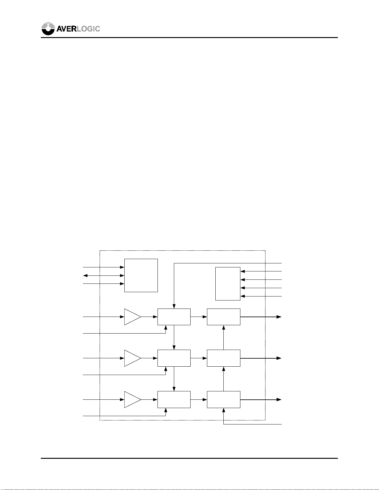
ADDR1/2
SDA
SCL
RIN
VRT
VN
VRB
GIN
VRT
VN
VRB
BIN
VRT
VN
VRB
IIC Interface
&
Control Logic
AL875-01a functional block diagram.vsd
CKEXT
HSYNC
Digital
Logic
Circuits
ADC/RT/H
ADC/GT/H
ADC/BT/H
Output
Logic
Output
Logic
Output
Logic
VSYNC
CK REF
CP
ROUT<7:0>
GOUT<7:0>
BOUT<7:0>
/OE
Preliminary version subject to change without notice January 25, 2001 4

AL875
3.0 General Description
The AL875 is a high-speed triple 8-bit monolithic analog-to-digital converter (ADC) designed for
digitizing RGB graphics/video signal or other applications. Its 110 MHz conversion rate can support
display resolution of up to 1280x1024 at 60Hz refresh rate.
The AL875 accepts 0.6~2.0V analog input range without using pre-amplifiers which may reduce the
overall S/N ratio. Digitized data is piped at the full clock rate to the 24-bit output port. The AL875
uses 3.3V power with 5V tolerant I/O and low power dissipation.
The sampling clock is provided by an external clock source, usually a PLL, which multiplies the
frequency of the input reference clock (usually a HSYNC signal) to generate the sampling clock. The
AL875 provides a programmable PLL divider up to 4096.
In addition, the input active horizontal and vertical starting and ending positions can be detected to
ensure that the whole picture fits into the displayable region of the screen. Through an I2C interface,
the AL875 is fully programmable to support various graphic resolutions.
Preliminary version subject to change without notice January 25, 2001 5
AL875
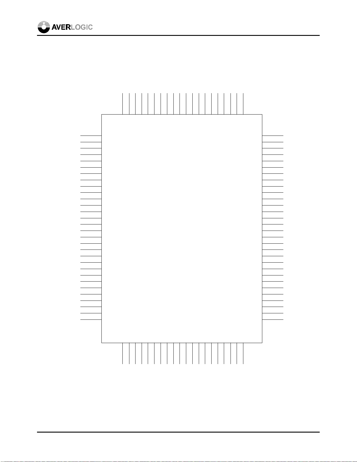
4.0 Pinout Diagrams
100
GND
VDDAPLLNCCP
99989796959493929190898887868584838281
GNDAPLL
VDD
CKREF
VSYNC
CKEXT
INV
HSYNC
HSFB
PWRDN
/OE
GND
VDDPLL
CKADCO
CKBO
GNDPLL
CKAO
1
2
3
4
5
6
7
8
9
10
11
12
13
14
15
16
17
18
19
20
21
22
23
24
25
26
27
28
29
30
TESTIN3
TESTIN2
TESTIN1
TESTIN0
VDD
VRBR
VNR
VRTR
NC
NC
VDDAR
RIN
GNDAR
VRBG
VNG
VRTG
NC
NC
VDDAG
GIN
GNDAG
VRBB
VNB
VRTB
NC
NC
VDDAB
BIN
GNDAB
ADTEST3
CKINTEN
RCLAMP
ADDR134ADDR2
AL875
ADTEST1
ADTEST2
VDD
SDA
GND
TESTIN4
SCL
/RESET
ROF
GOF
BOF
BOUT0
GNDB
CKREFO
VDDR
ROUT7
ROUT6
ROUT5
ROUT4
ROUT3
ROUT2
ROUT1
ROUT0
GNDR
VDDG
GOUT7
GOUT6
GOUT5
GOUT4
GOUT3
GOUT2
GOUT1
GOUT0
GNDG
VDDB
BOUT7
BOUT6
BOUT5
BOUT4
BOUT3
BOUT2
BOUT1
BCLAMP
GCLAMP
80
79
78
77
76
75
74
73
72
71
70
69
68
67
66
65
64
63
62
61
60
59
58
57
56
55
54
53
52
51
31
32
33
35
36
37NC38NC39
AL875-03 pinout diagram
40
41
42
43
44
45
46
47
48
49
50
Preliminary version subject to change without notice January 25, 2001 6
AL875
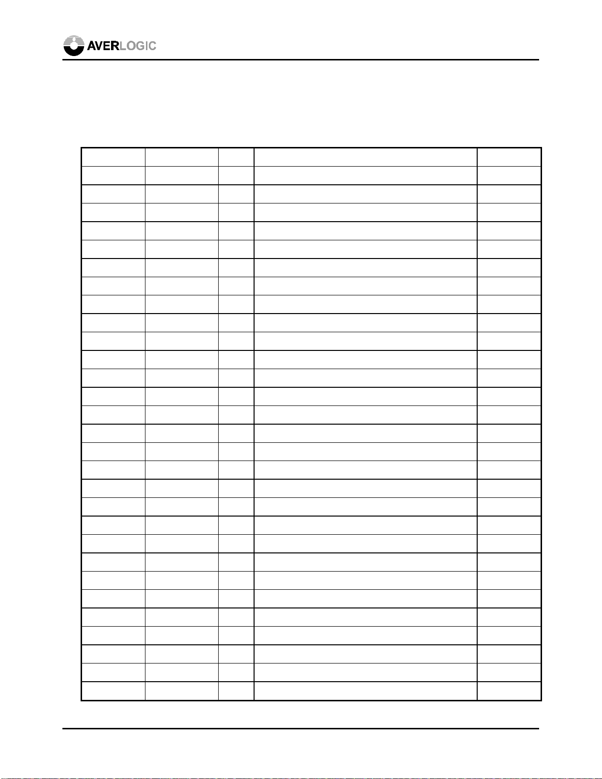
5.0 Pin Definition and Description
Following is the pin definition of the AL875 with the corresponding TDA8752 pin assignment
attached.
AL875 Type PIN# DESCRIPTION TDA8752
TESTIN3 IN (CMOS) 1 Test signal input 3, can be left open. n.c.
TESTIN2 IN (CMOS) 2 Test signal input 2, can be left open. DEC2
TESTIN1 IN (CMOS) 3 Test signal input 1, can be left open. Vref
TESTIN0 IN (CMOS) 4 Test signal input 0, can be left open. DEC1
VDD POWER 5 Digital power supply n.c.
VRBR IN 6 Red channel bottom voltage reference RAGC
VNR IN 7 Red channel comparator voltage reference RBOT
VRTR IN 8 Red channel top voltage reference RGAINC
NC -- 9 Not connected RCLP
NC -- 10 Not connected RDEC
VDDAR POWER 11 Red channel analog power supply VCCAR
RIN IN 12 Red channel analog input RIN
GNDAR GROUND 13 Red channel analog ground AGNDR
VRBG IN 14 Green channel bottom voltage reference GAGC
VNG IN 15 Green channel comparator voltage reference GBOT
VRTG IN 16 Green channel top voltage reference GGAINC
NC -- 17 Not connected GCLP
NC -- 18 Not connected GDEC
VDDAG POWER 19 Green channel analog power supply VCCAG
GIN IN 20 Green channel analog input GIN
GNDAG GROUND 21 Green channel analog ground AGNDG
VRBB IN 22 Blue channel bottom voltage reference BAGC
VNB IN 23 Blue channel comparator voltage reference BBOT
VRTB IN 24 Blue channel top voltage reference BGAINC
NC -- 25 Not connected BCLP
NC -- 26 Not connected BDEC
VDDAB POWER 27 Blue channel analog power supply VCCAB
BIN IN 28 Blue channel analog input BIN
GNDAB GROUND 29 Blue channel analog ground AGNDB
Preliminary version subject to change without notice January 25, 2001 7
AL875
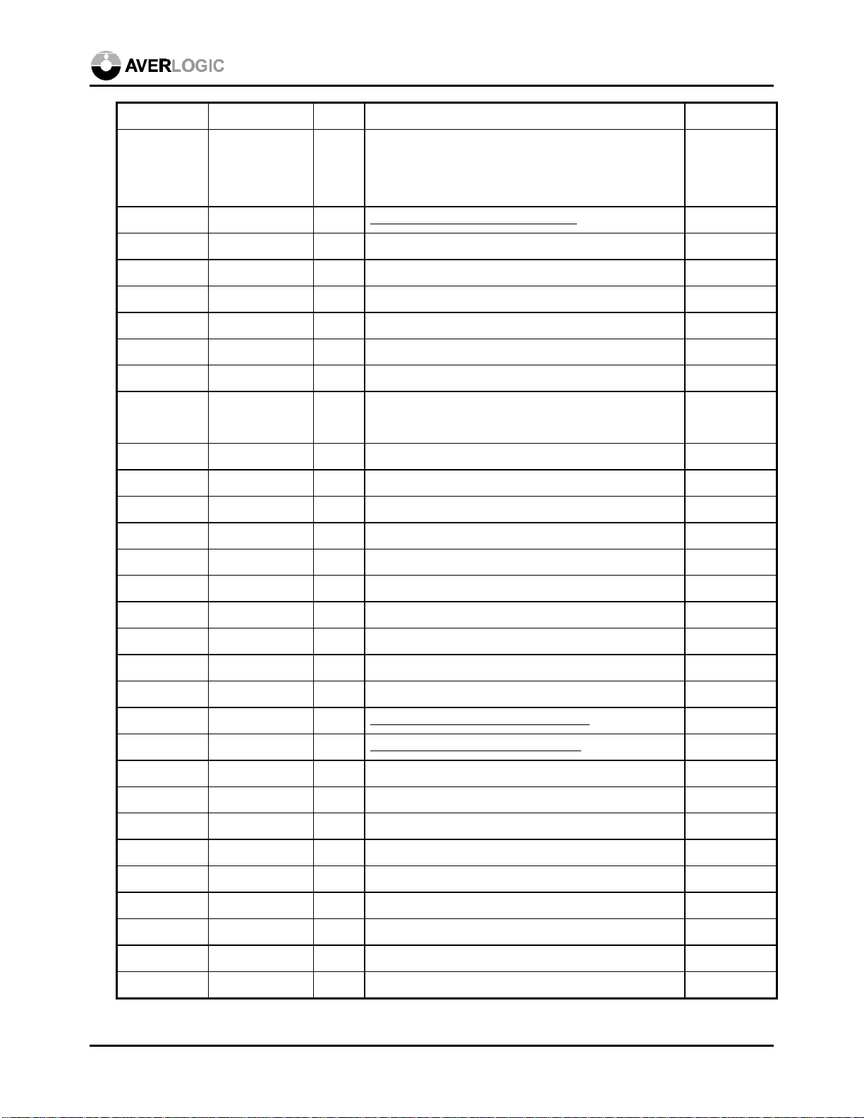
ADTEST3 IN (CMOSu) 30 Internal ADC test pin 3, to be pulled up. n.c.
CKINTEN IN (CMOSd) 31 Test pin, pulled down for normal operation.
n.c.
Reserved for AL876 internal clock enable (LO:
external clock, HI: internal PLL clock)
RCLAMP OUT (CMOSt) 32 Red channel clamp control output (NC) I2C/3W
ADDR1 IN (CMOSd) 33 I2C address control input 1 ADD1
ADDR2 IN (CMOSd) 34 I2C address control input 2 ADD2
ADTEST1 IN (CMOSd) 35 Internal ADC test pin 1, to be pulled down. TCK
ADTEST2 IN (CMOSd) 36 Internal ADC test pin 2, to be pulled down. TDO
NC -- 37 Not connected DIS
NC -- 38 Not connected SEN
SDA INOUT
39 I2C serial data input/output SDA
(CMOSsu)
VDD POWER 40 Logic digital power supply VDDD
GND GROUND 41 Logic digital ground VSSD
SCL IN (CMOSs) 42 I2C serial clock input SCL
TESTIN4 IN (CMOSd) 43 Test signal input 4, to be pulled up n.c.
/RESET IN (CMOSu) 44 Reset pin (active LOW) n.c.
ROF OUT (CMOS) 45 Red channel ADC output overflow ROR
GOF OUT (CMOS) 46 Green channel ADC output overflow GOR
BOF OUT (CMOS) 47 Blue channel ADC output overflow BOR
GNDB GROUND 48 Blue channel ADC output ground OGNDB
BOUT0 OUT (CMOSt) 49 Blue channel ADC output bit 0 B0
GCLAMP OUT (CMOSt)
BCLAMP OUT (CMOSt) 51 Blue channel clamp control output (NC) n.c.
Green channel clamp control output (NC) n.c.
BOUT1 OUT (CMOSt) 52 Blue channel ADC output bit 1 B1
BOUT2 OUT (CMOSt) 53 Blue channel ADC output bit 2 B2
BOUT3 OUT (CMOSt) 54 Blue channel ADC output bit 3 B3
BOUT4 OUT (CMOSt) 55 Blue channel ADC output bit 4 B4
BOUT5 OUT (CMOSt) 56 Blue channel ADC output bit 5 B5
BOUT6 OUT (CMOSt) 57 Blue channel ADC output bit 6 B6
BOUT7 OUT (CMOSt) 58 Blue channel ADC output bit 7 B7
VDDB POWER 59 Blue channel ADC output power supply VCCOB
GNDG GROUND 60 Green channel ADC output ground OGNDG
Preliminary version subject to change without notice January 25, 2001 8
AL875
GOUT0 OUT (CMOSt) 61 Green channel ADC output bit 0 G0
GOUT1 OUT (CMOSt) 62 Green channel ADC output bit 1 G1
GOUT2 OUT (CMOSt) 63 Green channel ADC output bit 2 G2
GOUT3 OUT (CMOSt) 64 Green channel ADC output bit 3 G3
GOUT4 OUT (CMOSt) 65 Green channel ADC output bit 4 G4
GOUT5 OUT (CMOSt) 66 Green channel ADC output bit 5 G5
GOUT6 OUT (CMOSt) 67 Green channel ADC output bit 6 G6
GOUT7 OUT (CMOSt) 68 Green channel ADC output bit 7 G7
VDDG POWER 69 Green channel ADC output power supply VCCOG
GNDR GROUND 70 Red channel ADC output ground OGNDR
ROUT0 OUT (CMOSt) 71 Red channel ADC output bit 0 R0
ROUT1 OUT (CMOSt) 72 Red channel ADC output bit 1 R1
ROUT2 OUT (CMOSt) 73 Red channel ADC output bit 2 R2
ROUT3 OUT (CMOSt) 74 Red channel ADC output bit 3 R3
ROUT4 OUT (CMOSt) 75 Red channel ADC output bit 4 R4
ROUT5 OUT (CMOSt) 76 Red channel ADC output bit 5 R5
ROUT6 OUT (CMOSt) 77 Red channel ADC output bit 6 R6
ROUT7 OUT (CMOSt) 78 Red channel ADC output bit 7 R7
VDDR POWER 79 Red channel ADC output power supply VCCOR
CKREFO OUT (CMOS) 80 PLL Reference clock output with phase
CKREFO
adjustment from CKREF. Usually used for
external PLL reference input.
CKAO OUT (CMOS) 81 Output clock A (in phase with the internal digital
CKAO
logic clock)
GNDPLL GROUND 82 Digital ground. Reserved for AL876 PLL digital
OGNDPLL
ground.
CKBO OUT (CMOS) 83 Output clock B (with phase adjustment) CKBO
CKADCO OUT (CMOS) 84 ADC sampling clock (in phase with the ADC
CKADCO
sampling clock)
VDDPLL POWER 85 Digital power supply. Reserved for AL876 PLL
VCCO(PLL)
digital power supply. Suggested to be separated
from the other VDD pins with a ferrite bead for
AL876 compatibility
GND GROUND 86 Digital ground DGND
Preliminary version subject to change without notice January 25, 2001 9

AL875
/OE IN (CMOS) 87 Output enable (when OE is HIGH, the outputs are
in HI-Z)
PWRDN IN (CMOSd) 88 Power-Down control (Active HIGH) PWOFF
HSFB OUT (CMOS) 89 Clock feedback divider output. Used with optional
external PLL
HSYNC IN (CMOS) 90 Horizontal sync input HSYNC
INV IN (CMOSd) 91 The invert control of the ADC sampling clock INV
CKEXT IN (CMOS) 92 External clock input CKEXT
VSYNC IN (CMOS) 93 Vertical sync input COAST
CKREF IN (CMOS) 94 PLL reference clock input CKREF
VDD POWER 95 Digital power supply VCCD
GNDAPLL GROUND 96 Analog ground. Reserved for AL876 PLL analog
ground.
CP IN 97 Internal compensation pin. Reserved for AL876
PLL filter input. Please follow the reference
design for external RC filter circuitry.
OE
CLP
AGNDPLL
CP
NC -- 98 Not connected CZ
VDDAPLL POWER 99 Analog power supply. Reserved for AL876 PLL
analog power supply. Suggested to be separated
from the other VDD pins with a ferrite bead for
AL876 compatibility
GND GROUND 100 Digital ground n.c.
VCCAPLL
Remarks:
• CMOSd: CMOS with internal pull-down
• CMOSs: CMOS with Schmitt trigger input
• CMOSsu: CMOS with Schmitt trigger input and internal pull-up
• CMOSt: CMOS with tri-state output
• CMOSu: CMOS with internal pull-up
Note: Clamping feature is not supported in the chip.
Pin list grouped by functionality
Symbol Type PIN# DESCRIPTION
Analog Input
RIN IN 12 Red channel analog input
Preliminary version subject to change without notice January 25, 2001 10
AL875
GIN IN 20 Green channel analog input
BIN IN 28 Blue channel analog input
VRTR IN 8 Red channel top voltage reference
VRTG IN 16 Green channel top voltage reference
VRTB IN 24 Blue channel top voltage reference
VNR IN 7 Red channel comparator voltage reference
VNG IN 15 Green channel comparator voltage reference
VNB IN 23 Blue channel comparator voltage reference
VRBR IN 6 Red channel bottom voltage reference
VRBG IN 14 Green channel bottom voltage reference
VRBB IN 22 Blue channel bottom voltage reference
Digital Output
ROUT[7:0] OUT (CMOSt) 78-71 Red channel ADC output
GOUT[7:0] OUT (CMOSt) 68-61 Green channel ADC output
BOUT[7:0] OUT (CMOSt) 58-52, 49 Blue channel ADC output
ROF OUT (CMOS) 45 Red channel ADC output overflow
GOF OUT (CMOS) 46 Green channel ADC output overflow
BOF OUT (CMOS) 47 Blue channel ADC output overflow
RCLAMP OUT (CMOSt) 32 Red channel clamp control output(NC)
GCLAMP OUT (CMOSt) 50 Green channel clamp control output(NC)
BCLAMP OUT (CMOSt) 51 Blue channel clamp control output(NC)
Clock Pins (and reserved PLL pins for the AL876)
HSYNC IN (CMOS) 90 Horizontal sync input
VSYNC IN (CMOS) 93 Vertical sync input
CKREF IN (CMOS) 94 PLL reference clock input, which is usually
HSYNC
CKEXT IN (CMOS) 92 External clock input
CP IN 97 Internal compensation pin. Reserved for AL876
PLL filter input. Please follow the reference
design for external RC filter circuitry.
CKREFO OUT (CMOS) 80 PLL Reference clock output with phase
adjustment from CKREF. Usually used for
external PLL reference input.
CKAO OUT (CMOS) 81 Output clock A (in phase with internal digital
Preliminary version subject to change without notice January 25, 2001 11
 Loading...