AVER AL422V5, AL422V3, AL422B Datasheet

AL422 Data Sheets
(Revision V1.1)

AL422
Amendments (Since April 2, 1999)
05-13-99 DC/AC characteristics (including current consumption) updated.
07-02-99 Pinout diagram (5.0) and DC external load (7.4) modified.
08-03-99 Description about TST pin added in sections 6.0 & 8.1.
09-02-99 8.3.2 rewritten.
10-26-99 Capacitance provided in the AC characteristics section.
12-15-99 Remove TST pin restriction.
01-18-01 1. Revised section “8.3.2 Read Enable during Reset Cycles” to “8.3.2 The Proper
Manipulation of FIFO Access”.
2. Add section “8.3.3 Single Field Write with Multiple Read Operation”
3. Add section “8.3.4 One Field Delay Line (The Old Data Read)”
AL422B January 23, 2001 2

AL422
AL422 3M-Bits FIFO Field Memory
Contents:
1.0 Description ________________________________________________________________ 4
2.0 Features___________________________________________________________________ 4
3.0 Applications ________________________________________________________________ 4
4.0 Ordering Information________________________________________________________ 4
5.0 Pinout Diagram ____________________________________________________________ 5
6.0 Pin Description _____________________________________________________________ 5
7.0 Electrical Characteristics _____________________________________________________ 6
7.1 Absolute Maximum Ratings________________________________________________________ 6
7.2 Recommended Operating Conditions ________________________________________________ 6
7.3 DC Characteristics _______________________________________________________________ 6
7.4 AC Characteristics _______________________________________________________________ 7
7.5 Timing Diagrams_________________________________________________________________ 9
8.0 Functional Description______________________________________________________ 13
8.1 Memory Operation______________________________________________________________ 14
8.2 5V and 3.3V applications _________________________________________________________ 15
8.3 Application Notes _______________________________________________________________ 16
8.3.1 Irregular Read/Write _________________________________________________________________ 16
8.3.2 The Proper Manipulation of FIFO Access_________________________________________________ 17
8.3.3 Single Field Write with Multiple Read Operation___________________________________________ 17
8.3.4 One Field Delay Line (The Old Data Read) _______________________________________________ 17
9.0 Mechanical Drawing _______________________________________________________ 19
AL422B January 23, 2001 3

AL422
1.0 Description
The AL422 consists of 3M-bits of DRAM, and is configured as 393,216 words x 8 bit FIFO (first in
first out). The interface is very user-friendly since all complicated DRAM operations are already
managed by the internal DRAM controller.
Current sources of similar memory (field memory) in the market provide limited memory size which
is only enough for holding one TV field, but not enough to hold a whole PC video frame which
normally contains 640x480 or 720x480 bytes. The AverLogic AL422 provides 50% more memory
to support high resolution for digital PC graphics or video applications. The 50% increase in speed
also expands the range of applications.
2.0 Features
• 384K (393,216) x 8 bits FIFO organization
• Support VGA, CCIR, NTSC, PAL and
HDTV resolutions
• Independent read/write operations (different
I/O data rates acceptable)
• High speed asynchronous serial access
• Read/write cycle time: 20ns
• Access time: 15ns
• Output enable control (data skipping)
• Self refresh
• 5V or 3.3V power supply
• Standard 28-pin SOP package
4.0 Ordering Information
3.0 Applications
• Multimedia systems
• Video capture systems
• Video editing systems
• Scan rate converters
• TV’s picture in picture feature
• Time base correction (TBC)
• Frame synchronizer
• Digital video camera
• Buffer for communications systems
Part number Package Power Supply Status
AL422B 28-pin plastic SOP +5/+3.3 volt Shipping
AL422V5 28-pin plastic SOP +5 volt Replaced by AL422B
AL422V3 28-pin plastic SOP +3.3 volt Replaced by AL422B
AL422B January 23, 2001 4

AL422
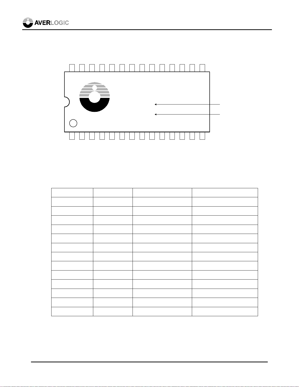
5.0 Pinout Diagram
DO1 DO2 DO3 /RE
DO0
28 27 26
2 3 4 5
1
DI1 DI2 DI3 /WE
DI0
25 24
6.0 Pin Description
Pin name Pin # I/O type Function
/OE /RRST RCK DEC
GND
22 21 20 19
23
AVERLOGIC
AL422B
XXXXX
XXXX
7 8 9 10
6
TST /WRST WCK VDD
GND
DO5 DO6 DO7
DO4
17 16 15
18
12 13 14
11
DI5 DI6 DI7
DI4
AL422-04 422B pinout diagram
Lot Number
Date Code
DI0~DI7 1~4, 11~14 input Data input
WCK 9 Input Write clock
/WE 5 Input (active low) Write enable
/WRST 8 Input (active low) Write reset
DO0~DO7 15~18, 25~28 Output (tristate) Data output
RCK 20 Input Read clock
/RE 24 Input (active low) Read enable
/RRST 21 Input (active low) Read reset
/OE 22 Input (active low) Output enable
TST 7 Input Test pin (pulled-down)*
VDD 10 5V or 3.3V
DEC/VDD 19 Decoupling cap input
GND 6, 23 Ground
AL422B January 23, 2001 5

AL422
7.0 Electrical Characteristics
7.1 Absolute Maximum Ratings
Parameter
Ratings
3.3V application 5V application
VDD Supply Voltage -1.0 ~ +4.5 -1.0 ~ +7.0 V
VP Pin Voltage -1.0 ~ +5.5 -1.0 ~ VDD +0.5 V
IO Output Current -20 ~ +20 -20 ~ +20 mA
T
Ambient Op. Temperature 0 ~ +70 0 ~ +70 °C
AMB
T
Storage temperature -55 ~ +125 -55 ~ +125 °C
stg
7.2 Recommended Operating Conditions
Parameter
VDD Supply Voltage +3.0 +3.6 +4.5 +5.25 V
VIH High Level Input Voltage +2.0 +5.5 +3.0 VDD +0.5 V
VIL Low Level Input Voltage -1.0 +0.8 -1.0 +0.8 V
3.3V application 5V application
Min Max Min Max
Unit
Unit
7.3 DC Characteristics
(VDD =5V or 3.3V, Vss=0V. T
Parameter
IDD Operating Current @20MHz - 33 - - 50 - mA
IDD Operating Current @30MHz - 45 - - 66 - mA
IDD Operating Current @40MHz - 57 - - 82 - mA
IDD Operating Current @50MHz - 68 - - 97 - mA
I
Standby Current - 7 - - 12 - mA
DDS
VOH Hi-level Output Voltage 0.7V
VOL Lo-level Output Voltage - - +0.4 - - +0.4 V
ILI Input Leakage Current -10 - +10 -10 - +10
ILO Output Leakage Current -10 - +10 -10 - +10
AL422B January 23, 2001 6
= 0 to 70°C)
AMB
3.3V application 5V application
Min Typ Max Min Typ Max
DD
- VDD +3.0 - VDD V
Unit
µA
µA
 Loading...