

AVER AL300 Datasheet

AL300 Data Sheets
Version 2.0

AL300
Amendments (Since April 2, 1999)
04.02.99 “Section 6.13 Zoom” is added to the document.
04.15.99 Pin 131 is redefined as a GND pin instead of a NC pin. Sections 4.0 and 5.0 are modified
accordingly.
05.11.99 Power consumption data and Programming flowchart are provided.
05.12.99 Registers #06h, 07h, 1Bh, 36h, 4Eh, 50~57h, 66h, 67h, 71h, 85h, 86h, 89h and 8Ah are
modified due to the ver. B change. VIH modified.
05.26.99 Pin definition of R/YIN<7:0>, G/UVIN<7:0> and BIN<7:0> is modified to reflect ver. B
change.
06.15.99 Pin definition of odd and even output replaced by B and A.
07.02.99 Register table and some description added and updated.
07.13.99 Added more PLL description in section 6.4 and the register definition 10h and 11h.
08.03.99 Definition of registers 80h, 84h and 88h modified.
08.25.99 Definition of registers 06h, 80h modified. Definition of registers 05h, 19h, 1Ah, 3Bh and
3Ch modified. Description of #17h and #18h modified.
9.15.99 Added section 6.14, Initialization, modified section 6.7.
9.29.99 Registers #80h and #82h modified to reflect version B-0 change.
10.5.99 Section 10.0 Power consumption updated
8.17.00 Diagram AL300-11 in section “6.11.2 ROM mode” and definition of register 13h & 35h
are modified.
6.27.01 Version 2.0, removed CCIR-656 8-bit interface support from data sheets and add timing
diagram
November 28, 2001 2

AL300
Contents
1.0 Features________________________ 4
2.0 Applications _____________________ 4
3.0 General Description ______________ 5
4.0 Pinout Diagrams_________________ 6
5.0 Pin Definition and Description _____ 7
6.0 Functional Description___________ 12
6.1 Input Data Format _______________ 12
6.2 Scan Mode Detection _____________ 13
6.3 Automatic Positioning Control______ 14
6.4 Output Clock PLL _______________ 14
6.5 Input/Capture Timing_____________ 17
6.6 Output/Display Timing____________ 18
6.7 Internal Timing Generator _________ 19
6.8 Zoom Engine ____________________ 20
6.9 Operating Modes ________________ 20
6.9.1 Non-interlaced Zoom Mode _________20
6.9.2 De-interlaced Zoom Mode __________20
6.9.3 Bypass Mode_____________________21
6.10 Interrupt ______________________ 21
6.11 On Screen Display (OSD)_________ 21
6.11.1 RAM mode_____________________23
6.11.2 ROM mode_____________________23
6.11.3 OSD Timing____________________24
6.11.4 OSD Bitmap/Font Formatting ______25
6.12 Output Data Format_____________ 27
6.13 Zoom _________________________ 27
6.14 Initialization____________________ 28
6.15 I2C Programming _______________ 28
7.0 Electrical Characteristics _________ 31
7.1 Recommended Operating Conditions 31
7.2 Characteristics __________________ 31
8.0 AL300 Register Definition ________ 33
8.1 Register Description ______________ 37
8.2 Programming Flowchart ___________ 61
9.0 Mechanical Drawing _____________ 61
9.0 Mechanical Drawing ______________ 62
10.0 Power Consumption ____________ 63
7.3 Timing Diagram _________________ 32
November 28, 2001 3
AL300
AL300
LCD Monitor Controller
1.0 Features
• Converts PC’s or TV’s signals for flat panel
displays
• Supports active matrix up to 1280x1024
resolution
• De-interlacing support for video inputs
• Automatic screen positioning support
• Fully programmable zoom ratios
• Independent linear zoom in H and V
directions
• Supports single and dual pixel per clock
panels
• Dithering logic to enhance color resolution
for 12-bit or 18-bit panels
• Built-in high speed PLL
• User-definable font table supporting different
languages and font sizes
• Two built-in OSD windows
• I2C programmable
• No external memory required
• Single 3.3 volt power with 5 volt tolerant I/O
• 160-pin 28x28 mm PQFP package
2.0 Applications
• TFT LCD Monitor
• LCD TV
• LCD Projector with PC and/or TV Input
• Other Flat Panel Displays
• TV to PC Monitor Scan Converter
• Progressive Scan TV
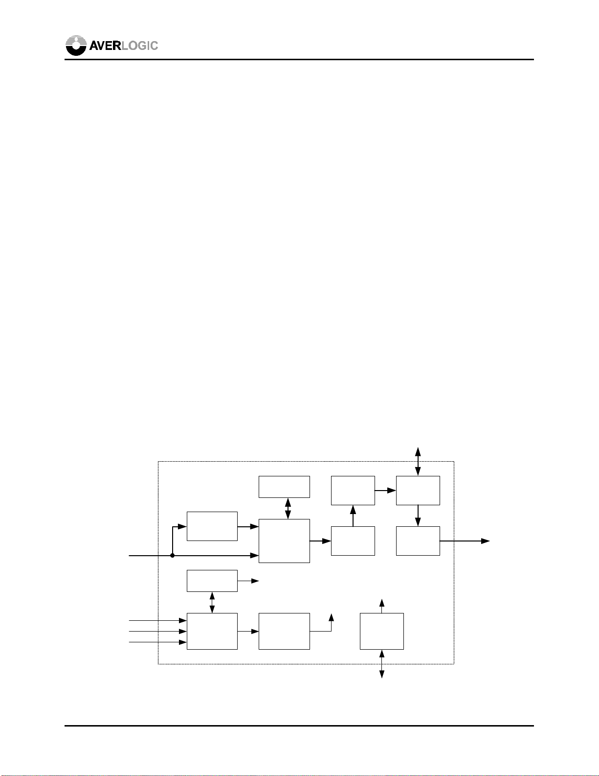
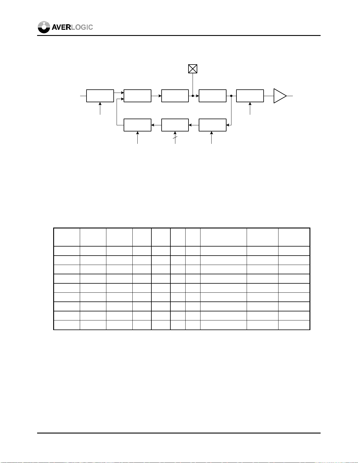
Font Table ROM
Memory
Color Space
Converter
Input Video/
Graphics
Data
PLL
HSYNC
VSYNC
CLK
November 28, 2001 4
Scan Mode
Detection
AL300-01 Functional Block Diagram
Zoom
Engine
OCLK
Timing
Generator
Dithering OSD
Gamma
LUT
Control
Control
Timing
Registers
IIC
Interface
Microcontroller
Panel
Interface
Panel

AL300
3.0 General Description
The AL300 is designed to enable simple connection from PC’s or video devices to flat panel displays.
It provides LCD/PDP monitor and projector manufacturers with a low-cost, easy solution to bring TV
or PC video to LCD panels.
The AL300 is equipped with a high quality zoom engine that automatically maintains full screen
output display, regardless of the resolution of the incoming signal. The input video can be linearly and
independently zoomed in the x and y directions. The AL300 also provides de-interlacing, filtering, and
scaling support for interlaced video to be displayed on a LCD panel.
Two integrated On Screen Display (OSD) windows provide overlay of a control menu, text, or
caption on the output display. With the internal OSD RAM, OSD bitmaps of up to 8K pixels are
supported. With optional external user-defined font table ROM, the AL300 OSD functionality is very
flexible with font size and display location; virtually all languages and fonts are supported. Special
OSD effects such as translucency and blinking offer the manufacturer a unique and vivid way of
presenting monitor status, control menu, or other display information.
Used with an AL875 (high speed 3-channel ADC with PLL, 100-pin QFP), the AL300 (in 160-pin
QFP) offers the best cost-performance and total solution for LCD monitors or projectors, or other flat
panel devices.
November 28, 2001 5
AL300
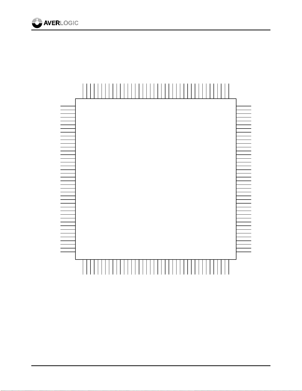
4.0 Pinout Diagrams
BA0
BA1
BA2
BA3
BA4
BA5
VCC
BA6
BA7
GA0
VCC
GA1
GA2
GA3
GA4
GND
GA5
GA6
GA7
RA0
GND
RA1
RA2
RA3
RA4
VCC
RA5
RA6
RA7
VCC
PDSPEN
PVS
PHS
GND
SCLK
PCLKB
PCLKA
GOUT3
GOUT2
GOUT1
VCC
RESETB
IHSREF
OHSREF
OHSFB
OCLK
OPLLCLK
PLLVCC
VCOIN
PLLGND
GND
ROMDATA7
ROMDATA6
ROMDATA5
ROMDATA4
GND
ROMDATA3
ROMDATA2
ROMDATA1
ROMDATA0
VCC
ROMADDR0
ROMADDR1
ROMADDR2
ROMADDR3
GND
ROMADDR4
ROMADDR5
ROMADDR6
ROMADDR7
VCC
ROMADDR8
ROMADDR9
ROMADDR10
ROMADDR11
ROMADDR12
ROMADDR13
ROMADDR14
ROMADDR15
GND
121
122
123
124
125
126
127
128
129
130
131
132
133
134
135
136
137
138
139
140
141
142
143
144
145
146
147
148
149
150
151
152
153
154
155
156
157
158
159
160
120
119
118
117
116
115
114
113
112
111
110
109
108
107
106
105
104
103
102
101
100
AL300
A-1
99989796959493929190898887868584838281
80
79
78
77
76
75
74
73
72
71
70
69
68
67
66
65
64
63
62
61
60
59
58
57
56
55
54
53
52
51
50
49
48
47
46
45
44
43
42
41
BB0
BB1
BB2
BB3
GND
BB4
BB5
BB6
BB7
GND
GB0
GB1
GB2
GB3
VCC
GB4
GB5
GB6
GB7
VCC
RB0
RB1
RB2
RB3
GND
RB4
RB5
RB6
RB7
VCC
Test2
Test1
YUVIN
I2CADDR
PWRDN
GND
NC
SDA
SCL
IREQ
1
2
3
4
5
6
7
8
9
10
11
12
13
14
15
16
17
18
19
TVVS
TVCLK
TVHREF
GND
TVHS
GVS
GHS
GND
GCLK
GHREF
RIN7/YIN7
RIN6/YIN6
RIN5/YIN5
RIN4/YIN4
RIN3/YIN3
RIN2/YIN2
RIN1/YIN1
RIN0/YIN0
202122232425262728
VCC
GIN7/UVIN7
GIN6/UVIN6
GIN5/UVIN5
GIN4/UVIN4
GIN3/UVIN3
293031323334353637
BIN7
GND
GIN2/UVIN2
GIN1/UVIN1
GIN0/UVIN0
BIN6
BIN5
BIN4
BIN3
BIN2
BIN1
VCC
BIN0
38
39
40
XIN
XOUT
HOSTCLK
AL300 pinout diagram
November 28, 2001 6
AL300
5.0 Pin Definition and Description
Following is the pin definition of the AL300:
Pin Name Type Pin # Note
Video Interface
TVCLK IN (CMOSd) 1 Video Clock from Video Source
TVHREF IN (CMOSd) 2 Video Horizontal Active Data Reference
This signal is used to indicate valid data of the YUV
input.
TVVS IN (CMOSs) 3 Video Vertical Sync Signal
TVHS IN (CMOSs) 4 Video Horizontal Sync Signal
Graphic Interface
GVS IN (CMOSs) 6 Graphic Vertical Sync Signal
GHS IN (CMOSs) 7 Graphic Horizontal Sync Signal
GHREF IN (CMOS) 8 Graphic Horizontal Active Data Reference
GCLK IN (CMOSd) 9 Graphic Input Clock
R/YIN<7:0> IN (CMOS) 11-18 Red Input When in RGB Mode
Y Input When in CCIR601 422 and 444 Modes
G/UVIN<7:0> IN (CMOS) 20-27 Green Input When in RGB Mode
CbCr Input When in CCIR601 422 Mode
Cb Input When in CCIR601 444 Mode
Refer to register #1Bh for details.
BIN<7:0> IN (CMOS) 29-36 Blue Input When in RGB Mode
Cr Input When in CCIR601 444 Mode
Refer to register #1Bh for details.
Host Interface
HOSTCLK OUT (CMOS) 38 Buffered Output of the Clock Input for Host Interface
such as a Micro-controller
XOUT OUT (CMOS) 39 Crystal Output
XIN IN (CMOS) 40 Crystal Input; the frequency provided is for I2C
sampling and for output reference timing when input
sync signals are missing or undetectable. Usually in
the range of 10~50MHz. Refer to section 6.7 Internal
Timing Generator for details.
November 28, 2001 7
AL300
IREQ OUT (CMOS) 41 Interrupt Request, active high
SCL IN (CMOSs) 42 I2C Serial Clock Input
SDA INOUT
43 I2C Serial Data Input/Output
(COMSsu)
GOUT1 OUT (CMOS) 81 General Purpose Output
Connected to Register 0x1B bit 2
GOUT2 OUT (CMOS) 82 General Purpose Output
Connected to Register 0x1B bit 3
GOUT3 OUT (CMOS) 83 General Purpose Output
Connected to Register 0x1B bit 1
Configuration
PWRDN IN (CMOSd) 46 Power Down
0, Normal Operation
1, Power Down
I2CADDR IN (CMOSd) 47 I2C Bus Slave Address Select
0, write address = 70, read address = 71
1, write address = 72, read address = 73
YUVIN IN (CMOSd) 48 YUV Input
0, RGB Format Video Input
1, CCIR YUV Format Video Input
Refer to RIN, GIN, BIN pins
Test1 IN (CMOSd) 49 Test Pin
Test2 IN (CMOSd) 50 Test Pin
Panel/Display Interface
RB<7:0> OUT (CMOS) 52-55, 57-60 Right Pixel of Interleaved Red Output in Dual Pixel
Mode
Valid when Register 0x43 bit4 = ‘1’.
Data are output with PCLKB.
For AL300 ver. A, the B data lag A data by 90° (half
SCLK).
For AL300 ver. B, A and B data are aligned.
GB<7:0> OUT (CMOS) 62-65, 67-70 Right Pixel of Interleaved Green Output in Dual Pixel
Mode
Valid when Register 0x43 bit4 = ‘1’.
Data are output with PCLKB.
November 28, 2001 8
AL300
For AL300 ver. A, the B data lag A data by 90° (half
SCLK).
For AL300 ver. B, A and B data are aligned.
BB<7:0> OUT (CMOS) 72-75, 77-80 Right Pixel of Interleaved Blue Output in Dual Pixel
Mode
Valid when Register 0x43 bit4 = ‘1’.
Data are output with PCLKB.
For AL300 ver. A, the B data lag A data by 90° (half
SCLK).
For AL300 ver. B, A and B data are aligned.
PCLKA OUT (CMOS) 84 Leading Pixel Clock of Interleaved Video Output for
Right data in Dual Pixel Mode. Polarity is
programmable
PCLKB OUT (CMOS) 85 Lagging Pixel Clock of Interleaved Video Output for
Right data in Dual Pixel Mode. Polarity is
programmable.
Default PCLKB lags PCLKA by 180° (one SCLK).
SCLK OUT (CMOS) 86 Display Pixel Clock (for single pixel per clock mode)
PHS OUT (CMOS) 88 Panel/Display Hsync
Can be programmed to either polarity.
PVS OUT (CMOS) 89 Panel/Display Vsync
Can be programmed to either polarity.
PDSPEN OUT (CMOS) 90 Panel/Display Display Enable; used to indicate active
output pixels (HDE).
Can be programmed to either polarity.
RA<7:0> OUT (CMOS) 92-95, 97-100 Red Data Output
When Register 0x43 bit4 = ‘0’, data are output every
SCLK.
When Register 0x43 bit4 = ‘1’, the left pixel of
interleaved red data are output with PCLKA.
GA<7:0> OUT (CMOS) 102-105, 107-
Green Data Output
110
When Register 0x43 bit4 = ‘0’, data are output every
SCLK.
When Register 0x43 bit4 = ‘1’, the left pixel of
interleaved red data are output with PCLKA.
November 28, 2001 9
AL300
BA<7:0> OUT (CMOS) 112-115, 117-
120
Blue Data Output
When Register 0x43 bit4 = ‘0’, data are output every
SCLK.
When Register 0x43 bit4 = ‘1’, the left pixel of
interleaved red data are output with PCLKA.
PLL (Phase Lock Loop) Interface
IHSREF OUT (CMOS) 123 Input Hsync Reference, buffered and polarity adjusted,
usually for input PLL to regenerate input pixel clock.
Always positive polarity.
When no input HSYNC is present, virtual IHSREF
can be generated by programming registers 41h & 42h
OHSREF OUT (CMOS) 124 Output Hsync Reference, for output PLL to generate
output pixel clock.
Always positive polarity.
OHSREF is either equivalent to IHSREF or the
equally divided IHSREF. Refer to registers 03h,
10h~13h.
OHSFB OUT (CMOS) 125 Output PLL Feedback; works with OHSREF to
generate output pixel clock
OCLK IN (CMOSd) 126 Output Clock, connected to OPLLCLK when internal
PLL is used; connected to external PLL clock output
when external PLL is used
OPLLCLK OUT (CMOS) 127 Recovered Output Clock generated by the internal PLL
VCOIN IN 129 PLL External VCO Filter Circuit Input
OSD ROM Interface
ROMDATA
<7:0>
ROMADDR
<15:0>
IN (CMOSd) 132-135, 137-
140
OUT (CMOS) 160-157, 155-
152, 150-147,
OSD ROM Data
OSD ROM Address
145-142
Power, Ground, Reset
RESETB IN (CMOS) 122 Reset, active low
PLLVCC POWER 128 VCC of Internal PLL, 3.3V
PLLGND GROUND 130 GND of Internal PLL
VCC POWER 19, 37, 51, 61, Digital VCC, 3.3V
November 28, 2001 10

AL300
66, 91, 96,
111, 116, 121,
141, 151
GND GROUND 5, 10, 28, 45,
Digital Ground
56, 71, 76, 87,
101, 106, 131,
136, 146, 156
NC - 44 No connection
Remarks:
CMOSd: CMOS with internal pull-down
CMOSs: CMOS with Schmitt trigger
CMOSsu: CMOS with Schmitt trigger and internal pull-up
November 28, 2001 11

AL300
6.0 Functional Description
The AL300 provides a simple way of connecting video or graphic sources to a flat panel display such
as a LCD. A LCD panel normally supports only one fixed resolution of digital non-interlaced data
format; therefore, it can not be connected directly to a video source due to the difference in format.
Additionally, VGA or TV video usually are in analog format and can be of many different resolutions
and refresh rates. The AL300 is designed to change the various video/graphics formats into a fixed
data format to be accepted by a specific LCD panel.
The input video format can be 24-bit digital RGB or 16-bit digital YUV. Different video sources can
be connected to an AL300 via certain digitization devices. For example, analog NTSC/PAL/SECAM
can be connected to the AL300 via a digital video decoder. Analog VGA RGB signal can be
connected to the AL300 after a high-speed three-channel analog-to-digital converter (ADC), such as
the AL875. Alternatively, digital PC graphics can also be applied to the AL300 through a Panel Link
or LVDS (low voltage differential signal) receiver.
The scan rate and resolution of the incoming video are recognized by the scan mode detection circuits.
The detected mode information stored in the AL300 registers is read through the I2C bus by the
firmware. The firmware then will decide how to program the chip such that the input video can be
scaled up to fit into the full screen size of the display. To achieve this, the linear zoom engine needs to
be programmed to properly scale the input video to the desired output resolution. Also, the
frequency of the display clock generated from the internal PLL needs to be programmed to the correct
level.
After the digital data is scaled, optional dithering is performed to retain color resolution for LCD
panels that support only 12-bit or 18-bit color resolutions. The processed data is overlaid with
internal on-screen-display (OSD) for display status or control menu.
6.1 Input Data Format
The AL300 accepts three input data formats: 24-bit RGB, 16-bit CCIR601 422 and 24-bit CCIR601
444 data. The clock and sync signal pins are separate for RGB or YUV while the YUV data share the
same pins as the RGB data. The input video format is defined by the YUVIN pin. Diagram AL30006 Input Data Format shows how to connect the AL300 for each format.
November 28, 2001 12
AL300
AL300 Data (RGB 444)
24-bit Interface
Rout
Gout
Bout
Digital RGB 444 Input
Y
UV
8
8
8
AL300 Data (CCIR601 422)
16-bit Interface
8
8
R/Y[7:0]
G/UV[7:0]
B[7:0]
YUVIN0
AL300
R/Y[7:0]
G/UV[7:0]
B[7:0]
YUVIN1
AL300 Data (CCIR601 444)
24-bit Interface
Y R/Y[7:0]
U
V
8
8
8
G/UV[7:0]
B[7:0]
YUVIN1
Digtial YUV 422 Input
AL300
Digital YUV 444 Input
AL300
AL300-06 Input Data Format
YUV input data is selected when the YUVIN pin is high. This hardware pin can be disabled by
“SoftConfig” (in register #03h, GENERAL). When the bit is set to one, the input video format is
controlled by “VideoIn” (in register #02h, BOARDCONFIG). RGB input data is selected when the
YUVIN pin is low.
6.2 Scan Mode Detection
The resolution of the analog input is determined by two hardware registers, LINERATE (Reg. #61h
and #62h) and INVTOTAL (Reg. #63h and #64h), which store the detected input line rate and the
November 28, 2001 13

AL300
detected total number of vertical lines, respectively. The line rate and frame rate values can be
obtained by counting the clock provided from XIN pin and/or calculations and some calculations.
When the line rate of the input video changes, a programmable interrupt signal is sent out to the
micro-controller for mode setting or other controls. Details about this can be found in the Interrupt
section.
6.3 Automatic Positioning Control
The active video (horizontal and vertical) starting and ending positions are detected to ensure that the
whole picture fits into the displayable region of the screen. The threshold of the minimum active video
value is user-definable. Position detection can be performed for any row or column across the whole
screen and it is programmable. Related registers are:
HNUMBER (horizontal line number, Reg. #70h),
DATA_TH (data threshold, Reg. #71h),
HDE_ST (horizontal active start high and low, Reg. #72h and #73h),
HDE_END (horizontal active end high and low, Reg. #74h and #75h),
VCOLUMN (selected vertical column number, Reg. #79h),
VDE_ST (vertical active start high and low, Reg. #7Ah and #7Bh),
and VDE_END (vertical active end high and low, Reg. #7Ch and #7Dh).
Details about these registers can be found in the Register Definition section.
6.4 Output Clock PLL
The internal PLL can regenerate a display clock from the incoming horizontal sync signal. The
maximum multiplication factor (N) is 2047 defined by register PLLDIV (Reg. #10h and #11h). The
N value is derived from the following formula:
Vo
PLLDIV(N) =
Vi
Where, Ho is the total number of pixels per output line
Vo is the output active lines per frame
Vi is the input active lines per frame
The following drawing shows how the input Hsync is divided by the PLL to generate the display
clock, which in turn generates the output Hsync.
Ho
November 28, 2001 14
AL300
Input Hsync
Input Hsync
N < 2047
Display clock
Output Hsync
Say, 1344 for XGA
If the scan rate of input video HSYNC is much slower, as in the case of interlaced video input,
PLLREFDIV can evenly divide the input HSYNC into small segments of PLL reference input to
achieve a higher multiplication rate. This “pseudo” Hsync is generated by equally dividing the input
Hsync into 2 or more segments. The length of the pseudo Hsync is defined by the scaling divider (M)
in register PLLREFDIV (Reg. #12h and #13h). The following diagram shows the relationship among
these signals:
"Pseudo" Hsync
(from refdiv M)
After applying M, N is reduced to be < 2047
Display clock
Output Hsync
Say, 1344 for XGA
AL300-30 HSYNC and reference clock
Following is the AL300 internal PLL block diagram:
Need an N > 2047
November 28, 2001 15
Ref freq.
REF IN
(GHS, TVHS, or the
ref. generated by M )
AL300
VCOIN
( LOOP FILTER )
BUFFER
/2
PHASE
DETECTOR
CHARGE
PUMP
VCO /2
OPLLCLK
CLOCK
OUTPUT
PRE
/2
FEB2 FEB1DIVIDER
/N
DIVIDER
10
/2
OUT
AL300-29 Internal PLL Block Diagram
The AL300’s internal PLL has better performance at high frequency than low frequency when the
output rate is within 110MHz. To take advantage of this property, there are four “divide-by-2”
dividers for optimal operation. The FEB1 and FEB2 work as frequency multipliers; the PRE and
OUT work as frequency dividers. To turn on or off these dividers, control register #11h. The
recommended values for the register setting at different input modes are as follows:
Fout
(KHz)
(MHz)
31.5 25.2 800 1 0 1 0 011,00011110 A3 1E
37.5 31.5 840 1 0 1 0 011,01000110 A3 46
37.88 40 1056 1 1 1 0 010,00001110 E2 0E
46.75 49.368 1056 1 1 1 0 010,00001110 E2 0E
48.0 64.8 1350 0 1 0 0 010,10100001 42 A1
56.5 74.92 1326 0 1 0 0 010,10010101 42 95
60.0 78.72 1312 0 1 0 0 010,10001110 42 8E
64 85.5 1336 0 1 0 0 010,10011010 42 9A
64 107.52 1680 0 1 0 0 011,01000110 43 46
Divider
value
FEB2 FEB1 OUT PRE DIVIDER Reg. 11h
(Hex)
Reg. 10h
(Hex)
The output pixel clock can be either from the internal PLL locked to the ref_in clock, or from the
external clock pin, OCLK. The ref_in reference clock is the GHS, TVHS, or the pseudo-reference
clock generated by the PLLREFDIV.
The frequency of the reference clock ref_in is between 10 KHz and 1 MHz. The output frequency is
adjustable and the maximum frequency is up to 110 MHz. Details about the PLL related registers can
be found in the Register Definition section.
November 28, 2001 16
AL300
6.5 Input/Capture Timing
The input timing defines the active region of the input video/graphics to be processed and eventually
displayed on the screen. The “captured” window for display is defined by registers CAPHSTART
(Reg. #20h and #21h), CAPHSIZE (Reg. #22h), CAPVSTART (Reg. #24h and #25h), and
CAPVEND (Reg. #26h and #27h). The output vertical sync position relative to the input vertical sync
is defined by register FRAMEVSTART (Reg. #28h and #29h). All the parameters are relative to the
leading edges of the input HSYNC and VSYNC. The following diagram shows the input active
window timing and the related registers.
INPUT
CLOCK
HSYNC
HDE
Reference start (0)
Horizontal Capture Size
(Reg #22h x 8)
VDE
VSYNC
Input
Start
Vertical Capture
(Reg #24h, 25h)
Start
Vertical Capture Size
Vertical Capture
(Reg #26h, 27h)
VSYNC
Input
HSYNC
Start
INPUT
HSYNC
Horizontal
Capture Start
(Reg #20h, 21h)
INPUT
ACTIVE
REGION
End
November 28, 2001 17
AL300-07 Input video timing
AL300
6.6 Output/Display Timing
The output display resolution, sync signal duty cycles, and active display position are fully
programmable. They are defined by registers DSPHTOTAL (Reg. #30h and #31h), DSPHSEND
(Reg. #32h), DSPHDESTART (Reg. #33h), DSPHDEEND (Reg. #34h), DSPVDESTART (Reg.
#37h and #38h), and DSPVDEEND (Reg. #39h and #3Ah). The following diagram shows the output
active window timing and the related registers.
Horizontal Total
(Reg #30h, 31h)
Horizontal Display Size
Display
VDE
Display
HSYNC
Display
HDE
Display
VSYNC
H-SYNC End
(Reg #32h x 8)
Horizontal
Display Start
(Reg #33h, 34h)
(Reg #37h, 38h)
Vertical Display
Start
(Reg #39h, 3Ah)
Vertical Display
End
V-SYNC End
(Reg #35h)
Vertical Display Size
DISPLAY
ACTIVE
REGION
AL300-08 Output video timing
November 28, 2001 18
AL300
The output HSYNC delay relative to the input HSYNC is defined by FRAMEDELAY (Reg. #3Bh),
and FRAMEDELAYODD (Reg. #3Ch). For interlaced video input, FRAMEDELAYODD is half a
line more than FRAMEDELAY. For non-interlaced video input, FRAMEDELAYODD has the same
value as FRAMEDELAY.
6.7 Internal Timing Generator
The AL300 normally synchronizes to the external video source timing provided by a graphic chip (or
recovered by an external PLL) or a video decoder. It can also generate internal reference timing from
the clock provided by the XIN pin. When no external video source is connected or the input timing is
not supported by the firmware, the internal HSYNC and VSYNC can be used to generate timing for
the OSD display to show monitor status, warning signals and/or other messages. The desired internal
HSYNC and VSYNC frequency can be generated by programming the REFHTOTAL (Reg. #41h)
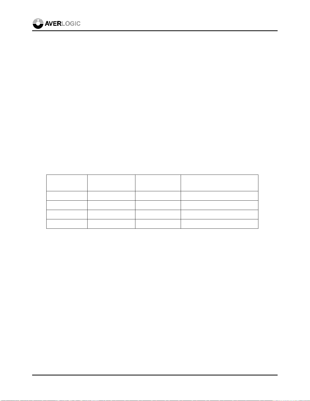
and REFVTOTAL (Reg. #42h) registers. If the XIN frequency is 14.31818 MHz and the expected
vertical frame rate is 60 Hz, the following table shows the register values for some typical resolutions.
REFHTOTAL
(Reg. #41h)
REFVTOTAL
(Reg. #42h)
Remarks
640x480 450 520 14.3MHz =: 450 x 520 x 60
800x600 376 632 14.3MHz =: 376 x 632 x 60
1024x768 296 800 14.3MHz =: 296 x 800 x 60
1280x1024 216 1072 14.3MHz =: 216 x 1072 x 60
To detect if there is input signal, turn on VSYNCIrq by writing “10” to register #40h<1:0>. “1”
status of register #65h<1> indicates that input VSYNC is detected. Reset register #40h as “00h”
before next input VSYNC detection is needed. When input VSYNC is missing, turn on the internal
timing as mentioned above.
If input VSYNC is detected but the mode is not supported by the firmware (such as out-of-spec
resolution), also turn on the internal timing to avoid sync conflict. In addition, set register #43h<6> as
1and write 00h to “color 3” registers (#B9h~BBh) to blank the input graphics/video. Turn on the
OSD to show warning signals (such as “out of sync”).
To detect if “out of sync” status is changed, turn on LineRateIrq by writing “01” to register
#40h<1:0>. “1” status of register #65h<0> indicates that input mode is changed. The firmware
should then perform mode detection. If a valid input mode is detected, turn off the internal timing.
Other control algorithm is also available.
November 28, 2001 19

AL300
6.8 Zoom Engine
The AL300 has two independent horizontal and vertical scale engines performing proprietary scaling
operations. The range of linear scaling can be from 1 up to 8 times.
The horizontal interpolation coefficient is generated by the 11-bit HRATIO (Reg. #14h and #15h),
which defines the scaling ratio with the 3 MSB as the integer part and the 8 LSB as the mantissa part.
The HRATIO is derived from the size of the displayed input video and the actual scaled display size.
The related registers include CAPHSTART (Reg. #20h and #21h), CAPHEND (Reg. #22h),
DSPHDESTART (Reg. #33h), and DSPHDEEND (Reg. #34h). The initial value for the interpolation
coefficient generator is defined by HINITPHASE (Reg. #18h).
The vertical interpolation coefficient generator, the 15-bit VRATIO (Reg. #16h and #17h) defines the
scaling ratio with the 3 MSB being the integer part and the 12 LSB being the mantissa part. The
VRATIO is derived from the size of the displayed input video and the actual scaled display size. The
registers involved include CAPVSTART (Reg. #24h and #25h), CAPVEND (Reg. #26h and #27h),
DSPVDESTART (Reg. #37h and #38h), and DSPVDEEND (Reg. #39h and #3Ah). The initial value
for the interpolation coefficient generator is defined by VINITPHASE (Reg. #1Ah). All of these
registers can be used to achieve optimum sharpness and smoothness results for different scaling ratios.
6.9 Operating Modes
The AL300 operates in three different modes: non-interlaced zoom mode, de-interlaced zoom mode,
and bypass mode
6.9.1 Non-interlaced Zoom Mode
Non-interlaced zoom mode is for synchronizing the output display with the non-interlaced input video
with a zooming ratio of larger than or equal to one. The output video can have the same or higher
resolution than the input video. First of all, the output timing parameters are decided depending on
the size of the display device. Secondly, the firmware determines what area of picture needs to be
displayed with the help of internal scan rate and position detection circuits. The input timing
parameters are set accordingly. The next step is to set the parameters of the scaling engine by the
ratio between the output video and input video. Details about programming the related registers can
be found in the Register Definition section.
6.9.2 De-interlaced Zoom Mode
De-interlaced zoom mode is different from Non-interlaced zoom mode in that the input video is
interlaced and needs to be de-interlaced. Some parameters need to be treated differently for different
operations required in odd and even fields in interlaced modes compared to non-interlaced modes.
Details about programming the related registers can be found in the Register Definition section.
November 28, 2001 20
 Loading...