

Autonics D5Y SERIES, D5W SERIES Instruction Manual
DRW171159AA
DISPLAY UNIT
D5Y/D5W SERIES
I N S T R U C T I O N M A N U A L
D5Y D5W
11111
■
DISPLAY
UNIT
~111111
" - -
" D5W M
-·
Thank you very much for selecting Autonics products.
For your safety, please read the following before using.
Safety Consideraitons
※
Please observe all safety considerations for safe and proper product operation to avoid hazards.
※
Safety considerations are categorized as follows.
Warning Failure to follow these instruc ions may result in serious injury or death.
Caution
※
1. Fail-safe device must be installed when using the unit with machinery that may cause serious injury
or substantial economic loss. (e.g. nuclear power control, medical equipment, ships, vehicles,
railways, aircraft, combustion apparatus, safety equipment, crime/disaster prevention devices, etc.)
Failure to follow this instruction may result in fire, personal injury, or economic loss.
2. Install on a device panel to use.
Failure to follow this instruction may result in electric shock or fire.
3. Do not connect, repair, or inspect the unit while connected to a power source.
Failure to follow this instruction may result in electric shock or fire.
4. Check 'Connections' before wiring.
Failure to follow this instruction may result in fire.
5. Do not disassemble or modify the unit.
Failure to follow this instruction may result in electric shock or fire.
1. When connecting the power input of D5W-MX, use AWG 24(0.20mm
over and tighten the terminal screw with a tightening torque of 0.98 to 1.18N.m.
Failure to follow this instruction may result in fire or malfunction due to contact failure.
2. Use the unit within the rated specifications.
Failure to follow this instruction may result in fire or product damage.
3. Use dry cloth to clean the unit, and do not use water or organic solvent.
Failure to follow this instruction may result in electric shock or fire.
4. Do not use the unit in the place where flammable/explosive/corrosive gas, humidity, direct sunlight,
radiant heat, vibration, impact, or salinity may be present.
Failure to follow this instruction may result in fire or explosion.
5. Keep metal chip, dust, and wire residue from flowing into the unit.
Failure to follow this instruction may result in fire or product damage.
Model
Model Display digit Size Input Power supply
D5Y-M
D5W-M
D5W-MX 110/220VAC 50/60Hz
1: AC power is only for D5W and it is optional.
※
Dimensions
D5Y-M
D5W-M/D5W-MX
Hirose connector pin header model: HIF3BA-26PA-2.54DS
※
Hirose connector socket is not included with this unit. Contact hirose connector
※
vendors for socket and cable.[Socket: HIF3BA-26D-2.54R]
"" mark indicates pin no.1 of hirose connector.
※
Case Detachment
D5Y-M D5Y-M
Be careful in order not to be wounded.
※
Please turn off the power before detaching the case.
※
※
The above specications are subject to change and some models may be discontinued without notice.
※
Be sure to follow cautions written in the instruction manual and the technical descriptions
(catalog, homepage).
Failure to follow these instructions may result in personal injury or product damage.
The symbols used on the product and instruction manual represent the following
symbol represents caution due to special circumstances in which hazards may occur.
Warning
Caution
99999
(5 digit)
85 91
72
98
96
Widen the both inside of lock devices with a driver, and push
the terminal block to the direction of front part.
DIN W72×H36mm
DIN W96×H48mm
7
36
12
48
When it is AC power option,
※
it is AC power terminal block.
Push the
terminal
block to
front part
80
90
99.5
Static, Dynamic,
4/5 Bit serial,
Serial(16/20/25 Bit)
2
) to AWG 15(1.65mm2) cable or
12-24VDC
Panel cut-out
30
Min. 40
Hirose connector
Panel cut-out
Min. 112
45
Min. 50
Hirose connector
Push the lock part on the side to the direction ①,
and then push the terminal block to the direction
to detach the case.
Min. 91
※
0.5
67
0
(Unit: mm)
67
(Unit: mm)
1
0.5
0
Specifications
Model D5Y-M D5W-M D5W-MX
Power supply 12-24VDC 110/220VAC 50/60Hz
Allowable voltage range 90 to 110% of rated voltage
Current consumption 1.1W 2VA
Size DIN W72×H36mm DIN W96×H48mm
Display method 7Segment LED Display
Display digit 4 digit(or
Max. response CLOCK 100Hz to 5kHz(Except for Static input type)
Input level High: 5V-24VDC , Low: 0-1.2VDC
Input logic Positive logic (PNP), Negative logic (NPN)
Input Static, Dynamic, 4/5 Bit serial, Serial(16/20/25 Bit)
Insulation resistance 100MΩ(at 500VDC megger)
Dielectric strength 2000VAC 50/60Hz for 1 minute
Noise resistance ±1kV the square wave noise(pulse width: 1㎲) by the noise simulator
Mechanical 0.75mm amplitude at frequency of 10 to 55Hz(for 1 min.) in each of X, Y, Z directions for 1 hour
Vibration
Malfunction
Mechanical 300m/s²(Approx. 30G) in X, Y, Z directions for 3 times
Shock
Malfunction 100m/s²(Approx. 10G) in X, Y, Z directions for 3 times
Ambient temperature
Environ
-ment
Ambient humidity 35 to 85%RH, Storage: 35 to 85%RH
Unit weight Approx. 75g Approx. 165g Approx. 267g
Environment resistance is rated at no freezing or condensation.
※
1
4
digit including sign bit), 5 digit
2
0.5mm amplitude at frequency of 10 to 55Hz(for 1 min.) in each of X, Y, Z directions for 10 minutes
-10 to 50℃, Storage: -25 to 65
℃
Connections
Static input
MINUS
25 23 21 19 17 15 13 1110987654321
26 24 22 20 18 16 14 12
12-24VDC
4/5 Bit serial input
MINUS
25 23 21 19 17 15 13 1110987654321
26 24 22 20 18 16 14 12
12-24VDC
Power terminal for AC power option of D5W series
※
Above terminal connection diagrams's number set by pin no.1 of hirose connector. Please note that "
※
indicates pin no.1 of hirose connector.
Input Circuit
Positive logic(PNP) Negative logic(NPN)
0.5
0
31
Input Timing
0.5
0
Parallel input
Positive logic(PNP)
45 5
Input
DATA
LATCH
Serial input
Positive logic(PNP) : CLOCK max. 5kHz
LATCH
①
CLOCK
②
DATA
Negative logic(NPN) : CLOCK max. 5kHz
LATCH
CLOCK
②
DATA
DP
3
101C
10
+5VNC
10
+5V DNC
1 2 3 4 5 6 7 8
Use teminals of size specied below.
<Forked>
___r-
SIGNAL DISPLAY
t1 t2Pwt3
~II~
-----c:::::x=::))
ABCDABCDABCDA
10310210110
2
D10
DP
DP
3101
2
10
DP
b
a
InputPNP :
22k
22k
0.2ms
C1 C2 C3
1 2 3 N-2 N-1 N 1 2
DOT C A
LATCH
CLOCK
220V 110V 0V
SOURCE
a b
Min.
Max.
3.5mm
7.0mm
22k
22k
Negative logic(NPN)
Input
DATA
LATCH
BCD
INPUT
Input level
※
• High: 5-24VDC
• Low: 0-1.2VDC
CN-2 CN-1
• • • •
~
______
0.2ms
C1 C2 C3
1 2 3 N-2 N-1 N 1 2
CN-2 CN-1
Dynamic input
MINUS
25 23 21 19 17 15 13 1110987654321
0
26 24 22 20 18 16 14 12
12-24VDC
B
Serial input
MINUS
25 23 21 19 17 15 13 1110987654321
26 24 22 20 18 16 14 12
B
12-24VDC
In case of static input, 5 digit cannot be used because of
※
external terminal.
To display 5 digit in dynamic, 4/5 bit serial, serial input,
※
display range is 0 to 99999 and it cannot display minus
sign. Therefore, the applied signal to the external MINUS
sign input terminal (pin no.21) is ignored.
Regardless of input logic, connect external DP terminal (pin
※
no.17, 18, 19) or external MINUS sign input terminal (pin
no.21) to +5V (pin no.20) and it displays decimal point and
minus sign.
t1Pwt2 t3
DP
3
1
10
10
2
+5VNC
10
DP
DP
1
10310
2
10
DP
SIGNAL DISPLAY
Pw=t1+t2+t3
※
• Pw: Min. 0.2ms
• t1: Min. 0.05ms →Data latch
• t2: Min. 0.1ms →Data shift
• t3: Min. 0.05ms →Data latch
tw
TT
-'
ta b
CN C1 C2
tw
TT
ta b
CN C1 C2
3
10
101DOT C A
LATCH
10 102100D B
DATA NC
LATCH CLOCK+5VNC
InputNPN :
5V
22k
22k
ta: Min. 0.05ms
tw: Min. 0.02ms
{
tb: Min. 0.03ms
ta: Min. 0.05ms
tw: Min. 0.02ms
{
tb: Min. 0.03ms
22k
22k
BCD
INPUT
" mark
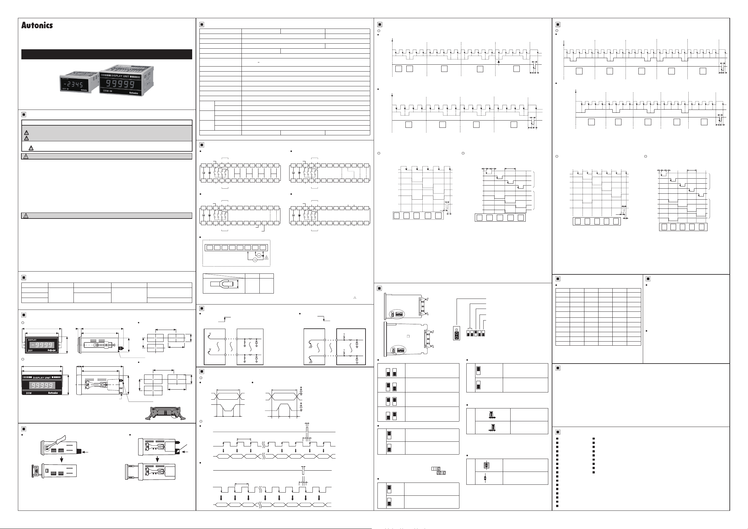
Time Chart (4-digit)
Serial input(Serial connection)
20 Bit DATA input example(Negative logic)
Start
1 2 3 4 5 6 7 8 9 10 11 12 13 14 15 16 17 18 19 20 1
Input chart
DOT
CLOCK
DATA
LATCH
DISPLAY
※
※
※
16 Bit DATA input example(Negative logic)
Input chart
DISPLAY
※
※
※
※
Inner selection switch: SW1 → ON, SW2 → ON, SW3 → OFF,
DISPLAY
※
※
In case of positive logic, it will be reversed.
※
※
※
- 4 3
ta: Min. 0.05ms, tw: Min. 0.02ms, tb: Min. 0.03ms
The above waveform is for negative logic input. In case of positive logic, it will be reversed.
When DOT signal data(16th) is input on 100 position, minus sign is indicated.
CLOCK
DATA
LATCH
ta: Min. 0.05ms, tw: Min. 0.02ms, tb: Min. 0.03ms
The above waveform is for negative logic input. In case of positive logic, it will be reversed.
DATA is xed when CLOCK is changed from high to low and held when LATCH is changed from high to low.
DATA hold term is before next LATCH is changed from high to low.
4/5 Bit serial input(Serial connection) Dynamic input(Parallel connection)
CLOCK
LATCH
ta: Min. 0.05ms, tw: Min. 0.02ms, tb: Min. 0.03ms
The above waveform is for negative logic input.
If DOT signal is inputted on 10
terminal, it displays minus sign.
(Inner selection switch SW4 →ON)
Using external DP terminal and MINUS terminal, it
displays decimal point and minus sign.
(Inner selection switch SW4 →OFF)
The above example of DISPLAY is for non-using zero
blanking function. If using zero blanking function, the "0"
of 103 position is not displayed.
(Inner selection switch SW3 →ON)
10
Start
1 5 9 132 6 10 143 7 11 154 8 12 16 1
D
4 3
10
SW4 → ON, SW5 → OFF
~
A
B
C
D
i i ! i i i
DOT
. . : .
- 0 2. 4 8
ID
□□'□
3102101100
10
10
DOT DOT DOT DOTD
3
3
0
position by external DOT
D D DC C C CB B B BA A A A
Minus
2.
2
10
D D D DC C C CB B B BA A A A
10
sign is
1
indicated
2
2
10
tw
,.,.,...
ta
tb
□
fl
1
10
Inner selection switch: SW1 → ON, SW2 → ON, SW3 → OFF,
DISPLAY
Pw: Min. 0.2ms, t1: Min. 0.05ms, t2: Min. 0.10ms, t3: Min. 0.05ms
※
The above waveform is for negative logic input. In case of positive
※
logic, it will be reversed.
For 4 digit, external 104 LATCH input terminal is not available.
※
If DOT siganl is inputted on 100 position by external DOT terminal,
※
it displays minus sign.(Inner selection switch SW4 →ON)
Using external DP terminal and MINUS terminal, it displays
※
decimal point and minus sign.(Inner selection switch SW4 →OFF)
LATCH input should be later than BCD input, otherwise, it wll
※
display the previous data.
The above example of DISPLAY is for non-using zero blanking
※
function. If using zero blanking function, the "0" of 103 position is
not displayed. (Inner selection switch SW3 →ON)
SW4 → ON, SW5 → OFF
t1 t2 t3 Pw
~
3
10
2
10
1
10
0
~]
10
A
: : : : :
B
C
~
D
. : . : .
DOT
- 0 2 4. 8
ID
□'□
3102101100
10 10
1
0
10
1
0
10
~
0'01
Inner selection switch
Input logic
D5Y-M
Positive
logic
D5W-M
Input mode
SW1 SW2
ON
ON
OFF
SW1 SW2
ON
OFF
SW1 SW2
ON
OFF
SW1 SW2
ON
OFF
Zero blanking function
SW3
I
I~
Zero blanking function
※
It is to remove "0" indication which is no meaning.
EX)When data value is "10"(4 digit)
• Zero blanking function is applied :
• Zero blanking function is not applied :
Minus sign/DOT(Decimal point) input terminal
SW4
I
I~
Static input
OFF
ON
Dynamic input
OFF
ON
4/5 Bit serial input
OFF
ON
Serial input
OFF
ON
Use zero blanking function
OFF
ON
Non-using zero blanking function
OFF
I
ON
Using DOT terminal(pin no. 5)
OFF
ON
Using external DP(pin no. 17, 18, 19, 20)
terminal and minus(pin no. 21) terminal
OFF
I
Negative
logic
m.-
1 2 3 4 5
Factory default: SW1→OFF, SW2→OFF, SW3→ON, SW4→OFF,
※
.
Display digit
SW5
Ii~
※
.
Input logic
SW6
I
lffll
※
.
LATCH input signal
SW7
I
II
※
Input mode
Zero blanking function
Minus sign/DOT(Decimal point)
input terminal
Display digit
ON
OFF
SW5→OFF, SW6→Negative logic, SW7→OFF
ON
OFF
ON
OFF
In case of static input, 5 digit cannot be used because of
external terminal.
Positive
logic
Positive
logic
If changing inner selecting switch when power is ON,
it does not operate as a changed mode. If the mode is
changed when power is ON, please turn OFF and then
turn ON the power.
~
BCD output and latch signal of low speed serial output, which are
option output of Autonics' pulse meter
(MP5Y/W Series) and panel meter(MT4Y/W Series) is output to
positive logic(PNP). If connecting D5Y/W, use it after setting SW6
to NPN and soldering(ON) the semi-contact(SW7) of inner PCB
solder plate.
5 digit(0~99999)
4 digit(-9999~9999)
I
Negative
Positive logic(PNP) input
logic
Negative
:--------r--
ON
OFF
Negative logic(NPN) input
logic
Reverse LATCH signal to set
logic in SW6
Correspond LATCH signal to
set logic in SW6
I
tw
,m
wll
tatatb
tw
tb
LATCH
input SIG.
BCD
input SIG.
i
Time Chart (5-digit)
Serial input(Serial connection)
25 Bit DATA input example(Negative logic)
Start
Input
1 62 73 84 95 10 15 20 2514 19 2413 18 2312 17 2211 16 21 1
chart
DOT DOT DOT DOT DOT DOT
D D D D D
CLOCK
DATA
LATCH
DIS-
PLAY
20 Bit DATA input example(Negative logic)
ta: Min. 0.05ms, tw: Min. 0.02ms, tb: Min. 0.03ms
※
The above waveform is for negative logic input. In case of positive logic, it will be reversed.
※
Minus sign cannot be indicated in 5 digit type. [The input of DOT signal on 100 position and MINUS terminal(pin no. 21)
※
is ignored.]
DATA is xed when CLOCK is changed from high to low and held when LATCH is changed from high to low.
※
DATA hold term is before next LATCH is changed from high to low.
※
4/5 Bit serial input(Serial connection) Dynamic input(Parallel connection)
Inner selection switch: SW1 → ON, SW2 → ON, SW3 → OFF,
CLOCK
LATCH
DISPLAY
ta: Min. 0.05ms, tw: Min. 0.02ms, tb: Min. 0.03ms
※
The above waveform is for negative logic input.
※
In case of positive logic, it will be reversed.
Minus sign cannot be indicated in 5 digit type.
※
The above example of DISPLAY is for non-using zero
※
blanking function. If using zero blanking function, the "0" of
10
(Inner selection switch SW3 →ON)
C
8 4 2 1. 0
10 10
Start
Input
1 5 9 13 17
chart
CLOCK
DATA
LATCH
DISPLAY
A
B
C
D
DOT
position is not displayed.
2 6 10 14 18
D D D D D
C C C C C
10 10
SW4 → ON, SW5 → ON
~
~
i i ! ; ; i
~,i•:
' : : : :
0 1. 2 4 8
ID
D
3102101100
10 10
Input DATA Chart
Negative logic(NPN) input DOT (decimal point) and minus sign input is not
Display A B C D LATCH
H H H H L
0
L H H H L
1
H L H H L
2
L L H H L
3
H H L H L
4
L H L H L
5
H L L H L
6
L L L H L
7
H H H L L
8
L H H L L
9
Hold X X X X X
Above DATA chart is for negative logic (NPN). In case of positive
※
logic (PNP), DATA input levels are reversed.
Input level: High →5-24VDC, Low →0-1.2VDC
※
"X": Either high or low level can be input.
※
Cautions during Use
~
1. Follow instructions in 'Cautions during Use'.
Otherwise, t may cause unexpected accidents.
2. 12-24VDC power supply should be insulated and limited voltage/current or Class 2, SELV power supply device.
3. Install a power switch or circuit breaker in the easily accessible place for supplying or disconnecting the power.
4. Keep away from high voltage lines or power lines to prevent inductive noise.
I
In case installing power line and input signal line closely, use line filter or varistor at power line and shielded
wire at input signal line.
Do not use near the equipment which generates strong magnetic force or high frequency noise.
5. This unit may be used in the following environments.
①
Indoors (in the environment condition rated in 'Specifications')
Altitude max. 2,000m
②
Pollution degree 2
③
Installation category II
④
Major Products
I
~
Photoelectric Sensors Temperature Controllers
■ ■
Fiber Optic Sensors Temperature/Humidity Transducers
■ ■
Door Sensors SSRs/Power Controllers
■ ■
Door Side Sensors Counters
■ ■
Area Sensors Timers
■ ■
Proximity Sensors Panel Meters
■
Pressure Sensors Tachometers/Pulse (Rate) Meters
■
Rotary Encoders Display Units
■
Connector/Sockets Sensor Controllers
■
Switching Mode Power Supplies
■
Control Switches/Lamps/Buzzers
■
I
I/O Terminal Blocks & Cables
■
Stepper Motors/Drivers/Motion Controllers
■
Graphic/Logic Panels
■
Field Network Devices
■
Laser Marking System (Fiber, Co₂, Nd:YAG)
■
Laser Welding/Cutting System
■
C
3
3 7 11 15 19
4 8 12 16 20 1
B B B B B
A A A A A D
3
~
ta
~:
□'□
01
C C CB B B B BA A A A A
tw
tb
1
2
10
2
10
Inner selection switch: SW1 → ON, SW2 → OFF, SW3 → OFF,
10
10
10
10
10
DOT
DISPLAY
Pw: Min. 0.2ms, t1: Min. 0.05ms, t2: Min. 0.10ms, t3: Min. 0.05ms
※
The above waveform is for negative logic input.
※
In case of positive logic, it will be reversed.
Minus sign cannot be indicated in 5 digit type.
※
LATCH input should be later than BCD input, otherwise, it will
※
display the previous DATA.
The above example of DISPLAY is for non-using zero blanking
※
function. If using zero blanking function, the "0" of 10
not displayed.
(Inner selection switch SW3 →ON)
1
10
1
10
SW4 → ON, SW5 → ON
t1 t2 t3 Pw
3
2
1
0
A
B
C
D
0 1. 2 4 8
10 10310210110
10
10
Decimal Point
Serial input. [SW4 = OFF]
■
■
■
■
Terminal 17-20 :
DOT (decimal point) and minus sign input is
Serial input.[SW4 = ON]
When it is dynamic input and 4/5 bit input, it connects
①
with no.5 pin.(Refer to time chart (4 digit).)
When it is serial input, 1 bit of serial data should have
②
DOT and minus sign and the DATA is input.
(Refer to time chart (4 digit).)
18-20 :
19-20 :
21-20 :
OPEN :
888*8
888*8
8*888
8888
88888
DR W171159 A A
0
01248
0
0
tw
ta tb
tw
ta tb
LATCH
input SIG.
BCD
input SIG.
position is
 Loading...