

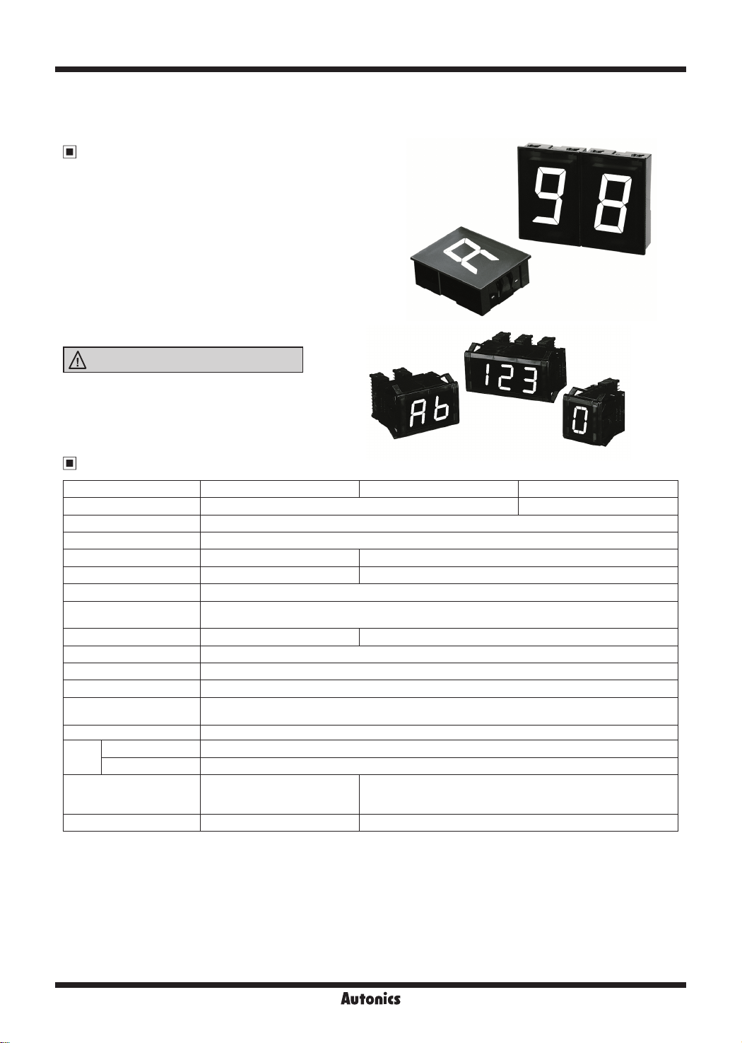
D1SC-N/D1SA Series
7-Segment Display Unit with High Bright Characters
(D1SC-N: W32×H57mm, D1SA Series: W11×H22mm)
Features
● Selectable decimal (0 to 9) or hexadecimal (0 to 9, A to F)
indication code
Selectable positive or negative input logic
Selectable serial or parallel data input method
● 7-segment, red/green display (D1SA Series)
● Power source: 12-24VDC
● Wide range on signal input voltage level
(Low: Max. 0-1.2VDC, High: 4.5-24VDC)
● Easy multi-stages connection (D1SA Series)
● Zero Blanking function
Please read “Safety Considerations”
----,---------=_I
in the instruction manual before using.
I&
D1SA Sereis
D1SC-N
Specifications
Model D1SC-N D1SA-RN D1SA-GN
Display method 7-segment LED display (red) 7-segment LED display (green)
Power supply 12-24VDC
Allowable voltage range 90 to 110% of rated voltage
Current consumption Max. 70mA Max. 35mA
Character size W32×H57mm W11×H22mm
Display character
Input
Input resistance 12
Input level High: 4.5-24VDCᜡ, Low: 0-1.2VDC
Max. Clock Max. 3kHz
Output Data output (serial input), zero blanking output
Input logic
Noise immunity ±300V the square wave noise (pulse width: 1μs) by he noise simulator
Environ
-ment
Accessory
Unit weight Approx. 100g Approx. 22g (including right/left caps)
※
1: It is option.
※
2: Only D1SC-N supports Minus displaying.
※
Max. Clock is for 1:1 of duty ratio (ON, OFF ratio).
※
Environment resistance is rated at no freezing or condensa ion.
※
2
Ambient temperature 0 to 60℃, storage: -10 to 85
Ambient humidity 35 to 85%RH
• Decimal number: 0 to 9, decimal point • Hexadecimal number: 0 to 9, A to F, decimal point
• Parallel: Parallel 4-bit data, latch, zero blanking, decimal point
• Serial: Serial 4-bit or 5-bit data, clock, zero blanking, latch, decimal point (for 4-bit input)
Selectable positive logic (PNP) or negative logic (NPN)
(D1SC-N: by the function set switch, D1SA Series: by inner soldering)
Housing[5264-10],
Terminal[5263 (PBT)],
Sub-PCB for multi-stage connection
kΩ
ᜡ
20kΩ
ᜡ
℃
Connector (CT-10S), Cap
•
※
1
R-30
Autonics
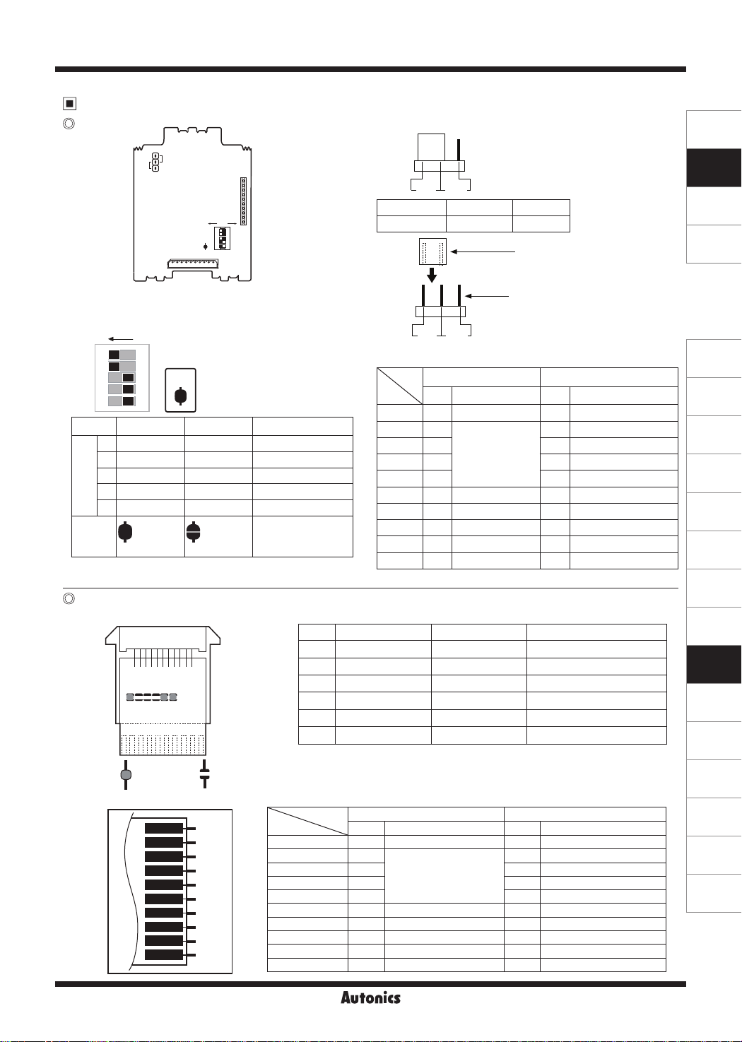
Terminal Layout and Function
(Q)
D1SC-N
①
OFF
ON
SW1
JP1
③
1
CN1
(rear terminal layout)
Function set switches (SW2, JP1)
②
ON
5
3 4
JP1
2
1
ON
Switch ON OFF Function
1 Decimal Hexadecimal Characters
2 Parallel Serial Input
SW2
3 5-bit 4-bit Serial input
4 Used Not used Serial data output
5 Used Not used Zero Blanking
JP1
※
For Parallel input, set this as OFF.
(Q)~--
D1SA Series
①
Input/Output terminals
②
7-segment Minus
1:
For Serial input, set this as ON.
----
Function set switches
①
S4 J2 J1 S3 S2 S1
②
※
ON = (short) OFF = (open)
CN2
③
ON
OFF
②
SW2
5
1
10
<factory default>
<factory default>
10
9
8
7
6
5
4
3
2
1
1
10
Minus
Terminal
1 V+ 12-24VDC VCC 12-24VDC
2 D0
3 D1 CK Clock input
4 D2 DI Data input
5 D3 DO Data output
6 BI Zero Blanking input BI Zero Blanking input
7 BO Zero Blanking output BO Zero Blanking output
8 LE LATCH input LE LATCH input
9 DP Point input DP Point input
10 GND 0V GND 0V
7-Segment Display Unit
Function set jumper (SW1)
①
~
ON
OFF
<factory default>
ON OFF Function
1=-=-t=1
Neg. logic (NPN) Pos. logic (PNP)
--------r===o¼-·
=II
Input logic
____r_
Jumper
-
- I
...
Jumper pin
~
ON
OFF
Input/Output terminals
③
Input
Terminal
1 V+ 12-24VDC VCC 12-24VDC
2 D0
3 D1 CK Clock input
4 D2 DI Data input
※
Switch ON OFF Function
S1
S2 Parallel Serial Input
S3 5-bit 4-bit
J1 Used Not used
J2 Used Not used Zero Blanking
S4 Neg. logic (NPN) Pos. logic (PNP) Input logic
※
1:
For serial input, set this as ON. For Parallel input, set this as OFF.
Input
5 D3 DO Data output
1
6 BI Zero blanking input BI Zero blanking input
7 BO
8 LE Latch input LE Latch input
9 DP Decimal point input DP Decimal point input
10 GND 0V GND 0V
※
L__
Decimal Hexadecimal Characters
Parallel input Serial input
Code Function Code Function
Parallel input Serial input
Code Function Code Function
N·C
Do not connect anything
Data input
Zero blanking output
Terminals of CN1 and CN2 is corresponding 1:1.
Data input
BO Zero blanking output
Serial input
Serial data output
N·C Do not connect any hing
SENSORS
CONTROLLERS
MOTION DEVICES
SOFTWARE
(J)
Temperature
Controllers
(K)
SSRs
(L)
Power
Controllers
(M)
Counters
(N)
Timers
(O)
Digital
Panel Meters
(P)
Indicators
(Q)
Converters
(R)
Digital
Display Units
※
1
(S)
Sensor
Controllers
(T)
Switching
Mode Power
Supplies
(U)
Recorders
(V)
HMIs
(W)
Panel PC
(X)
Field Network
Devices
R-31
D1SC-N/D1SA Series
Block Diagram
Parallel input
Power
[
Data
input
LATCH - LE
Decimal point -DP
Zero blanking input - BI
Zero blanking output - BO
Serial input
Power
[
CLOCK - CK
Data input - DI
LATCH - LE
Decimal point - DP
Data output - DO
V+
GND
D0
D1
D2
D3
V+
GND
Stable
power
Input circuit
Stable
power
Input
circuit
Input
circuit
DECODER
DRIVER
Zero blanking
control circuit
DECODER
DRIVER
Zero blanking input - BI
Zero blanking output - BO
Dimensions
D1SC-N
72
32
10°
Accessories
OFF
ON
SW1
CN2
CN1
Header
Input circuit
※
pin is not used.
The ②
2.3 25.7
Tl
57
96
CN1: Connector specification
■
● Connector maker: Korea Morex
• Housing: 5264-10
• Header: 5264-10A (straight)
• Terminal: 5263 (PBT)
● Using cable specification
• AWG28 to 22 (cable diameter: Max. Ø1.9mm)
• Shielding length of wire cover: 2.4 to 2.9mm
Housing[5264-10] Terminal[5263 (PBT)]
Zero blanking
control circuit
90
● Panel cut-out
72×N-3.5
■ CN2: Connector for multi-stage
● This connector must be used with
connection PCB
● CN1 and CN2 must be connected as
below drawing.
※
N: Number of units
※
Panel thickness: 2 to 4mm
90.5
8mm
r--------,
c:::::::@C:J
c:::::::@C:J
c:::::::@C:J
c:::::::@C:J
c:::::::@C:J
c:::::::@C:J
c:::::::@C:J
c:::::::@C:J
c:::::::@C:J
c:::::::@C:J
Multi-stage connector
(unit: mm)
27mm
R-32
Autonics

7-Segment Display Unit
D1SA Series
11
(Q) (Q)
Accessory Sold separately
● Connector (model: CT-10S)
I I I I I II _
A
54
35
19
13.5
7.5
11
ff]
42
37
22
7.5
3.5
2-Ø3.4
6
----r----r---
7.5
32
● Panel cut-out
33
__
,_
___
● Panel cut-out chart
Digit (N) A (20×N+12) B (20×N+10)
1 32 30±0.1
2 52 50±0.1
3 72 70±0.1
4 92 90±0.1
5 112 110±0.1
6 132 130±0.1
7 152 150±0.1
8 172 170±0.1
● CAP
● D1SA-RN: DAR(L) -R (left/right 1 set)
● D1SA-GN: DAR(L) -BL (left/right 1 set)
※
23
Cap is optional (1set).
(unit: mm)
SENSORS
31
Ill
B
,
CONTROLLERS
MOTION DEVICES
SOFTWARE
(J)
Temperature
Controllers
(K)
SSRs
(L)
Power
Controllers
(M)
Counters
(N)
Timers
Input Data Chart
Indication Negative input Positive input
※
1
Minus
Hexa
decimal
Blank Blank
Blank Blank
Decimal
- -
- - 3 3
- -
- -
- -
Blank Blank
- -
- -
-
-
Blank Blank
-
-
-
Blank Blank L H L H H L H L
Blank Blank L H L L H L H H
Blank Blank L L H L H H L H
Blank Blank L L L H H H H L
Blank Blank L L L L H H H H
7-segment
Hexa
decimal
n n
u u
I I
I I
Decimal
2 2
I..{
I..{
5 5
E, E,
, ,
I I
B B
g g
R
b
r
L
d
E
F
Blank L L H H H H L L
D3 D2 D1 D0 D3 D2 D1 D0
H H H H L L L L
H H H L L L L H
H H L H L L H L
H H L L L L H H
H L H H L H L L
H L H L L H L H
H L L H L H H L
H L L L L H H H
L H H H H L L L
L H H L H L L H
※
When BI terminal connect GND, “0” is
displayed. When BI terminal is open, it is
blank (not display)
※
"X": Either high or low level can be input.
※
1: Only D1SC-N supports Minus display.
Set the rear JP1 as OFF.
※
Blank: If input signal as input DATA, it does
not display.
(O)
Digital
Panel Meters
(P)
Indicators
(Q)
Converters
(R)
Digital
Display Units
(S)
Sensor
Controllers
(T)
Switching
Mode Power
Supplies
(U)
Recorders
(V)
HMIs
(W)
Panel PC
(X)
Field Network
Devices
Autonics
R-33

D1SC-N/D1SA Series
Input Circuit
D1SC-N
● Positive logic (PNP) input (SW1: OFF)
10kΩ
Input
12kΩ
-
※
Input level - High: 4.5-24VDC, Low: 0-1 2VDC
(Q)
D1SA Series
● Positive logic (PNP) input (SW1: OFF)
100
※
Input level
kΩ
Input
20
kΩ
Data Input Method
20kΩ
I
IC
High: 4.5-24VDC
Low: 0-1.2VDC
● Negative logic (NPN) input (SW1: ON)
+5V
IC
Input
● Negative logic (NPN) input (SW1: ON)
Input
20
12kΩ
kΩ
10kΩ
5V
-
100
kΩ
I
20kΩ
IC
IC
Parallel input
● 4-bit static parallel input (e.g.: displays ABCD.)
3
2
1
0
10
10
4-bit Data3+Point3
4-bit Data2+Point2
4-bit Data1+Point1
4-bit Data0+Point0
LATCH
● 4-bit dynamic parallel input (e.g.: displays ACE007.)
10
...
[BJ
1
[BJ
4-bit Data
Point
LATCH 5
LATCH 4
LATCH 1
LATCH 0
5
10
[BJ
[BJ
10
10
10
0
10
LATCH 5
LATCH 4
LATCH 3
LATCH 2
LATCH 1
LATCH 0
4-bit Data3+Point3
4-bit Data2+Point2
4-bit Data1+Point1
4-bit Data0+Point0
LATCH
::x====:::x
x=::::=:x
x=::::=:x
_x=::::=:x~:
HLHL+L
HLHH+L
HHLL+L
HHLH+H
. ' ' .
[BHBJ
3
2
10
10
Pw
4-bit
HLHL HHLL HHHL LLLL LLLL LHHH
Data
Point
: : : : :
t1 t3
~
----,--:
-----,--:
[BJ
t2
i : i i !
i i : : :
-----;:----,------.
______,__,
----,.-------,-i ~ : i
• t • • t
[BJ
[HJ
5
10
10
10
[BJ
3
~
[B
HHJ
1
0
10
10
※
Clock: Max. 3kHz
: : :
[BJ
[El]
0
1
2
10
※
Pw=t1+t2+t3
Pw: 0 33ms (Min.)
t1: 0.05ms (Min.) → Data LATCH
t2: 0.23ms (Min.) → Data move
t3: 0.05ms (Min.) → Data
10
10
R-34
Autonics

R-35
s,1uo1ny
Devices
Field Network
(X)
Panel PC
(W)
HMIs
(V)
Recorders
(U)
Supplies
Mode Power
Switching
(T)
Controllers
Sensor
(S)
Display Units
Digital
(R)
Converters
(Q)
Indicators
(P)
Panel Meters
Digital
(O)
Timers
(N)
Counters
(M)
Controllers
Power
(L)
SSRs
(K)
I
ooooooooooJ
10
GND
BO
V+
✓
LATCH
'
✓
)---
✓
input
Data
-
GND
:::
DP
LE
BO
-
BI
;:: ;::
(over 5-digit)
From next digit
{~
o-
:?--
1
-
D0
D1
D2
D3
DP
D3
D2
D1
D0
V+
CN2
10
3
I
1 10
LSB (0)
CN1
tttttttttttttttttttt
w
-.1-----J.--
tw
I
0000000000
10
GND
DP
LE
....._
BO
BI
D3
D2
D1
D0
V+
CN2
10
1
1
Data Data Data
0.33ms
MSB (2)
J I
1 10
Point
10
2
I
0000000000
10
'-:-
GND
;::
DP
;::
LE
-
BO
:::
I! I!
~ ~ ~
D0
D----
D1
c::::::>-----
D2
c::::::>----
D3
DP
I
BI
D3
.....__
D2
,___ ,___
D1
...._ ...._
D0
V+
1
CN2
[BJ
Point
LSB (1)
MSB (0)
a
ta
tw: 0 05ms (Min.)
ta: 0 23ms (Min.)
CN1
J
1 10
~
:::
10
:::
I~
1
D0
c::::::>-- c::::::>--
D1
c::::::>----- c::::::>-----
D2
c::::::>----
D3
DP
[BJ [BJ [BJ
Point
LSB (2)
MSB (1)
CN1
I
I
c::::::>----
LSB (3P)
D1 D1 D1 D1
D0 D0 D0 D0
'-:-
:::
10
;::
1
D0
D1
D2
D3
DP
0000000000
10
GND
DP
LE
....._
BO
BI
D3
.....__
D2
,__
D1
...--
D0
V+
CN2
MSB (3)
Data
D3 D3 D3 D3D4 D4 D4 D4
D2 D2 D2 D2
10
0
Point
L L L L L L L L L L L L L LH H H H H H
SHIFT
t
START
CN1
J
1 10
● Static parallel input (zero blanking method)
When not using Zero Blanking, connect BI terminal to GND.
※
CN1, CN2 terminals of D1SC-N corresponds 1:1 and it is able to connect as CN1 depending on the need.
※
The below connection is example of D1SC-N. For D1SA, connection is same but the order of pin is reverse.
※
Parallel input: 4-digit
@
Do wiring after removing the rear case of the product.
※
Multi-Stage Connection Method
~
1-bit data
CLOCK
LATCH
● 5-bit seriaI input (e.g.: displays A25.0)
Controllers
Temperature
(J)
SOFTWARE
MOTION DEVICES
CONTROLLERS
SENSORS
iOl
[BJ
_+ _+
LSB (0)
LSB (1)
MSB (0)
2
[HJ
※
LSB (2)
MSB (1)
[HJ
_+
D1 D1 D1D0
D0 D0 D0
H H
Data Data Data
1
※
LQJ
_+
LSB (3P)
MSB (2)
D3 D3 D3D2
D2 D2 D2D1
MSB (3)
Data
D3
L L L L L L L L L L L L L
H
tttttttttttttttt
SHIFT
t
-.1-----J.--
ta
tw
tw: 0.05ms (Min.)
ta: 0.23ms (Min.)
0 33ms
In case of positive logic (PNP), hexadecimal number
※
Clock max. 3kHz
※
In case of negative logic (NPN), connect DP to GND.
2: In case of 4-bit Serial input, to display decimal point, connect DP of the rear input terminal to V+.
※
1: To display Minus, set the rear JP1 as OFF.
※
1-bit data
CLOCK
LATCH
START
● 4-bit serial input (e.g.: displays -20.8)
Serial input
@
7-Segment Display Unit

D1SC-N/D1SA Series
● Dynamic parallel input (zero blanking method)
1 10
(
0000000000
CN1
CN2
1
-
V+
D0
::
;'.
D1
D2
D3
-
::
BI
BO
--0
LE
--Q
DP
GND
0
10
-
..::.
10
I
I
I
1 10
(
CN1
0000000000
1
10
CN2
1
-
V+
D0
::
;'.
D1
D2
D3
- -
:: ::
BI
BO
--0
LE
-;?
DP
GND
..::. ..::. ..::.
10
I (
1 10
CN1
I
0000000000
2
10
CN2
V+
D0
D1
D2
D3
BI
BO
LE
-~
DP
GND
1
-
::
';'.
::
10
I
Serial input: 4-digit
● Serial input (zero blanking method)
CN2
1
VCC
-=-
0
CK
~
DI
--g
DO
BI
::
BO
--§
LE
..::.
I
I
I
CN1
1 10
(0000000000
DP
--0
GND
1 10 1 10 1 10
(0000000000
CN1
0
10
CN2
1
VCC
-=- -=-
0 0 0
CK
;'. ;'.
DI
DO
I
10
~
:: ::
BI
BO
--§
LE
~ ~
DP
--Q
GND
..::. ..::.
I
1
(0000000000
CN1 CN1
CN2
1
VCC
CK
DI
DO
I
I
-
BI
::
BO
:: ::
LE
DP
--0
GND
I
2
10
1 10
(0000000000
CN1
I
I
(0000000000
10
r-c=J
I
-;?
3
10
-
-
GND
3
VCC
CN2
CN2
DO
BO
GND
CK
LE
DP
LATCH 0
LATCH 1
LATCH 2
LATCH 3
V+
D0
D1
D2
D3
BI
BO
LE
DP
-
DI
BI
~
::
fO
-
10101010
I
-=-
::
::::
-
::
::
::
10
I
1
1
-
V
=
D0
~
D1
)==:a
D2
'-
D3
BO
·······C
From next digit
(over 5-digit)
DP
~
GND
-
DI
Data input
-
VCC
-
-
CK
From next digit
(over 5-digit)
BO
······c:::J
LATCH
GND
-
Zero Blanking Method?
It is to remove "0" indication which is no meaning.
E.g.1) When displaying 10
①
Using Zero Blanking
I I
11101
3
※
If indication data is "101", meaningful tens place "0" will be displayed.
10010110210
Using zero blanking for multi-stage
Set 5 (zero blanking output) of the rear function set switch (SW2) as ON.
For 10 (0) to display '0', set this as OFF.
1) Using Zero Blanking
I I I
2) Not using Zero Blanking
10101
3
("0" of 10
, 102 are no meaning
and they are not displayed.)
V+
1101
0101102103
10
BI
~=H
,101
0101102103
10
BI
D
GND
② Not using Zero Blanking
101011101
3
BI BI BIBO BO BO BO
3
10
11
3
10
10
BI BIBO BO BO
10
10010110210
2
11
11
2
1
lrD
10
10
GND
BI BO
lrD
1
GND
0
10
0
10
R-36
Autonics

SENSORS
CONTROLLERS
MOTION DEVICES
SOFTWARE
(J)
Temperature
Controllers
(K)
SSRs
(L)
Power
I I
Controllers
(M)
Counters
(N)
Timers
(O)
Digital
Panel Meters
(P)
Indicators
(Q)
Converters
(R)
Digital
Display Units
(S)
Sensor
Controllers
(T)
Switching
Mode Power
Supplies
(U)
Recorders
(V)
HMIs
(W)
Panel PC
(X)
Field Network
11
I I I
Devices
R-37
Shift register
I I I I I I I I I I I I I I
[ SET S00.01 ]
[ SET S00.02 ]
[ SET S00.03 ]
[ SET S00.04 ]
[ SET S00.05 ]
7-Segment Display Unit
[ SET S00.06 ]
[ SET S00.07 ]
[ SET S00.08 ]
[ SET S00.09 ]
Reset
[ SET S00.00 ]
( M000 )
(M001)
CLOCK output
(P010)
HEX "A" value
HEX "A" value
data output
Transmission order
to M01
(P011)
( MOV h000A M01 )
M013
"A" display
M012
LATCH Output
n
(P012)
[ END ]
1111
V
·a
.e
ii
M011
M010
□
The Application of PLC Program [Serial Input Type]
~
Connection method: Refer to serial connection type when using more than 2.
1. Display Unit D1SA-
2. Data input type: Serial
3.
M001
M001
P000
M000
M000
M001
4. Display result: "A" Display
5. PLC: LSIS (LS Industrial Systems), MASTER-K Series
6. When using serial type, use transistor output card of PLC
7. Negative logic (NPN)
M000
M000
M001
M000
I
S00.09
S00.01
S00.03
S00.05
S00.07
S00.09
S00.02
S00.04
S00.06
S00.08
S00.02
S00.04
S00.06
S00.08
hhhh
P000
S00.01
S00.03
S00.05
S00.02
S00.04
S00.06
S00.07
S00.08
S00.09
 Loading...