

DR W17115 8 A A
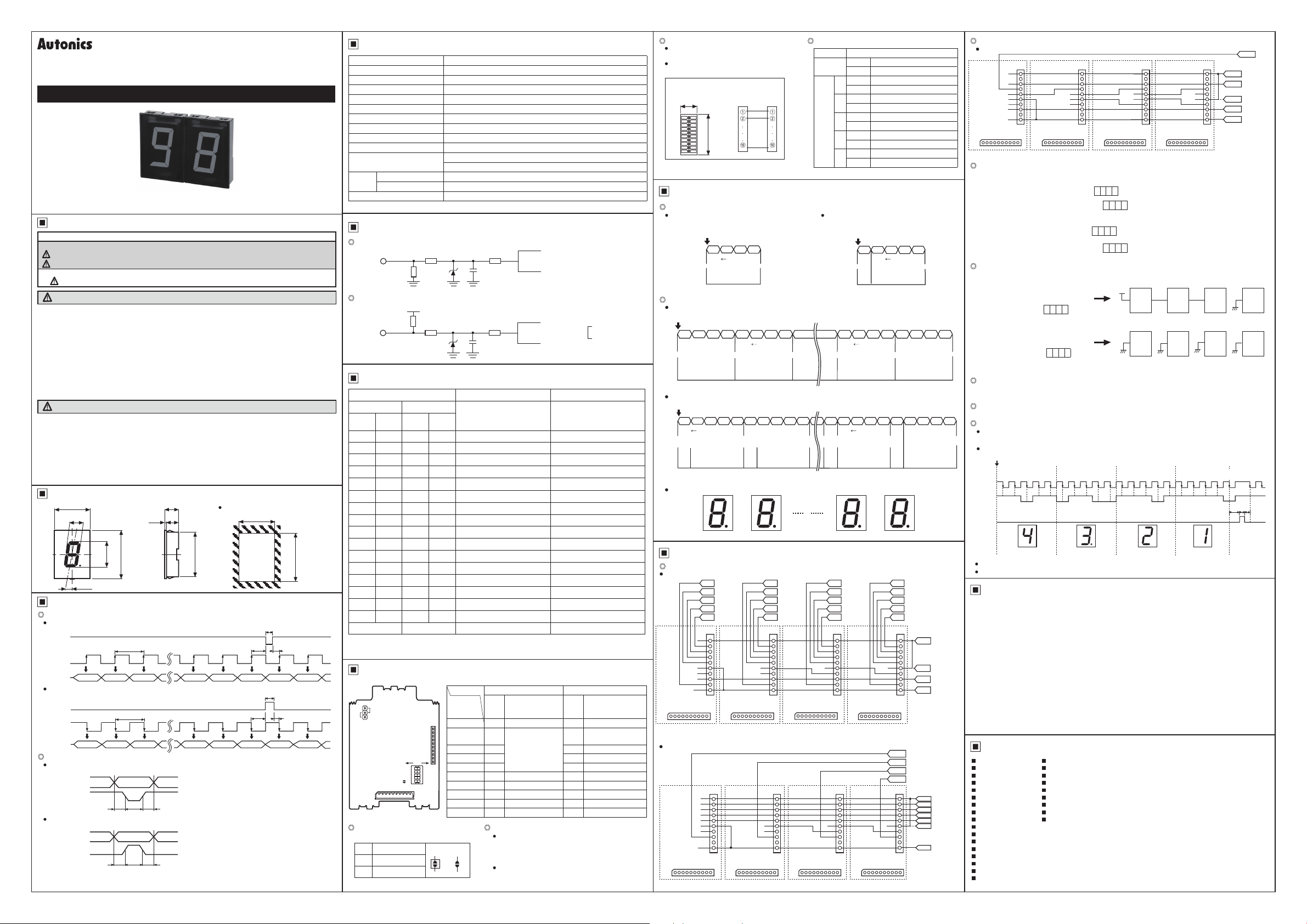
Autonics
DISPLAY UNIT
D1SC-N
I N S T R U C T I O N M A N U A L
Thank you very much for selecting Autonics products.
For your safety, please read the following before using.
Safety Considerations
00
※
Please observe all safety considerations for safe and proper product operation to avoid hazards.
※
Safety considerations are categorized as follows.
Warning Failure to follow these instruc ions may result in serious injury or death.
Caution
※
1. Fail-safe device must be installed when using the unit with machinery that may cause serious injury
or substantial economic loss. (e.g. nuclear power control, medical equipment, ships, vehicles,
railways, aircraft, combustion apparatus, safety equipment, crime/disaster prevention devices, etc.)
Failure to follow this instruction may result in fire, personal injury, or economic loss.
2. Install on a device panel to use.
Failure to follow this instruction may result in fire.
3. Do not connect, repair
Failure to follow this instruction may result in fire.
4. Check 'Unit description and function setting' before wiring.
Failure to follow this instruction may result in fire.
5. Do not disassemble or modify the unit.
Failure to follow this instruction may result in fire.
1. Use the unit within the rated specifications.
Failure to follow this instruction may result in fire or product damage.
2. Use dry cloth to clean the unit, and do not use water or organic solvent.
Failure to follow this instruction may result in fire.
3. Do not use the unit in the place where flammable/explosive/corrosive gas, humidity, direct sunlight,
radiant heat, vibration, impact, or salinity may be present.
Failure to follow this instruction may result in fire or explosion.
4. Keep metal chip, dust, and wire residue from flowing into the unit.
Failure to follow this instruction may result in fire or product damage.
Dimensions
00
Input Timing
00
g
Serial input
Positive logic(SW1:OFF, SW2-
•
Negative logic(SW1:ON, SW2-
•
Parallel input
Positive logic(SW1:OFF, SW2-
Negative logic((SW1:ON, SW2-
※
The above specications are subject to change and some models may be discontinued without notice.
※
Be sure to follow cautions written in the instruction manual and the technical descriptions
(catalog, homepage).
Failure to follow these instructions may result in personal injury or product damage.
The symbols used on the product and instruction manual represent the following
symbol represents caution due to special circumstances in which hazards may occur.
Warning
, or inspect the unit while connected to a power source.
Caution
72
31 9
96
56.9
10°
※
Applicable panel thickness : 2~4mm
LATCH
CLOCK
DATA
1 2 3 N-2 N-1 N 1 2
LATCH
CLOCK
~t
1 2 3 N-2 N-1 N 1 2
DATA
-c::=::x::::=:xi__A.___,,,'--~--
Input data
Data Latch
Input data
Data Latch
0.33ms
C1
C2
0.33ms
C1
C2
Pw
t1 t2 t3
Pw
t1 t2 t3
28
25.7
2 3
:OFF, SW2-④ • ⑤:ON):Clock 3kHz max.
②
C3
:OFF, SW2-④ • ⑤:ON):Clock 3kHz max.
②
C3
:ON)
②
{
:ON)
②
{
Panel cut-out
72×N-3 5(N:Unit Q'th)
90
CN-2 CN-1
CN-2 CN-1
Pw=t1+t2+t3
Pw:0.33ms(Min.)
t1:0.05ms(Min.) t1:Data latch(Latch)
t2:0.23ms(Min.) t2:Data shift
t3:0.05ms(Min.) t3:Data latch(Latch)
Pw=t1+t2+t3
Pw:0.33ms(Min.)
t1:0.05ms(Min.) t1:Data latch(Latch)
t2:0.23ms(Min.) t2:Data shift
t3:0.05ms(Min.) t3:Data latch(Latch)
tw
ta
tb
tw
ta
tb
90.6
ta:0.23ms(Min.)
tb:0.05ms(Min.)
{
tw:0.05ms(Min.)
C1 C2
ta:0.23ms(Min.)
tb:0.05ms(Min.)
{
tw:0.05ms(Min.)
C1 C2
(Unit:mm)
Specications
00
Model D1SC-N
Indication Red(7 Segment)
Power supply 12-24VDC
Allowable operation voltage 90 to 110% rated voltage
Current consumption Max. 70mA
Max. clock speed Max. 3kHz[When duty rate is 1:1(ON:OFF)]
Input logic Selectable positive or negative logic by slide switch
Input impedance 12kΩ
Input level [High] : 4 5-24VDCᜡ, [Low] : 0-1.2VDC
Insulation resistance 100MΩ Min (at 500VDC)
Noise strength
Ambient temperature 0 to 60℃, Storage: -10 to 85℃ (at non-freezing status)
Environ
I
-ment
Ambient humidity 35 ~ 85%RH
J
Weight Approx. 100g
Input Circuit
00
ᜡ
ᜡ
The square wave noise by simulator(pulse width:1㎲)
±300V between power terminals, ±300V between input terminals
Positive logic(SW1:OFF)
Input
10kΩ
12kΩ
20kΩ
IC
Negative logic(SW1:ON)
+5V
12kΩ
Input
Input Data Chart
■
00
10kΩ
20kΩ
※
Input level
IC
HIGH:4.5-24VDC
[
LOW 0-1.2VDC
Indication Negative input Positive input
Decimal
Blank
Blank
Blank
Blank
Blank
OFF
indication
-li-
7 Segment
Hexa
decimal
0 0
1 1
2 2
3 3
4 4
5 5
6 6
7 7
8 8
9 9
A
B
C
D
E
F
: Minus indication
-
CN2
ON
OFF
5
1
SW2JP1
101
(ON) (OFF)
D C B A LATCH D C B A LATCH
Decimal
H H H H H L L L L L
H H H L H L L L H L
H H L L H L L H L L
H H L L H L L H H L
H L H H H L H L L L
H L H L H L H L H L
H L L H H L H H L L
H L L L H L H H H L
L H H H H H L L L L
L H H L H H L L H L
Blank L H L H H H L H L L
Blank L H L L H H L H H L
Blank L L H H H H H L L L
Blank L L H L H H H L H L
Blank L L L H H H H H L L
Blank L L L L H H H H H L
Input
Terminal
I~
No.(CN1
or CN2)
1 VCC Power(12-24VDC) VCC Power(12-24VDC)
2 A
3 B
4 C
5 D
6 BI Zero blank input BI Zero blank input
7 BO Zero blank input BO Zero blank input
8 LE Latch input LE Latch input
9 DP Decimal point input DP Decimal point input
10 GND GND GND GND
Parallel input Serial input
Code Function Code Function
0
2
1
2
Data input
2
}
2
3
2
Connector specication(CN1)
Connector maker Korea Morex.
• Housing : 5264-10
• Header : 5264-10A(Straight)
.L
'I'
• Terminal : 5263(PBT)
Using cable specification
• AWG#22 ~ 28(Cable diameter : ø1 9mm Max.)
• Sheding length of wire cover : 2.4 ~ 2.9mm
NC
CK Clock input
DI Data input
DO Data input
Don't connect
anything
Minus
Hexa
decimal
Blank Blank
Blank Blank
**
- -
- -
- -
- -
- -
Blank Blank
- -
- -
-
-
Blank Blank
-
-
-
HOLD HOLD X X X X L X X X X H
※
"X" : Don't care,**
※
In case of indicating minus(-), JP1 must be OFF
Unit Description and Fucntion setting
00
ON
SW1
CN1
(Rear terminal layout)
JP1 : Selection of minus(-)
JPI Indication
ON 7 Segment
r------t----ii
OFF Minus
※
"JP1-ON" Factory specication.
CN2 : Connector for multi-stage
This connector must be used with
connection PCB
CN1 and CN2 must be connected as below
drawing.
< Multi-mounting
connector>
8mm
CN1 CN2
27mm
iJ
Data Input Method for Serial
00
Single input method
4Bit Data input(SW2-
SW2-③:OFF, SW2-④:ON, SW2-⑤:ON)
START
fX?C9
I I
Multi-stage connection input method
4Bit Data input(SW2-
•
START
1 2 3 4 5 6 7 8
MSB(N-1)
trnro
10
5Bit Data input(SW2-
•
START
2
1
SH FT SHIFT
MSB(N-1)
DP(N-1)
~
Decimal
Point(N-1)
Arragement
•
[HJ
Multi-stage Connection Method
00
g
Parallel input(These diagrams are to wire at rear layout of the unit)
Static connection(Zero Blanking method) : 4digit
•
1 1
CN1 CN1 CN1 CN1
.
===mnl
l
____
raaaaaaaoaa1
※
Dynamic connection(Zero blanking method) : 4digit
•
CN1 CN1 CN1 CN1
DP0
D 0 D 1 D 2 D 3
C 0 C 1 C 2 C 3
B 0 B 1 B 2 B 3
A 0
CN2
VCC
A
B
C
D
BI
BI
LE
DP
GND
10 10
0
10
CN1 terminal can use instead of CN2, because CN2 corresponds to CN1.
CN2
VCC
BI
BI
LE
GND
1 1 1 1
(0000000000
0
10
:OFF,
②
1122334
SHIFT SH FT
MSB
1 DIGIT
N-1
3
4 5
10
LSB
:OFF, SW2-③:OFF, SW2-④:ON, SW2-⑤:ON)
②
SH FT SH FT
MSB(N-2)
LSB(N-1)
N-2
10
:OFF, SW2-③:ON, SW2-④:ON, SW2-⑤:ON)
②
6
7 8 9 10
MSB(N-2)
LSB(N-1)
DP(N-2)
N-1
Decimal
Point(N-2)
[HJ
N-1
10
1
10
(
__
; ~ ------~-~--------------"""-
1 1 1 1
A
B
C
D
10 10 10 10
10 10 10 10
I
N-2
10
DP1 DP2 DP3
A 1 A 2 A 3
1 1 1
CN2
VCC
A
B
C
D
BI
BI
LE
DP
GND
10 10 10
ooooooool
1
10
CN2
VCC
A
B
C
D
BI
BI
LE
GND
(0000000000
I
1
10
SW1, 2 : Mode selection(DIP SW)
Switch Function
ON* Negative logic
SW1
OFF Positive logic
ON* Progressing by 10(Decimal)
1
OFF Progressing by 16(Hexa decimal)
ON* Parallel
2
OFF Serial
ON Serial DOT (Have)
3
SW2
OFF* Serial DOT (Non)
ON Serial Data OUT (Have)
4
OFF* Serial Data OUT (Non)
ON Blank OUT (Have)
5
OFF* Blank OUT (Non)
"*" : Factory specication.
5Bit Data input((SW2-
SW2-③:ON, SW2-④:ON, SW2-⑤:ON)
START
4N-7 4N-6 4N-5 4N-4 4N-3 4N-2 4N-1 4N
LSB(N-2)
LSB(N-2)
N-2
10
∬
1
....
(ooooooooool
10
(00000000001
MSB(1)
5N-9 5N-8 5N-7 5N-6 5N-5 5N-4 5N-3 5N-2 5N-1 5N
MSB(1)
DP(1)
Decimal
Point(1)
[HJ
1
10
CN2
VCC
A
B
C
D
BI
BI
LE
DP
GND
10
__
i
~----~~~-~-~~~~-~-~~~--
2
CN2
VCC
A
B
C
D
BI
BI
LE
GND
2
10
1
②
MSB
DP
1 DIGIT
LSB(1)
1
10
LSB(1)
1
Decimal
10
Point(0)
[HJ
CN2
VCC
A
B
C
D
BI
BI
LE
DP
GND
3
10
LATCH0
LATCH1
LATCH2
LATCH3
CN2
VCC
A
B
C
D
BI
BI
LE
GND
3
10
:OFF,
MSB(0)
DP(0)
10
10
4 5
MSB(0)
0
}
10
VCC
BO
LATCH
GND
VCC
A
B
C
D
BO
GND
LSB
0
10
Data
input
When over
2digit, BI will
be common
to VCC in
the last digit.
When over
4digit, BI will
be common
to VCC in
the last digit.
Serial input(These diagrams are to wire at rear layout of the unit)
Serial connection(Zero blanking method) : 4digit
•
CN2
VCC
GND
1 1 1 1
roooooooooo
CN1 CN1 CN1 CN1
: ..................... . : ..................... .
0
10
Zero blanking method?
t is to remove "" indication which is no meaning.
EX)When indication value is "10" in 4digit LED
Zero blanking function is applied :
①
Zero blanking function is not applied :
②
EX)When indication value is "101" in 4digit LED
Zero blanking function is applied :
①
Zero blanking function is not applied :
②
How to use zero blanking of D1SC-N
BI input terminal of highest-rank digit must be connected with VCC, BI input terminals of lowest-rank digit must
be connected with GND, but BI input terminals of middle-rank digit connect with BO terminal of one upper-digit.
Zero blanking function is applied
①
-In case of indicating "10"
Zero blanking function is applied
②
In case of indicating "10"
LSB(0)
DP indication for 4Bit serial data input
-Positive logic input : DP input terminal which is going to indicate DP connects with VCC.
-Negative logic input : DP input terminal which is going to indicate DP connects with GND.
DP indication for 5Bit serial data input
-Please input DP data with serial data. (DP data is highest-rank Bit among 5 Bit)
Serial connection example
Input mode:Negative logic of serial decimal with DOT
-SW1:ON, SW2(①:ON, ②:OFF, ③:ON, ④:ON, ⑤:ON), JP1:ON
Display value:43.21 Data input
LSB(0)
0
START ← SHIFT
Data input
1
chart
DP
CLOCK
DATA
LATCH
Data is recorded when clock changes from high to low.
In negative logic, data is read while Latch signal is held at High, but data is held when it change to low.
Cautions during Use
00
1. Follow instructions in 'Cautions during Use'.
Otherwise, t may cause unexpected accidents
2. 12-24VDC power supply should be insulated and limited voltage/current or Class 2, SELV power
supply device.
3. Install a power switch or circuit breaker in the easily accessible place for supplying or disconnecting
the power.
4. Keep away from high voltage lines or power lines to prevent inductive noise.
In case installing power line and input signal line closely
shielded wire at input signal line.
Do not use near the equipment which generates strong magnetic force or high frequency noise.
5. This unit may be used in the following environments.
①
Indoors (in the environment condition rated in 'Specifications')
Altitude max. 2,000m
②
Pollution degree 2
③
Installation category I
④
Main Product
00
Photoelectric Sensors Temperature Controllers
■ ■
Fiber Optic Sensors Temperature/Humidity Transducers
■ ■
Door Sensors SSRs/Power Controllers
■ ■
Door Side Sensors Counters
■ ■
Area Sensors Timers
■ ■
Proximity Sensors Panel Meters
■ ■
Pressure Sensors Tachometers/Pulse (Rate) Meters
■ ■
Rotary Encoders Display Units
■ ■
Connector/Sockets Sensor Controllers
■ ■
Switching Mode Power Supplies
■
Control Switches/Lamps/Buzzers
■
I/O Terminal Blocks & Cables
■
Stepper Motors/Drivers/Motion Controllers
■
Graphic/Logic Panels
■
Field Network Devices
■
Laser Marking System (Fiber, Co₂, Nd:YAG)
■
Laser Welding/Cutting System
■
1 1 1 1
CK
DI
DO
BI
BO
LE
10 10 10 10
10 10 10 10
I
2
3
D
C
3
10
roooooooooo
1
10
1 0
ITIIJ
4digit 3digit 2digit 1digit
1 0
ITIIJ
4dig t 3digt 2dig t 1dig t
6
4
5
DP
B
A
CN2
VCC
GND
CK
DI
DO
BI
BO
LE
I
7
D
10
(0000000000
: .................... .
10
1 0
ITIIJ
4digit 3digit 2digit 1digit
1 0
ITIIJ
4digit 3digit 2digit 1digit
1 0 1
ITIIJ
4digit 3digit 2digit 1digit
1 0 1
ITIIJ
4digit 3digit 2digit 1digit
VCC
-.
fr-D-OI[J
-.
I[]
GND GND
8
9
10
C
DP
B
A
2
.
CN2
VCC
CK
DI
DO
BI
BO
LE
GND
I
(0000000000
--------------·······
2
("0" of 4 and 3digit is removed)
( 4digit is removed, but "0"
of 2digit is indicated)
BI
BO
4digit
(The device viewed from front layout the unit)
BI
BO
4digit
(The device viewed from front layout the unit)
11
12
13
D
C
[2]
10
, use line filter or varistor at power line and
GND
I[]
14
15
B
1
BI
BI
A
3digit
3digit
10
BO
BO
16
DP
CN2
VCC
CK
DI
DO
BI
BO
LE
GND
I
3
BI
BO
2digit
BI
BO
I[]
GND GND
2digit
ta : 0.23ms(Min.)
tb : 0.05ms(Min.)
{
tw : 0.05ms(Min.)
17
18
19
D
C
B
[]
0
10
D1
(Data input)
VCC
CK
When over
4digit, BI will
be common
BO
to VCC in
LATCH
the last digit.
GND
BI
BO
GND
1digit
BI
BO
I[]
1digit
1
20
DP
A
ta twtb
DR W17115 8A A
2
D
 Loading...